JP7032052B2 - Silicone resin film and its manufacturing method, and semiconductor device manufacturing method - Google Patents
Silicone resin film and its manufacturing method, and semiconductor device manufacturing method Download PDFInfo
- Publication number
- JP7032052B2 JP7032052B2 JP2017079140A JP2017079140A JP7032052B2 JP 7032052 B2 JP7032052 B2 JP 7032052B2 JP 2017079140 A JP2017079140 A JP 2017079140A JP 2017079140 A JP2017079140 A JP 2017079140A JP 7032052 B2 JP7032052 B2 JP 7032052B2
- Authority
- JP
- Japan
- Prior art keywords
- film
- organopolysiloxane composition
- group
- semiconductor device
- catalyst
- Prior art date
- Legal status (The legal status is an assumption and is not a legal conclusion. Google has not performed a legal analysis and makes no representation as to the accuracy of the status listed.)
- Active
Links
- 0 CC[C@@]1*CCC1 Chemical compound CC[C@@]1*CCC1 0.000 description 2
Images


Landscapes
- Structures Or Materials For Encapsulating Or Coating Semiconductor Devices Or Solid State Devices (AREA)
- Led Device Packages (AREA)
- Manufacture Of Macromolecular Shaped Articles (AREA)
- Compositions Of Macromolecular Compounds (AREA)
- Silicon Polymers (AREA)
Description
本発明は、シリコーン樹脂フィルム及びその製造方法に関する。より詳細には、触媒を含まない硬化型オルガノポリシロキサン組成物を硬化してシリコーン樹脂フィルムを製造する方法に関する。また、本発明は、金属触媒を実質的に含まないシリコーン樹脂フィルムに関する。
さらに本発明は、前記触媒を含まない硬化型オルガノポリシロキサンの膜状硬化物を備える半導体デバイスの製造方法に関する。
The present invention relates to a silicone resin film and a method for producing the same. More specifically, the present invention relates to a method for producing a silicone resin film by curing a curable organopolysiloxane composition containing no catalyst. The present invention also relates to a silicone resin film that does not substantially contain a metal catalyst.
Further, the present invention relates to a method for manufacturing a semiconductor device including a film-like cured product of a curable organopolysiloxane that does not contain the catalyst.
LEDは現代社会の様々な分野で利用されており、需要はますます広がりを見せている。特に白色LEDは携帯電話や小型照明だけでなく、一般照明や大型ディスプレイなど非常に幅広く使用されるようになった。この白色LEDを製造する方法として、一般的には青色LEDに450nmの光を励起するYAG(イットリウムアルミニウムガーネット)と呼ばれる蛍光体を用いる方式と、3in1とよばれる赤・緑・青色LEDを同時に発光させる方式が知られている。上記の青色LEDと蛍光体を用いる方式は3in1方式に比べ、LED数やワイヤー数が少ないために安価で製造できることから、様々なLEDに対してこの方式が用いられている。 LEDs are used in various fields of modern society, and the demand is expanding more and more. In particular, white LEDs have come to be used very widely not only in mobile phones and small lighting, but also in general lighting and large displays. As a method for manufacturing this white LED, a method using a phosphor called YAG (yttrium aluminum garnet) that excites light of 450 nm into a blue LED and a red / green / blue LED called 3in1 are simultaneously emitted. The method of making it is known. Compared to the 3in1 method, the above method using a blue LED and a phosphor can be manufactured at low cost because the number of LEDs and the number of wires is small, so this method is used for various LEDs.
しかし、YAGなどの蛍光体が混合された液状シリコーン封止材でLEDデバイスを封止して熱硬化する際に、加熱により液状封止材が低粘度化するため、封止材内の蛍光体が沈降してしまい、LEDの色ばらつきが大きくなってしまうことが問題となっていた。その対策として、蛍光体層と透明層を設けた半固体または固体状のフィルムをチップに貼りあわせることで色バラツキを改善することが提案されている(特許文献1)。 However, when the LED device is sealed with a liquid silicone encapsulant mixed with a phosphor such as YAG and heat-cured, the liquid encapsulant becomes less viscous due to heating, so that the phosphor in the encapsulant Has settled down, and there has been a problem that the color variation of the LED becomes large. As a countermeasure, it has been proposed to improve color variation by adhering a semi-solid or solid film provided with a phosphor layer and a transparent layer to a chip (Patent Document 1).
電子材料関連材料は使用基材の最小化、微細パターン化、高耐熱、高耐衝撃などが要求されており、現在は様々な樹脂が使用されている。基材の最小化に伴い、封止材やコート材に含まれる微量の金属触媒が、熱や光などによる変色、信頼性低下の原因のひとつになっている。また、フォトカプラ、CCD、CMOSといった光学センサなどは、センサの微細化、高性能化に伴い、耐熱・耐光性・耐衝撃性などの信頼性も重視され、従来のセンサなどをガラスで封止しただけではクラックが発生するなどの問題も起こっている。 Electronic material-related materials are required to minimize the base material used, have fine patterns, have high heat resistance, and have high impact resistance, and various resins are currently used. With the minimization of the base material, a small amount of metal catalyst contained in the encapsulant and the coating material is one of the causes of discoloration and deterioration of reliability due to heat and light. In addition, for optical sensors such as photocouplers, CCDs, and CMOS, reliability such as heat resistance, light resistance, and impact resistance is also emphasized as the sensors become finer and higher in performance, and conventional sensors are sealed with glass. There are also problems such as cracks occurring just by doing so.
特許文献4には層状ホットメルトシリコーン組成物を用いてセンサなどの材料を圧縮成形などで成形し製造する方法が記載されている。しかし実際は付加反応触媒が使用されており、耐熱・耐光特性のさらなる向上を達成することは困難であった。特許文献5には、ポリシラザンを含有し、真空紫外線照射処理をすることによりガスバリア層を設けることが記載されているが、ガスバリア層はそれほど厚くすることができず、ポリマーの柔軟性に問題があった。特許文献6には熱膨張性微小球を含有した粘着層にチップを搭載し、保護物質で被覆し、粘着層を剥離しダイシングするというチップサイズパッケージの製造方法が記載されている。しかし粘着層が必要で、熱硬化性樹脂には必ず触媒が入っており、耐熱性向上達成は困難であった。
特許文献1に記載の熱硬化性シリコーン樹脂組成物のように、従来の熱硬化性シリコーン樹脂組成物は金属触媒を含有する。そのため、得られる硬化物中には金属触媒が残ってしまう。該硬化物は、耐熱変色性や信頼性が十分ではなく、これらの問題は硬化物中に残る触媒の量に依存していることがわかった。そのため、硬化物の原料である熱硬化性シリコーン樹脂組成物中に含まれる金属触媒量の低減が課題となっている。また、金属触媒含有のシリコーン樹脂組成物は、一液タイプの場合には徐々に反応性が変化して経時変化を生じるために保存安定性が悪い。また、二液タイプの場合は、混合してフィルム状に成形する際にボイドが発生しやすいという問題も有する。
さらに、低ガス透過性を有するポリシラザンやアクリレートを用いた化合物では樹脂の柔軟性や耐熱変色性に問題があった。
Like the thermosetting silicone resin composition described in
Further, the compound using polysilazane or acrylate having low gas permeability has a problem in the flexibility of the resin and the heat-resistant discoloration property.
本発明は上記事情に鑑み、金属触媒を含まず、未硬化状態での保存安定性が高い硬化型のシリコーン樹脂組成物を硬化してフィルムを製造する方法を提供すること、及び耐熱性及び信頼性を高めたシリコーン樹脂フィルムを提供することを目的とする。さらに本発明は前記シリコーン樹脂組成物を基板に貼りあわせて硬化する工程を含む、耐熱性及び信頼性を高めたシリコーン含有デバイスを提供することを目的とする。 In view of the above circumstances, the present invention provides a method for producing a film by curing a curable silicone resin composition which does not contain a metal catalyst and has high storage stability in an uncured state, and has heat resistance and reliability. It is an object of the present invention to provide a silicone resin film having enhanced properties. Further, an object of the present invention is to provide a silicone-containing device having improved heat resistance and reliability, which comprises a step of adhering the silicone resin composition to a substrate and curing it.
特表2014-519964号公報(特許文献2)及び特表2015-511164号公報(特許文献3)には、無機/有機ポリマーハイブリッド材料の表面及び内部に金属触媒が固定された触媒活性を有する触媒材料、特には触媒膜が記載されている。該触媒膜は溶媒及び気体に対して浸透性があり、溶液中または液体・気体二相系中での化学反応を触媒するために使用可能であると記載されている。特許文献2及び3には、上記触媒膜を固体中での反応に使用すること、あるいは反応が進むにつれて反応系が固体化する反応へ使用することは記載されていない。
In Japanese Patent Application Laid-Open No. 2014-516964 (Patent Document 2) and Japanese Patent Application Laid-Open No. 2015-511164 (Patent Document 3), a catalyst having a catalytic activity in which a metal catalyst is immobilized on the surface and inside of an inorganic / organic polymer hybrid material. Materials, especially catalyst films, are described. It is stated that the catalyst membrane is permeable to solvents and gases and can be used to catalyze chemical reactions in solution or in liquid / gas two-phase systems.
本発明者らは、熱硬化性オルガノポリシロキサン組成物を硬化する触媒として、上記のような金属触媒が固定された触媒活性を有する膜(以下、触媒膜という)を使用することを鋭意検討したところ、触媒を含まない硬化型オルガノポリシロキサン組成物を膜状に成形し、触媒膜に貼り合せて加熱硬化すると、オルガノポリシロキサン組成物が硬化してフィルム状成形物を与えることを見出した。さらに、触媒膜をフィルム状成形物から剥離することにより、含まれる金属触媒量が極めて少ないシリコーン樹脂フィルムを提供できることを見出し、本発明を成すに至った。
さらに本発明者らは、触媒を含まない硬化性オルガノポリシロキサン組成物を膜状に成形し、触媒膜に貼り合せた後、硬化性オルガノポリシロキサン組成物面を半導体デバイスに貼り合せて加熱硬化した後、触媒膜をフィルム状成形物から剥離し、ダイシングすることにより、含まれる金属触媒量が極めて少ない半導体デバイスを提供できることを見出し、本発明を成すに至った。
The present inventors have diligently studied the use of a film having catalytic activity (hereinafter referred to as a catalyst film) in which a metal catalyst as described above is fixed, as a catalyst for curing a thermosetting organopolysiloxane composition. However, it has been found that when a curable organopolysiloxane composition containing no catalyst is formed into a film, bonded to a catalyst film and cured by heating, the organopolysiloxane composition is cured to give a film-like molded product. Furthermore, they have found that a silicone resin film containing an extremely small amount of metal catalyst can be provided by peeling the catalyst film from the film-shaped molded product, and have achieved the present invention.
Furthermore, the present inventors mold a curable organopolysiloxane composition containing no catalyst into a film shape, attach it to a catalyst film, and then attach the surface of the curable organopolysiloxane composition to a semiconductor device and heat-cure it. Then, by peeling the catalyst film from the film-shaped molded product and dicing it, it was found that a semiconductor device containing an extremely small amount of metal catalyst can be provided, and the present invention has been completed.
すなわち本発明は、(B)1分子中にケイ素原子に結合した水素原子を少なくとも2個有するオルガノハイドロジェンポリシロキサンを含む硬化型オルガノポリシロキサン組成物を硬化してシリコーン樹脂フィルムを製造する方法であって、該オルガノポリシロキサン組成物は金属触媒を含まず、
前記製造方法は下記工程1)~3)を含み、
1)触媒活性を有する膜1枚の上にて、または2枚の間にて、前記オルガノポリシロキサン組成物を膜状に成形する工程、又は、膜状に成形したオルガノポリシロキサン組成物の少なくとも1面と触媒活性を有する膜とを貼り合わせる工程、
2)次いで、前記オルガノポリシロキサン組成物を硬化してシリコーン樹脂フィルムを得る工程、及び
3)得られたシリコーン樹脂フィルムと前記膜とを剥離する工程
前記触媒活性を有する膜が、膜の表面、又は、膜の表面及び内部に触媒を有することを特徴とする、前記製造方法を提供する。
That is, the present invention is (B) a method for producing a silicone resin film by curing a curable organopolysiloxane composition containing an organohydrogenpolysiloxane having at least two hydrogen atoms bonded to silicon atoms in one molecule. The organopolysiloxane composition does not contain a metal catalyst.
The manufacturing method includes the following steps 1) to 3).
1) A step of forming the organopolysiloxane composition into a film on or between two films having catalytic activity, or at least the organopolysiloxane composition formed into a film. The process of bonding one surface and a film having catalytic activity,
2) Next, a step of curing the organopolysiloxane composition to obtain a silicone resin film, and 3) a step of peeling the obtained silicone resin film from the film. Alternatively, the above-mentioned manufacturing method is provided, which comprises having a catalyst on the surface and inside of the film.
また、本発明は
(B)1分子中にケイ素原子に結合した水素原子を少なくとも2個有するオルガノハイドロジェンポリシロキサンを含む硬化性オルガノポリシロキサン組成物の硬化物を備える半導体デバイスの製造方法であって、該オルガノポリシロキサン組成物は金属触媒を含まず、
前記製造方法は下記工程1)~4)を含み、
1)触媒活性を有する膜1枚の上に、前記オルガノポリシロキサン組成物を膜状に成形する工程、又は、膜状に成形したオルガノポリシロキサン組成物の1面と触媒活性を有する膜とを貼り合わせて膜状積層物を得る工程、
2)次いで、前記工程1)で得た膜状積層物の組成物面と、半導体チップが搭載された基板の半導体チップ搭載面とを貼り合せて、半導体チップを前記オルガノポリシロキサン組成物で被覆する工程、
3)次いで、前記オルガノポリシロキサン組成物を硬化する工程、及び
4)次いで、前記硬化物と前記触媒膜とを剥離して、前記硬化物で半導体チップが被覆された半導体デバイスを得る工程、
前記触媒活性を有する膜が、膜の表面、又は、膜の表面及び内部に触媒を有することを特徴とする、前記半導体デバイスの製造方法を提供する。
該製造方法はさらに、上記工程4)の後に、得られた半導体デバイスをダイシングして個片化する工程を含むことが出来る。
Further, the present invention is (B) a method for producing a semiconductor device including a cured product of a curable organopolysiloxane composition containing an organohydrogenpolysiloxane having at least two hydrogen atoms bonded to silicon atoms in one molecule. The organopolysiloxane composition does not contain a metal catalyst.
The manufacturing method includes the following steps 1) to 4).
1) A step of forming the organopolysiloxane composition into a film on one film having catalytic activity, or one surface of the organopolysiloxane composition formed into a film and a film having catalytic activity. The process of laminating to obtain a film-like laminate,
2) Next, the composition surface of the film-like laminate obtained in the step 1) and the semiconductor chip mounting surface of the substrate on which the semiconductor chip is mounted are bonded together, and the semiconductor chip is coated with the organopolysiloxane composition. Process,
3) Next, a step of curing the organopolysiloxane composition, and 4) Next, a step of peeling the cured product from the catalyst membrane to obtain a semiconductor device in which the semiconductor chip is coated with the cured product.
Provided is a method for manufacturing a semiconductor device, wherein the film having catalytic activity has a catalyst on the surface of the film or on the surface and inside of the film.
The manufacturing method can further include a step of dicing the obtained semiconductor device into individual pieces after the above step 4).
また本発明は、硬化型オルガノポリシロキサン組成物がさらに、(A)1分子中にケイ素原子に結合したアルケニル基を少なくとも2個有するオルガノポリシロキサンを、該(A)成分中のアルケニル基の個数に対する上記(B)成分中のSiH基の個数比が0.5~8となる量で含む、前記シリコーン樹脂フィルム及び半導体デバイスの製造方法を提供する。 Further, in the present invention, the cured organopolysiloxane composition further comprises (A) an organopolysiloxane having at least two alkenyl groups bonded to a silicon atom in one molecule, and the number of alkenyl groups in the component (A). Provided is a method for producing the silicone resin film and the semiconductor device, which comprises the ratio of the number of SiH groups in the component (B) to the above in an amount of 0.5 to 8.
さらに本発明は、(B)1分子中にケイ素原子に結合した水素原子を少なくとも2個有するオルガノハイドロジェンポリシロキサンを含み、且つ、金属触媒を含まないオルガノポリシロキサン組成物の硬化物から成るシリコーン樹脂フィルムであって、該硬化物中に含まれてよい金属触媒の量が硬化物全体の質量に対し金属質量換算として0.1ppm未満である、シリコーン樹脂フィルムを提供する。
また本発明は、(B)1分子中にケイ素原子に結合した水素原子を少なくとも2個有するオルガノハイドロジェンポリシロキサンを含み、さらに(A)1分子中にケイ素原子に結合したアルケニル基を少なくとも2個有するオルガノポリシロキサンを、該(A)成分中のアルケニル基の個数に対する上記(B)成分中のSiH基の個数比が0.5~8となる量で含み、且つ、金属触媒を含まないオルガノポリシロキサン組成物の硬化物から成るシリコーン樹脂フィルムであって、該硬化物中に含まれてよい金属触媒の量が硬化物全体の質量に対し金属質量換算として0.1ppm未満である、シリコーン樹脂フィルムを提供する。
Further, the present invention (B) is a silicone comprising a cured product of an organopolysiloxane composition containing an organohydrogenpolysiloxane having at least two hydrogen atoms bonded to silicon atoms in one molecule and containing no metal catalyst. Provided is a silicone resin film, wherein the amount of a metal catalyst that may be contained in the cured product is less than 0.1 ppm in terms of metal mass with respect to the total mass of the cured product.
Further, the present invention includes (B) an organohydrogenpolysiloxane having at least two hydrogen atoms bonded to a silicon atom in one molecule, and (A) at least two alkenyl groups bonded to a silicon atom in one molecule. The organopolysiloxane having each is contained in an amount such that the ratio of the number of SiH groups in the component (B) to the number of alkenyl groups in the component (A) is 0.5 to 8, and does not contain a metal catalyst. A silicone resin film made of a cured product of an organopolysiloxane composition, wherein the amount of metal catalyst that may be contained in the cured product is less than 0.1 ppm in terms of metal mass with respect to the total mass of the cured product. Provide resin film.
本発明の製造方法では、オルガノポリシロキサン組成物中に金属触媒を含まないため、組成物の硬化時、組成物を未硬化状態で保管する時に、経時で物性変化が起こりにくい。そのため組成物の保存安定性が向上する。また、得られるシリコーン樹脂フィルム中に含まれる金属触媒量が極めて少なく、特には金属触媒を実質的に含有しないため、該シリコーン樹脂フィルムを長期間保管しても経時変化が起こりにくく、信頼性の高い樹脂フィルムを提供できる。さらに該樹脂フィルムは高耐熱性を有することができる。さらに前記オルガノポリシロキサン組成物の膜状硬化物を備える半導体デバイスも耐熱性に優れ、信頼性の高い半導体デバイスを提供できる。 In the production method of the present invention, since the organopolysiloxane composition does not contain a metal catalyst, physical properties are unlikely to change over time when the composition is cured or when the composition is stored in an uncured state. Therefore, the storage stability of the composition is improved. Further, since the amount of the metal catalyst contained in the obtained silicone resin film is extremely small, and in particular, the metal catalyst is substantially not contained, the silicone resin film is less likely to change with time even if it is stored for a long period of time, and is reliable. A high resin film can be provided. Further, the resin film can have high heat resistance. Further, the semiconductor device provided with the film-like cured product of the organopolysiloxane composition also has excellent heat resistance and can provide a highly reliable semiconductor device.
以下、本発明について詳細に説明する。 Hereinafter, the present invention will be described in detail.
本発明は、硬化型オルガノポリシロキサン組成物を硬化して樹脂フィルムを製造する方法であり、該オルガノポリシロキサン組成物が金属触媒を含んでいないこと、硬化触媒として、触媒活性を有する膜(以下、触媒膜という)を使用することを特徴とする。該触媒膜は、膜の表面、又は、膜の表面及び内部にヒドロシリル化反応触媒を有するものである。以下、触媒膜について詳細に説明する。 The present invention is a method for producing a resin film by curing a curable organopolysiloxane composition, wherein the organopolysiloxane composition does not contain a metal catalyst, and a film having catalytic activity as a curing catalyst (hereinafter referred to as a film). , Called a catalyst film). The catalyst membrane has a hydrosilylation reaction catalyst on the surface of the membrane or on the surface and inside of the membrane. Hereinafter, the catalyst membrane will be described in detail.
[触媒膜]
本発明の製造方法で使用される触媒膜とは、触媒が膜の表面に固定されている、又は、膜の表面に固定され及び膜の内部に包埋されている、触媒活性を有する膜である。触媒は膜を構成する支持材料により固定されており、例えば、ポリビニルアルコール(PVA)またはその誘導体、ポリイミド、ポリエチレン、再生セルロース等の有機ポリマーをベースにした膜を使用することができる。特に好ましくは、無機酸化物と、水酸基を有する有機ポリマーのハイブリッド化合物を含む膜である。無機酸化物は水酸基を介して有機ポリマーと化学結合することができ、触媒は該ハイブリット化合物に固定される。該触媒膜としては、特には、特表2014-519964号公報(特許文献2)及び特表2015-511164号公報(特許文献3)に記載されるものを使用できる。以下、更に詳細に説明する。
[Catalyst membrane]
The catalyst membrane used in the production method of the present invention is a membrane having catalytic activity in which the catalyst is fixed to the surface of the membrane or fixed to the surface of the membrane and embedded inside the membrane. be. The catalyst is fixed by a supporting material constituting the membrane, and for example, a membrane based on an organic polymer such as polyvinyl alcohol (PVA) or a derivative thereof, polyimide, polyethylene, or regenerated cellulose can be used. Particularly preferred is a membrane containing a hybrid compound of an inorganic oxide and an organic polymer having a hydroxyl group. The inorganic oxide can be chemically bonded to the organic polymer via a hydroxyl group, and the catalyst is immobilized on the hybrid compound. As the catalyst membrane, those described in JP-A-2014-516964 (Patent Document 2) and JP-A-2015-511164 (Patent Document 3) can be used in particular. Hereinafter, it will be described in more detail.
ハイブリッド化合物を構成する無機酸化物は、ケイ酸化合物やジルコン酸化合物であることが好ましい。ケイ酸化合物は、ケイ酸およびその誘導体、またはケイ酸を主成分として含有する任意の化合物を意味する。ジルコン酸化合物は、ジルコン酸およびその誘導体、またはジルコン酸を主成分として含有する任意の化合物を意味する。特に好ましくはジルコン酸化合物である。また、ケイ酸化合物及びジルコン酸化合物は、その特性が損なわれない範囲で、他の元素を含んでいてもよく、及び/または添加物を含んでいてもよい。 The inorganic oxide constituting the hybrid compound is preferably a silicic acid compound or a zirconate acid compound. Silicic acid compound means silicic acid and its derivatives, or any compound containing silicic acid as a main component. The zirconate compound means zirconate and its derivatives, or any compound containing zirconate as a main component. Particularly preferably, it is a zirconate acid compound. Further, the silicic acid compound and the zirconate compound may contain other elements and / or may contain additives as long as their properties are not impaired.
水酸基を有する有機ポリマーは、水溶性ポリマーが好ましく、特に好ましくはポリビニルアルコールである。その他のポリマーとしては、例えばポリエチレンおよびポリプロピレンなどのポリオレフィンポリマー、ポリアクリルポリマー、酸化ポリエチレンおよび酸化ポリプロピレンなどのポリエーテルポリマー、ポリエチレンテレフタレートおよびポリブチレンテレフタレートなどのポリエステルポリマー、ポリテトラフルオロエチレンおよびポリフッ化ビニリデンなどのフッ素ポリマー、メチルセルロースなどの糖鎖化合物、ポリ酢酸ビニルポリマー、ポリスチレンポリマー、ポリカーボネートポリマー、エポキシ樹脂ポリマーが挙げられる。これらは混合して使用してもよい。また、該触媒膜の特性を損ねない範囲で、他の有機および無機添加物をハイブリッド化合物に混合したものであってもよい。 The organic polymer having a hydroxyl group is preferably a water-soluble polymer, and particularly preferably polyvinyl alcohol. Other polymers include, for example, polyolefin polymers such as polyethylene and polypropylene, polyacrylic polymers, polyether polymers such as polyethylene oxide and polypropylene oxide, polyester polymers such as polyethylene terephthalate and polybutylene terephthalate, polytetrafluoroethylene and polyvinylidene fluoride. Fluoropolymers, sugar chain compounds such as methylcellulose, polyvinyl acetate polymers, polystyrene polymers, polycarbonate polymers, epoxy resin polymers and the like. These may be mixed and used. Further, other organic and inorganic additives may be mixed with the hybrid compound as long as the characteristics of the catalyst membrane are not impaired.
触媒は、金属単体または金属化合物である。例えば、白金族金属又は白金族金属化合物であり、白金族金属系触媒である白金系、パラジウム系、及びロジウム系触媒が好適に使用できる。コスト等の見地から白金系やパラジウム系触媒であることがよく、これら金属の金属微粒子触媒、またはこれら金属元素を含む金属化合物触媒を用いることができる。より詳細には、白金族金属化合物としては、例えば、H2PtCl6・mH2O、K2PtCl6、KHPtCl6・mH2O、K2PtCl4、K2PtCl4・mH2O、PtO2・mH2O(mは、正の整数)が挙げられる。これらの他に、前記白金族金属化合物とオレフィン等の炭化水素、アルコールまたはビニル基含有オルガノポリシロキサンとの錯体等を用いることができ、パラジウム系触媒であればPdCl2などが挙げられる。上記触媒は単独でも、2種以上の組み合わせであってもよい。触媒膜中、上記触媒の量は、金属換算で触媒膜全体の重量に対して0.0001~10wt%、好ましくは0.1~10wt%が好ましい。金属粒子触媒は、直径0.5~500nmを有するものがよい。 The catalyst is a simple substance of metal or a metal compound. For example, platinum-based, palladium-based, and rhodium-based catalysts which are platinum group metals or platinum group metal compounds and which are platinum group metal-based catalysts can be preferably used. From the viewpoint of cost and the like, platinum-based or palladium-based catalysts are often used, and metal fine particle catalysts of these metals or metal compound catalysts containing these metal elements can be used. More specifically, examples of the platinum group metal compound include H 2 PtCl 6 · mH 2 O, K 2 PtCl 6 , KH PtCl 6 · mH 2 O, K 2 PtCl 4 , K 2 PtCl 4 · mH 2 O, PtO. 2. mH 2 O (m is a positive integer). In addition to these, a complex of the platinum group metal compound and a hydrocarbon such as an olefin, an alcohol or a vinyl group-containing organopolysiloxane can be used, and examples of the palladium catalyst include PdCl 2 . The catalyst may be used alone or in combination of two or more. In the catalyst membrane, the amount of the catalyst is preferably 0.0001 to 10 wt%, preferably 0.1 to 10 wt%, based on the total weight of the catalyst membrane in terms of metal. The metal particle catalyst preferably has a diameter of 0.5 to 500 nm.
触媒膜の製造方法は、例えば、特表2014-519964号公報(特許文献2)及び特表2015-511164号公報(特許文献3)に記載される方法に従えばよい。また市販品として、例えば、無機酸化物/ポリビニルアルコールハイブリッド化合物にパラジウムを固定した触媒膜(商品名:Pd-iObrane(登録商標)、ニッポン高度紙工業株式会社製)を使用できる。 The method for producing the catalyst membrane may be, for example, according to the methods described in JP-A-2014-516964 (Patent Document 2) and JP-A-2015-511164 (Patent Document 3). Further, as a commercially available product, for example, a catalyst membrane in which palladium is immobilized on an inorganic oxide / polyvinyl alcohol hybrid compound (trade name: Pd-iObrane (registered trademark), manufactured by Nippon Kodoshi Paper Industry Co., Ltd.) can be used.
本発明は、上記触媒膜を使用して、触媒を含まない硬化型オルガノポリシロキサン組成物を硬化する。該オルガノポリシロキサン組成物を膜状に成形して上記触媒膜と接触させ、加熱することにより、触媒膜の表面で硬化反応が促進され、硬化物を与える。反応中、膜状態の触媒を使用することにより触媒金属粒子の凝集を防止し、触媒活性が一定になる。また、触媒膜に触媒が強力に固定されているため、反応中、触媒が組成物中に移行することは抑制される。そのため、硬化後に該触媒膜を剥離することで、硬化物中に含まれる金属触媒量をきわめて低いものとすることができる。すなわち、本発明の製造方法によれば、硬化物中に含まれる金属触媒量が金属質量換算で0.1ppm未満であるシリコーン樹脂フィルムを提供でき、特には、金属触媒を実質的に含まないシリコーン樹脂フィルムを与えることができる。 The present invention uses the catalyst membrane to cure a curable organopolysiloxane composition that does not contain a catalyst. By molding the organopolysiloxane composition into a film shape, contacting it with the catalyst film, and heating it, a curing reaction is promoted on the surface of the catalyst film to give a cured product. During the reaction, the use of a catalyst in a film state prevents the agglutination of the catalytic metal particles and makes the catalytic activity constant. Further, since the catalyst is strongly fixed to the catalyst membrane, the transfer of the catalyst into the composition during the reaction is suppressed. Therefore, by peeling off the catalyst film after curing, the amount of metal catalyst contained in the cured product can be made extremely low. That is, according to the production method of the present invention, it is possible to provide a silicone resin film in which the amount of metal catalyst contained in the cured product is less than 0.1 ppm in terms of metal mass, and in particular, silicone containing substantially no metal catalyst. A resin film can be given.
[オルガノポリシロキサン組成物]
本発明の製造方法により硬化されるオルガノポリシロキサン組成物には二つの態様がある。第一の態様は、下記(B)成分を単独で含み、脱水素縮合により硬化する組成物である。第二の態様は、下記(A)成分と(B)成分を含み、付加反応により硬化する組成物である。尚、本発明のオルガノポリシロキサン組成物は上記の通り金属触媒を含まない。
(A)1分子中にケイ素原子に結合したアルケニル基を少なくとも2個有するオルガノポリシロキサン
(B)1分子中にケイ素原子に結合した水素原子を少なくとも2個有するオルガノハイドロジェンポリシロキサン
以下、各成分について詳細に説明する。
[Organopolysiloxane composition]
The organopolysiloxane composition cured by the production method of the present invention has two aspects. The first aspect is a composition containing the following component (B) alone and cured by dehydrogenation condensation. The second aspect is a composition containing the following components (A) and (B) and cured by an addition reaction. The organopolysiloxane composition of the present invention does not contain a metal catalyst as described above.
(A) Organopolysiloxane having at least two alkenyl groups bonded to silicon atoms in one molecule (B) Organohydrogenpolysiloxane having at least two hydrogen atoms bonded to silicon atoms in one molecule The following components Will be described in detail.
[(A)アルケニル基含有オルガノポリシロキサン]
(A)成分は、1分子中にケイ素原子に結合したアルケニル基を少なくとも2個、好ましくは3個以上有するオルガノポリシロキサンである。(A)成分は、従来公知のアルケニル基含有オルガノポリシロキサンであればよい。
好ましくは、下記平均組成式(1)で表されるオルガノポリシロキサンである。

The component (A) is an organopolysiloxane having at least two, preferably three or more alkenyl groups bonded to a silicon atom in one molecule. The component (A) may be a conventionally known alkenyl group-containing organopolysiloxane.
It is preferably an organopolysiloxane represented by the following average composition formula (1).
上記式(1)中、R1:炭素数6~10の1価芳香族炭化水素基としては、フェニル基、トリル基、キシリル基、ナフチル基等のアリール基やベンジル基、フェニルエチル基、フェニルプロピル基等のアラルキル基などが挙げられる。中でも、フェニル基、ベンジル基などが好ましく、特にフェニル基が好ましい。R2:炭素数1~10の鎖状脂肪族炭化水素基としては、メチル基、エチル基、プロピル基、イソプロピル基、ブチル基、イソブチル基、tert-ブチル基、ペンチル基、ネオペンチル基、ヘキシル基、オクチル基、ノニル基、デシル基等のアルキル基が挙げられる。R2:炭素数3~10の環状脂肪族炭化水素基としてはシクロペンチル基、シクロヘキシル基、シクロオクチル基等のシクロアルキル基が挙げられる。中でも、メチル基、エチル基、シクロペンチル基、及びシクロヘキシル基が好ましく、メチル基、シクロヘキシル基が特に好ましい。また、R2は、これらの炭化水素基の水素原子の一部又は全部をフッ素、臭素、塩素等のハロゲン原子、またはシアノ基等で置換したものを用いてもよく、例えばクロロメチル基、クロロプロピル基、ブロモエチル基、トリフロロプロピル基等のハロゲン置換アルキル基、及びシアノエチル基が挙げられる。R3:炭素数2~8のアルケニル基としては、ビニル基、アリル基、3-ブテニル基、4-ペンテニル基などが挙げられる。中でも、ビニル基、及びアリル基が好ましく、ビニル基が特に好ましい。Xにおける炭素数1~8の一価炭化水素基は、メチル基、エチル基、プロピル基、イソプロピル基、ブチル基等のアルキル基が挙げられる。好ましくは、メチル基又は水素原子である。 In the above formula (1), as the monovalent aromatic hydrocarbon group having R 1 : 6 to 10 carbon atoms, an aryl group such as a phenyl group, a tolyl group, a xylyl group or a naphthyl group, a benzyl group, a phenylethyl group or a phenylpropi. Examples include an aralkyl group such as a le group. Among them, a phenyl group, a benzyl group and the like are preferable, and a phenyl group is particularly preferable. R 2 : As the chain aliphatic hydrocarbon group having 1 to 10 carbon atoms, a methyl group, an ethyl group, a propyl group, an isopropyl group, a butyl group, an isobutyl group, a tert-butyl group, a pentyl group, a neopentyl group and a hexyl group. , Octyl group, nonyl group, decyl group and other alkyl groups. R 2 : Examples of the cyclic aliphatic hydrocarbon group having 3 to 10 carbon atoms include a cycloalkyl group such as a cyclopentyl group, a cyclohexyl group, and a cyclooctyl group. Of these, a methyl group, an ethyl group, a cyclopentyl group, and a cyclohexyl group are preferable, and a methyl group and a cyclohexyl group are particularly preferable. Further, as R 2 , a part or all of the hydrogen atoms of these hydrocarbon groups may be substituted with a halogen atom such as fluorine, bromine or chlorine, a cyano group or the like, and for example, a chloromethyl group or a chloro may be used. Examples thereof include a halogen-substituted alkyl group such as a propyl group, a bromoethyl group and a trifluoropropyl group, and a cyanoethyl group. R 3 : Examples of the alkenyl group having 2 to 8 carbon atoms include a vinyl group, an allyl group, a 3-butenyl group, a 4-pentenyl group and the like. Of these, a vinyl group and an allyl group are preferable, and a vinyl group is particularly preferable. Examples of the monovalent hydrocarbon group having 1 to 8 carbon atoms in X include an alkyl group such as a methyl group, an ethyl group, a propyl group, an isopropyl group and a butyl group. It is preferably a methyl group or a hydrogen atom.
なお、上記アルケニル基含有オルガノポリシロキサンは、少なくとも1個の1価芳香族炭化水素基を有することが好ましく、特には式(1)中のR1、R2及びR3の全個数に対する1価芳香族炭化水素基(R1)の個数の割合が、20~50%であることが好ましく、更には30~50%が好ましい。1価芳香族炭化水素基がこの範囲内にあることで、得られる組成物が25℃で固体または半固体状態となるため好ましい。尚、本発明において半固体とは、15~30℃の温度を室温として、可塑性を持ちながら流動性を持たない性質を有し、温度・応力・ゆがみなどの外部からのストレスによって液体または固体の性質を呈するという状態をいう。 The alkenyl group-containing organopolysiloxane preferably has at least one monovalent aromatic hydrocarbon group, and is particularly monovalent with respect to the total number of R 1 , R 2 and R 3 in the formula (1). The ratio of the number of aromatic hydrocarbon groups (R 1 ) is preferably 20 to 50%, more preferably 30 to 50%. It is preferable that the monovalent aromatic hydrocarbon group is in this range because the obtained composition becomes a solid or semi-solid state at 25 ° C. In the present invention, the semi-solid has the property of having plasticity but not fluidity at a temperature of 15 to 30 ° C., and is a liquid or solid due to external stress such as temperature, stress, and distortion. It is a state of exhibiting properties.
また、上記式(1)において、aは好ましくは0~0.5、より好ましくは0.05~0.5、さらには0.1~0.5の数であり、bは好ましくは0.1~0.7、より好ましくは0.15~0.65の数であり、cは好ましくは0.01~0.5、より好ましくは0.015~0.5、さらには0.02~0.5の数であり、dは好ましくは0.001~0.2、より好ましくは0.001~0.15の数である。ただし、a+b+c+d=1~2である。 Further, in the above formula (1), a is preferably a number of 0 to 0.5, more preferably 0.05 to 0.5, and further 0.1 to 0.5, and b is preferably 0. The number is 1 to 0.7, more preferably 0.15 to 0.65, c is preferably 0.01 to 0.5, more preferably 0.015 to 0.5, and even 0.02 to 0.02. It is a number of 0.5, and d is preferably a number of 0.001 to 0.2, more preferably a number of 0.001 to 0.15. However, a + b + c + d = 1 to 2.
(A)成分は、直鎖、分岐、環状、及び網目状構造のいずれを有していても良く、R2SiO2/2単位(D単位)、R3SiO1/2単位(M単位)、RSiO3/2単位(T単位)、及びSiO4/2単位(Q単位)のいずれから構成されていてもよい。Rは、R1、R2、R3、又はOX基である。得られる組成物が25℃で半固体状または固体状を有するためには、T単位又はQ単位を少なくとも有するのがよい。特には、T単位、M単位、及びD単位から成り、直鎖構造(連続するD単位)を有するシリコーンレジンが好ましい。該オルガノポリシロキサンは少量のQ単位を含んでいてもよい。(A)成分において、R2SiO2/2で示されるシロキサン単位(D単位)のうち30モル%以上99モル%以下、好ましくは50モル%以上99モル%以下が連続しており、その連続したシロキサン単位の数が5~50個、好ましくは5~40個、更に好ましくは8~40個であるのが好ましい。これにより25℃で固体または半固体状態である組成物が適度な温度で溶融するため、該組成物からなる膜状成形物を触媒膜に貼り合わせる際に扱い易くなる。分子中、アルケニル基が結合するケイ素原子の位置は特に制限されない。 The component (A) may have any of a linear, branched, annular, and mesh-like structure, and has R 2 SiO 2/2 units (D units) and R 3 SiO 1/2 units (M units). , RSiO 3/2 unit (T unit), and SiO 4/2 unit (Q unit). R is an R1 , R2 , R3 , or OX group. In order for the resulting composition to have a semi-solid or solid form at 25 ° C., it should have at least T or Q units. In particular, a silicone resin composed of T units, M units, and D units and having a linear structure (continuous D units) is preferable. The organopolysiloxane may contain a small amount of Q units. In the component (A), 30 mol% or more and 99 mol% or less, preferably 50 mol% or more and 99 mol% or less of the siloxane unit (D unit) represented by R 2 SiO 2/2 are continuous, and the continuation thereof. The number of siloxane units formed is preferably 5 to 50, preferably 5 to 40, and more preferably 8 to 40. As a result, the composition which is in a solid or semi-solid state at 25 ° C. is melted at an appropriate temperature, so that it becomes easy to handle when the film-like molded product made of the composition is bonded to the catalyst film. In the molecule, the position of the silicon atom to which the alkenyl group is bonded is not particularly limited.
該オルガノポリシロキサンは、重量平均分子量が2,000~100,000であることが好ましく、特に5,000~80,000であることが好ましい。なお、本発明中で言及する重量平均分子量とは、ゲルパーミエーションクロマトグラフィ(GPC)によるポリスチレンを標準物質とした重量平均分子量である。該重量平均分子量は特には、下記条件により測定される。
[測定条件]
展開溶媒:テトラヒドロフラン(THF)
流量:0.6mL/min
検出器:示差屈折率検出器(RI)
カラム:TSK Guardcolomn SuperH-L
TSKgel SuperH4000(6.0mmI.D.×15cm×1)
TSKgel SuperH3000(6.0mmI.D.×15cm×1)
TSKgel SuperH2000(6.0mmI.D.×15cm×2)
(いずれも東ソー社製)
カラム温度:40℃
試料注入量:20μL(濃度0.5重量%のTHF溶液)
The organopolysiloxane preferably has a weight average molecular weight of 2,000 to 100,000, and particularly preferably 5,000 to 80,000. The weight average molecular weight referred to in the present invention is a weight average molecular weight using polystyrene as a standard substance by gel permeation chromatography (GPC). The weight average molecular weight is particularly measured under the following conditions.
[Measurement condition]
Developing solvent: Tetrahydrofuran (THF)
Flow rate: 0.6 mL / min
Detector: Differential Refractometer Detector (RI)
Column: TSK Guardcolomn SuperH-L
TSKgel SuperH4000 (6.0mm ID x 15cm x 1)
TSKgel SuperH3000 (6.0mm ID x 15cm x 1)
TSKgel SuperH2000 (6.0 mm ID x 15 cm x 2)
(Both manufactured by Tosoh)
Column temperature: 40 ° C
Sample injection volume: 20 μL (THF solution with a concentration of 0.5 wt%)
[(B)オルガノハイドロジェンポリシロキサン]
(B)成分は、1分子中に少なくとも2個以上のケイ素原子に結合した水素原子を有するオルガノハイドロジェンポリシロキサンである。オルガノハイドロジェンポリシロキサンは架橋剤として作用するものであり、該成分中のケイ素原子に結合した水素原子(以下、SiH基)と成分(A)中のアルケニル基とが付加反応することにより硬化する。かかるオルガノハイドロジェンポリシロキサンは、1分子中に少なくとも2個のSiH基を有すればよく、SiH基を3個以上有するものが好適に用いられる。
[(B) Organohydrogenpolysiloxane]
The component (B) is an organohydrogenpolysiloxane having a hydrogen atom bonded to at least two or more silicon atoms in one molecule. Organohydrogenpolysiloxane acts as a cross-linking agent and is cured by an addition reaction between a hydrogen atom (hereinafter, SiH group) bonded to a silicon atom in the component and an alkenyl group in the component (A). .. The organohydrogenpolysiloxane may have at least two SiH groups in one molecule, and those having three or more SiH groups are preferably used.
(B)成分は、好ましくは下記平均組成式(2)で表される。

上記式(2)において、R1は炭素数6~10の1価芳香族炭化水素基であり、上記(A)のために例示したものが挙げられる。例えば、フェニル基、トリル基、キシリル基、ナフチル基が挙げられ、中でもフェニル基が好ましい。上記式(2)において、R2は、炭素数1~10、好ましくは炭素数1~7の、置換又は非置換の、一価炭化水素基であるのがよい。このようなR2としては、メチル基、エチル基、プロピル基、イソプロピル基、ブチル基、イソブチル基、t-ブチル基、ペンチル基、ネオペンチル基、ヘキシル基、オクチル基、ノニル基、デシル基等のアルキル基;クロロメチル基、クロロプロピル基、ブロモエチル基、トリフロロプロピル基等のハロゲン置換アルキル基、シクロペンチル基、シクロヘキシル基等のシクロアルキル基、及びシアノエチル基等が挙げられる。中でもメチル基が好ましい。上記オルガノハイドロジェンポリシロキサンは、少なくとも1個の1価芳香族炭化水素基を有することが好ましく、特には式(2)中の全R1及びR2の全個数に対する1価芳香族炭化水素基(R1)の個数の割合が、20~50%であることが好ましく、更には30~50%が好ましい。1価芳香族炭化水素基がこの範囲内にあることで、得られる組成物が25℃で固体または半固体状態となるため好ましい。 In the above formula (2), R 1 is a monovalent aromatic hydrocarbon group having 6 to 10 carbon atoms, and examples thereof can be mentioned for the above (A). Examples thereof include a phenyl group, a tolyl group, a xylyl group and a naphthyl group, and a phenyl group is preferable. In the above formula (2), R 2 is preferably a substituted or unsubstituted monovalent hydrocarbon group having 1 to 10 carbon atoms, preferably 1 to 7 carbon atoms. Examples of such R 2 include methyl group, ethyl group, propyl group, isopropyl group, butyl group, isobutyl group, t-butyl group, pentyl group, neopentyl group, hexyl group, octyl group, nonyl group, decyl group and the like. Alkyl groups; examples thereof include halogen-substituted alkyl groups such as chloromethyl group, chloropropyl group, bromoethyl group and trifluoropropyl group, cycloalkyl groups such as cyclopentyl group and cyclohexyl group, and cyanoethyl groups. Of these, the methyl group is preferable. The organohydrogenpolysiloxane preferably has at least one monovalent aromatic hydrocarbon group, and in particular, a monovalent aromatic hydrocarbon group with respect to the total number of all R 1 and R 2 in the formula (2). The ratio of the number of (R 1 ) is preferably 20 to 50%, more preferably 30 to 50%. It is preferable that the monovalent aromatic hydrocarbon group is in this range because the obtained composition becomes a solid or semi-solid state at 25 ° C.
上記式(2)において、eは好ましくは0~1.5の数であり、fは好ましくは0<f≦0.85の数であり、gは好ましくは0<g≦0.5の数であり、hは好ましくは0<h≦0.1の数であり、但しe+f+g+h=1~2を満たす数である。分子中ヒドロシリル基の位置は特に制限されず、分子鎖の末端であっても途中であってもよい。 In the above formula (2), e is preferably a number from 0 to 1.5, f is preferably a number of 0 <f≤0.85, and g is preferably a number of 0 <g≤0.5. H is preferably a number of 0 <h ≦ 0.1, but is a number satisfying e + f + g + h = 1 to 2. The position of the hydrosilyl group in the molecule is not particularly limited and may be at the end or in the middle of the molecular chain.
(B)成分は、直鎖、分岐、環状、及び網目状構造のいずれを有していても良く、R2SiO2/2単位(D単位)、R3SiO1/2単位(M単位)、RSiO3/2単位(T単位)、及びSiO4/2単位(Q単位)のいずれから構成されていてもよい。Rは、R1、R2、水素原子、又はOX基である。得られる組成物が25℃で半固体状または固体状を有するためには、T単位又はQ単位を少なくとも有するのがよい。特には、T単位、M単位、及びD単位から成り、直鎖構造(連続するD単位)を有すシリコーンレジンが好ましい。該オルガノポリシロキサンは少量のQ単位を含んでいてもよい。(B)成分において、R2SiO2/2で示されるシロキサン単位(D単位)のうち30モル%以上99モル%以下、好ましくは50モル%以上99モル%以下が連続しており、その連続したシロキサン単位の数が5~50個、好ましくは5~40個、更に好ましくは8~40個であるのが好ましい。 The component (B) may have any of a linear, branched, annular, and mesh-like structure, and has R 2 SiO 2/2 units (D units) and R 3 SiO 1/2 units (M units). , RSiO 3/2 unit (T unit), and SiO 4/2 unit (Q unit). R is R 1 , R 2 , a hydrogen atom, or an OX group. In order for the resulting composition to have a semi-solid or solid form at 25 ° C., it should have at least T or Q units. In particular, a silicone resin composed of T units, M units, and D units and having a linear structure (continuous D units) is preferable. The organopolysiloxane may contain a small amount of Q units. In the component (B), 30 mol% or more and 99 mol% or less, preferably 50 mol% or more and 99 mol% or less of the siloxane unit (D unit) represented by R 2 SiO 2/2 are continuous, and the continuation thereof. The number of siloxane units formed is preferably 5 to 50, preferably 5 to 40, and more preferably 8 to 40.
また、他のオルガノハイドロジェンポリシロキサンとしては、トリス(ジメチルハイドロジェンシロキシ)メチルシラン、トリス(ジメチルハイドロジェンシロキシ)フェニルシラン、1,1,3,3-テトラメチルジシロキサン、1,3,5,7-テトラメチルシクロテトラシロキサン、両末端トリメチルシロキシ基封鎖メチルハイドロジェンポリシロキサン、両末端トリメチルシロキシ基封鎖ジメチルシロキサン・メチルハイドロジェンシロキサン共重合体、両末端ジメチルハイドロジェンシロキシ基封鎖ジメチルシロキサン・メチルハイドロジェンシロキサン共重合体、両末端トリメチルシロキシ基封鎖メチルハイドロジェンシロキサン・ジフェニルシロキサン共重合体、両末端トリメチルシロキシ基封鎖メチルハイドロジェンシロキサン・ジフェニルシロキサン・ジメチルシロキサン共重合体、(CH3)2HSiO1/2単位とSiO4/2単位とから成る共重合体、(CH3)2HSiO1/2単位とSiO4/2単位と(C6H5)SiO3/2単位とから成る共重合体等が挙げられる。 Examples of other organohydrogenpolysiloxanes include tris (dimethylhydrogensiloxy) methylsilane, tris (dimethylhydrogensiloxy) phenylsilane, 1,1,3,3-tetramethyldisiloxane, 1,3,5. 7-Tetramethylcyclotetrasiloxane, both-ended trimethylsiloxy group-blocked methylhydrogenpolysiloxane, both-ended trimethylsiloxy group-blocked dimethylsiloxane / methylhydrogensiloxane copolymer, both-ended dimethylhydrogensiloxy group-blocked dimethylsiloxane / methylhydro Gensiloxane copolymer, double-ended trimethylsiloxy group-blocked methylhydrogensiloxane / diphenylsiloxane copolymer, double-ended trimethylsiloxy group-blocked methylhydrogensiloxane / diphenylsiloxane / dimethylsiloxane copolymer, (CH 3 ) 2 HSiO 1 A copolymer consisting of 2 units and 4/2 units of SiO, a polymer consisting of 1/2 unit of (CH 3 ) 2 HSiO, 4/2 units of SiO and 3/2 units of (C 6 H 5 ) SiO And so on.
該オルガノハイドロジェンポリシロキサンは、重量平均分子量が1,000~200,000であることが好ましく、特に2,000~100,000であることが好ましい。該重量平均分子量は、ゲルパーミエーションクロマトグラフィ(GPC)によるポリスチレンを標準物質とした重量平均分子量である。測定条件は上記した通りである。 The organohydrogenpolysiloxane preferably has a weight average molecular weight of 1,000 to 200,000, and particularly preferably 2,000 to 100,000. The weight average molecular weight is a weight average molecular weight using polystyrene as a standard material by gel permeation chromatography (GPC). The measurement conditions are as described above.
上記(B)成分は単独で、上記触媒膜存在下で、脱水素縮合反応して硬化することができる。該(B)成分を(A)成分と共に使用する場合、すなわち、オルガノポリシロキサン組成物が付加反応硬化型である場合、該組成物中の(B)成分の量は、上記(A)成分中のアルケニル基の個数に対する、(B)成分中のSiH基の個数比が、通常0.5~8となるような量、好ましくは0.7~5となるような量である。 The component (B) can be cured by a dehydrogenation condensation reaction alone in the presence of the catalyst membrane. When the component (B) is used together with the component (A), that is, when the organopolysiloxane composition is an addition reaction curing type, the amount of the component (B) in the composition is in the above component (A). The ratio of the number of SiH groups in the component (B) to the number of alkenyl groups in (B) is usually 0.5 to 8, preferably 0.7 to 5.
[(C)接着助剤]
本発明のオルガノポリシロキサン組成物は、接着性を付与するため、上記した(A)及び(B)成分以外に接着助剤を含有してよい。接着助剤としては、例えば、一分子中にケイ素原子に結合した水素原子、アルケニル基から選ばれる置換基の1種以上と、ヒドロキシシリル基、アルコキシ基、エポキシ基又は窒素原子を含有する置換基の1種以上を有するオルガノシロキサンオリゴマーが挙げられる。該オルガノシロキサンオリゴマーは、ケイ素原子数4~50個であることが好ましく、より好ましくは4~20個である。なお、上記(A)、(B)成分とは、ヒドロキシシリル基、アルコキシ基、エポキシ基あるいは窒素原子を含有する置換基を含む点で相違するものである。
[(C) Adhesive aid]
The organopolysiloxane composition of the present invention may contain an adhesive aid in addition to the above-mentioned components (A) and (B) in order to impart adhesiveness. As the adhesion aid, for example, one or more substituents selected from a hydrogen atom bonded to a silicon atom and an alkenyl group in one molecule, and a substituent containing a hydroxysilyl group, an alkoxy group, an epoxy group or a nitrogen atom. Examples thereof include an organosiloxane oligomer having one or more of the above. The organosiloxane oligomer preferably has 4 to 50 silicon atoms, more preferably 4 to 20 silicon atoms. The components (A) and (B) are different from each other in that they contain a substituent containing a hydroxysilyl group, an alkoxy group, an epoxy group or a nitrogen atom.
接着助剤としては、例えば、ビニルトリメトキシシラン、ビニルトリエトキシシラン、2-(3,4-エポキシシクロヘキシル)エチルトリメトキシシラン、3-グリシドキシプロピルトリメトキシシラン、3-グリシドキシプロピルメチルジエトキシシラン、3-グリシドキシプロピルトリエトキシシラン、3-メタクリロキシプロピルメチルジメトキシシラン、3-メタクリロキシプロピルトリメトキシシラン、3-メタクリロキシプロピルメチルジエトキシシラン、3-メタクリロキシプロピルトリエトキシシラン、N-2-(アミノエチル)-3-アミノプロピルメチルジメトキシシラン、N-2-(アミノエチル)-3-アミノプロピルトリメトキシシラン、N-2-(アミノエチル)-3-アミノプロピルトリエトキシシラン、3-アミノプロピルトリメトキシシラン、3-アミノプロピルトリエトキシシラン、N-フェニル-3-アミノプロピルトリメトキシラン、3-メルカプトプロピルトリメトキシシラン等のシランカップリング剤や、トリメトキシシラン、テトラメトキシシラン及びそのオリゴマーが挙げられる。 Examples of the adhesion aid include vinyltrimethoxysilane, vinyltriethoxysilane, 2- (3,4-epoxycyclohexyl) ethyltrimethoxysilane, 3-glycidoxypropyltrimethoxysilane, and 3-glycidoxypropylmethyl. Diethoxysilane, 3-glycidoxypropyltriethoxysilane, 3-methacryloxypropylmethyldimethoxysilane, 3-methacryloxypropyltrimethoxysilane, 3-methacryloxypropylmethyldiethoxysilane, 3-methacryloxypropyltriethoxysilane , N-2- (aminoethyl) -3-aminopropylmethyldimethoxysilane, N-2- (aminoethyl) -3-aminopropyltrimethoxysilane, N-2- (aminoethyl) -3-aminopropyltriethoxy Silane coupling agents such as silane, 3-aminopropyltrimethoxysilane, 3-aminopropyltriethoxysilane, N-phenyl-3-aminopropyltrimethoxylane, 3-mercaptopropyltrimethoxysilane, trimethoxysilane, tetra. Examples thereof include methoxysilane and its oligomers.
また、他の接着助剤として、下記一般式(3)で示されるオルガノオキシシリル変性イソシアヌレート化合物、及びその加水分解縮合物(オルガノシロキサン変性イソシアヌレート化合物)を使用することができる。
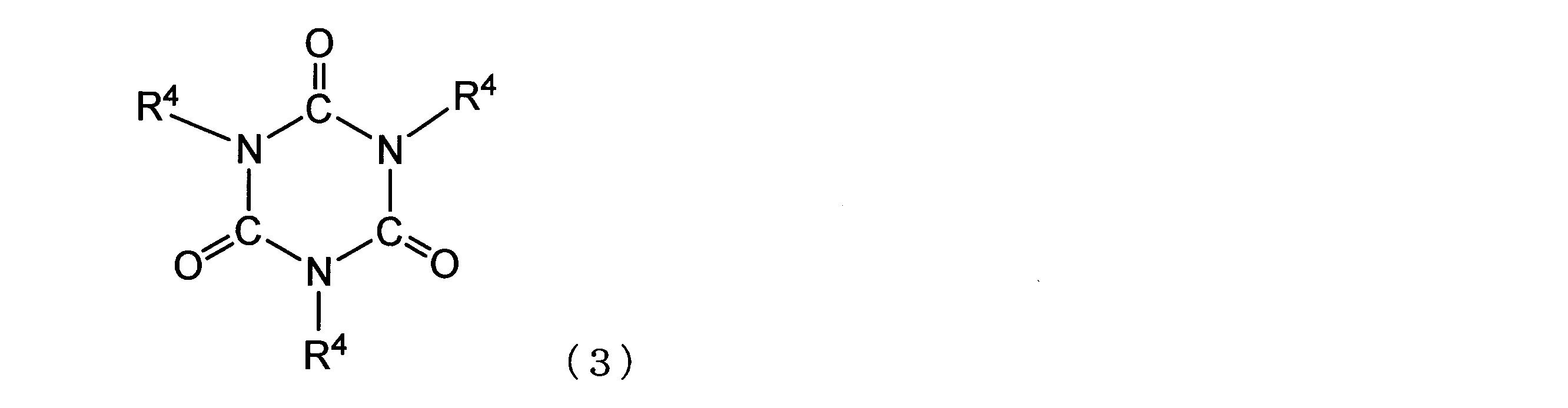
上記式(3)中、R4は互いに独立に、下記一般式(4)で示される有機基、又は酸素原子を有していてもよい一価脂肪族不飽和炭化水素基である。但し、R4の少なくとも1個は下記式(4)で示される基である。
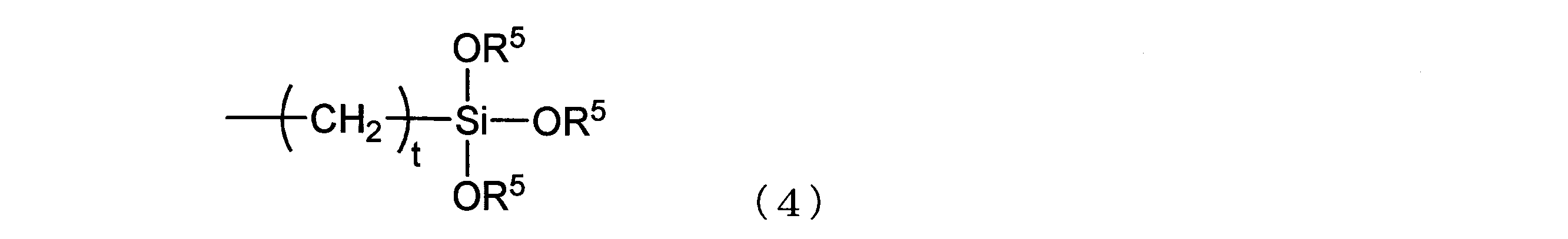
上記式(4)において、R4で示される酸素原子を有していてもよい一価脂肪族不飽和炭化水素基としては、好ましくは炭素数2~12、より好ましくは炭素数2~8、更に好ましくは炭素数2~6の、直鎖状又は分岐状のアルケニル基、例えば、ビニル基、アリル基、1-ブテニル基、1-ヘキセニル基、2-メチルプロペニル基や、(メタ)アクリル基等が挙げられる。例えば、下記式で表すことができる。
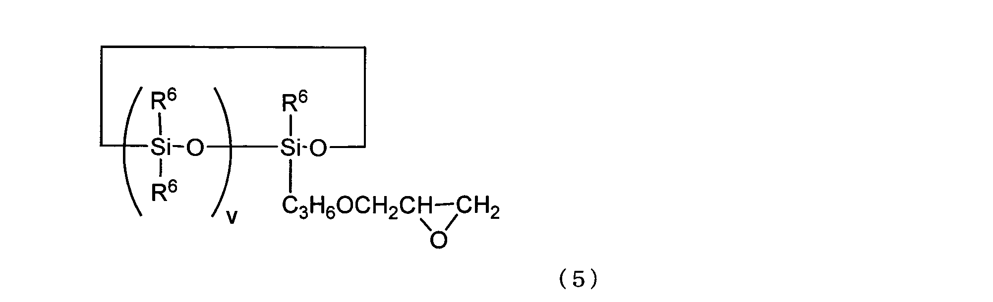
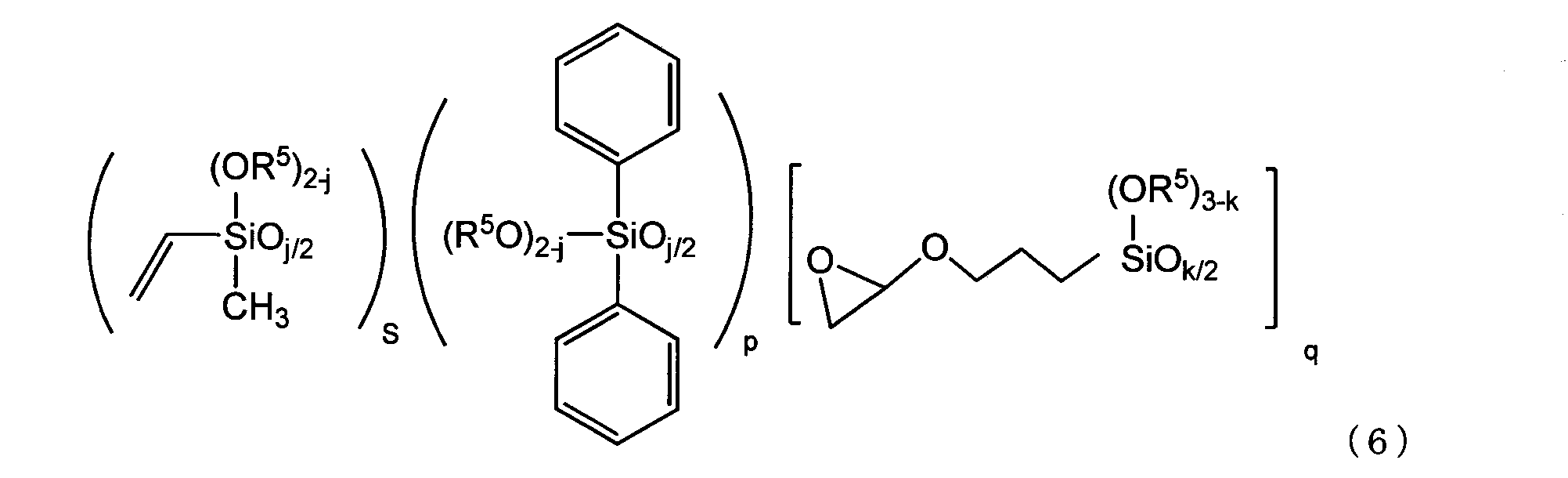
他の接着助剤としては、分子中にエポキシ基を少なくとも1つ有するオルガノポリシロキサンが挙げられる。該オルガノポリシロキサンは従来公知の化合物であればよい。例えば、下記一般式(5)又は平均式(6)で示されるオルガノシロキサンが挙げられる。中でも、下記一般式(5)で示される化合物を含む組成物は、硬化後の触媒膜との剥離性が他の接着助剤より良好であるため好ましい。
接着助剤を配合する場合の配合量は、(A)、(B)成分の合計100質量部に対して、10質量部以下が好ましく、より好ましくは0.1~8質量部、特に好ましくは0.2~5質量部である。配合量が上記上限値以下であれば硬化物硬度が高いものとなり、表面タック性も抑えられる。 When the adhesive auxiliary is blended, the blending amount is preferably 10 parts by mass or less, more preferably 0.1 to 8 parts by mass, and particularly preferably 0.1 parts by mass with respect to 100 parts by mass of the total of the components (A) and (B). It is 0.2 to 5 parts by mass. If the blending amount is not more than the above upper limit, the hardness of the cured product is high and the surface tackiness is suppressed.
また、接着助剤を配合する場合の配合量として、本接着助剤を含む全組成物中のアルケニル基の合計個数に対して、全組成物中のヒドロシリル基の合計個数の比が0.4~4となる量が好ましく、0.6~3となる量がより好ましく、0.8~2となる量が更に好ましい。 In addition, as the blending amount when the adhesive aid is blended, the ratio of the total number of hydrosilyl groups in the total composition to the total number of alkenyl groups in the total composition containing the present adhesive aid is 0.4. The amount of up to 4 is preferable, the amount of up to 0.6 to 3 is more preferable, and the amount of up to 0.8 to 2 is even more preferable.
更に(A)、(B)成分の合計100質量部に対して接着助剤成分の割合は0.01~10質量部であるのが好ましく、より好ましくは0.1~5質量部である。この範囲内であれば、本発明の効果を損なうことなく、接着力を向上することができる。 Further, the ratio of the adhesive auxiliary component to the total of 100 parts by mass of the components (A) and (B) is preferably 0.01 to 10 parts by mass, and more preferably 0.1 to 5 parts by mass. Within this range, the adhesive strength can be improved without impairing the effect of the present invention.
本発明のオルガノポリシロキサン組成物には、上述した(A)、(B)、(C)成分以外に、必要に応じて、蛍光体、無機充填材及び硬化抑制剤等を含有してもよい。以下、各成分について説明する。 In addition to the above-mentioned components (A), (B) and (C), the organopolysiloxane composition of the present invention may contain a fluorescent substance, an inorganic filler, a curing inhibitor and the like, if necessary. .. Hereinafter, each component will be described.
[蛍光体]
蛍光体は、特に制限されるものでなく、従来公知の蛍光体を使用すればよい。例えば、半導体素子、特に窒化物系半導体を発光層とする半導体発光ダイオードからの光を吸収し、異なる波長の光に波長変換するものであることが好ましい。このような蛍光体としては、例えば、Eu、Ce等のランタノイド系元素で主に賦活される窒化物系蛍光体・酸窒化物系蛍光体、Eu等のランタノイド系、Mn等の遷移金属系の元素により主に賦活されるアルカリ土類金属ハロゲンアパタイト蛍光体、アルカリ土類金属ホウ酸ハロゲン蛍光体、アルカリ土類金属アルミン酸塩蛍光体、アルカリ土類金属ケイ酸塩蛍光体、アルカリ土類金属硫化物蛍光体、アルカリ土類金属チオガレート蛍光体、アルカリ土類金属窒化ケイ素蛍光体、ゲルマン酸塩蛍光体、又は、Ce等のランタノイド系元素で主に賦活される希土類アルミン酸塩蛍光体、希土類ケイ酸塩蛍光体又はEu等のランタノイド系元素で主に賦活される有機及び有機錯体蛍光体、Ca-Al-Si-O-N系オキシ窒化物ガラス蛍光体等から選ばれる1種以上であることが好ましい。
[Fluorescent material]
The fluorescent substance is not particularly limited, and a conventionally known fluorescent substance may be used. For example, it is preferable to absorb light from a semiconductor element, particularly a semiconductor light emitting diode having a nitride semiconductor as a light emitting layer, and convert the wavelength into light having a different wavelength. Examples of such a phosphor include a nitride-based phosphor / oxynitride-based phosphor that is mainly activated by a lanthanoid-based element such as Eu and Ce, a lanthanoid-based phosphor such as Eu, and a transition metal-based such as Mn. Alkaline earth metal halogen apatite phosphors, alkaline earth metal boron borate phosphors, alkaline earth metal aluminate phosphors, alkaline earth metal silicate phosphors, alkaline earth metals mainly activated by elements Rare earth aluminate phosphors, rare earths that are mainly activated by sulfide phosphors, alkaline earth metal thiogalate phosphors, alkaline earth metal silicon nitride phosphors, germanate phosphors, or lanthanoid elements such as Ce. One or more selected from organic and organic complex phosphors mainly activated by silicate phosphors or lanthanoid elements such as Eu, Ca-Al-Si-ON oxynitride glass phosphors, and the like. Is preferable.
Eu、Ce等のランタノイド系元素で主に賦活される窒化物系蛍光体としては、M2Si5N8:Eu(Mは、Sr、Ca、Ba、Mg、Znから選ばれる少なくとも1種である。)が挙げられる。また、MSi7N10:Eu、M1.8Si5O0.2N8:Eu、及びM0.9Si7O0.1N10:Eu(Mは、Sr、Ca、Ba、Mg、Znから選ばれる少なくとも1種である。)などが挙げられる。 The nitride-based phosphor mainly activated by lanthanoid-based elements such as Eu and Ce is M 2 Si 5 N 8 : Eu (M is at least one selected from Sr, Ca, Ba, Mg and Zn. There is.). Further, MSi 7 N 10 : Eu, M 1.8 Si 5 O 0.2 N 8 : Eu, and M 0.9 Si 7 O 0.1 N 10 : Eu (M is at least one selected from Sr, Ca, Ba, Mg, Zn). It is.) And so on.
Eu、Ce等のランタノイド系元素で主に賦活される酸窒化物系蛍光体としては、MSi2O2N2:Eu(Mは、Sr、Ca、Ba、Mg、Znから選ばれる少なくとも1種である。)が挙げられる。 As the oxynitride-based phosphor mainly activated by lanthanoid-based elements such as Eu and Ce, at least one selected from MSi 2 O 2 N 2 : Eu (M is Sr, Ca, Ba, Mg, Zn). Is mentioned.).
Eu等のランタノイド系、Mn等の遷移金属系の元素により主に賦活されるアルカリ土類金属ハロゲンアパタイト蛍光体としては、M5(PO4)3X’:R’(Mは、Sr、Ca、Ba、Mg、Znから選ばれる少なくとも1種である。X’は、F、Cl、Br、Iから選ばれる少なくとも1種である。R’はEu及びMnのいずれか1以上である。)が挙げられる。 Alkaline earth metal halogen apatite phosphors mainly activated by lanthanoid-based elements such as Eu and transition metal-based elements such as Mn include M 5 (PO 4 ) 3 X': R'(M is Sr, Ca). , Ba, Mg, Zn. X'is at least one selected from F, Cl, Br, I. R'is one or more of Eu and Mn.) Can be mentioned.
アルカリ土類金属ホウ酸ハロゲン蛍光体としては、M2B5O9X’:R’(Mは、Sr、Ca、Ba、Mg、Znから選ばれる少なくとも1種である。X’は、F、Cl、Br、Iから選ばれる少なくとも1種である。R’はEu及びMnのいずれか1以上である。)が挙げられる。 The alkaline earth metal halide halogen phosphor is M 2 B 5 O 9 X': R'(M is at least one selected from Sr, Ca, Ba, Mg and Zn. X'is F. , Cl, Br, and at least one selected from I. R'is one or more of Eu and Mn).
アルカリ土類金属アルミン酸塩蛍光体としては、SrAl2O4:R’、Sr4Al14O25:R’、CaAl2O4:R’、BaMg2Al16O27:R’、BaMg2Al16O12:R’、及びBaMgAl10O17:R’(R’はEu及びMnのいずれか1以上である。)が挙げられる。 As alkaline earth metal aluminate phosphors, SrAl 2 O 4 : R', Sr 4 Al 14 O 25 : R', CaAl 2 O 4 : R', BaMg 2 Al 16 O 27 : R', BaMg 2 Examples thereof include Al 16 O 12 : R'and BaMgAl 10 O 17 : R'(R'is one or more of Eu and Mn).
アルカリ土類金属硫化物蛍光体としては、La2O2S:Eu、Y2O2S:Eu、及びGd2O2S:Euなどが挙げられる。 Examples of the alkaline earth metal sulfide phosphor include La 2 O 2 S: Eu, Y 2 O 2 S: Eu, and Gd 2 O 2 S: Eu.
Ce等のランタノイド系元素で主に賦活される希土類アルミン酸塩蛍光体としては、Y3Al5O12:Ce、(Y0.8Gd0.2)3Al5O12:Ce、Y3(Al0.8Ga0.2)5O12:Ce、及び(Y,Gd)3(Al,Ga)5O12の組成式で表されるYAG系蛍光体が挙げられる。また、Yの一部もしくは全部をTb、Lu等で置換したTb3Al5O12:Ce、Lu3Al5O12:Ceなどもある。 Rare earth aluminate phosphors mainly activated by lanthanoid elements such as Ce include Y 3 Al 5 O 12 : Ce, (Y 0.8 Gd 0.2 ) 3 Al 5 O 12 : Ce, Y 3 (Al 0.8 Ga). 0.2 ) 5 O 12 : A YAG-based phosphor represented by the composition formula of Ce and (Y, Gd) 3 (Al, Ga) 5 O 12 can be mentioned. Further, there are also Tb 3 Al 5 O 12 : Ce, Lu 3 Al 5 O 12 : Ce, etc. in which a part or all of Y is replaced with Tb, Lu, or the like.
その他の蛍光体には、ZnS:Eu、Zn2GeO4:Mn、MGa2S4:Eu(Mは、Sr、Ca、Ba、Mg、Znから選ばれる少なくとも1種である。)などが挙げられる。 Examples of other phosphors include ZnS: Eu, Zn 2 GeO 4 : Mn, Mga 2 S 4 : Eu (M is at least one selected from Sr, Ca, Ba, Mg, and Zn). Be done.
上記蛍光体は、所望に応じてEuに代えて、又は、Euに加えてTb、Cu、Ag、Au、Cr、Nd、Dy、Co、Ni、Tiから選択される1種以上を含有させることができる。 The above phosphor should contain at least one selected from Tb, Cu, Ag, Au, Cr, Nd, Dy, Co, Ni and Ti in place of Eu or in addition to Eu, if desired. Can be done.
Ca-Al-Si-O-N系オキシ窒化物ガラス蛍光体とは、モル%で、CaCO3をCaOに換算して20~50モル%、Al2O3を0~30モル%、SiOを25~60モル%、AlNを5~50モル%、希土類酸化物又は遷移金属酸化物を0.1~20モル%とし、5成分の合計が100モル%となるオキシ窒化物ガラスを母体材料とした蛍光体である。なお、オキシ窒化物ガラスを母体材料とした蛍光体では、窒素含有量が15モル%以下であることが好ましく、希土類酸化物イオンの他に増感剤となる他の希土類元素イオンを希土類酸化物として蛍光ガラス中に0.1~10モル%の範囲の含有量で共賦活剤として含むことが好ましい。 The Ca-Al-Si-ON-based oxynitride glass phosphor is mol%, CaCO 3 is converted into CaO, 20 to 50 mol%, Al 2 O 3 is 0 to 30 mol%, and SiO is The base material is oxynitride glass in which 25 to 60 mol%, AlN is 5 to 50 mol%, rare earth oxide or transition metal oxide is 0.1 to 20 mol%, and the total of the five components is 100 mol%. It is a phosphor. In a phosphor made of oxynitride glass as a base material, the nitrogen content is preferably 15 mol% or less, and in addition to rare earth oxide ions, other rare earth element ions serving as sensitizers are used as rare earth oxides. It is preferable to include the content in the fluorescent glass in the range of 0.1 to 10 mol% as a coactivator.
また、上記蛍光体以外の蛍光体であって、同様の性能、効果を有する蛍光体を使用することもできる。 Further, a fluorescent substance other than the above-mentioned fluorescent substance, which has the same performance and effect, can also be used.
本発明に用いる蛍光体は、平均粒径10nm以上を有することが好ましく、より好ましくは10nm~10μm、更に好ましくは10nm~1μmを有するのがよい。上記平均粒径は、シーラスレーザー測定装置などのレーザー光回折法による粒度分布測定で測定される。 The phosphor used in the present invention preferably has an average particle size of 10 nm or more, more preferably 10 nm to 10 μm, and even more preferably 10 nm to 1 μm. The average particle size is measured by measuring the particle size distribution by a laser light diffraction method such as a Cirrus laser measuring device.
蛍光体を配合する場合の配合量は、蛍光体以外の成分、例えば(A)及び(B)成分の合計100質量部に対して、0.1~2,000質量部が好ましく、より好ましくは0.1~100質量部である。本発明のオルガノポリシロキサン組成物の硬化物を蛍光体含有波長変換フィルムとする場合は、蛍光体の含有量を10~2,000質量部とするのが好ましい。 When the fluorescent substance is blended, the blending amount is preferably 0.1 to 2,000 parts by mass, more preferably 0.1 to 2,000 parts by mass, based on 100 parts by mass of the total of the components other than the fluorescent substance, for example, the components (A) and (B). It is 0.1 to 100 parts by mass. When the cured product of the organopolysiloxane composition of the present invention is used as a fluorophore-containing wavelength conversion film, the fluorophore content is preferably 10 to 2,000 parts by mass.
[無機充填材]
無機充填材としては、例えば、シリカ、ヒュームドシリカ、ヒュームド二酸化チタン、アルミナ、炭酸カルシウム、ケイ酸カルシウム、二酸化チタン、酸化第二鉄、及び酸化亜鉛等を挙げることができる。これらは、1種単独で又は2種以上を併せて使用することができる。
[Inorganic filler]
Examples of the inorganic filler include silica, fumed silica, fumed titanium dioxide, alumina, calcium carbonate, calcium silicate, titanium dioxide, ferrous oxide, zinc oxide and the like. These can be used alone or in combination of two or more.
無機充填材を配合する場合の配合量は特に制限されないが、本発明のシリコーン樹脂フィルムが透明性を失わない程度の量であることが好ましい。(A)及び(B)成分の合計100質量部あたり20質量部以下、好ましくは0.1~10質量部の範囲で適宜配合すればよい。 The blending amount when blending the inorganic filler is not particularly limited, but it is preferable that the blending amount is such that the silicone resin film of the present invention does not lose its transparency. 20 parts by mass or less, preferably 0.1 to 10 parts by mass, may be appropriately blended per 100 parts by mass of the components (A) and (B).
[その他の添加剤]
本発明のオルガノポリシロキサン組成物には、上記成分のほかに、その他の添加剤を配合することができる。その他の添加剤としては、例えば、ラジカル禁止剤、難燃剤、界面活性剤、光安定剤、増粘剤、可塑剤、酸化防止剤、熱安定剤、導電性付与剤、帯電防止剤、放射線遮断剤、核剤、リン系過酸化物分解剤、滑剤、顔料、金属不活性化剤、物性調整剤、有機溶剤等が挙げられる。これらの任意成分は、1種を単独で用いても2種以上を併用してもよい。
[Other additives]
In addition to the above components, other additives can be added to the organopolysiloxane composition of the present invention. Other additives include, for example, radical inhibitors, flame retardants, surfactants, light stabilizers, thickeners, plasticizers, antioxidants, heat stabilizers, conductivity-imparting agents, antistatic agents, radiation blocking agents. Examples thereof include agents, nucleating agents, phosphorus-based peroxide decomposing agents, lubricants, pigments, metal inactivating agents, physical property adjusting agents, organic solvents and the like. These optional components may be used alone or in combination of two or more.
本発明のオルガノポリシロキサン組成物の最も単純な実施形態は、(B)成分のみ、又は、(A)及び(B)成分からなる組成物である。なお、高い透明性を有する硬化物を得るためには、前記無機充填材を含有しないことが好ましい。本発明のオルガノポリシロキサン組成物の調製方法は特に制限されるものでなく、従来公知の方法に従えばよく、上記(A)、(B)成分、及びその他の任意成分を任意の方法により混合して調製すればよい。例えば、市販の攪拌機(THINKY CONDITIONING MIXER(株)シンキー製)等に入れて、1~5分間程度、均一に混合することによって調製することができる。 The simplest embodiment of the organopolysiloxane composition of the present invention is a composition consisting of only the component (B) or the components (A) and (B). In addition, in order to obtain a cured product having high transparency, it is preferable that the inorganic filler is not contained. The method for preparing the organopolysiloxane composition of the present invention is not particularly limited, and conventionally known methods may be followed, and the above components (A), (B), and other optional components may be mixed by any method. And prepare it. For example, it can be prepared by putting it in a commercially available stirrer (THINKY CONDITIONING MIXER Co., Ltd., manufactured by Shinky Co., Ltd.) and mixing it uniformly for about 1 to 5 minutes.
本発明のオルガノポリシロキサン組成物の性状は、液状、半固体状、固体状のいずれでもよいが、25℃で固体状であれば、硬化前でも樹脂の流動性が非常に低いため、硬化前後での形状維持が容易であり好ましい。 The properties of the organopolysiloxane composition of the present invention may be liquid, semi-solid, or solid, but if it is solid at 25 ° C, the fluidity of the resin is very low even before curing, so before and after curing. It is preferable because it is easy to maintain the shape of the product.
本発明のオルガノポリシロキサン組成物は、高い光透過性を有する硬化物を与えることができる。従って、本発明のオルガノポリシロキサン組成物は、LED素子封止用、特に青色LEDや紫外LEDの素子封止用として有用である。本発明のオルガノポリシロキサン組成物でLED素子等を封止する方法は従来公知の方法に従えばよい。例えば、ディスペンス法、及びコンプレッションモールド法などが使用できる。 The organopolysiloxane composition of the present invention can provide a cured product having high light transmittance. Therefore, the organopolysiloxane composition of the present invention is useful for encapsulating LED elements, particularly for encapsulating blue LEDs and ultraviolet LEDs. The method for sealing the LED element or the like with the organopolysiloxane composition of the present invention may follow a conventionally known method. For example, a dispense method, a compression mold method, and the like can be used.
[製造方法I.シリコーン樹脂フィルムの製造方法]
以下、シリコーン樹脂フィルムの製造方法について、さらに詳細に説明する。
本発明の製造方法I.は、下記工程(1)~(3)を含む。
(1)触媒活性を有する膜1枚の上にて、または2枚の間にて、前記オルガノポリシロキサン組成物を膜状に成形する工程、又は、膜状に成形したオルガノポリシロキサン組成物の少なくとも1面と触媒活性を有する膜とを貼り合わせる工程、
(2)次いで、前記オルガノポリシロキサン組成物を硬化してシリコーン樹脂フィルムを得る工程、及び
(3)得られたシリコーン樹脂フィルムと前記膜とを剥離する工程
[Manufacturing method I. Silicone resin film manufacturing method]
Hereinafter, the method for producing the silicone resin film will be described in more detail.
The manufacturing method of the present invention I. Includes the following steps (1) to (3).
(1) A step of forming the organopolysiloxane composition into a film, or an organopolysiloxane composition formed into a film, on or between two films having catalytic activity. A step of bonding at least one surface and a film having catalytic activity,
(2) Next, a step of curing the organopolysiloxane composition to obtain a silicone resin film, and (3) a step of peeling the obtained silicone resin film from the film.
製造方法I.の工程(1)
オルガノポリシロキサン組成物を膜状に成形する方法は、従来公知の方法に従えばよく、例えばフィルムコーター、熱プレス機等を使用することができる。フィルムコーターとしては、ダイレクトグラビアコーター、チャンバードクターコーター、オフセットグラビアコーター、ロールキスコーター、リバースキスコーター、バーコーター、ダイコーター、リバースロールコーター、スロットダイ、エアードクターコーター、正回転ロールコーター、ブレードコーター、ナイフコーター、含浸コーター、MBコーター、及びMBリバースコーターなどがある。中でもダイレクトグラビアコーター、オフセットグラビアコーター、ダイコーターなどが好ましい。熱プレス機を用いる場合は、触媒膜を貼り合せる工程が、組成物の成形前であっても成形後であってもよい。フィルムコーターを用いる場合は、フィルム状に成形した後に触媒膜を貼り合せることが好ましい。
Process of manufacturing method I. (1)
As a method for forming the organopolysiloxane composition into a film, a conventionally known method may be followed, and for example, a film coater, a heat press machine or the like can be used. Film coaters include direct gravure coater, chamber doctor coater, offset gravure coater, roll kiss coater, reverse kiss coater, bar coater, die coater, reverse roll coater, slot die, air doctor coater, forward rotation roll coater, blade coater, etc. There are knife coaters, impregnation coaters, MB coaters, and MB reverse coaters. Of these, direct gravure coaters, offset gravure coaters, die coaters and the like are preferable. When a hot press machine is used, the step of laminating the catalyst membrane may be before or after molding the composition. When a film coater is used, it is preferable to bond the catalyst film after molding into a film.
また、膜状に成形したオルガノポリシロキサン組成物の触媒膜が貼り合わされていない面に、更に、別の触媒膜を貼りあわせてもよい。 Further, another catalyst film may be further attached to the surface to which the catalyst film of the organopolysiloxane composition formed into a film is not attached.
膜状に成形するオルガノポリシロキサン組成物の厚さは、10~2,000μmが好ましく、さらには50~1,000μmがより好ましい。この範囲であれば、触媒膜が有する触媒によって組成物を十分に硬化することができ、硬化不良を起こすことがない。 The thickness of the organopolysiloxane composition formed into a film is preferably 10 to 2,000 μm, more preferably 50 to 1,000 μm. Within this range, the composition can be sufficiently cured by the catalyst contained in the catalyst membrane, and curing failure does not occur.
熱プレス機を用いる場合、通常60~150℃、好ましくは80~120℃の温度で、0.1~20MPa、好ましくは0.3~15MPaの圧力下で、1~40分間、好ましくは1~20分間圧縮成形を行う。オルガノポリシロキサン組成物の片面または両面に触媒膜を配置し、熱プレス機を用いて圧縮成形を行っても良い。熱プレス機を用いた場合の、フィルム成形厚さは、得られる硬化物の厚さとして0.01~3mm、好ましくは0.015~2mmである。 When a hot press is used, it is usually at a temperature of 60 to 150 ° C., preferably 80 to 120 ° C., and under a pressure of 0.1 to 20 MPa, preferably 0.3 to 15 MPa for 1 to 40 minutes, preferably 1 to 1 to 1. Perform compression molding for 20 minutes. A catalyst membrane may be arranged on one side or both sides of the organopolysiloxane composition, and compression molding may be performed using a hot press machine. When a hot press machine is used, the film forming thickness is 0.01 to 3 mm, preferably 0.015 to 2 mm as the thickness of the obtained cured product.
フィルムコーターを用いる場合は、無溶剤の状態でシート状等に成形してもよいが、該組成物を有機溶媒に溶解してワニスとしてもよい。 When a film coater is used, it may be formed into a sheet or the like in a solvent-free state, or the composition may be dissolved in an organic solvent to form a varnish.
前記有機溶媒としては、特に限定されないが、例えば、ベンゼン、トルエン、キシレン等の炭化水素系溶媒;テトラヒドロフラン、1,4-ジオキサン、ジエチルエーテル等のエーテル系溶媒;メチルエチルケトン等のケトン系溶媒;クロロホルム、塩化メチレン、1,2-ジクロロエタン等のハロゲン系溶媒;メタノール、エタノール、イソプロピルアルコール、イソブチルアルコール等のアルコール系溶媒;オクタメチルシクロテトラシロキサン、ヘキサメチルジシロキサン等が挙げられ、更にセロソルブアセテート、シクロヘキサノン、ブチロセロソルブ、メチルカルビトール、カルビトール、ブチルカルビトール、ジエチルカルビトール、シクロヘキサノール、ジグライム、トリグライムなどの溶剤である。これらの有機溶媒は、1種単独で用いても2種以上を併用してもよい。ワニス状態の組成物をフィルムコーターで60~150℃、好ましくは80~120℃の温度で1~20分間、好ましくは3~10分間加熱してシート状に加工する。フィルムコーターを用いた場合の、フィルム成形厚さは、得られる硬化物の厚さとして0.01~1mm、好ましくは0.015~0.5mmである。 The organic solvent is not particularly limited, and for example, a hydrocarbon solvent such as benzene, toluene, and xylene; an ether solvent such as tetrahydrofuran, 1,4-dioxane, and diethyl ether; a ketone solvent such as methyl ethyl ketone; chloroform, and the like. Halogen-based solvents such as methylene chloride, 1,2-dichloroethane; alcohol-based solvents such as methanol, ethanol, isopropyl alcohol and isobutyl alcohol; octamethylcyclotetrasiloxane, hexamethyldisiloxane and the like, and further, cellosolve acetate, cyclohexanone, etc. It is a solvent such as butyrocellosolve, methylcarbitol, carbitol, butylcarbitol, diethylcarbitol, cyclohexanol, diglime, and triglime. These organic solvents may be used alone or in combination of two or more. The varnished composition is heated with a film coater at a temperature of 60 to 150 ° C., preferably 80 to 120 ° C. for 1 to 20 minutes, preferably 3 to 10 minutes to process it into a sheet. When a film coater is used, the film forming thickness is 0.01 to 1 mm, preferably 0.015 to 0.5 mm as the thickness of the obtained cured product.
さらには、膜状に成形したオルガノポリシロキサン組成物の触媒膜が貼り合わされていない面に離型フィルムを貼り合せてもよい。離型フィルムとしてはフッ素系樹脂コートしたPETフィルム、シリコーン樹脂コートしたPETフィルム、フッ素系樹脂フィルムなどが挙げられる。 Further, the release film may be attached to the surface to which the catalyst film of the organopolysiloxane composition formed into a film is not attached. Examples of the release film include a PET film coated with a fluororesin, a PET film coated with a silicone resin, and a fluororesin film.
製造方法I.の工程(2)
本発明のオルガノポリシロキサン組成物の硬化条件は、脱水素縮合型及び付加反応硬化型のいずれも、特に制限されるものでなく、従来公知の方法に従えばよい。例えば、60~180℃、1~12時間程度で硬化することができる。特には、ステップキュアによって硬化させることが好ましい。ステップキュアでは、例えば以下の2段階を経て行うことができる。まず、オルガノポリシロキサン組成物を60~100℃の温度で0.5~2時間加熱し、十分に脱泡させる。次いで、オルガノポリシロキサン組成物を120~180℃の温度で1~10時間加熱硬化させる。これらの段階を経ることにより十分に硬化し、気泡の発生がなく、無色透明の硬化物を得ることができる。本発明において無色透明の硬化物とは、1mm厚での450nmにおける光透過率が80%以上、好ましくは85%以上、特に好ましくは90%以上であるものを意味する。
Process of manufacturing method I. (2)
The curing conditions of the organopolysiloxane composition of the present invention are not particularly limited to either the dehydrogenation condensation type or the addition reaction curing type, and conventionally known methods may be followed. For example, it can be cured at 60 to 180 ° C. for about 1 to 12 hours. In particular, it is preferable to cure by step curing. Step cure can be performed, for example, through the following two steps. First, the organopolysiloxane composition is heated at a temperature of 60 to 100 ° C. for 0.5 to 2 hours to sufficiently defoam. The organopolysiloxane composition is then heat-cured at a temperature of 120-180 ° C. for 1-10 hours. By going through these steps, it is sufficiently cured, no bubbles are generated, and a colorless and transparent cured product can be obtained. In the present invention, the colorless and transparent cured product means a product having a light transmittance of 80% or more, preferably 85% or more, particularly preferably 90% or more at 450 nm at a thickness of 1 mm.
製造方法I.の工程(3)
上記工程により形成された硬化物(シリコーン樹脂フィルム)と触媒膜とを剥離することにより、シリコーン樹脂フィルムを得ることができる。本発明の製造方法を用いれば、シリコーン樹脂フィルム中に含まれる金属触媒の量は金属質量換算で0.1ppm未満となり、好ましくは0.05ppm未満となる。上記上限値超になると、未硬化状態で組成物の保存安定性が低下し、また、得られるシリコーン樹脂フィルムの耐熱性及び信頼性も低下する恐れがあるため、好ましくない。
Process of manufacturing method I. (3)
A silicone resin film can be obtained by peeling off the cured product (silicone resin film) formed by the above step and the catalyst film. According to the production method of the present invention, the amount of the metal catalyst contained in the silicone resin film is less than 0.1 ppm in terms of metal mass, preferably less than 0.05 ppm. If it exceeds the above upper limit, the storage stability of the composition is lowered in the uncured state, and the heat resistance and reliability of the obtained silicone resin film may be lowered, which is not preferable.
[製造方法II.半導体デバイスの製造方法]
以下、本発明のオルガノポリシロキサン組成物からなる膜状成形物(硬化前の組成物からなる成形物を意味する)を用いた半導体デバイスの製造方法について、さらに詳細に説明する。
本発明の製造方法II.は、下記工程(1)~(4)を含む。
(1)触媒活性を有する膜1枚の上に、前記オルガノポリシロキサン組成物を膜状に成形する工程、又は、膜状に成形したオルガノポリシロキサン組成物の1面と触媒活性を有する膜とを貼り合わせて膜状積層物を得る工程
(2)前記工程(1)で得た膜状積層物の組成物面と、半導体チップが搭載された基板の半導体チップ搭載面とを貼り合せて、半導体チップを前記オルガノポリシロキサン組成物で被覆する工程
(3)前記オルガノポリシロキサン組成物を硬化する工程
(4)前記硬化物と前記触媒膜とを剥離して、前記硬化物で半導体チップが被覆された半導体デバイスを得る工程
さらに本発明の製造方法II.は前記工程(4)の後に(5)得られた半導体デバイスをダイシングし個片化する工程を更に含むことができる。
[Manufacturing method II. Manufacturing method of semiconductor device]
Hereinafter, a method for manufacturing a semiconductor device using the film-shaped molded product made of the organopolysiloxane composition of the present invention (meaning the molded product made of the uncured composition) will be described in more detail.
The production method of the present invention II. Includes the following steps (1) to (4).
(1) A step of forming the organopolysiloxane composition into a film on one film having catalytic activity, or one surface of the organopolysiloxane composition formed into a film and a film having catalytic activity. (2) The composition surface of the film-like laminate obtained in the above step (1) and the semiconductor chip mounting surface of the substrate on which the semiconductor chip is mounted are bonded together to obtain a film-like laminate. Step of coating the semiconductor chip with the organopolysiloxane composition (3) Step of curing the organopolysiloxane composition (4) The cured product and the catalyst film are peeled off, and the semiconductor chip is coated with the cured product. Step of obtaining the semiconductor device of the present invention Further, the manufacturing method of the present invention II. Can further include the step (5) after the step (4) of dicing and disassembling the obtained semiconductor device.
該製造方法II.による半導体デバイスの製造方法を説明するための模式図を図4に示す。図4に示される各工程(1)~(5)は上記工程(1)~(5)に対応している。以下、各工程をより詳細に説明する。
製造方法II.の工程(1)
工程(1)では、硬化性オルガノポリシロキサン組成物を膜状に成形し、該膜状成型物と触媒膜からなる膜状積層物を得る(図4の工程(1))。膜状に成形する方法及び触媒膜と張り付ける方法は、上記した製造方法I.の工程(1)に記載した通りである。
The manufacturing method II. FIG. 4 shows a schematic diagram for explaining a method of manufacturing a semiconductor device according to the above. Each step (1) to (5) shown in FIG. 4 corresponds to the above steps (1) to (5). Hereinafter, each step will be described in more detail.
Process of manufacturing method II. (1)
In the step (1), the curable organopolysiloxane composition is formed into a film, and a film-like laminate composed of the film-like molded product and the catalyst film is obtained (step (1) in FIG. 4). The method of forming into a film and the method of attaching to the catalyst film are described in the above-mentioned manufacturing method I. It is as described in the step (1) of.
製造方法II.の工程(2)
前記工程(1)で得た膜状積層物の組成物面と、半導体チップが搭載されている基板の半導体チップ搭載面とを貼り合せて、半導体チップを前記オルガノポリシロキサン組成物で被覆する(図4の工程(2))。該工程は従来公知の方法に従えばよく、熱プレスや真空ラミネータ、圧縮成形などが使用でき、特に追従性から真空ラミネータが望ましい。より詳細には、例えば、成型装置の上型の金属板上に粘着フィルムなどを介して半導体チップが搭載されている基板を粘着させ、成形装置の下型に前記積層物の触媒面を成形面側に載置し、真空ラミネータ(ニッコーマテリアルズ社製 V-130)にて、成形温度50~150℃、系内の真空度は0.1~10hPa、真空10秒~1分、押し込み圧力は0.05~0.5MPaで成形することができる。
Step of manufacturing method II. (2)
The composition surface of the film-like laminate obtained in the step (1) is bonded to the semiconductor chip mounting surface of the substrate on which the semiconductor chip is mounted, and the semiconductor chip is coated with the organopolysiloxane composition (the semiconductor chip is coated with the organopolysiloxane composition). Step (2) of FIG. The step may follow a conventionally known method, and a hot press, a vacuum laminator, compression molding, or the like can be used, and a vacuum laminator is particularly desirable from the viewpoint of followability. More specifically, for example, a substrate on which a semiconductor chip is mounted is adhered to a metal plate of an upper mold of a molding apparatus via an adhesive film or the like, and a catalyst surface of the laminate is formed on a lower mold of the molding apparatus. Placed on the side, with a vacuum laminator (V-130 manufactured by Nikko Materials), the molding temperature is 50 to 150 ° C, the degree of vacuum in the system is 0.1 to 10 hPa, the vacuum is 10 seconds to 1 minute, and the pushing pressure is It can be molded at 0.05 to 0.5 MPa.
製造方法II.の工程(3)
前記工程(2)で得られるオルガノポリシロキサン組成物で半導体チップが被覆された半導体デバイスを硬化する(図4の工程(3))。
Process of manufacturing method II. (3)
The semiconductor device in which the semiconductor chip is coated with the organopolysiloxane composition obtained in the step (2) is cured (step (3) in FIG. 4).
本発明の硬化性オルガノポリシロキサン組成物の硬化条件は、上記した製造方法I.の工程(2)に記載した通りである。例えば、60~180℃の温度で、1~12時間加熱して硬化することができる。好ましくは120~180℃、1~4時間で加熱するのがよい。特には、ステップキュアによって硬化させることが好ましい。ステップキュアについては上述した通りである。180℃超の硬化温度(例えば200℃)で長時間(例えば4時間以上)加熱すると、得られる硬化物と触媒膜との剥離が容易でなくなる恐れがある。本発明のオルガノポリシロキサン組成物からなる膜状成型物と触媒膜とからなる膜状積層物の組成物面と半導体デバイスとを貼りあわせることにより、ボイドの発生等を起こさずに成形できる。本発明の製造方法は、図2に示すようなフリップチップ型の半導体デバイス及び図3に示すようなワイヤ付きチップを有する半導体デバイスのどちらでも成形することができる。 The curing conditions of the curable organopolysiloxane composition of the present invention are the above-mentioned production method I. It is as described in the step (2) of. For example, it can be cured by heating at a temperature of 60 to 180 ° C. for 1 to 12 hours. It is preferable to heat at 120 to 180 ° C. for 1 to 4 hours. In particular, it is preferable to cure by step curing. The step cure is as described above. When heated at a curing temperature of more than 180 ° C. (for example, 200 ° C.) for a long time (for example, 4 hours or more), the obtained cured product and the catalyst membrane may not be easily peeled off. By laminating the composition surface of the film-like molded product made of the organopolysiloxane composition of the present invention and the film-like laminate made of the catalyst film and the semiconductor device, molding can be performed without causing voids or the like. The manufacturing method of the present invention can be formed by either a flip-chip type semiconductor device as shown in FIG. 2 or a semiconductor device having a wire-attached chip as shown in FIG.
製造方法II.の工程(4)
前記工程(3)にて得られた半導体デバイスにおいて硬化物と触媒膜とを剥離して、半導体チップが硬化物で被覆された半導体デバイスを得る(図4の工程(4))。本発明のオルガノポリシロキサン組成物の硬化物と触媒膜とは容易に手で剥離することができる。
Step of manufacturing method II. (4)
In the semiconductor device obtained in the step (3), the cured product and the catalyst membrane are peeled off to obtain a semiconductor device in which the semiconductor chip is coated with the cured product (step (4) in FIG. 4). The cured product of the organopolysiloxane composition of the present invention and the catalyst membrane can be easily peeled off by hand.
製造方法II.の工程(5)
工程(5)では上記工程で製造された半導体デバイスをパッケージとするためにダイシングして個片化する(図4の工程(5))。ダイシングはDISCO社製のダイサーなどで、バリなど発生することなくダイシングすることができる。
Step of manufacturing method II. (5)
In the step (5), the semiconductor device manufactured in the above step is diced and individualized in order to package it (step (5) in FIG. 4). Dicing is a dicing machine manufactured by DISCO, etc., and dicing can be performed without generating burrs.
本発明の製造方法を用いれば、上記した通り、硬化物中に含まれる金属触媒の量は金属質量換算で0.1ppm未満となり、好ましくは0.05ppm未満となるため耐熱性及び信頼性に優れた半導体デバイスを提供することができる。 When the production method of the present invention is used, as described above, the amount of the metal catalyst contained in the cured product is less than 0.1 ppm in terms of metal mass, preferably less than 0.05 ppm, and thus has excellent heat resistance and reliability. Can provide semiconductor devices.
以下、合成例、実施例及び比較例を示し、本発明をより詳細に説明するが、本発明は下記の実施例に制限されるものではない。 Hereinafter, the present invention will be described in more detail with reference to synthesis examples, examples and comparative examples, but the present invention is not limited to the following examples.
下記実施例において重量平均分子量は、ゲルパーミエーションクロマトグラフィ(GPC)によるポリスチレンを標準物質とした重量平均分子量である。測定条件は以下の通り。
[測定条件]
展開溶媒:THF
流量:0.6mL/min
検出器:示差屈折率検出器(RI)
カラム:TSK Guardcolomn SuperH-L
TSKgel SuperH4000(6.0mmI.D.×15cm×1)
TSKgel SuperH3000(6.0mmI.D.×15cm×1)
TSKgel SuperH2000(6.0mmI.D.×15cm×2)
(いずれも東ソー社製)
カラム温度:40℃
試料注入量:20μL(濃度0.5重量%のTHF溶液)
In the following examples, the weight average molecular weight is the weight average molecular weight using polystyrene as a standard material by gel permeation chromatography (GPC). The measurement conditions are as follows.
[Measurement condition]
Developing solvent: THF
Flow rate: 0.6 mL / min
Detector: Differential Refractometer Detector (RI)
Column: TSK Guardcolomn SuperH-L
TSKgel SuperH4000 (6.0mm ID x 15cm x 1)
TSKgel SuperH3000 (6.0mm ID x 15cm x 1)
TSKgel SuperH2000 (6.0 mm ID x 15 cm x 2)
(Both manufactured by Tosoh)
Column temperature: 40 ° C
Sample injection volume: 20 μL (THF solution with a concentration of 0.5 wt%)
[合成例1]
アルケニル基含有オルガノポリシロキサンの合成
フェニルトリクロロシラン1142.1g(87.1mol%)、ClMe2SiO(Me2SiO)33SiMe2Cl 529g(3.2mol%)、及びジメチルビニルクロロシラン72.4g(9.7mol%)をトルエン溶剤に溶解後、水中に滴下し、共加水分解し、更に水洗、アルカリ洗浄にて中和、脱水後、溶剤をストリップし、25℃で固体状のフェニル基含有ビニルシリコーンレジンA1を得た。THFを溶媒として用いたGPC測定によるポリスチレン換算の重量平均分子量は63,000であった。
[Synthesis Example 1]
Synthesis of alkenyl group-containing organopolysiloxane
Phenyltrichlorosilane 1142.1 g (87.1 mol%), ClMe 2 SiO (Me 2 SiO) 33 Sime 2 Cl 529 g (3.2 mol%), and dimethylvinylchlorosilane 72.4 g (9.7 mol%) as a toluene solvent After dissolution, it was dropped into water, co-hydrolyzed, neutralized by washing with water and washed with alkali, dehydrated, and then stripped of the solvent to obtain a solid phenyl group-containing vinyl silicone resin A1 at 25 ° C. The polystyrene-equivalent weight average molecular weight measured by GPC using THF as a solvent was 63,000.
[合成例2]
アルケニル基含有オルガノポリシロキサンの合成
フェニルトリクロロシラン1142.1g(84.4mol%)、ClMe2SiO(Me2SiO)13SiMe2Cl 466.6g(6.3mol%)、及びジメチルビニルクロロシラン72.4g(9.4mol%)をトルエン溶剤に溶解後、水中に滴下し、共加水分解し、更に水洗、アルカリ洗浄にて中和、脱水後、溶剤をストリップし、25℃で固体状のフェニル基含有ビニルシリコーンレジンA2を得た。THFを溶媒として用いたGPC測定によるポリスチレン換算の重量平均分子量は22,000であった。
[Synthesis Example 2]
Synthesis of alkenyl group-containing organopolysiloxane
Toluene phenyltrichlorosilane 1142.1 g (84.4 mol%), ClMe 2 SiO (Me 2 SiO) 13 Sime 2 Cl 466.6 g (6.3 mol%), and dimethylvinylchlorosilane 72.4 g (9.4 mol%). After being dissolved in a solvent, it was dropped into water, co-hydrolyzed, neutralized by washing with water and washed with alkali, dehydrated, and then stripped of the solvent to obtain a solid phenyl group-containing vinyl silicone resin A2 at 25 ° C. The polystyrene-equivalent weight average molecular weight measured by GPC using THF as a solvent was 22,000.
[合成例3]
アルケニル基含有オルガノポリシロキサンの合成
フェニルトリクロロシラン1142.1g(87.4mol%)、HO-(PhMeSiO)35-H 869.7g(2.9mol%)、及びジメチルビニルクロロシラン72.3g(9.7mol%)をトルエン溶剤に溶解後、水中に滴下し、共加水分解し、更に水洗、アルカリ洗浄にて中和、脱水後、溶剤をストリップし、25℃で固体状のフェニル基含有ビニルシリコーンレジンA3を得た。THFを溶媒として用いたGPC測定によるポリスチレン換算の重量平均分子量は23,000であった。
[Synthesis Example 3]
Synthesis of alkenyl group-containing organopolysiloxane
After dissolving 1142.1 g (87.4 mol%) of phenyltrichlorosilane, HO- (PhMeSiO) 35 -H 869.7 g (2.9 mol%), and 72.3 g (9.7 mol%) of dimethylvinylchlorosilane in a toluene solvent. , Dropped into water, co-hydrolyzed, neutralized by washing with water and washed with alkali, dehydrated, and then stripped of the solvent to obtain a solid phenyl group-containing vinyl silicone resin A3 at 25 ° C. The polystyrene-equivalent weight average molecular weight measured by GPC using THF as a solvent was 23,000.
[合成例4]
オルガノハイドロジェンポリシロキサンの合成
フェニルトリクロロシラン1142.1g(87.1mol%)、ClMe2SiO(Me2SiO)33SiMe2Cl 529g(3.2mol%)、及びメチルジクロロシラン69g(9.7mol%)をトルエン溶剤に溶解後、水中に滴下し、共加水分解し、更に水洗、アルカリ洗浄にて中和、脱水後、溶剤をストリップし、25℃で固体状のフェニル基含有ハイドロジェンシリコーンレジンB1を得た。THFを溶媒として用いたGPC測定によるポリスチレン換算の重量平均分子量は58,000であった。
[Synthesis Example 4]
Synthesis of Organohydrogen Polysiloxane
After dissolving 1142.1 g (87.1 mol%) of phenyltrichlorosilane, 529 g (3.2 mol%) of ClMe 2 SiO (Me 2 SiO) 33 , and 69 g (9.7 mol%) of methyldichlorosilane in a toluene solvent. , Dropped into water, co-hydrolyzed, neutralized by washing with water and washed with alkali, dehydrated, and then stripped of the solvent to obtain a solid phenyl group-containing hydrogen silicone resin B1 at 25 ° C. The polystyrene-equivalent weight average molecular weight measured by GPC using THF as a solvent was 58,000.
[合成例5]
オルガノハイドロジェンポリシロキサンの合成
フェニルトリクロロシラン1142.1g(84.4mol%)、ClMe2SiO(Me2SiO)13SiMe2Cl 466.6g(6.3mol%)、及びメチルジクロロシラン69.0g(9.4mol%)をトルエン溶剤に溶解後、水中に滴下し、共加水分解し、更に水洗、アルカリ洗浄にて中和、脱水後、溶剤をストリップし、25℃で固体状のフェニル基含有ハイドロジェンシリコーンレジンB2を得た。THFを溶媒として用いたGPC測定によるポリスチレン換算の重量平均分子量は11,000であった。
[Synthesis Example 5]
Synthesis of Organohydrogen Polysiloxane
Toluene phenyltrichlorosilane 1142.1 g (84.4 mol%), ClMe 2 SiO (Me 2 SiO) 13 Sime 2 Cl 466.6 g (6.3 mol%), and methyldichlorosilane 69.0 g (9.4 mol%). After being dissolved in a solvent, it was dropped into water, co-hydrolyzed, neutralized by washing with water and washed with alkali, dehydrated, and then stripped of the solvent to obtain a solid phenyl group-containing hydrogen silicone resin B2 at 25 ° C. .. The polystyrene-equivalent weight average molecular weight measured by GPC using THF as a solvent was 11,000.
[合成例6]
オルガノハイドロジェンポリシロキサンの合成
フェニルトリクロロシラン1142.1g(87.4mol%)、HO-(PhMeSiO)35-H 869.7g(2.9mol%)、及びメチルジクロロシラン69g(9.7mol%)をトルエン溶剤に溶解後、水中に滴下し、共加水分解し、更に水洗、アルカリ洗浄にて中和、脱水後、溶剤をストリップし、25℃で固体状のフェニル基含有ハイドロジェンシリコーンレジンB3を得た。THFを溶媒として用いたGPC測定によるポリスチレン換算の重量平均分子量は8,000であった。
[Synthesis Example 6]
Synthesis of Organohydrogen Polysiloxane
After dissolving 1142.1 g (87.4 mol%) of phenyltrichlorosilane, HO- (PhMeSiO) 35 -H 869.7 g (2.9 mol%), and 69 g (9.7 mol%) of methyldichlorosilane in a toluene solvent, It was dropped into water, co-hydrolyzed, neutralized by washing with water and washed with alkali, dehydrated, and then stripped of the solvent to obtain a solid phenyl group-containing hydrogen silicone resin B3 at 25 ° C. The polystyrene-equivalent weight average molecular weight measured by GPC using THF as a solvent was 8,000.
[触媒膜]
下記実施例において使用した触媒膜は、無機酸化物/ポリビニルアルコールハイブリッド化合物にパラジウムを固定した触媒膜(商品名:Pd-iObrane(登録商標)、ニッポン高度紙工業株式会社製、Pd担持量 7wt%)である。
[Catalyst membrane]
The catalyst film used in the following examples is a catalyst film in which palladium is immobilized on an inorganic oxide / polyvinyl alcohol hybrid compound (trade name: Pd-iObrane (registered trademark), manufactured by Nippon Kodoshi Kogyo Co., Ltd., Pd loading amount 7 wt%. ).
I.シリコーン樹脂フィルムの製造
[実施例1]
合成例1で合成したビニルシリコーンレジンA1を100g、合成例4で合成したハイドロジェンシリコーンレジンB1を100g混合して、オルガノポリシロキサン組成物1を調製した。自動塗工装置 PI-1210(テスター産業(株)社製)を用いて、触媒膜Pd-iObrane(登録商標)の上に該オルガノポリシロキサン組成物1を塗布し、縦150mm×横150mm及び厚さ0.1mmを有する膜状に成形した(成形物F1)。
I. Production of Silicone Resin Film [Example 1]
100 g of the vinyl silicone resin A1 synthesized in Synthesis Example 1 and 100 g of the hydrogen silicone resin B1 synthesized in Synthesis Example 4 were mixed to prepare an
[実施例2]
合成例2で合成したビニルシリコーンレジンA2を100gと、合成例5で合成したハイドロジェンシリコーンレジンB2を100gとを混合してオルガノポリシロキサン組成物2を調製した。オルガノポリシロキサン組成物1に変えてオルガノポリシロキサン組成物2を用いた他は実施例1を繰り返し、縦150mm×横150mm及び厚さ0.1mmを有する膜状に成形した(成形物F2)。
[Example 2]
An
[実施例3]
合成例3で合成したビニルシリコーンレジンA3を100gと、合成例6で合成したハイドロジェンシリコーンレジンB3を100gとを混合してオルガノポリシロキサン組成物3を調製した。オルガノポリシロキサン組成物1に変えてオルガノポリシロキサン組成物3を用いた他は実施例1を繰り返し、縦150mm×横150mm及び厚さ0.1mmを有する膜状に成形した(成形物F3)。
[Example 3]
An
[実施例4]
合成例1で合成したビニルシリコーンレジンA1を100gと、合成例4で合成したハイドロジェンシリコーンレジンB1を100gと、および下記式(3’)で表される接着付与剤2を6gとを混合して、オルガノポリシロキサン組成物4を調製した。オルガノポリシロキサン組成物1に変えてオルガノポリシロキサン組成物4を用いた他は実施例1を繰り返し、縦150mm×横150mm及び厚さ0.1mmを有する膜状に成形した(成形物F4)。
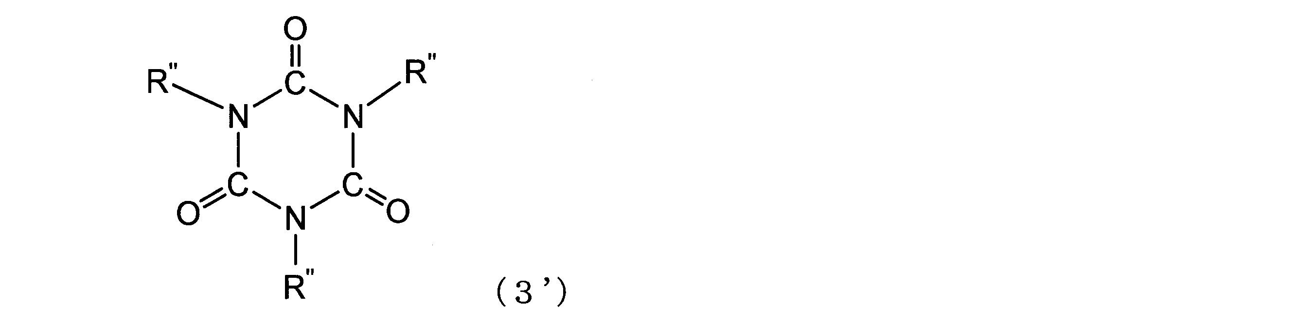
100 g of the vinyl silicone resin A1 synthesized in the synthesis example 1, 100 g of the hydrogen silicone resin B1 synthesized in the synthesis example 4, and 6 g of the adhesive-imparting
[実施例5]
合成例2で合成したビニルシリコーンレジンA2を100gと、合成例5で合成したハイドロジェンシリコーンレジンB2を100gと、上記式(3’)で表される接着付与剤6gとを混合して、オルガノポリシロキサン組成物5を調製した。オルガノポリシロキサン組成物1に変えてオルガノポリシロキサン組成物5を用いた他は実施例1を繰り返し、縦150mm×横150mm及び厚さ0.1mmを有する膜状に成形した(成形物F5)。
[Example 5]
100 g of the vinyl silicone resin A2 synthesized in Synthesis Example 2, 100 g of the hydrogen silicone resin B2 synthesized in Synthesis Example 5, and 6 g of the adhesion-imparting agent represented by the above formula (3') are mixed to form an organo
[実施例6]
合成例3で合成したビニルシリコーンレジンA3を100gと、合成例6で調製したハイドロジェンシリコーンレジンB3を100gと、および上記式(3’)で表される接着付与剤6gとを混合して、オルガノポリシロキサン組成物6を調製した。オルガノポリシロキサン組成物1に変えてオルガノポリシロキサン組成物6を用いた他は実施例1を繰り返し、縦150mm×横150mm及び厚さ0.1mmを有する膜状に成形した(成形物F6)。
[Example 6]
100 g of the vinyl silicone resin A3 synthesized in Synthesis Example 3, 100 g of the hydrogen silicone resin B3 prepared in Synthesis Example 6, and 6 g of the adhesion-imparting agent represented by the above formula (3') are mixed.
[実施例7]
塗布したオルガノポリシロキサン組成物の厚さを0.4mmに変えた他は上記実施例1を繰り返し、縦150mm×横150mm、厚さ0.4mmを有する膜状に成形した(成形物F7)。
[Example 7]
Except for changing the thickness of the applied organopolysiloxane composition to 0.4 mm, the above-mentioned Example 1 was repeated to form a film having a length of 150 mm × a width of 150 mm and a thickness of 0.4 mm (molded product F7).
[実施例8]
2枚の触媒膜Pd-iObrane(登録商標)で実施例1で調製したオルガノポリシロキサン組成物1を挟み、圧縮成形して、縦150mm×横150mm、厚さ0.1mmを有する膜状に成形した。該膜状成形物 10枚について、一枚ずつ片側の触媒膜を剥離し加圧式真空ラミネータ V130(ニチゴー・モートン株式会社製)を用いて温度80℃で貼りあわせる工程を繰り返して10枚の成形物をラミネートして、両面に触媒膜を有する1.0mmの膜状成形物F8を製造した。
後述する評価試験においては、片方の面の触媒膜を剥離して、成形物をスライドガラスに貼り合せた。
[Example 8]
The
In the evaluation test described later, the catalyst film on one side was peeled off and the molded product was attached to the slide glass.
[実施例9]
実施例1で調製したオルガノポリシロキサン組成物1を用い、パラジウムナノ粒子担持ポリビニルアルコールフィルムの代わりにPETフィルムを用いた他は実施例1を繰り返し、縦150mm×横150mm、厚さ0.1mmを有する膜状に成形した。該膜状成形物 10枚について、PETフィルムを剥離して、加圧式真空ラミネータ V130(ニチゴー・モートン株式会社製)を用いて貼りあわせ、温度80℃でラミネートして、得られた成形物の片面にあるPETフィルムを剥離して触媒膜Pd-iObraneを貼り付けた。片面に触媒膜を有し、もう一方の面にPETフィルムを有する1.0mmの膜状成形物F9を製造した。
[Example 9]
Example 1 was repeated except that the
[比較例1]
合成例1で合成したビニルシリコーンレジンA1を100g、合成例4で合成したハイドロジェンシリコーンレジンB1を100g、ヒドロシリル化反応触媒として塩化白金酸のビニルシリコーン変性溶液(白金濃度1質量%)0.2g、反応抑制剤としてアセチレンアルコール系のエチニルシクロヘキサノール0.6g、接着付与剤として上記式(3’)で表される接着付与剤6.0gを混合して、オルガノポリシロキサン組成物C’1を調製した。自動塗工装置 PI-1210(テスター産業(株)社製)を用いて、PETフィルムの上に該オルガノポリシロキサン組成物C’1を塗布し、縦150mm×横150mm及び厚さ0.1mmを有する膜状に成形した(成形物F’1)。
[Comparative Example 1]
100 g of vinyl silicone resin A1 synthesized in Synthesis Example 1, 100 g of hydrogen silicone resin B1 synthesized in Synthesis Example 4, 0.2 g of vinyl silicone modified solution of platinum chloride acid (
[比較例2]
比較例1において、ヒドロシリル化反応触媒の量を0.004gとし、エチニルシクロヘキサノールの量を0.006gとした以外は比較例1を繰り返して、縦150mm×横150mm及び厚さ0.1mmを有する膜状に成形した(成形物F’2)。
[Comparative Example 2]
In Comparative Example 1, Comparative Example 1 was repeated except that the amount of the hydrosilylation reaction catalyst was 0.004 g and the amount of ethynylcyclohexanol was 0.006 g, and the hydrosilylation reaction catalyst had a length of 150 mm × a width of 150 mm and a thickness of 0.1 mm. It was molded into a film (molded product F'2).
[比較例3]
ビニルシリコーンレジンA1に替えてビニルシリコーンレジンA2を100g、ハイドロジェンシリコーンレジンB1に替えてハイドロジェンシリコーンレジンB2を100g用いた以外は比較例1を繰り返して、縦150mm×横150mm及び厚さ0.1mmを有する膜状に成形した(成形物F’3)。
[Comparative Example 3]
Comparative Example 1 was repeated except that 100 g of vinyl silicone resin A2 was used instead of vinyl silicone resin A1 and 100 g of hydrogen silicone resin B2 was used instead of hydrogen silicone resin B1, and the length was 150 mm × width 150 mm and the thickness was 0. It was molded into a film having 1 mm (molded product F'3).
[比較例4]
ビニルシリコーンレジンA1に替えてビニルシリコーンレジンA3を100g、ハイドロジェンシリコーンレジンB1に替えてハイドロジェンシリコーンレジンB3を100g用いた以外は比較例1を繰り返して、縦150mm×横150mm及び厚さ0.1mmを有する膜状に成形した(成形物F’4)。
[Comparative Example 4]
Comparative Example 1 was repeated except that 100 g of vinyl silicone resin A3 was used instead of vinyl silicone resin A1 and 100 g of hydrogen silicone resin B3 was used instead of hydrogen silicone resin B1, and the length was 150 mm × width 150 mm and the thickness was 0. It was molded into a film having 1 mm (molded product F'4).
[比較例5]
自動塗工装置 PI-1210(テスター産業(株)社製)を用いて、PETフィルムの上に実施例1で調製したオルガノポリシロキサン組成物1を塗布し、膜状に成形した。組成物は加熱すると溶融し、従来の形状を維持することができなかった。
[Comparative Example 5]
The
[比較例6]
自動塗工装置 PI-1210(テスター産業(株)社製)を用いて、PETフィルムの上に実施例2で調製したオルガノポリシロキサン組成物2を塗布し、膜状に成形した。組成物は加熱すると溶融し、従来の形状を維持することができなかった。
[Comparative Example 6]
The
[比較例7]
自動塗工装置 PI-1210(テスター産業(株)社製)を用いて、PETフィルムの上に実施例3で調製したオルガノポリシロキサン組成物3を塗布し、膜状に成形した。組成物は加熱すると溶融し、従来の形状を維持することができなかった。
[Comparative Example 7]
The
[比較例8]
比較例1で成形した成形物F’1 10枚について、PETフィルムを剥離して、加圧式真空ラミネータ V130(ニチゴー・モートン株式会社製)を用いて貼りあわせ、温度80℃でラミネートし、1.0mmの膜状成形物F’8を製造した。
[Comparative Example 8]
The PET film was peeled off from 10 pieces of the molded product F'1 molded in Comparative Example 1, bonded together using a pressurized vacuum laminator V130 (manufactured by Nichigo Morton Co., Ltd.), laminated at a temperature of 80 ° C., and 1. A 0 mm film-shaped molded product F'8 was produced.
[金属触媒残存量の測定]
実施例1~8、比較例1~7で形成した成形物について、各々、触媒膜が貼り合わされていない面をスライドガラスに貼り合わせて、150℃で4時間加熱して硬化させた。その後、硬化物から触媒膜を剥離してフィルムを得た。各フィルムについて、ICP-AES(高周波誘導結合プラズマ-発光分光分析法)を用いて、硬化物中に残存する金属触媒量を測定した。結果は表1及び2に記載の通りである。
[Measurement of residual metal catalyst]
For the molded products formed in Examples 1 to 8 and Comparative Examples 1 to 7, the surfaces to which the catalyst film was not bonded were bonded to a slide glass, and the molded products were heated at 150 ° C. for 4 hours to be cured. Then, the catalyst membrane was peeled off from the cured product to obtain a film. For each film, the amount of metal catalyst remaining in the cured product was measured using ICP-AES (Inductively Coupled Plasma-Emission Spectroscopy). The results are shown in Tables 1 and 2.
[微小硬度の測定]
実施例1~8、比較例1~7で形成した成形物について、各々、触媒膜が貼り合わされていない面をスライドガラスに貼り合わせて、150℃で4時間加熱して硬化させた。その後、硬化物から触媒膜を剥離してフィルムを得た。各フィルムについて、ダイナミック超微小硬度計 SHIMADZU DUH-211SR((株)島津製作所製)を用いて、負荷・除荷試験を行った。試験力1gf、負荷速度0.0298gf/秒、負荷および除荷保持時間各2秒の後、微小硬度(MPa)を測定した。試験回数5回の平均の微小硬度(MPa)を表1及び2に記載する。
[Measurement of minute hardness]
For the molded products formed in Examples 1 to 8 and Comparative Examples 1 to 7, the surfaces to which the catalyst film was not bonded were bonded to a slide glass, and the molded products were heated at 150 ° C. for 4 hours to be cured. Then, the catalyst membrane was peeled off from the cured product to obtain a film. Each film was subjected to a load / unloading test using a dynamic ultrafine hardness tester SHIMADZU DUH-211SR (manufactured by Shimadzu Corporation). After a test force of 1 gf, a load rate of 0.0298 gf / sec, and a load and unloading holding time of 2 seconds each, the minute hardness (MPa) was measured. The average micro-hardness (MPa) of 5 tests is shown in Tables 1 and 2.
[耐熱性試験(透過率変化)]
実施例1~8、及び比較例1~7で形成した成形物について、各々、触媒膜が貼り合わされていない面をスライドガラスに貼り合わせて、150℃で4時間加熱して硬化させた。その後、硬化物から触媒膜を剥離してフィルムを得た。該フィルムの400nmにおける透過率をJIS R 3106:1998に準拠して測定した(初期透過率)。次いで、該フィルムを180℃下に1000時間おいた後に、透過率を測定した。初期透過率を100%としたときの透過率(%)を算出した。
透過率変化(%)=(180℃×1,000時間放置後の透過率)/(初期透過率)
結果は表1及び2に記載の通りである。
[Heat resistance test (change in transmittance)]
For the molded products formed in Examples 1 to 8 and Comparative Examples 1 to 7, the surfaces to which the catalyst film was not bonded were bonded to a slide glass, and the molded products were heated at 150 ° C. for 4 hours to be cured. Then, the catalyst membrane was peeled off from the cured product to obtain a film. The transmittance of the film at 400 nm was measured according to JIS R 3106: 1998 (initial transmittance). Then, the film was placed at 180 ° C. for 1000 hours, and then the transmittance was measured. The transmittance (%) when the initial transmittance was 100% was calculated.
Transmittance change (%) = (180 ° C x transmittance after leaving for 1,000 hours) / (initial transmittance)
The results are shown in Tables 1 and 2.
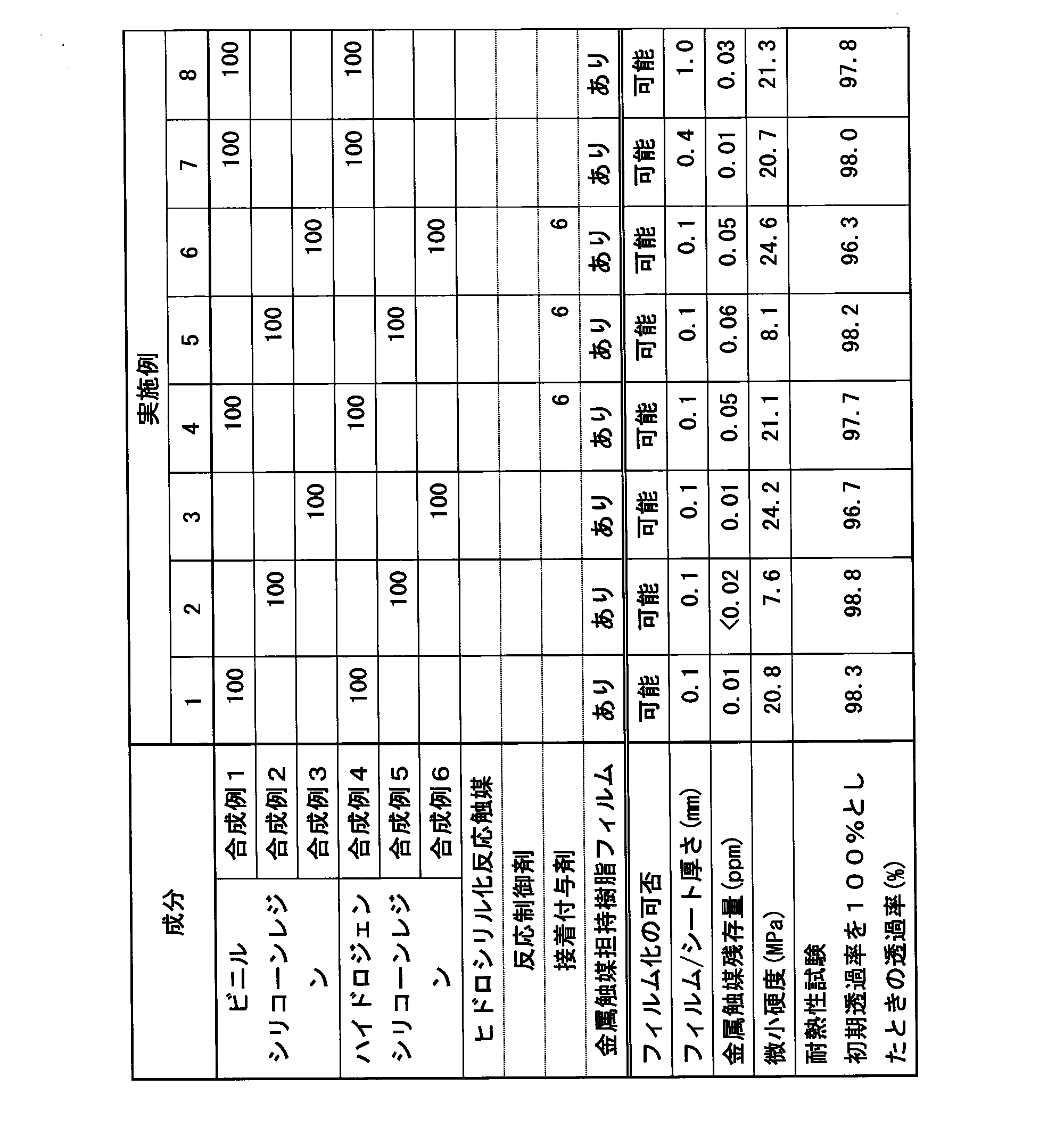
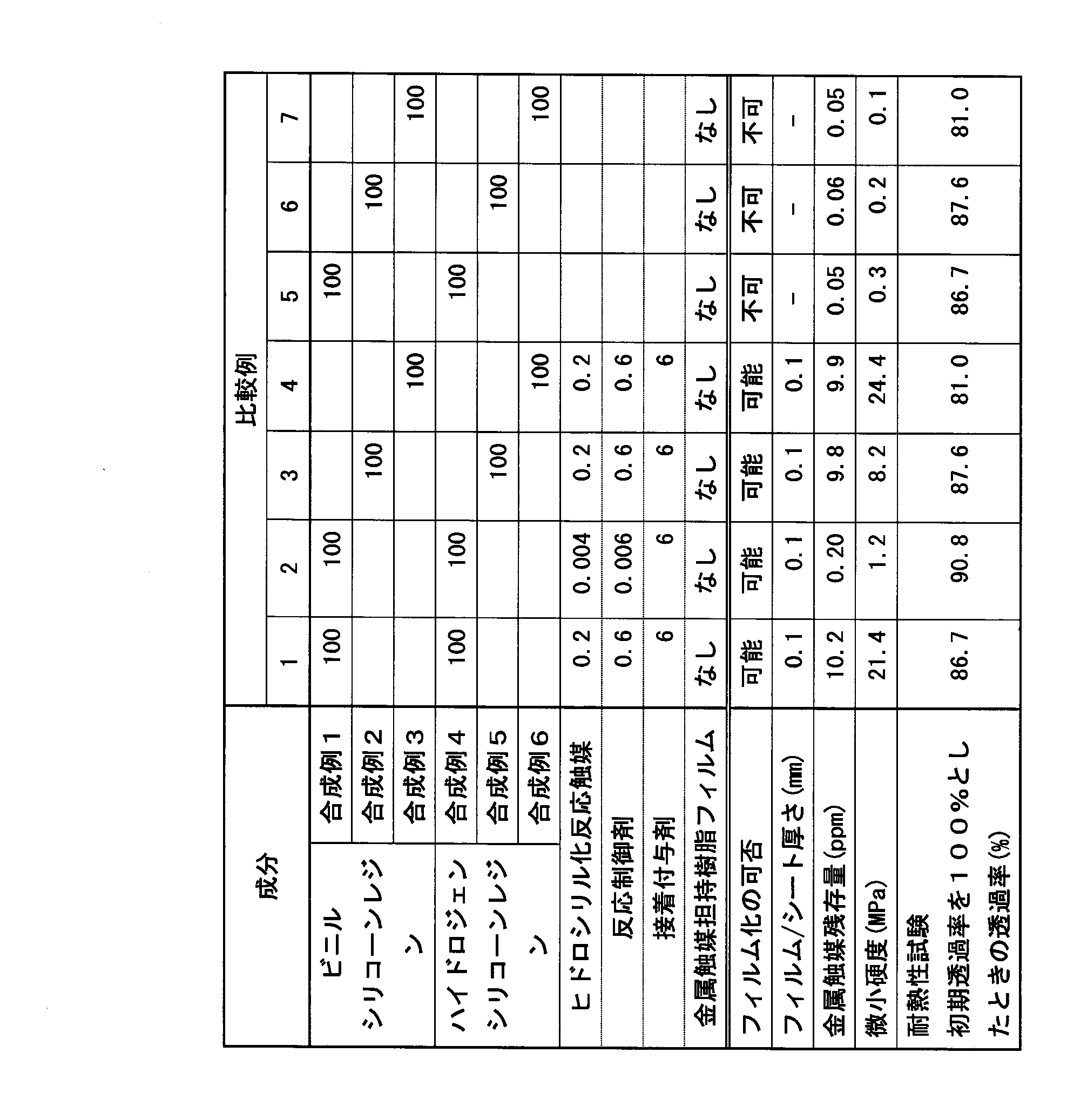
[長期保存安定性試験]
実施例9及び比較例8の成形物について、ダイナミック超微小硬度計 SHIMADZU DUH-211SR((株)島津製作所製)を用いて、負荷・除荷試験を行った。試験力1gf、負荷速度0.0298gf/秒、負荷および除荷保持時間各2秒の後、微小硬度(MPa)を測定した。試験回数5回の平均の微小硬度(MPa)を表3に記載する(硬化前の微小硬度(初期値))。次いで、実施例9及び比較例8の成形物を25℃で6ヶ月間保管した。保管後の成形物について、上記と同じく負荷・除荷試験を行い、平均微小硬度(MPa)を測定した(硬化前の微小硬度(保管後))。また、保管前と保管後のそれぞれの成形物を150℃4時間で加熱硬化してフィルムを製造し、硬化後の微小硬度を測定した。結果は表3に記載の通りである。
[Long-term storage stability test]
The molded products of Example 9 and Comparative Example 8 were subjected to a load / unloading test using a dynamic ultrafine hardness tester SHIMADZU DUH-211SR (manufactured by Shimadzu Corporation). After a test force of 1 gf, a load rate of 0.0298 gf / sec, and a load and unloading holding time of 2 seconds each, the minute hardness (MPa) was measured. The average micro-hardness (MPa) of 5 tests is shown in Table 3 (micro-hardness before curing (initial value)). Then, the molded articles of Example 9 and Comparative Example 8 were stored at 25 ° C. for 6 months. The molded product after storage was subjected to a loading / unloading test in the same manner as described above, and the average micro-hardness (MPa) was measured (micro-hardness before curing (after storage)). Further, each molded product before and after storage was heat-cured at 150 ° C. for 4 hours to produce a film, and the micro-hardness after curing was measured. The results are shown in Table 3.
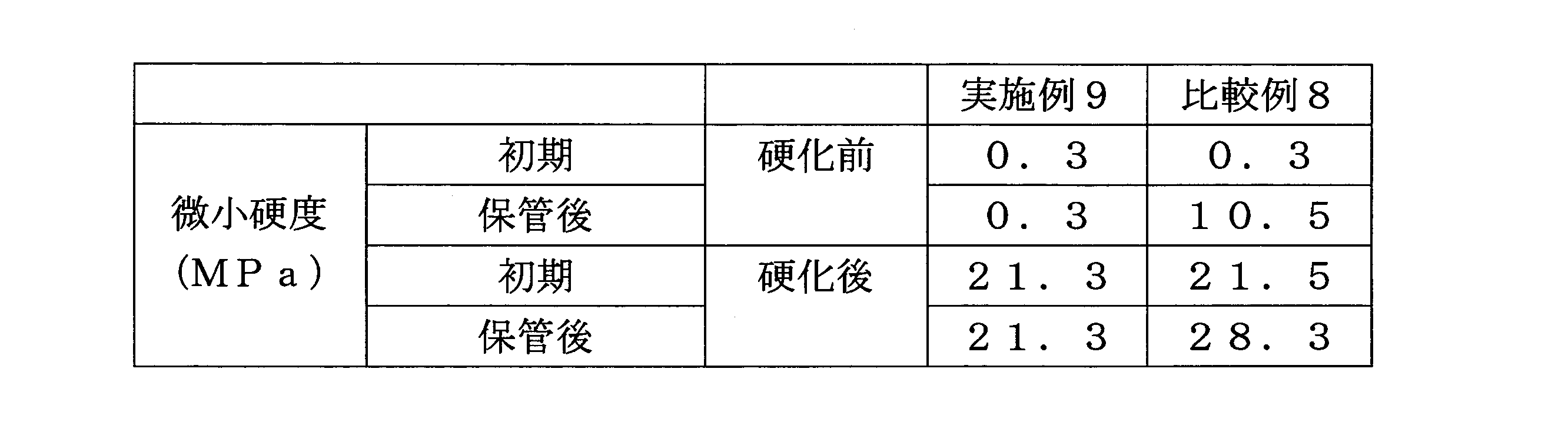
表1~3に示すように、触媒を含まないオルガノポリシロキサン組成物を、触媒膜を用いて硬化して得られるシリコーン樹脂フィルムは、透明であり、耐熱性にすぐれる。また、オルガノポリシロキサン組成物を触媒膜上に成形したものは未硬化の状態で長期間保管しても経時変化が起こりにくく、長期保存安定性に優れる。 As shown in Tables 1 to 3, the silicone resin film obtained by curing an organopolysiloxane composition containing no catalyst using a catalyst membrane is transparent and has excellent heat resistance. Further, the organopolysiloxane composition molded on the catalyst membrane does not easily change with time even if it is stored for a long period of time in an uncured state, and is excellent in long-term storage stability.
II.半導体デバイスの製造
[実施例10]
実施例1と同じオルガノポリシロキサン組成物1を調製した。自動塗工装置 PI-1210(テスター産業(株)社製)を用いて、触媒膜Pd-iObrane(登録商標)(図1の符号1)の上に該オルガノポリシロキサン組成物1(図1の符号2)を塗布し、縦×横×厚さ=100mm×100mm×0.2mmを有する膜状に成形した。該膜状の成形物と触媒膜からなる積層物の模式図を図1に示す。加圧式真空ラミネータ V130(ニチゴー・モートン株式会社製)を用いて、膜状積層物の組成物面(図2の符号2)と、半導体チップ搭載基板(半導体チップ(図2の符号3)は500μm×500μmを有し、高さ150μmを有するフリップチップ型LEDチップ、基板(図2の符号4)の大きさは10cm×10cm)とを貼り合わせた(該工程の模式図を図2に示す)。次いで、触媒膜を剥離させずに150℃×4時間加熱して、オルガノポリシロキサン組成物1を硬化させた。硬化後、硬化物と触媒膜とを剥離し、半導体チップが膜状硬化物で被覆された半導体デバイスを得た。該工程において硬化物と触媒膜層とは容易に剥離した。該半導体デバイスをダイシングして、縦3.5mm×横3.5mmを有し、厚さ0.2mmの硬化物で半導体チップが封止された半導体デバイスを得た(半導体デバイス1)。
II. Manufacturing of Semiconductor Devices [Example 10]
The
[実施例11]
実施例2と同じオルガノポリシロキサン組成物2を調製した。オルガノポリシロキサン組成物1に変えてオルガノポリシロキサン組成物2を用いた他は実施例10と同じ方法を繰り返して、縦3.5mm×横3.5mmを有し、厚さ0.2mmの硬化物で半導体チップが封止された半導体デバイスを得た(半導体デバイス2)。
[Example 11]
The
[実施例12]
実施例3と同じオルガノポリシロキサン組成物3を調製した。オルガノポリシロキサン組成物1に変えてオルガノポリシロキサン組成物3を用いた他は実施例10と同じ方法を繰り返して、縦3.5mm×横3.5mmを有し、厚さ0.2mmの硬化物で半導体チップが封止された半導体デバイスを得た(半導体デバイス3)。
[Example 12]
The
[実施例13]
合成例1で合成したビニルシリコーンレジンA1を100gと、合成例4で合成したハイドロジェンシリコーンレジンB1を100gと、および下記式(5’)

The vinyl silicone resin A1 synthesized in Synthesis Example 1 was 100 g, the hydrogen silicone resin B1 synthesized in Synthesis Example 4 was 100 g, and the following formula (5').
[実施例14]
合成例2で合成したビニルシリコーンレジンA2を100gと、合成例5で合成したハイドロジェンシリコーンレジンB2を100gと、上記式(5’)で表される接着助剤1を2g混合して、オルガノポリシロキサン組成物8を調製した。オルガノポリシロキサン組成物1に変えてオルガノポリシロキサン組成物8を用いた他は実施例10と同じ方法を繰り返して、縦3.5mm×横3.5mmを有し、厚さ0.2mmの硬化物で半導体チップが封止された半導体デバイスを得た(半導体デバイス5)。
[Example 14]
100 g of the vinyl silicone resin A2 synthesized in the synthesis example 2, 100 g of the hydrogen silicone resin B2 synthesized in the synthesis example 5, and 2 g of the
[実施例15]
合成例3で合成したビニルシリコーンレジンA3を100gと、合成例6で調製したハイドロジェンシリコーンレジンB3を100gと、および上記式(5’)で表される接着助剤1を2g混合して、オルガノポリシロキサン組成物9を調製した。オルガノポリシロキサン組成物1に変えてオルガノポリシロキサン組成物9を用いた他は実施例10と同じ方法を繰り返して、縦3.5mm×横3.5mmを有し、厚さ0.2mmの硬化物で半導体チップが封止された半導体デバイスを得た(半導体デバイス6)。
[Example 15]
100 g of the vinyl silicone resin A3 synthesized in Synthesis Example 3, 100 g of the hydrogen silicone resin B3 prepared in Synthesis Example 6, and 2 g of the
[実施例16]
上記実施例6において式(3’)で表される接着助剤2の量を2gにした他は実施例6を繰り返してオルガノポリシロキサン組成物10を調製した。オルガノポリシロキサン組成物1に変えてオルガノポリシロキサン組成物10を用いた他は実施例10と同じ方法を繰り返して、縦3.5mm×横3.5mmを有し、厚さ0.2mの硬化物で半導体チップが封止された半導体デバイスを得た(半導体デバイス7)。
[Example 16]
The organopolysiloxane composition 10 was prepared by repeating Example 6 except that the amount of the
[実施例17]
合成例3で合成したビニルシリコーンレジンA3を100gと、合成例6で調製したハイドロジェンシリコーンレジンB3を100gと、および下記平均式(6’)で表される接着助剤3を2g混合して、オルガノポリシロキサン組成物11を調製した。オルガノポリシロキサン組成物1に変えてオルガノポリシロキサン組成物11を用いた他は実施例10と同じ方法を繰り返して、縦3.5mm×横3.5mmを有し、厚さ0.2mmの硬化物で半導体チップが封止された半導体デバイスを得た(半導体デバイス8)。
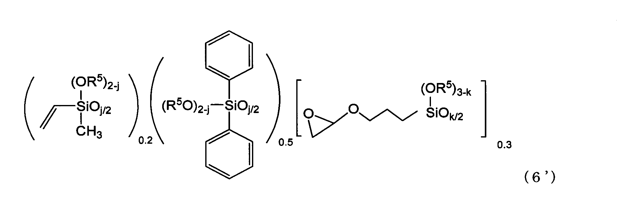
A mixture of 100 g of the vinyl silicone resin A3 synthesized in Synthesis Example 3, 100 g of the hydrogen silicone resin B3 prepared in Synthesis Example 6, and 2 g of the
[実施例18]
塗布したオルガノポリシロキサン組成物の厚さを0.4mmに変えた他は上記実施例10と同じ方法を繰り返して、縦3.5mm×横3.5mmを有し、厚さ0.4mmの硬化物で半導体チップが封止された半導体デバイスを得た(半導体デバイス9)。
[Example 18]
The same method as in Example 10 above was repeated except that the thickness of the applied organopolysiloxane composition was changed to 0.4 mm, and the film had a length of 3.5 mm × a width of 3.5 mm and was cured to a thickness of 0.4 mm. A semiconductor device in which a semiconductor chip was sealed with an object was obtained (semiconductor device 9).
[実施例19]
実施例10において半導体チップ搭載基板を、ワイヤ付きの半導体チップ搭載基板(半導体チップは500μm×500μm、高さ150μmを有するLEDチップ(ワイヤ付き)であり、ワイヤ高さは250μmであり、基板の大きさは10cm×10cmである。図3に模式図を示す)に替えた他は、実施例10と同じ方法を繰り返して、縦3.5mm×横3.5mmを有し、厚さ0.4mmの硬化物で半導体チップが封止された半導体デバイスを得た(半導体デバイス10)。
[Example 19]
In Example 10, the semiconductor chip mounting substrate is a semiconductor chip mounting substrate with a wire (the semiconductor chip is an LED chip (with a wire) having a height of 500 μm × 500 μm, and the wire height is 250 μm, and the size of the substrate is large. The size is 10 cm × 10 cm. A schematic diagram is shown in FIG. 3), and the same method as in Example 10 is repeated to have a length of 3.5 mm × a width of 3.5 mm and a thickness of 0.4 mm. A semiconductor device in which a semiconductor chip was sealed with the cured product of the above was obtained (semiconductor device 10).
[実施例20]
実施例10において、160℃×4時間で加熱する1段階の硬化条件を、100℃×1時間で加熱し、次いで、150℃×4時間加熱する2段階硬化に替えた他は、実施例10と同じ方法を繰り返して、縦3.5mm×横3.5mmを有し、厚さ0.2mmの硬化物で半導体チップが封止された半導体デバイスを得た(半導体デバイス11)。
[Example 20]
In Example 10, the one-step curing condition of heating at 160 ° C. × 4 hours was changed to the two-step curing condition of heating at 100 ° C. × 1 hour and then heating at 150 ° C. × 4 hours. By repeating the same method as above, a semiconductor device having a length of 3.5 mm and a width of 3.5 mm and having a semiconductor chip sealed with a cured product having a thickness of 0.2 mm was obtained (semiconductor device 11).
[比較例9]
合成例1で合成したビニルシリコーンレジンA1を100g、合成例4で合成したハイドロジェンシリコーンレジンB1を100g、ヒドロシリル化反応触媒として塩化白金酸のビニルシリコーン変性溶液(白金濃度1質量%)0.2g、反応抑制剤としてアセチレンアルコール系のエチニルシクロヘキサノール0.6g、接着付与剤として上記式(5’)で表される接着付与剤2gを混合して、オルガノポリシロキサン組成物C’2を調製した。自動塗工装置 PI-1210(テスター産業(株)社製)を用いて、PETフィルムの上に該オルガノポリシロキサン組成物C’2を塗布し、縦×横×厚さ=100mm×100mm×0.2mmを有する膜状に成形した。加圧式真空ラミネータ V130(ニチゴー・モートン株式会社製)を用いて、該膜状成形物の組成物面と実施例10と同じ半導体チップ搭載基板とを貼りあわせた。PETフィルムを剥離させ、150℃×4時間で加熱してオルガノポリシロキサン組成物C’2を硬化させた。得られた半導体デバイスをダイシングして、縦3.5mm×横3.5mmを有し、厚さ0.2mmの硬化物で半導体チップが封止された半導体デバイスを得た(半導体デバイス1’)。
[Comparative Example 9]
100 g of vinyl silicone resin A1 synthesized in Synthesis Example 1, 100 g of hydrogen silicone resin B1 synthesized in Synthesis Example 4, 0.2 g of vinyl silicone modified solution of platinum chloride acid (
[比較例10]
比較例9において、ヒドロシリル化反応触媒の量を0.004gとし、エチニルシクロヘキサノールの量を0.006gとした以外は比較例9と同じ方法を繰り返して、縦3.5mm×横3.5mmを有し、厚さ0.2mmの硬化物で半導体チップが封止された半導体デバイスを得た(半導体デバイス2’)。
[Comparative Example 10]
In Comparative Example 9, the same method as in Comparative Example 9 was repeated except that the amount of the hydrosilylation reaction catalyst was 0.004 g and the amount of ethynylcyclohexanol was 0.006 g, and the length was 3.5 mm × the width was 3.5 mm. A semiconductor device having a semiconductor chip sealed with a cured product having a thickness of 0.2 mm was obtained (semiconductor device 2').
[比較例11]
ビニルシリコーンレジンA1に替えてビニルシリコーンレジンA2を100g、ハイドロジェンシリコーンレジンB1に替えてハイドロジェンシリコーンレジンB2を100g用いた以外は比較例9と同じ方法を繰り返して、縦3.5mm×横3.5mmを有し、厚さ0.2mmの硬化物で半導体チップが封止された半導体デバイスを得た(半導体デバイス3’)。
[Comparative Example 11]
The same method as in Comparative Example 9 was repeated except that 100 g of vinyl silicone resin A2 was used instead of vinyl silicone resin A1 and 100 g of hydrogen silicone resin B2 was used instead of hydrogen silicone resin B1. A semiconductor device having a thickness of 0.5 mm and having a semiconductor chip sealed with a cured product having a thickness of 0.2 mm was obtained (semiconductor device 3').
[比較例12]
ビニルシリコーンレジンA1に替えてビニルシリコーンレジンA3を100g、ハイドロジェンシリコーンレジンB1に替えてハイドロジェンシリコーンレジンB3を100g用いた以外は比較例9と同じ方法を繰り返して、縦3.5mm×横3.5mmを有し、厚さ0.2mmの硬化物で半導体チップが封止された半導体デバイスを得た(半導体デバイス4’)。
[Comparative Example 12]
The same method as in Comparative Example 9 was repeated except that 100 g of vinyl silicone resin A3 was used instead of vinyl silicone resin A1 and 100 g of hydrogen silicone resin B3 was used instead of hydrogen silicone resin B1. A semiconductor device having a thickness of 0.5 mm and having a semiconductor chip sealed with a cured product having a thickness of 0.2 mm was obtained (semiconductor device 4').
[比較例13]
自動塗工装置 PI-1210(テスター産業(株)社製)を用いて、PETフィルムの上に実施例10で調製したオルガノポリシロキサン組成物1を塗布し、膜状に成形した。組成物は加熱すると溶融し、加熱前の形状を維持することができなかった。このため、以後の評価を行わなかった。
[Comparative Example 13]
The
[比較例14]
合成例1で合成したビニルシリコーンレジンA1を100g、合成例4で合成したハイドロジェンシリコーンレジンB1を100g、ヒドロシリル化反応触媒として塩化白金酸のビニルシリコーン変性溶液(白金濃度1質量%)0.2g、反応抑制剤としてアセチレンアルコール系のエチニルシクロヘキサノール0.6gを混合して、オルガノポリシロキサン組成物C’3を調製した。触媒膜Pd-iObrane(登録商標)の上に該オルガノポリシロキサン組成物C’3を塗布した他は比較例9の方法を繰り返し、縦3.5mm×横3.5mmを有し、厚さ0.2mmの膜状硬化物で半導体チップが封止された半導体デバイスを得た(半導体デバイス5’)。
[Comparative Example 14]
100 g of the vinyl silicone resin A1 synthesized in Synthesis Example 1, 100 g of the hydrogen silicone resin B1 synthesized in Synthesis Example 4, and 0.2 g of a vinyl silicone modified solution of platinum chloride acid (
実施例13~17の各々と同じ方法でオルガノポリシロキサン組成物7~11を調製した。自動塗工装置 PI-1210(テスター産業(株)社製)を用いて、触媒膜Pd-iObrane(登録商標)の上に各オルガノポリシロキサン組成物を塗布し、縦100mm×横100mmを有し、厚さ0.2mmを有する膜状に成形した。該膜状成形物を硬化し、触媒膜を剥離して得られるフィルムについて、金属触媒残存量の測定、微小硬度の測定、及び耐熱性試験(透過率変化)を行った。各試験方法は上記した通りである。結果を表4に示す。 Organopolysiloxane compositions 7-11 were prepared in the same manner as in each of Examples 13-17. Each organopolysiloxane composition is coated on the catalyst membrane Pd-iObrane (registered trademark) using an automatic coating device PI-1210 (manufactured by Tester Sangyo Co., Ltd.), and has a length of 100 mm and a width of 100 mm. , Formed into a film having a thickness of 0.2 mm. The film obtained by curing the film-like molded product and peeling off the catalyst film was subjected to measurement of the residual amount of the metal catalyst, measurement of the minute hardness, and heat resistance test (change in transmittance). Each test method is as described above. The results are shown in Table 4.

[触媒膜からの剥離性]
オルガノポリシロキサン組成物1~3及び7~11について触媒膜との剥離性を評価した。
上記実施例10~17の各々と同じ方法に従い、触媒膜Pd-iObrane(登録商標)の上に各オルガノポリシロキサン組成物を塗布し、膜状に成形した。触媒膜が貼り合わされていない面をスライドガラスに貼り合わせて、150℃×4時間で加熱硬化した。その後、硬化物から触媒膜を剥離した。オルガノポリシロキサン組成物1~3及び7~9から得られた硬化物は触媒膜から極めて容易に剥離することができ触媒膜上にシリコーン膜が残らなかった。オルガノポリシロキサン組成物10及び11から得られた硬化物は前者に比べると剥離性がやや劣るものの触媒膜から容易に剥離することはできた。
[Removability from catalyst membrane]
The releasability of the
Each organopolysiloxane composition was applied onto the catalyst film Pd-iObrane (registered trademark) according to the same method as in each of Examples 10 to 17, and molded into a film shape. The surface to which the catalyst membrane was not bonded was bonded to a slide glass and cured by heating at 150 ° C. for 4 hours. Then, the catalyst membrane was peeled off from the cured product. The cured products obtained from the
実施例10~20及び比較例9~12及び14で製造した半導体デバイスについて、以下の方法に従い耐熱性試験(輝度変化)を行った。結果を表5及び6に示す。
[耐熱性試験(輝度変化)]
各半導体デバイスについて、HTOL試験(高温駆動試験 試験条件180℃、印加電流500mA)を1,000時間おいた後に、初期との輝度変化を測定した。初期輝度を100%としたときの輝度(%)を下記式により算出した。
輝度変化(%)=(180℃×1,000時間放置後の輝度)/(初期輝度)
The semiconductor devices manufactured in Examples 10 to 20 and Comparative Examples 9 to 12 and 14 were subjected to a heat resistance test (luminance change) according to the following method. The results are shown in Tables 5 and 6.
[Heat resistance test (change in brightness)]
For each semiconductor device, after an HTOL test ( high temperature drive test test condition 180 ° C., applied current 500 mA) was allowed for 1,000 hours, the change in brightness from the initial stage was measured. The brightness (%) when the initial brightness was 100% was calculated by the following formula.
Luminance change (%) = (180 ° C x brightness after leaving for 1,000 hours) / (initial brightness)
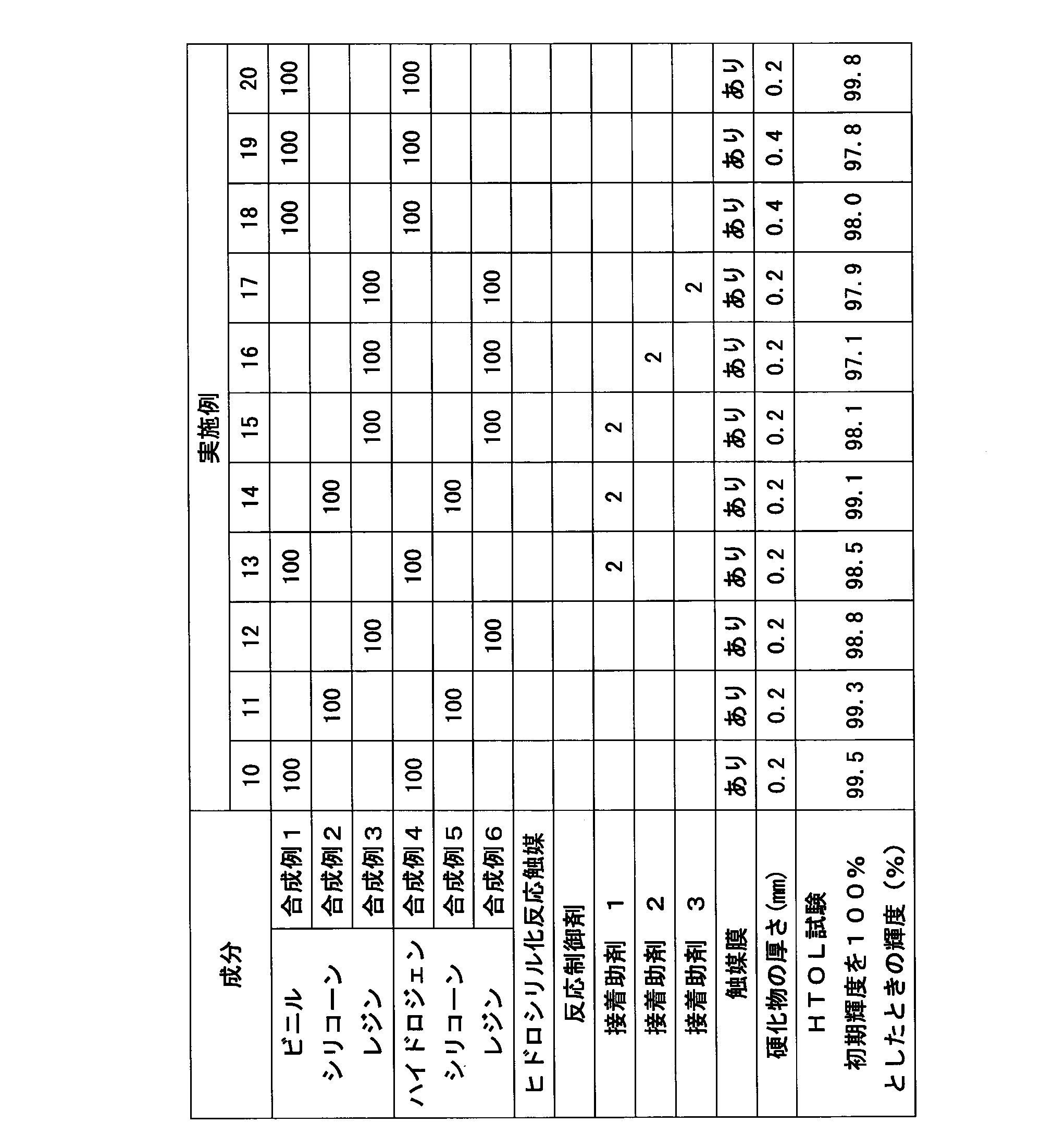
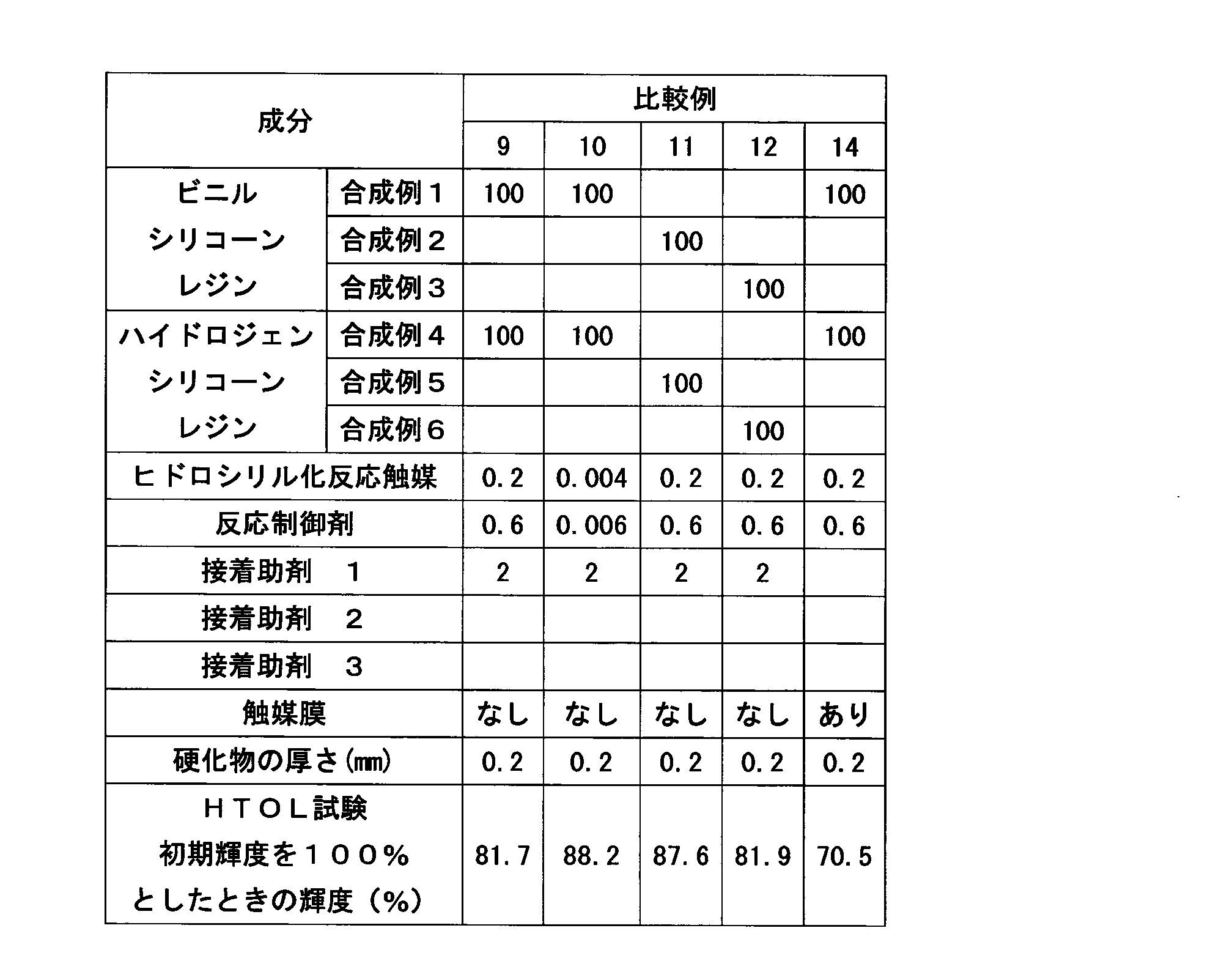
表5に示す通り、本発明の製造方法に従い触媒を含まないオルガノポリシロキサン組成物の硬化物からなる膜状物で半導体チップを封止することにより、得られる半導体デバイスは耐熱性に優れる。 As shown in Table 5, the semiconductor device obtained by encapsulating the semiconductor chip with a film-like material made of a cured product of an organopolysiloxane composition containing no catalyst according to the production method of the present invention has excellent heat resistance.
本発明の製造方法は、耐熱性及び透過性にすぐれ、長期間保管しても経時変化が起こりにくく、信頼性の高いシリコーン樹脂フィルムを与えることができる。また、未硬化状態でも長期保管安定性を有することができる。本発明のシリコーン樹脂フィルムは、透明性を活かしながら、耐熱性が求められるさまざまな材料に適応できる。さらに本発明の半導体デバイスの製造方法によれば、得られるデバイスは耐熱性にすぐれ、信頼性の高い半導体デバイスを与えることができる。 The production method of the present invention is excellent in heat resistance and permeability, does not easily change with time even when stored for a long period of time, and can provide a highly reliable silicone resin film. In addition, it can have long-term storage stability even in an uncured state. The silicone resin film of the present invention can be applied to various materials that require heat resistance while taking advantage of transparency. Further, according to the method for manufacturing a semiconductor device of the present invention, the obtained device has excellent heat resistance and can provide a highly reliable semiconductor device.
1 触媒膜
2 オルガノポリシロキサン組成物
2’オルガノポリシロキサン組成物の硬化物
3 半導体チップ
4 半導体基板
5 ワイヤ
6 膜状積層物
7 個片化した半導体デバイス
1
Claims (21)
(A)1分子中にケイ素原子に結合したアルケニル基を少なくとも2個有するオルガノポリシロキサン 該(A)成分中のアルケニル基の個数に対する上記(B)成分中のSiH基の個数比が0.5~8となる量
を含む硬化型オルガノポリシロキサン組成物を硬化してシリコーン樹脂フィルムを製造する方法であって、該硬化型オルガノポリシロキサン組成物は金属触媒を含まず、
前記製造方法は下記工程1)~3)を含み、
1)触媒活性を有する膜1枚の上にて、または2枚の間にて、前記硬化型オルガノポリシロキサン組成物を膜状に成形する工程、又は、
膜状に成形した前記硬化型オルガノポリシロキサン組成物の少なくとも1面と触媒活性を有する膜とを貼り合わせる工程、
2)次いで、前記硬化型オルガノポリシロキサン組成物を硬化してシリコーン樹脂フィルムを得る工程、及び
3)得られたシリコーン樹脂フィルムと前記膜とを剥離する工程
前記触媒活性を有する膜が、膜の表面、又は、膜の表面及び内部にヒドロシリル化反応触媒を有することを特徴とする、前記製造方法。 (B) Organohydrogenpolysiloxane having at least two hydrogen atoms bonded to silicon atoms in one molecule, and (A) Organopolysiloxane having at least two alkenyl groups bonded to silicon atoms in one molecule. A) A curable organopolysiloxane composition containing an amount in which the ratio of the number of SiH groups in the component (B) to the number of alkenyl groups in the component is 0.5 to 8 is cured to produce a silicone resin film. In a method, the curable organopolysiloxane composition does not contain a metal catalyst and
The manufacturing method includes the following steps 1) to 3).
1) A step of forming the cured organopolysiloxane composition into a film on or between two films having catalytic activity, or
A step of laminating at least one surface of the cured organopolysiloxane composition formed into a film and a film having catalytic activity.
2) Next, a step of curing the curable organopolysiloxane composition to obtain a silicone resin film, and 3) a step of peeling the obtained silicone resin film from the film. The production method, which comprises having a hydrosilylation reaction catalyst on the surface or on the surface and inside of the film.
(A)成分が下記平均組成式(1)で表され
R1 aR2 bR3 c(OX)dSiO(4-a-b-c―d)/2 (1)
(式中、R1は炭素数6~10の1価芳香族炭化水素基であり、R2は、置換もしくは非置換の、炭素数1~10の鎖状脂肪族炭化水素基または炭素数3~10の環状脂肪族炭化水素基であり、R3は炭素数2~8のアルケニル基であり、a、b、cおよびdは、それぞれa≧0、b>0、c>0、及びd>0であり、a+b+c+d=1~2を満たす数であり、但し、ケイ素原子に結合したアルケニル基を少なくとも2個有し、Xは、置換もしくは非置換の、炭素数1~8の一価炭化水素基、または水素原子である)
(B)成分が下記平均組成式(2)で表され、
R1 eR2 fHg(OX)hSiO(4-e-f-g-h)/2 (2)
(式中、R1、R2及びXは上記のとおりであり、e、f、gおよびhは、それぞれe≧0、f>0、g>0、及びh>0であり、e+f+g+h=1~2を満たす数であり、但し、ケイ素原子に結合した水素原子を少なくとも2個有する)
上記(A)成分中のアルケニル基の個数に対する(B)成分中のSiH基の個数比が0.5~8となる量で含まれる、請求項1~5のいずれか1項記載のシリコーン樹脂フィルムの製造方法。 In the cured organopolysiloxane composition,
(A) The component is represented by the following average composition formula (1). R 1 a R 2 b R 3 c (OX) d SiO (4-a-b-cd) / 2 (1)
(In the formula, R 1 is a monovalent aromatic hydrocarbon group having 6 to 10 carbon atoms, and R 2 is a substituted or unsubstituted chain aliphatic hydrocarbon group having 1 to 10 carbon atoms or 3 carbon atoms. ~ 10 cyclic aliphatic hydrocarbon groups, R 3 is an alkenyl group having 2 to 8 carbon atoms, and a, b, c and d are a ≧ 0, b> 0, c> 0, and d, respectively. > 0, a number satisfying a + b + c + d = 1 to 2, but having at least two alkenyl groups bonded to silicon atoms, where X is a substituted or unsubstituted monovalent hydrocarbon having 1 to 8 carbon atoms. Hydrogen group or hydrogen atom)
The component (B) is represented by the following average composition formula (2).
R 1 e R 2 f H g (OX) h SiO (4-e-f-g-h) / 2 (2)
(In the equation, R 1 , R 2 and X are as described above, e, f, g and h are e ≧ 0, f> 0, g> 0, and h> 0, respectively, and e + f + g + h = 1. A number that satisfies ~ 2, but has at least two hydrogen atoms bonded to silicon atoms)
The silicone resin according to any one of claims 1 to 5, which is contained in an amount such that the ratio of the number of SiH groups in the component (B) to the number of alkenyl groups in the component (A) is 0.5 to 8. How to make a film.
(A)1分子中にケイ素原子に結合したアルケニル基を少なくとも2個有するオルガノポリシロキサン 該(A)成分中のアルケニル基の個数に対する上記(B)成分中のSiH基の個数比が0.5~8となる量
を含む硬化型オルガノポリシロキサン組成物の硬化物を備える半導体デバイスの製造方法であって、該硬化型オルガノポリシロキサン組成物は金属触媒を含まず、
前記製造方法は下記工程1)~4)を含み、
1)触媒活性を有する膜1枚の上に前記硬化型オルガノポリシロキサン組成物を膜状に成形して膜状積層物を得る工程、又は、
膜状に成形した前記硬化型オルガノポリシロキサン組成物の1面と触媒活性を有する膜とを貼り合わせて膜状積層物を得る工程、
2)次いで、前記工程1)で得た膜状積層物の組成物面と、半導体チップが搭載された基板の半導体チップ搭載面とを貼り合せて、半導体チップを前記硬化型オルガノポリシロキサン組成物で被覆する工程、
3)次いで、前記硬化型オルガノポリシロキサン組成物を硬化する工程、及び
4)次いで、前記硬化物と前記触媒膜とを剥離して、前記硬化物で半導体チップが被覆された半導体デバイスを得る工程、
前記触媒活性を有する膜が、膜の表面、又は、膜の表面及び内部にヒドロシリル化反応触媒を有することを特徴とする、前記半導体デバイスの製造方法。 (B) Organohydrogenpolysiloxane having at least two hydrogen atoms bonded to silicon atoms in one molecule, and (A) Organopolysiloxane having at least two alkenyl groups bonded to silicon atoms in one molecule. A) A method for producing a semiconductor device comprising a cured product of a curable organopolysiloxane composition containing an amount such that the ratio of the number of SiH groups in the component (B) to the number of alkenyl groups in the component is 0.5 to 8. The cured organopolysiloxane composition does not contain a metal catalyst.
The manufacturing method includes the following steps 1) to 4).
1) A step of forming the curable organopolysiloxane composition into a film on one film having catalytic activity to obtain a film-like laminate, or
A step of laminating one surface of the cured organopolysiloxane composition formed into a film and a film having catalytic activity to obtain a film-like laminate.
2) Next, the composition surface of the film-like laminate obtained in the step 1) and the semiconductor chip mounting surface of the substrate on which the semiconductor chip is mounted are bonded together to form the semiconductor chip into the cured organopolysiloxane composition. The process of covering with,
3) Next, a step of curing the cured organopolysiloxane composition, and 4) Next, a step of peeling the cured product from the catalyst membrane to obtain a semiconductor device in which the semiconductor chip is coated with the cured product. ,
A method for producing a semiconductor device, wherein the membrane having catalytic activity has a hydrosilylation reaction catalyst on the surface of the membrane or on the surface and inside of the membrane.
(A)成分が下記平均組成式(1)で表され
R1 aR2 bR3 c(OX)dSiO(4-a-b-c―d)/2 (1)
(式中、R1は炭素数6~10の1価芳香族炭化水素基であり、R2は、置換もしくは非置換の、炭素数1~10の鎖状脂肪族炭化水素基または炭素数3~10の環状脂肪族炭化水素基であり、R3は炭素数2~8のアルケニル基であり、a、b、cおよびdは、それぞれa≧0、b>0、c>0、及びd>0であり、a+b+c+d=1~2を満たす数であり、但し、ケイ素原子に結合したアルケニル基を少なくとも2個有し、Xは、置換もしくは非置換の、炭素数1~8の一価炭化水素基、または水素原子である)
(B)成分が下記平均組成式(2)で表され、
R1 eR2 fHg(OX)hSiO(4-e-f-g-h)/2 (2)
(式中、R1、R2及びXは上記のとおりであり、e、f、gおよびhは、それぞれe≧0、f>0、g>0、及びh>0であり、e+f+g+h=1~2を満たす数であり、但し、ケイ素原子に結合した水素原子を少なくとも2個有する)
上記(A)成分中のアルケニル基の個数に対する(B)成分中のSiH基の個数比が0.5~8となる量で含まれる、請求項10~16のいずれか1項記載の、半導体デバイスの製造方法。 In the cured organopolysiloxane composition,
(A) The component is represented by the following average composition formula (1). R 1 a R 2 b R 3 c (OX) d SiO (4-a-b-cd) / 2 (1)
(In the formula, R 1 is a monovalent aromatic hydrocarbon group having 6 to 10 carbon atoms, and R 2 is a substituted or unsubstituted chain aliphatic hydrocarbon group having 1 to 10 carbon atoms or 3 carbon atoms. ~ 10 cyclic aliphatic hydrocarbon groups, R 3 is an alkenyl group having 2 to 8 carbon atoms, and a, b, c and d are a ≧ 0, b> 0, c> 0, and d, respectively. > 0, a number satisfying a + b + c + d = 1 to 2, but having at least two alkenyl groups bonded to silicon atoms, where X is a substituted or unsubstituted monovalent hydrocarbon having 1 to 8 carbon atoms. Hydrogen group or hydrogen atom)
The component (B) is represented by the following average composition formula (2).
R 1 e R 2 f H g (OX) h SiO (4-e-f-g-h) / 2 (2)
(In the equation, R 1 , R 2 and X are as described above, e, f, g and h are e ≧ 0, f> 0, g> 0, and h> 0, respectively, and e + f + g + h = 1. A number that satisfies ~ 2, but has at least two hydrogen atoms bonded to silicon atoms)
The semiconductor according to any one of claims 10 to 16, which is contained in an amount such that the ratio of the number of SiH groups in the component (B) to the number of alkenyl groups in the component (A) is 0.5 to 8. How to make the device.
Applications Claiming Priority (2)
| Application Number | Priority Date | Filing Date | Title |
|---|---|---|---|
| JP2016095344 | 2016-05-11 | ||
| JP2016095344 | 2016-05-11 |
Publications (2)
| Publication Number | Publication Date |
|---|---|
| JP2017206678A JP2017206678A (en) | 2017-11-24 |
| JP7032052B2 true JP7032052B2 (en) | 2022-03-08 |
Family
ID=60414902
Family Applications (1)
| Application Number | Title | Priority Date | Filing Date |
|---|---|---|---|
| JP2017079140A Active JP7032052B2 (en) | 2016-05-11 | 2017-04-12 | Silicone resin film and its manufacturing method, and semiconductor device manufacturing method |
Country Status (1)
| Country | Link |
|---|---|
| JP (1) | JP7032052B2 (en) |
Families Citing this family (4)
| Publication number | Priority date | Publication date | Assignee | Title |
|---|---|---|---|---|
| US11450589B2 (en) | 2018-05-08 | 2022-09-20 | Fuji Polymer Industries Co., Ltd. | Heat-conductive sheet, mounting method using same and bonding method using same |
| JP6993709B2 (en) * | 2018-08-08 | 2022-01-14 | 協立化学産業株式会社 | Method for manufacturing thermosetting resin composition and processed resin varnish curing film |
| JP2020075002A (en) * | 2018-11-09 | 2020-05-21 | 株式会社大一商会 | Amusement machine |
| CN116675882A (en) * | 2023-05-30 | 2023-09-01 | 镇江贝斯特新材料股份有限公司 | A kind of gradient organosilicon thin film and preparation method thereof |
Citations (3)
| Publication number | Priority date | Publication date | Assignee | Title |
|---|---|---|---|---|
| JP2009203475A (en) | 2008-02-28 | 2009-09-10 | Mitsubishi Chemicals Corp | Sealing resin and method of producing the same |
| WO2011052695A1 (en) | 2009-11-02 | 2011-05-05 | 信越化学工業株式会社 | Spherical silicon carbide powder, process for production of same, and process for production of silicon carbide ceramic molded article utilizing same |
| JP2012254449A (en) | 2011-05-16 | 2012-12-27 | Hiroshima Univ | Reverse osmosis membrane filter |
Family Cites Families (12)
| Publication number | Priority date | Publication date | Assignee | Title |
|---|---|---|---|---|
| JPS5227180B2 (en) * | 1972-03-16 | 1977-07-19 | ||
| US4064027A (en) * | 1973-09-28 | 1977-12-20 | Dow Corning Corporation | UV curable composition |
| JPS5952671B2 (en) * | 1976-09-27 | 1984-12-20 | ト−レ・シリコ−ン株式会社 | Heat-curable silicone rubber composition |
| JPS5460356A (en) * | 1977-10-21 | 1979-05-15 | Toray Silicone Co Ltd | Silicone rubber composition |
| JPS5641252A (en) * | 1979-09-11 | 1981-04-17 | Toshiba Silicone Co Ltd | Heat-curable silicone rubber composition |
| US4451634A (en) * | 1983-01-12 | 1984-05-29 | General Electric Company | Silicone elastomer compositions suitable for ultraviolet ray curing |
| JPS60120754A (en) * | 1983-12-02 | 1985-06-28 | Shin Etsu Chem Co Ltd | Thermosetting silicone rubber composition |
| US4774281A (en) * | 1987-09-04 | 1988-09-27 | Dow Corning Corporation | Low compression set silicone rubber |
| JPH04300962A (en) * | 1991-03-29 | 1992-10-23 | Toshiba Silicone Co Ltd | Thermally vulcanizable silicone rubber composition |
| JP3123351B2 (en) * | 1994-06-15 | 2001-01-09 | 信越化学工業株式会社 | Curable silicone composition |
| JP3117627B2 (en) * | 1995-11-10 | 2000-12-18 | ジーイー東芝シリコーン株式会社 | Composition for protective sheet for solar cell module and protective sheet for solar cell module |
| JP3482834B2 (en) * | 1996-08-29 | 2004-01-06 | 信越化学工業株式会社 | Method for producing silicone rubber |
-
2017
- 2017-04-12 JP JP2017079140A patent/JP7032052B2/en active Active
Patent Citations (3)
| Publication number | Priority date | Publication date | Assignee | Title |
|---|---|---|---|---|
| JP2009203475A (en) | 2008-02-28 | 2009-09-10 | Mitsubishi Chemicals Corp | Sealing resin and method of producing the same |
| WO2011052695A1 (en) | 2009-11-02 | 2011-05-05 | 信越化学工業株式会社 | Spherical silicon carbide powder, process for production of same, and process for production of silicon carbide ceramic molded article utilizing same |
| JP2012254449A (en) | 2011-05-16 | 2012-12-27 | Hiroshima Univ | Reverse osmosis membrane filter |
Also Published As
| Publication number | Publication date |
|---|---|
| JP2017206678A (en) | 2017-11-24 |
Similar Documents
| Publication | Publication Date | Title |
|---|---|---|
| EP1980591B1 (en) | Sheet prepared by molding a phosphor-containing adhesive silicone composition, method of producing a light emitting device using the sheet and light emitting device obtainable by the method. | |
| JP6070498B2 (en) | Thermosetting silicone resin sheet having phosphor-containing layer and white pigment-containing layer, method for producing light-emitting device using the same, and sealed light-emitting semiconductor device | |
| KR102050103B1 (en) | Heat-curable silicone resin sheet having phosphor-containing layer and phosphor-free layer, method of producing light emitting device utilizing same and light emitting semiconductor device obtained by the method | |
| US9147818B2 (en) | Wavelength conversion sheet filled with large amount of phosphor, method of producing light emitting semiconductor device using the sheet, and light emitting semiconductor device | |
| EP3152619B1 (en) | Imprinting process of hot-melt type curable silicone composition for optical devices | |
| JP5583703B2 (en) | Manufacturing method of optical semiconductor device | |
| CN103802421B (en) | Thermosetting silicone resin sheet, method for producing the same, and light-emitting device using the same, and method for producing the same | |
| CN113993956B (en) | Curable polyorganosiloxane composition and optical member formed from cured product of the curable polyorganosiloxane composition | |
| JP7032052B2 (en) | Silicone resin film and its manufacturing method, and semiconductor device manufacturing method | |
| JP2013159003A (en) | Thermosetting silicone resin sheet having phosphor-containing layer and non phosphor-containing layer, method of manufacturing light emitting device using the same, and sealed light emitting semiconductor device | |
| WO2020241369A1 (en) | Curable organopolysiloxane composition, and optical member formed from cured product of same | |
| JP2016046491A (en) | Optical semiconductor device sealing method and optical semiconductor device manufactured by the sealing method | |
| CN105051114A (en) | Curable silicone composition containing phosphorescent agent and curable hot-melt film prepared therefrom | |
| JP2013129709A (en) | Low gas-permeable silicone molded product and optical semiconductor device using the same | |
| JP6115593B2 (en) | Thermosetting silicone resin sheet having phosphor-containing layer and phosphor-free layer, light-emitting device manufacturing method using the same, and sealed light-emitting semiconductor device | |
| JP2017011301A (en) | Method of manufacturing led device |
Legal Events
| Date | Code | Title | Description |
|---|---|---|---|
| A621 | Written request for application examination |
Free format text: JAPANESE INTERMEDIATE CODE: A621 Effective date: 20190423 |
|
| A977 | Report on retrieval |
Free format text: JAPANESE INTERMEDIATE CODE: A971007 Effective date: 20200427 |
|
| A131 | Notification of reasons for refusal |
Free format text: JAPANESE INTERMEDIATE CODE: A131 Effective date: 20200601 |
|
| A521 | Request for written amendment filed |
Free format text: JAPANESE INTERMEDIATE CODE: A523 Effective date: 20200630 |
|
| A131 | Notification of reasons for refusal |
Free format text: JAPANESE INTERMEDIATE CODE: A131 Effective date: 20201215 |
|
| A521 | Request for written amendment filed |
Free format text: JAPANESE INTERMEDIATE CODE: A523 Effective date: 20210209 |
|
| A131 | Notification of reasons for refusal |
Free format text: JAPANESE INTERMEDIATE CODE: A131 Effective date: 20210726 |
|
| A521 | Request for written amendment filed |
Free format text: JAPANESE INTERMEDIATE CODE: A523 Effective date: 20210831 |
|
| TRDD | Decision of grant or rejection written | ||
| A01 | Written decision to grant a patent or to grant a registration (utility model) |
Free format text: JAPANESE INTERMEDIATE CODE: A01 Effective date: 20220128 |
|
| A61 | First payment of annual fees (during grant procedure) |
Free format text: JAPANESE INTERMEDIATE CODE: A61 Effective date: 20220224 |
|
| R150 | Certificate of patent or registration of utility model |
Ref document number: 7032052 Country of ref document: JP Free format text: JAPANESE INTERMEDIATE CODE: R150 |