JP6981811B2 - Pattern inspection device and pattern inspection method - Google Patents
Pattern inspection device and pattern inspection method Download PDFInfo
- Publication number
- JP6981811B2 JP6981811B2 JP2017162076A JP2017162076A JP6981811B2 JP 6981811 B2 JP6981811 B2 JP 6981811B2 JP 2017162076 A JP2017162076 A JP 2017162076A JP 2017162076 A JP2017162076 A JP 2017162076A JP 6981811 B2 JP6981811 B2 JP 6981811B2
- Authority
- JP
- Japan
- Prior art keywords
- image
- inspected
- reference image
- pixel
- shift amount
- Prior art date
- Legal status (The legal status is an assumption and is not a legal conclusion. Google has not performed a legal analysis and makes no representation as to the accuracy of the status listed.)
- Active
Links
Images


Classifications
-
- G—PHYSICS
- G06—COMPUTING OR CALCULATING; COUNTING
- G06T—IMAGE DATA PROCESSING OR GENERATION, IN GENERAL
- G06T7/00—Image analysis
- G06T7/0002—Inspection of images, e.g. flaw detection
- G06T7/0004—Industrial image inspection
- G06T7/001—Industrial image inspection using an image reference approach
-
- G—PHYSICS
- G06—COMPUTING OR CALCULATING; COUNTING
- G06T—IMAGE DATA PROCESSING OR GENERATION, IN GENERAL
- G06T3/00—Geometric image transformations in the plane of the image
- G06T3/40—Scaling of whole images or parts thereof, e.g. expanding or contracting
- G06T3/4053—Scaling of whole images or parts thereof, e.g. expanding or contracting based on super-resolution, i.e. the output image resolution being higher than the sensor resolution
-
- G—PHYSICS
- G06—COMPUTING OR CALCULATING; COUNTING
- G06T—IMAGE DATA PROCESSING OR GENERATION, IN GENERAL
- G06T5/00—Image enhancement or restoration
- G06T5/70—Denoising; Smoothing
-
- G—PHYSICS
- G06—COMPUTING OR CALCULATING; COUNTING
- G06T—IMAGE DATA PROCESSING OR GENERATION, IN GENERAL
- G06T7/00—Image analysis
- G06T7/30—Determination of transform parameters for the alignment of images, i.e. image registration
- G06T7/32—Determination of transform parameters for the alignment of images, i.e. image registration using correlation-based methods
-
- G—PHYSICS
- G06—COMPUTING OR CALCULATING; COUNTING
- G06T—IMAGE DATA PROCESSING OR GENERATION, IN GENERAL
- G06T2207/00—Indexing scheme for image analysis or image enhancement
- G06T2207/10—Image acquisition modality
- G06T2207/10056—Microscopic image
- G06T2207/10061—Microscopic image from scanning electron microscope
-
- G—PHYSICS
- G06—COMPUTING OR CALCULATING; COUNTING
- G06T—IMAGE DATA PROCESSING OR GENERATION, IN GENERAL
- G06T2207/00—Indexing scheme for image analysis or image enhancement
- G06T2207/20—Special algorithmic details
- G06T2207/20016—Hierarchical, coarse-to-fine, multiscale or multiresolution image processing; Pyramid transform
-
- G—PHYSICS
- G06—COMPUTING OR CALCULATING; COUNTING
- G06T—IMAGE DATA PROCESSING OR GENERATION, IN GENERAL
- G06T2207/00—Indexing scheme for image analysis or image enhancement
- G06T2207/20—Special algorithmic details
- G06T2207/20021—Dividing image into blocks, subimages or windows
-
- G—PHYSICS
- G06—COMPUTING OR CALCULATING; COUNTING
- G06T—IMAGE DATA PROCESSING OR GENERATION, IN GENERAL
- G06T2207/00—Indexing scheme for image analysis or image enhancement
- G06T2207/20—Special algorithmic details
- G06T2207/20024—Filtering details
-
- G—PHYSICS
- G06—COMPUTING OR CALCULATING; COUNTING
- G06T—IMAGE DATA PROCESSING OR GENERATION, IN GENERAL
- G06T2207/00—Indexing scheme for image analysis or image enhancement
- G06T2207/30—Subject of image; Context of image processing
- G06T2207/30108—Industrial image inspection
- G06T2207/30148—Semiconductor; IC; Wafer
Landscapes
- Engineering & Computer Science (AREA)
- Physics & Mathematics (AREA)
- General Physics & Mathematics (AREA)
- Theoretical Computer Science (AREA)
- Computer Vision & Pattern Recognition (AREA)
- Quality & Reliability (AREA)
- Analysing Materials By The Use Of Radiation (AREA)
- Testing Or Measuring Of Semiconductors Or The Like (AREA)
- Image Processing (AREA)
- Image Analysis (AREA)
Description
本発明は、パターン検査装置及びパターン検査方法に関する。例えば、電子ビームを用いて検査用に撮像された基板に形成された図形パターンの画像の位置合わせの手法に関する。 The present invention relates to a pattern inspection device and a pattern inspection method. For example, the present invention relates to a method of aligning an image of a graphic pattern formed on a substrate imaged for inspection using an electron beam.
近年、大規模集積回路(LSI)の高集積化及び大容量化に伴い、半導体素子に要求される回路線幅はますます狭くなってきている。これらの半導体素子は、回路パターンが形成された原画パターン(マスク或いはレチクルともいう。以下、マスクと総称する)を用いて、いわゆるステッパと呼ばれる縮小投影露光装置でウェハ上にパターンを露光転写して回路形成することにより製造される。 In recent years, with the increasing integration and capacity of large-scale integrated circuits (LSIs), the circuit line width required for semiconductor devices has become narrower and narrower. These semiconductor elements use an original image pattern (also referred to as a mask or reticle, hereinafter collectively referred to as a mask) on which a circuit pattern is formed, and the pattern is exposed and transferred onto a wafer by a reduction projection exposure device called a so-called stepper. Manufactured by forming a circuit.
そして、多大な製造コストのかかるLSIの製造にとって、歩留まりの向上は欠かせない。しかし、1ギガビット級のDRAM(ランダムアクセスメモリ)に代表されるように、LSIを構成するパターンは、サブミクロンからナノメータのオーダーになっている。近年、半導体ウェハ上に形成されるLSIパターン寸法の微細化に伴って、パターン欠陥として検出しなければならない寸法も極めて小さいものとなっている。よって、半導体ウェハ上に転写された超微細パターンの欠陥を検査するパターン検査装置の高精度化が必要とされている。その他、歩留まりを低下させる大きな要因の一つとして、半導体ウェハ上に超微細パターンをフォトリソグラフィ技術で露光、転写する際に使用されるマスクのパターン欠陥があげられる。そのため、LSI製造に使用される転写用マスクの欠陥を検査するパターン検査装置の高精度化が必要とされている。 Further, improvement of the yield is indispensable for manufacturing LSI, which requires a large manufacturing cost. However, as typified by 1-gigabit class DRAM (random access memory), the patterns constituting the LSI are on the order of submicrons to nanometers. In recent years, with the miniaturization of LSI pattern dimensions formed on semiconductor wafers, the dimensions that must be detected as pattern defects have become extremely small. Therefore, it is necessary to improve the accuracy of the pattern inspection device for inspecting the defects of the ultrafine pattern transferred on the semiconductor wafer. In addition, one of the major factors that reduce the yield is a pattern defect of a mask used when exposing and transferring an ultrafine pattern on a semiconductor wafer by photolithography technology. Therefore, it is necessary to improve the accuracy of the pattern inspection device for inspecting defects of the transfer mask used in LSI manufacturing.
検査手法としては、半導体ウェハやリソグラフィマスク等の基板上に形成されているパターンを撮像した測定画像と、設計データ、あるいは基板上の同一パターンを撮像した測定画像と比較することにより検査を行う方法が知られている。例えば、パターン検査方法として、同一基板上の異なる場所の同一パターンを撮像した測定画像データ同士を比較する「die to die(ダイ−ダイ)検査」や、パターン設計された設計データをベースに設計画像データ(参照画像)を生成して、それとパターンを撮像した測定データとなる測定画像とを比較する「die to database(ダイ−データベース)検査」がある。かかる検査装置における検査方法では、検査対象基板はステージ上に載置され、ステージが動くことによって光束が試料上を走査し、検査が行われる。検査対象基板には、光源及び照明光学系によって光束が照射される。検査対象基板を透過あるいは反射した光は光学系を介して、センサ上に結像される。センサで撮像された画像は測定データとして比較回路へ送られる。比較回路では、画像同士の位置合わせの後、測定データと参照データとを適切なアルゴリズムに従って比較し、一致しない場合には、パターン欠陥有りと判定する。 As an inspection method, a method of inspecting by comparing a measurement image of a pattern formed on a substrate such as a semiconductor wafer or a lithography mask with design data or a measurement image of the same pattern on the substrate. It has been known. For example, as a pattern inspection method, "die to die inspection" in which measurement image data obtained by capturing the same pattern in different places on the same substrate are compared with each other, or a design image based on pattern-designed design data. There is a "die to database inspection" that generates data (reference image) and compares it with a measurement image that is measurement data obtained by imaging a pattern. In the inspection method in such an inspection apparatus, the substrate to be inspected is placed on the stage, and the light flux scans the sample by the movement of the stage, and the inspection is performed. The substrate to be inspected is irradiated with a luminous flux by a light source and an illumination optical system. The light transmitted or reflected through the substrate to be inspected is imaged on the sensor via the optical system. The image captured by the sensor is sent to the comparison circuit as measurement data. In the comparison circuit, after the images are aligned with each other, the measurement data and the reference data are compared according to an appropriate algorithm, and if they do not match, it is determined that there is a pattern defect.
かかる画像同士の位置合わせの手法として、SSD(Sum of Squared Difference)法が用いられていた。SSD法では、比較する画像同士の一方をサブ画素単位でシフトさせ、シフト後の画素値を1画素未満の位置ずれについては補間により求めて、両画像の画素値の差の二乗和が最小となる位置に合わせる(例えば特許文献1参照)。 The SSD (Sum of Squared Difference) method has been used as a method for aligning images with each other. In the SSD method, one of the images to be compared is shifted in units of sub-pixels, the shifted pixel value is obtained by interpolation for the positional deviation of less than one pixel, and the sum of squares of the difference between the pixel values of both images is the minimum. (See, for example, Patent Document 1).
上述したパターン検査装置では、レーザ光を検査対象基板に照射して、その透過像或いは反射像を撮像することにより、光学画像を取得する。これに対して、電子ビームを使ったマルチビームを検査対象基板に照射して、検査対象基板から放出される各ビームに対応する2次電子を検出して、パターン像を取得する検査装置の開発も進んでいる。ここで、電子ビームを用いて画像を撮像する場合、従来のSSD法では、画像同士の位置合わせが十分にできないことが分かってきた。具体的には、比較する画像同士の一方をサブ画素単位でシフトさせる場合、1画素未満の位置ずれについては、1/2画素シフトした位置が最適であると誤判定されてしまう場合があるというものである。電子ビーム検査装置では、単位領域あたりに入射する電子数が限られているために個々の電子に対するショットノイズの影響が大きい。そのため、パターン同士の位置関係ではなく1画素未満の位置ずれについてシフト後の画素の補間値のノイズ成分が最も平均化される1/2画素の位置でノイズ低減効果が最大になることが原因と考えられる。 In the pattern inspection apparatus described above, an optical image is acquired by irradiating a substrate to be inspected with a laser beam and capturing a transmitted image or a reflected image thereof. On the other hand, development of an inspection device that irradiates the substrate to be inspected with a multi-beam using an electron beam, detects secondary electrons corresponding to each beam emitted from the substrate to be inspected, and acquires a pattern image. Is also progressing. Here, it has been found that when an image is captured using an electron beam, the conventional SSD method cannot sufficiently align the images with each other. Specifically, when one of the images to be compared is shifted in units of sub-pixels, it may be erroneously determined that the position shifted by 1/2 pixel is optimal for a position shift of less than one pixel. It is a thing. In the electron beam inspection device, the number of electrons incident per unit region is limited, so that the influence of shot noise on individual electrons is large. Therefore, the cause is that the noise reduction effect is maximized at the position of 1/2 pixel where the noise component of the interpolated value of the shifted pixel is most averaged for the positional deviation of less than 1 pixel, not the positional relationship between the patterns. Conceivable.
かかる問題を解決するべく、電子ビームのドーズ量を上げて単位領域あたりに入射する電子数を多くすることは、スループットが劣化してしまうため採用しにくい。また、ショットノイズ自体の存在を無くすことは困難なため、このままでは、高精度な位置合わせが困難になってしまうといった問題があった。 In order to solve this problem, increasing the dose amount of the electron beam to increase the number of electrons incident per unit region is difficult to adopt because the throughput deteriorates. Further, since it is difficult to eliminate the existence of the shot noise itself, there is a problem that high-precision alignment becomes difficult as it is.
そこで、本発明の一態様は、ノイズの影響を低減した画像同士の位置合わせが可能な検査装置及び方法を提供する。 Therefore, one aspect of the present invention provides an inspection device and a method capable of aligning images with reduced influence of noise.
本発明の一態様のパターン検査装置は、
電子ビームを用いて、図形パターンが形成された基板から図形パターンの被検査画像を取得する画像取得機構と、
被検査画像に対応する参照画像を用いて、被検査画像と参照画像とを相対的にサブ画素単位で可変にずらしながら、当該参照画像の少なくとも1つの画素値を用いて補間処理することにより被検査画像の各画素の位置に対応する当該参照画像の画素値を演算するサブ画素補間処理部と、
ずらし量毎に、補間処理された当該参照画像の画素値に対してずらし量に依存するノイズの影響を抑制するフィルタ関数を用いてフィルタ処理するフィルタ処理部と、
ずらし量毎に、被検査画像の各画素値とフィルタ処理された参照画像の対応する画素値との差分を演算する演算部と、
演算された差分の値が最小となるずらし量を用いて被検査画像と参照画像とを位置合わせした状態で、被検査画像と参照画像とを画素毎に比較する比較部と、
を備えたことを特徴とする。
The pattern inspection device of one aspect of the present invention is
An image acquisition mechanism that acquires an inspected image of a graphic pattern from a substrate on which a graphic pattern is formed using an electron beam, and an image acquisition mechanism.
Using the reference image corresponding to the inspected image, the inspected image and the reference image are relatively variably shifted in sub-pixel units, and the inspected image is interpolated using at least one pixel value of the reference image. A sub-pixel interpolation processing unit that calculates the pixel value of the reference image corresponding to the position of each pixel of the inspection image, and
A filter processing unit that filters each pixel value of the interpolated reference image by using a filter function that suppresses the influence of noise that depends on the shift amount.
An arithmetic unit that calculates the difference between each pixel value of the image to be inspected and the corresponding pixel value of the filtered reference image for each shift amount.
A comparison unit that compares the inspected image and the reference image pixel by pixel in a state where the inspected image and the reference image are aligned using the shift amount that minimizes the calculated difference value.
It is characterized by being equipped with.
また、被検査画像と参照画像とを相対的にずらす場合に、ずらし量の半分ずつ被検査画像と参照画像とをそれぞれずらすと好適である。 Further, when the inspected image and the reference image are relatively shifted, it is preferable to shift the inspected image and the reference image by half of the amount of the shift.
また、フィルタ関数は、参照画像に対する補間処理により生じたノイズレベルの変化を打ち消すように設定されると好適である。 Further, it is preferable that the filter function is set so as to cancel the change in the noise level caused by the interpolation processing for the reference image.
本発明の他の態様のパターン検査装置は、
電子ビームを用いて、図形パターンが形成された基板から図形パターンの被検査画像を取得する画像取得機構と、
被検査画像を記憶する第1の記憶装置と、
被検査画像に対応する参照画像を記憶する第2の記憶装置と、
被検査画像内の図形パターンに対してパターン端部をなめらかにするスムージング処理を行う第1のスムージング処理部と、
参照画像の図形パターンに対してパターン端部をなめらかにするスムージング処理を行う第2のスムージング処理部と、
スムージング処理が行われた被検査画像と参照画像とを相対的にサブ画素単位で可変にずらしながら、ずらし量毎に、スムージング処理が行われた参照画像の少なくとも1つの画素値を用いて補間処理することにより被検査画像の各画素の位置に対応する当該参照画像の画素値を演算する第1のサブ画素補間処理部と、
ずらし量毎に、被検査画像の各画素値と補間処理された参照画像の対応する画素値との差分を演算する演算部と、
第2の記憶装置からスムージング処理を行っていない参照画像を読み出し、スムージング処理を行っていない参照画像の少なくとも1つの画素値を用いて差分が最小となるずらし量にて補間処理することにより被検査画像の各画素の位置に対応する当該参照画像の画素値を演算する第2のサブ画素補間処理部と、
被検査画像とスムージング処理が成された状態で差分が最小となるずらし量にて補間処理された参照画像とを画素毎に比較する比較部と、
前記差分が最小となるずらし量にて補間処理された前記参照画像に対して前記ずらし量に依存するノイズの影響を抑制するフィルタ関数を用いてフィルタ処理するフィルタ処理部と、
を備えたことを特徴とする。
The pattern inspection apparatus of another aspect of the present invention is
An image acquisition mechanism that acquires an inspected image of a graphic pattern from a substrate on which a graphic pattern is formed using an electron beam, and an image acquisition mechanism.
The first storage device that stores the image to be inspected,
A second storage device that stores the reference image corresponding to the image to be inspected,
A first smoothing processing unit that performs smoothing processing to smooth the pattern edge with respect to the graphic pattern in the image to be inspected, and
A second smoothing processing unit that performs smoothing processing to smooth the end of the pattern with respect to the graphic pattern of the reference image, and
Interpolation processing using at least one pixel value of the smoothed reference image for each shift amount while variably shifting the smoothed inspected image and the reference image in sub-pixel units. A first sub-pixel interpolation processing unit that calculates the pixel value of the reference image corresponding to the position of each pixel of the image to be inspected.
An arithmetic unit that calculates the difference between each pixel value of the image to be inspected and the corresponding pixel value of the interpolated reference image for each shift amount.
The reference image that has not been smoothed is read out from the second storage device, and at least one pixel value of the reference image that has not been smoothed is used and interpolated with a shift amount that minimizes the difference to be inspected. A second sub-pixel interpolation processing unit that calculates the pixel value of the reference image corresponding to the position of each pixel of the image, and
A comparison unit that compares the image to be inspected with the reference image interpolated with the amount of shift that minimizes the difference in the smoothed state for each pixel.
A filter processing unit that filters the reference image that has been interpolated with the shift amount that minimizes the difference by using a filter function that suppresses the influence of noise that depends on the shift amount.
It is characterized by being equipped with.
また、差分が最小となるずらし量にて補間処理された参照画像に対してずらし量に依存するノイズの影響を抑制するフィルタ関数を用いてフィルタ処理するフィルタ処理部をさらに備えると好適である。 Further, it is preferable to further include a filter processing unit that filters the reference image interpolated with the shift amount that minimizes the difference by using a filter function that suppresses the influence of noise depending on the shift amount.
本発明の一態様のパターン検査方法は、
電子ビームを用いて、図形パターンが形成された基板から図形パターンの被検査画像を取得する工程と、
被検査画像に対応する参照画像を用いて、被検査画像と参照画像とを相対的にサブ画素単位で可変にずらしながら、当該参照画像の少なくとも1つの画素値を用いて補間処理することにより被検査画像の各画素の位置に対応する当該参照画像の画素値を演算する工程と、
ずらし量毎に、補間処理された当該参照画像の画素値に対してずらし量に依存するノイズの影響を抑制するフィルタ関数を用いてフィルタ処理する工程と、
ずらし量毎に、被検査画像の各画素値とフィルタ処理された参照画像の対応する画素値との差分を演算する工程と、
演算された差分の値が最小となるずらし量を用いて被検査画像と参照画像とを位置合わせした状態で、被検査画像と参照画像とを画素毎に比較する工程と、
を備えたことを特徴とする。
The pattern inspection method of one aspect of the present invention is
The process of acquiring an image to be inspected of a graphic pattern from a substrate on which a graphic pattern is formed using an electron beam, and
Using the reference image corresponding to the inspected image, the inspected image and the reference image are relatively variably shifted in sub-pixel units, and the inspected image is interpolated using at least one pixel value of the reference image. The process of calculating the pixel value of the reference image corresponding to the position of each pixel of the inspection image, and
A process of filtering each shift amount by using a filter function that suppresses the influence of noise depending on the shift amount on the pixel value of the interpolated reference image.
A process of calculating the difference between each pixel value of the image to be inspected and the corresponding pixel value of the filtered reference image for each shift amount, and
A process of comparing the inspected image and the reference image for each pixel in a state where the inspected image and the reference image are aligned using the shift amount that minimizes the calculated difference value.
It is characterized by being equipped with.
本発明の他の態様のパターン検査方法は、
電子ビームを用いて、図形パターンが形成された基板から図形パターンの被検査画像を取得する工程と、
被検査画像を記憶する第1の記憶装置から被検査画像を読み出し、被検査画像内の図形パターンに対してパターン端部をなめらかにするスムージング処理を行う工程と、
被検査画像に対応する参照画像を記憶する第2の記憶装置から参照画像を読み出し、参照画像の図形パターンに対してパターン端部をなめらかにするスムージング処理を行う工程と、
スムージング処理が行われた被検査画像と参照画像とを相対的にサブ画素単位で可変にずらしながら、ずらし量毎に、スムージング処理が行われた参照画像の少なくとも1つの画素値を用いて補間処理することにより被検査画像の各画素の位置に対応する当該参照画像の画素値を演算する工程と、
ずらし量毎に、被検査画像の各画素値と補間処理された参照画像の対応する画素値との差分を演算する工程と、
第2の記憶装置からスムージング処理を行っていない参照画像を読み出し、スムージング処理を行っていない参照画像の少なくとも1つの画素値を用いて差分の値が最小となるずらし量にて補間処理することにより被検査画像の各画素の位置に対応する当該参照画像の画素値を演算する工程と、
被検査画像とスムージング処理が成された状態で差分の値が最小となるずらし量にて補間処理された参照画像とを画素毎に比較する工程と、
前記差分が最小となるずらし量にて補間処理された前記参照画像に対して前記ずらし量に依存するノイズの影響を抑制するフィルタ関数を用いてフィルタ処理する工程と、
を備えたことを特徴とする。
The pattern inspection method of another aspect of the present invention is
The process of acquiring an image to be inspected of a graphic pattern from a substrate on which a graphic pattern is formed using an electron beam, and
A process of reading the image to be inspected from the first storage device for storing the image to be inspected and performing a smoothing process for smoothing the end of the pattern with respect to the graphic pattern in the image to be inspected.
A step of reading a reference image from a second storage device that stores a reference image corresponding to the image to be inspected, and performing a smoothing process for smoothing the end of the pattern with respect to the graphic pattern of the reference image.
Interpolation processing using at least one pixel value of the smoothed reference image for each shift amount while variably shifting the smoothed inspected image and the reference image in sub-pixel units. By doing so, the process of calculating the pixel value of the reference image corresponding to the position of each pixel of the image to be inspected, and
A process of calculating the difference between each pixel value of the image to be inspected and the corresponding pixel value of the interpolated reference image for each shift amount, and
By reading out the reference image that has not been smoothed from the second storage device and using at least one pixel value of the reference image that has not been smoothed, interpolation processing is performed with a shift amount that minimizes the difference value. The process of calculating the pixel value of the reference image corresponding to the position of each pixel of the image to be inspected, and
A process of comparing the image to be inspected with the reference image interpolated by the amount of shift that minimizes the difference value in the state where the smoothing process is performed, and the process of comparing each pixel.
A step of filtering the reference image interpolated with the shift amount that minimizes the difference by using a filter function that suppresses the influence of noise depending on the shift amount.
It is characterized by being equipped with.
本発明の一態様によれば、ノイズの影響を低減した画像同士の位置合わせができる。そのため、高精度なパターン検査ができる。 According to one aspect of the present invention, images can be aligned with each other with the influence of noise reduced. Therefore, highly accurate pattern inspection can be performed.
以下、実施の形態において、被検査基板上に形成されたパターンを撮像する(被検査画像を取得する)手法の一例として、電子ビームによるマルチビームを被検査基板に照射して2次電子像を撮像する場合について説明する。但し、これに限るものではない。被検査基板上に形成されたパターンを撮像する手法として、例えば、1本の電子ビームによるシングルビームを被検査基板に照射して2次電子像を撮像する(被検査画像を取得する)場合であってもよい。 Hereinafter, in the embodiment, as an example of a method of imaging a pattern formed on a substrate to be inspected (acquiring an image to be inspected), a secondary electron image is obtained by irradiating the substrate to be inspected with a multi-beam by an electron beam. A case of imaging will be described. However, it is not limited to this. As a method of imaging the pattern formed on the substrate to be inspected, for example, in the case of irradiating the substrate to be inspected with a single beam of one electron beam to image a secondary electron image (acquiring the image to be inspected). There may be.
実施の形態1.
図1は、実施の形態1におけるパターン検査装置の構成を示す構成図である。図1において、基板に形成されたパターンを検査する検査装置100は、電子ビーム検査装置の一例である。検査装置100は、画像取得機構150、及び制御系回路160(制御部)を備えている。画像取得機構150は、電子ビームカラム102(電子鏡筒)、検査室103、検出回路106、チップパターンメモリ123、ステージ駆動機構142、及びレーザ測長システム122を備えている。電子ビームカラム102内には、電子銃201、照明レンズ202、成形アパーチャアレイ基板203、縮小レンズ205、制限アパーチャ基板206、対物レンズ207、主偏向器208、副偏向器209、一括ブランキング偏向器212、ビームセパレーター214、投影レンズ224,226、偏向器228、及びマルチ検出器222が配置されている。
FIG. 1 is a configuration diagram showing a configuration of a pattern inspection device according to the first embodiment. In FIG. 1, the
検査室103内には、少なくともXY平面上を移動可能なXYステージ105が配置される。XYステージ105上には、検査対象となる基板101が配置される。基板101には、露光用マスク基板、及びシリコンウェハ等の半導体基板が含まれる。基板101が半導体基板である場合には、半導体基板には複数のチップパターン(ウェハダイ)が形成されている。基板101が露光用マスク基板である場合には、露光用マスク基板には、チップパターンが形成されている。チップパターンは、複数の図形パターンによって構成される。かかる露光用マスク基板に形成されたチップパターンが半導体基板上に複数回露光転写されることで、半導体基板には複数のチップパターン(ウェハダイ)が形成されることになる。以下、基板101が半導体基板である場合を主として説明する。基板101は、例えば、パターン形成面を上側に向けてXYステージ105に配置される。また、XYステージ105上には、検査室103の外部に配置されたレーザ測長システム122から照射されるレーザ測長用のレーザ光を反射するミラー216が配置されている。マルチ検出器222は、電子ビームカラム102の外部で検出回路106に接続される。検出回路106は、チップパターンメモリ123に接続される。
In the
制御系回路160では、検査装置100全体を制御する制御計算機110が、バス120を介して、位置回路107、比較回路108、参照画像作成回路112、ステージ制御回路114、レンズ制御回路124、ブランキング制御回路126、偏向制御回路128、磁気ディスク装置等の記憶装置109、モニタ117、メモリ118、及びプリンタ119に接続されている。
In the
また、チップパターンメモリ123は、比較回路108に接続されている。また、XYステージ105は、ステージ制御回路114の制御の下に駆動機構142により駆動される。駆動機構142では、例えば、X方向、Y方向、θ方向に駆動する3軸(X−Y−θ)モータの様な駆動系が構成され、XYステージ105が移動可能となっている。これらの、図示しないXモータ、Yモータ、θモータは、例えばステップモータを用いることができる。XYステージ105は、XYθ各軸のモータによって水平方向及び回転方向に移動可能である。そして、XYステージ105の移動位置はレーザ測長システム122により測定され、位置回路107に供給される。レーザ測長システム122は、ミラー216からの反射光を受光することによって、レーザ干渉法の原理でXYステージ105の位置を測長する。
Further, the
電子銃201には、図示しない高圧電源回路が接続され、電子銃201内の図示しないフィラメントと引出電極間への高圧電源回路からの加速電圧の印加と共に、所定の引出電極(ウェネルト)の電圧の印加と所定の温度のカソードの加熱によって、カソードから放出された電子群が加速させられ、電子ビーム200となって放出される。照明レンズ202、縮小レンズ205、対物レンズ207、及び投影レンズ224,226は、例えば電磁レンズが用いられ、共にレンズ制御回路124によって制御される。また、ビームセパレーター214もレンズ制御回路124によって制御される。一括ブランキング偏向器212、及び偏向器228は、それぞれ少なくとも2極の電極群により構成され、ブランキング制御回路126によって制御される。主偏向器208、及び副偏向器209は、それぞれ少なくとも4極の電極群により構成され、偏向制御回路128によって制御される。
A high-voltage power supply circuit (not shown) is connected to the
ここで、図1では、実施の形態1を説明する上で必要な構成を記載している。検査装置100にとって、通常、必要なその他の構成を備えていても構わない。
Here, FIG. 1 describes a configuration necessary for explaining the first embodiment. The
図2は、実施の形態1における成形アパーチャアレイ基板の構成を示す概念図である。図2において、成形アパーチャアレイ基板203には、2次元状の横(x方向)m1列×縦(y方向)n1段(m1,n1は2以上の整数)の穴(開口部)22がx,y方向に所定の配列ピッチで形成されている。図2の例では、512×512の穴(開口部)22が形成されている場合を示している。各穴22は、共に同じ寸法形状の矩形で形成される。或いは、同じ外径の円形であっても構わない。これらの複数の穴22を電子ビーム200の一部がそれぞれ通過することで、マルチビーム20が形成されることになる。ここでは、横縦(x,y方向)が共に2列以上の穴22が配置された例を示したが、これに限るものではない。例えば、横縦(x,y方向)どちらか一方が複数列で他方は1列だけであっても構わない。また、穴22の配列の仕方は、図2のように、横縦が格子状に配置される場合に限るものではない。例えば、縦方向(y方向)k段目の列と、k+1段目の列の穴同士が、横方向(x方向)に寸法aだけずれて配置されてもよい。同様に、縦方向(y方向)k+1段目の列と、k+2段目の列の穴同士が、横方向(x方向)に寸法bだけずれて配置されてもよい。
FIG. 2 is a conceptual diagram showing the configuration of the molded aperture array substrate according to the first embodiment. In FIG. 2, the molded
画像取得機構150は、電子ビームによるマルチビーム20を用いて、図形パターンが形成された基板101から図形パターンの被検査画像を取得する。以下、検査装置100における画像取得機構150の動作について説明する。
The
電子銃201(放出源)から放出された電子ビーム200は、照明レンズ202によりほぼ垂直に成形アパーチャアレイ基板203全体を照明する。成形アパーチャアレイ基板203には、図2に示すように、矩形の複数の穴22(開口部)が形成され、電子ビーム200は、すべての複数の穴22が含まれる領域を照明する。複数の穴22の位置に照射された電子ビーム200の各一部が、かかる成形アパーチャアレイ基板203の複数の穴22をそれぞれ通過することによって、例えば矩形の複数の電子ビーム(マルチビーム)20a〜20d(図1の実線)が形成される。
The
形成されたマルチビーム20a〜20dは、その後、クロスオーバー(C.O.)を形成し、マルチビーム20の各ビームのクロスオーバー位置に配置されたビームセパレーター214を通過した後、縮小レンズ205によって、縮小され、制限アパーチャ基板206に形成された中心の穴に向かって進む。ここで、成形アパーチャアレイ基板203と縮小レンズ205との間に配置された一括ブランキング偏向器212によって、マルチビーム20a〜20d全体が一括して偏向された場合には、制限アパーチャ基板206の中心の穴から位置がはずれ、制限アパーチャ基板206によって遮蔽される。一方、一括ブランキング偏向器212によって偏向されなかったマルチビーム20a〜20dは、図1に示すように制限アパーチャ基板206の中心の穴を通過する。かかる一括ブランキング偏向器212のON/OFFによって、ブランキング制御が行われ、ビームのON/OFFが一括制御される。このように、制限アパーチャ基板206は、一括ブランキング偏向器212によってビームOFFの状態になるように偏向されたマルチビーム20a〜20dを遮蔽する。そして、ビームONになってからビームOFFになるまでに形成された、制限アパーチャ基板206を通過したビーム群により、検査用のマルチビーム20a〜20dが形成される。制限アパーチャ基板206を通過したマルチビーム20a〜20dは、対物レンズ207により試料101面上に焦点が合わされ、所望の縮小率のパターン像(ビーム径)となり、主偏向器208及び副偏向器209によって、制限アパーチャ基板206を通過したマルチビーム20全体が同方向に一括して偏向され、各ビームの基板101上のそれぞれの照射位置に照射される。かかる場合に、主偏向器208によって、マルチビーム20が走査するマスクダイの基準位置にマルチビーム20全体を一括偏向する。XYステージ105を連続移動させながらスキャンを行う場合にはさらにXYステージ105の移動に追従するように、トラッキング偏向を行う。そして、副偏向器209によって、各ビームがそれぞれ対応する領域内を走査するようにマルチビーム20全体を一括偏向する。一度に照射されるマルチビーム20は、理想的には成形アパーチャアレイ基板203の複数の穴22の配列ピッチに上述した所望の縮小率(1/a)を乗じたピッチで並ぶことになる。このように、電子ビームカラム102は、一度に2次元状のm1×n1本のマルチビーム20を基板101に照射する。基板101の所望する位置にマルチビーム20が照射されたことに起因して基板101からマルチビーム20の各ビームに対応する、反射電子を含む2次電子の束(マルチ2次電子300)(図1の点線)が放出される。
The formed multi-beams 20a to 20d then form a crossover (CO), pass through a
基板101から放出されたマルチ2次電子300は、対物レンズ207によって、マルチ2次電子300の中心側に屈折させられ、制限アパーチャ基板206に形成された中心の穴に向かって進む。制限アパーチャ基板206を通過したマルチ2次電子300は、縮小レンズ205によって光軸とほぼ平行に屈折させられ、ビームセパレーター214に進む。
The
ここで、ビームセパレーター214はマルチビーム20が進む方向(光軸)に直交する面上において電界と磁界を直交する方向に発生させる。電界は電子の進行方向に関わりなく同じ方向に力を及ぼす。これに対して、磁界はフレミング左手の法則に従って力を及ぼす。そのため電子の侵入方向によって電子に作用する力の向きを変化させることができる。ビームセパレーター214に上側から侵入してくるマルチビーム20(1次電子ビーム)には、電界による力と磁界による力が打ち消し合い、マルチビーム20は下方に直進する。これに対して、ビームセパレーター214に下側から侵入してくるマルチ2次電子300には、電界による力と磁界による力がどちらも同じ方向に働き、マルチ2次電子300は斜め上方に曲げられる。
Here, the
斜め上方に曲げられたマルチ2次電子300は、投影レンズ224,226によって、屈折させられながらマルチ検出器222に投影される。マルチ検出器222は、投影されたマルチ2次電子300を検出する。マルチ検出器222は、図示しないダイオード型の2次元センサを有する。そして、マルチビーム20の各ビームに対応するダイオード型の2次元センサ位置において、マルチ2次電子300の各2次電子がダイオード型の2次元センサに衝突して、電子を発生し、2次電子画像データを後述する画素毎に生成する。マルチ検出器222がマルチ2次電子300を検出しない場合には、偏向器228でマルチ2次電子300をブランキング偏向することで受光面にマルチ2次電子300を到達させないようにすればよい。
The
図3は、実施の形態1における半導体基板に形成される複数のチップ領域の一例を示す図である。図3において、半導体基板(ウェハ)101の検査領域330には、複数のチップ(ウェハダイ)332が2次元のアレイ状に形成されている。各チップ332には、露光用マスク基板に形成された1チップ分のマスクパターンが図示しない露光装置(ステッパ)によって例えば1/4に縮小されて転写されている。各チップ332内は、例えば、2次元状の横(x方向)m2列×縦(y方向)n2段(m2,n2は2以上の整数)個の複数のマスクダイ33に分割される。実施の形態1では、かかるマスクダイ33が単位検査領域となる。
FIG. 3 is a diagram showing an example of a plurality of chip regions formed on the semiconductor substrate according to the first embodiment. In FIG. 3, a plurality of chips (wafer dies) 332 are formed in a two-dimensional array in the
図4は、実施の形態1におけるマルチビームの照射領域と測定用画素との一例を示す図である。図4において、各マスクダイ33は、例えば、マルチビームのビームサイズでメッシュ状の複数のメッシュ領域に分割される。かかる各メッシュ領域が、測定用画素36(単位照射領域)となる。図4の例では、8×8列のマルチビームの場合を示している。1回のマルチビーム20の照射で照射可能な照射領域34は、(マルチビーム20のx方向のビーム間ピッチにx方向のビーム数を乗じたx方向サイズ)×(マルチビーム20のy方向のビーム間ピッチにy方向のビーム数を乗じたy方向サイズ)で定義される。図4の例では、照射領域34がマスクダイ33と同じサイズの場合を示している。但し、これに限るものではない。照射領域34がマスクダイ33よりも小さくても良い。或いは大きくても構わない。そして、照射領域34内に、1回のマルチビーム20の照射で照射可能な複数の測定用画素28(1ショット時のビームの照射位置)が示されている。言い換えれば、隣り合う測定用画素28間のピッチがマルチビームの各ビーム間のピッチとなる。図4の例では、隣り合う4つの測定用画素28で囲まれると共に、4つの測定用画素28のうちの1つの測定用画素28を含む正方形の領域で1つのサブ照射領域29を構成する。図4の例では、各サブ照射領域29は、4×4画素36で構成される場合を示している。
FIG. 4 is a diagram showing an example of the irradiation region of the multi-beam and the measurement pixel in the first embodiment. In FIG. 4, each mask die 33 is divided into a plurality of mesh-like mesh regions according to, for example, a beam size of a multi-beam. Each such mesh region becomes a measurement pixel 36 (unit irradiation region). In the example of FIG. 4, the case of a multi-beam of 8 × 8 rows is shown. The
実施の形態1におけるスキャン動作では、マスクダイ33毎にスキャン(走査)される。図4の例では、ある1つのマスクダイ33を走査する場合の一例を示している。マルチビーム20がすべて使用される場合には、1つの照射領域34内には、x,y方向に(2次元状に)m1×n1個のサブ照射領域29が配列されることになる。1つ目のマスクダイ33にマルチビーム20が照射可能な位置にXYステージ105を移動させる。主偏向器208によって、マルチビーム20が走査するマスクダイ33の基準位置にマルチビーム20全体を一括偏向する。その位置でXYステージ105を停止させ、当該マスクダイ33を照射領域34として当該マスクダイ33内を走査(スキャン動作)する。XYステージ105を連続移動させながらスキャンを行う場合には、主偏向器208によって、さらにXYステージ105の移動に追従するように、トラッキング偏向を行う。マルチビーム20を構成する各ビームは、互いに異なるいずれかのサブ照射領域29を担当することになる。そして、各ショット時に、各ビームは、担当サブ照射領域29内の同じ位置に相当する1つの測定用画素28を照射することになる。図4の例では、副偏向器209によって、各ビームは、1ショット目に担当サブ照射領域29内の最下段の右から1番目の測定用画素36を照射するように偏向される。そして、1ショット目の照射が行われる。続いて、副偏向器209によってマルチビーム20全体を一括してy方向に1測定用画素36分だけビーム偏向位置をシフトさせ、2ショット目に担当サブ照射領域29内の下から2段目の右から1番目の測定用画素36を照射する。同様に、3ショット目に担当サブ照射領域29内の下から3段目の右から1番目の測定用画素36を照射する。4ショット目に担当サブ照射領域29内の下から4段目の右から1番目の測定用画素36を照射する。次に、副偏向器209によってマルチビーム20全体を一括して最下段の右から2番目の測定用画素36の位置にビーム偏向位置をシフトさせ、同様に、y方向に向かって、測定用画素36を順に照射していく。かかる動作を繰り返し、1つのビームで1つのサブ照射領域29内のすべての測定用画素36を順に照射していく。1回のショットでは、成形アパーチャアレイ基板203の各穴22を通過することによって形成されたマルチビームによって、最大で各穴22と同数の複数のショットに応じた2次電子300が一度に検出される。
In the scanning operation in the first embodiment, each mask die 33 is scanned (scanned). The example of FIG. 4 shows an example of scanning a certain mask die 33. When the multi-beam 20 is used, all will Within one
以上のように、マルチビーム20全体では、マスクダイ33を照射領域34として走査(スキャン)することになるが、各ビームは、それぞれ対応する1つのサブ照射領域29を走査することになる。そして、1つのマスクダイ33の走査(スキャン)が終了すると、隣接する次のマスクダイ33が照射領域34になるように移動して、かかる隣接する次のマスクダイ33の走査(スキャン)を行う。かかる動作を繰り返し、各チップ332の走査を進めていく。マルチビーム20のショットにより、その都度、照射された測定用画素36から2次電子300が放出され、検出器222にて検出される。実施の形態1では、検出器222の単位検出領域サイズは、各測定用画素36から上方に放出された2次電子300を測定用画素36毎(或いはサブ照射領域29毎)に検出する。
As described above, the entire multi-beam 20 scans (scans) the mask die 33 as the
以上のようにマルチビーム20を用いて走査することで、シングルビームで走査する場合よりも高速にスキャン動作(測定)ができる。なお、ステップアンドリピート動作で各マスクダイ33のスキャンを行っても良いし、XYステージ105を連続移動させながら各マスクダイ33のスキャンを行う場合であってもよい。照射領域34がマスクダイ33よりも小さい場合には、当該マスクダイ33中で照射領域34を移動させながらスキャン動作を行えばよい。
By scanning using the multi-beam 20 as described above, a scanning operation (measurement) can be performed at a higher speed than when scanning with a single beam. It should be noted that the scan of each mask die 33 may be performed by the step-and-repeat operation, or the scan of each mask die 33 may be performed while continuously moving the
基板101が露光用マスク基板である場合には、露光用マスク基板に形成された1チップ分のチップ領域を例えば上述したマスクダイ33のサイズで短冊状に複数のストライプ領域に分割する。そして、ストライプ領域毎に、上述した動作と同様の走査で各マスクダイ33を走査すればよい。露光用マスク基板におけるマスクダイ33のサイズは、転写前のサイズなので半導体基板のマスクダイ33の4倍のサイズとなる。そのため、照射領域34が露光用マスク基板におけるマスクダイ33よりも小さい場合には、1チップ分のスキャン動作が増加する(例えば4倍)ことになる。しかし、露光用マスク基板には1チップ分のパターンが形成されるので、4チップよりも多くのチップが形成される半導体基板に比べてスキャン回数は少なくて済む。
When the
以上のように、画像取得機構150は、マルチビーム20を用いて、図形パターンが形成された被検査基板101上を走査し、マルチビーム20が照射されたことに起因して被検査基板101から放出される、マルチ2次電子300を検出する。マルチ検出器222によって検出された各測定用画素36からの2次電子の検出データ(測定画像:2次電子画像:被検査画像)は、測定順に検出回路106に出力される。検出回路106内では、図示しないA/D変換器によって、アナログの検出データがデジタルデータに変換され、チップパターンメモリ123に格納される。このようにして、画像取得機構150は、基板101上に形成されたパターンの測定画像を取得する。そして、例えば、1つのチップ332分の検出データが蓄積された段階で、チップパターンデータとして、位置回路107からの各位置を示す情報と共に、比較回路108に転送される。
As described above, the
ダイ−ダイ検査を行う場合、同一基板101上の異なる場所の同一パターンを撮像した測定画像データ同士を比較する。そのため、画像取得機構150は、マルチビーム20(電子ビーム)を用いて、同じ図形パターン同士(第1と第2の図形パターン)が異なる位置に形成された基板101から一方の図形パターン(第1の図形パターン)と他方の図形パターン(第2の図形パターン)のそれぞれの2次電子画像である測定画像を取得する。かかる場合、取得される一方の図形パターンの測定画像が参照画像となり、他方の図形パターンの測定画像が被検査画像となる。取得される一方の図形パターン(第1の図形パターン)と他方の図形パターン(第2の図形パターン)の画像は、同じチップパターンデータ内にあっても良いし、異なるチップパターンデータに分かれていてもよい。以下、実施の形態1では、ダイ−ダイ検査を行う場合を主に説明する。なお、以下の構成は、ダイ−データベース検査を行う場合についても適用できる。
When performing a die-die inspection, measurement image data obtained by capturing the same pattern at different locations on the
図5は、実施の形態1における比較回路内の構成を示す内部構成図の一例である。図5において、比較回路108内には、磁気ディスク装置等の記憶装置50,52,67,69,74、スムージング処理部54,56、位置合わせ部58、サブ画素補間処理部66、補償フィルタ処理部68、スムージング処理部70、及び比較処理部72が配置される。位置合わせ部58内には、内部構成として、サブ画素補間処理部60、SSD(Sum of Squared Difference)値算出部62、及び最適化処理部64が配置される。スムージング処理部54,56、位置合わせ部58(サブ画素補間処理部60、SSD値算出部62、及び最適化処理部64)、サブ画素補間処理部66、補償フィルタ処理部68、スムージング処理部70、及び比較処理部72といった各「〜部」は、処理回路を含み、その処理回路には、電気回路、コンピュータ、プロセッサ、回路基板、量子回路、或いは、半導体装置等が含まれる。また、各「〜部」は、共通する処理回路(同じ処理回路)を用いてもよい。或いは、異なる処理回路(別々の処理回路)を用いても良い。スムージング処理部54,56、位置合わせ部58(サブ画素補間処理部60、SSD値算出部62、及び最適化処理部64)、サブ画素補間処理部66、補償フィルタ処理部68、スムージング処理部70、及び比較処理部72内に必要な入力データ或いは演算された結果はその都度図示しないメモリに記憶される。
FIG. 5 is an example of an internal configuration diagram showing a configuration in the comparison circuit according to the first embodiment. In FIG. 5, in the
画像取得機構150によって撮像された測定データは、例えば、位置合わせの対象画像領域の一例となる、例えば、各マスクダイ33の画像を構成する。比較回路108に転送された測定データのうち、被検査画像となるマスクダイ33の画像(マスクダイ画像)は記憶装置52(第1の記憶装置)に格納(記憶)される。被検査画像に対応する参照画像となるマスクダイ33の画像(マスクダイ画像)は記憶装置50(第2の記憶装置)に格納(記憶)される。
The measurement data captured by the
比較回路108内にて、被検査画像となるマスクダイ画像と参照画像となるマスクダイ画像との位置合わせを行うことになる。
In the
ここで、電子ビームを用いて撮像された参照画像の画素値は、ノイズ無しの画素値とノイズ成分との和に置き換えることができる。被検査画像の画素値においても同様である。よって、位置合わせに用いるSSD値は、以下の式(1)で定義できる。
(1) SSD値=Σ(ノイズ無しの画素値の差)2+Σ(ノイズ成分の差)2
Here, the pixel value of the reference image captured by using the electron beam can be replaced with the sum of the pixel value without noise and the noise component. The same applies to the pixel value of the image to be inspected. Therefore, the SSD value used for alignment can be defined by the following equation (1).
(1) SSD value = Σ (difference in pixel value without noise) 2 + Σ (difference in noise component) 2
電子ビームによる画像の撮像では、上述したように1画素あたりに入射される電子eの数がレーザ光を用いて画像を撮像する場合の光子数と比べて少ないため、式(1)の右辺第1項の値よりも、右辺第2項の値の方が大きくなる場合がある。そのため、右辺第2項の値がSSD値に与える影響が大きくなる。かかる状況において、後述するように補間された画像が、補間用の画像シフト量(ずらし量)に依存して、ノイズレベルが変化してしまう。ノイズレベルが、画像シフト量(ずらし量)に依存して変動してしまうと、かかる変動分がSSD値に大きく影響してしまい、本来の図形パターン同士の位置合わせができなくなってしまう。よって、高精度な位置合わせを行うためには、右辺第2項の基となるノイズ成分自体を消去してしまってから位置合わせを行うか、或いは右辺第2項の基となるノイズ成分の画像シフト量(ずらし量)に依存した変動分を消去した上で位置合わせを行うと良い。そこで、実施の形態1では、ノイズ成分自体を消去してから位置合わせを行う構成について以下に説明する。 In image imaging with an electron beam, as described above, the number of electrons e incident per pixel is smaller than the number of photons when an image is imaged using laser light, so the right-hand side of equation (1) The value of the second term on the right side may be larger than the value of the first term. Therefore, the influence of the value of the second term on the right side on the SSD value becomes large. In such a situation, the noise level of the interpolated image as described later changes depending on the image shift amount (shift amount) for interpolation. If the noise level fluctuates depending on the image shift amount (shift amount), the fluctuating amount greatly affects the SSD value, and it becomes impossible to align the original graphic patterns with each other. Therefore, in order to perform high-precision alignment, either the noise component itself that is the basis of the second term on the right side is erased and then the alignment is performed, or the image of the noise component that is the basis of the second term on the right side is imaged. It is advisable to perform alignment after eliminating the fluctuation amount depending on the shift amount (shift amount). Therefore, in the first embodiment, a configuration in which the noise component itself is erased and then the alignment is performed will be described below.
スムージング処理部56(第1のスムージング処理部)は、被検査画像となるマスクダイ画像内の図形パターンに対してパターン端部をなめらかにするスムージング処理を行う。同様に、スムージング処理部54(第2のスムージング処理部)は、参照画像の図形パターンに対してパターン端部をなめらかにするスムージング処理を行う。スムージング処理用のフィルタとして、例えば、ガウシアンフィルタを用いると好適である。 The smoothing processing unit 56 (first smoothing processing unit) performs a smoothing process for smoothing the end of the pattern with respect to the graphic pattern in the mask die image to be the image to be inspected. Similarly, the smoothing processing unit 54 (second smoothing processing unit) performs smoothing processing for smoothing the end of the pattern with respect to the graphic pattern of the reference image. As a filter for smoothing processing, for example, it is preferable to use a Gaussian filter.
図6は、実施の形態1におけるスムージング処理の内容を説明するための図である。図6の例では、7行×7列の行列で示すフィルタA(ガウシアンフィルタ)を用いる場合を示している。但し、これに限るものではない。例えば、5行×5列のガウシアンフィルタを用いて構わない。或いは、7×7列よりも大きい行列のガウシアンフィルタを用いて構わない。フィルタAの各要素値aは、中心の要素値a(i,j)が最も大きく、中心から外れるに従い小さくなるように設定される。例えば、1/4096,6/4096,15/4096,20/4096,36/4096,90/4096,120/4096,225/4096,300/4096,400/4096のいずれかの値が設定される。かかる場合には、中心の要素値a(i,j)は400/4096となる。また、4隅の要素値a(i−3,j−3),a(i+3,j−3),a(i−3,j+3),a(i+3,j+3)は、共に1/4096となる。この場合のσは約1.3となる。7×7列の各要素値aを1画素に当てはめ、例えば、512×512画素で構成されるマスクダイ画像内において、7×7画素の領域を2次元状に1画素ずつずらしながら移動させる。そして、それぞれのシフト位置において、7×7画素の中心画素の画素値g(x,y)を演算する。中心画素の画素値g(x,y)は、以下の式(2)(ガウシアンフィルタ関数)で定義できる。
(2) g(x,y)=Σg(i,j)・a(i,j)
FIG. 6 is a diagram for explaining the content of the smoothing process in the first embodiment. In the example of FIG. 6, the case where the filter A (Gaussian filter) shown by the matrix of 7 rows × 7 columns is used is shown. However, it is not limited to this. For example, a Gaussian filter of 5 rows × 5 columns may be used. Alternatively, a Gaussian filter with a matrix larger than 7 × 7 columns may be used. Each element value a of the filter A is set so that the central element value a (i, j) is the largest and becomes smaller as it deviates from the center. For example, one of 1/4096, 6/4096, 15/4096, 20/4096, 36/4096, 90/4096, 120/4096, 225/4096, 300/4096, 400/4096 is set. .. In such a case, the central element value a (i, j) is 400/4096. Further, the element values a (i-3, j-3), a (i + 3, j-3), a (i-3, j + 3), and a (i + 3, j + 3) at the four corners are all 1/4096. .. In this case, σ is about 1.3. Each element value a in the 7 × 7 column is applied to one pixel, and for example, in a mask die image composed of 512 × 512 pixels, the area of the 7 × 7 pixel is moved while being two-dimensionally shifted by one pixel. Then, at each shift position, the pixel value g (x, y) of the central pixel of 7 × 7 pixels is calculated. The pixel value g (x, y) of the central pixel can be defined by the following equation (2) (Gaussian filter function).
(2) g (x, y) = Σg (i, j) · a (i, j)
なお、上述した例では、7行×7列といった2次元の行列で示すフィルタAを用いて各シフト位置における中心画素の画素値g(x,y)を演算したが、これに限るものではない。例えば、x方向に1次元の7行のフィルタと、y方向に1次元の7列のフィルタとを用いてスムージング処理を行ってもよい。かかる場合、例えば、1/64,6/64,15/64,20/64,15/64,6/64,1/64の各値が順に設定されることになる。x方向のスムージング処理の画素値とy方向のスムージング処理の画素値とが異なる値になる場合には、例えば両値の平均値を用いればよい。 In the above example, the pixel value g (x, y) of the center pixel at each shift position is calculated using the filter A shown by a two-dimensional matrix such as 7 rows × 7 columns, but the present invention is not limited to this. .. For example, the smoothing process may be performed by using a one-dimensional seven-row filter in the x-direction and a one-dimensional seven-column filter in the y-direction. In such a case, for example, the values of 1/64, 6/64, 15/64, 20/64, 15/64, 6/64, and 1/64 are set in order. When the pixel value of the smoothing process in the x direction and the pixel value of the smoothing process in the y direction are different values, for example, the average value of both values may be used.
かかるスムージング処理によって、被検査画像と参照画像のショットノイズを含むノイズを低減できる。特に、ガウシアンフィルタの行列の要素数を多くするほど、その効果を大きくすることができる。実施の形態1では、7行×7列の行列で示すガウシアンフィルタを用いることで、実質的にノイズを消去することができる。このように、実質的にノイズを消去した状態で、以下に示すように、位置合わせのためのシフト量(ずらし量)を演算する。 By such smoothing processing, noise including shot noise of the image to be inspected and the reference image can be reduced. In particular, the effect can be increased by increasing the number of elements in the Gaussian filter matrix. In the first embodiment, noise can be substantially eliminated by using a Gaussian filter represented by a matrix of 7 rows × 7 columns. In this way, with the noise substantially eliminated, the shift amount (shift amount) for alignment is calculated as shown below.
まず、サブ画素補間処理部60(第1のサブ画素補間処理部)は、スムージング処理が行われた被検査画像と参照画像とを相対的にサブ画素単位で可変にずらしながら、ずらし量毎に、スムージング処理が行われた参照画像の少なくとも1つの画素値を用いて補間処理することにより被検査画像の各画素の位置に対応する当該参照画像の画素値を演算する。実施の形態1では、上述したスムージング処理が実施された被検査画像を固定した状態で、上述したスムージング処理が実施された参照画像となるマスクダイ画像をサブ画素単位でずらしていく場合について説明する。1画素が例えば256階調で定義される場合、例えば、x,y方向に1/16画素ずつ、或いは1/8画素ずつシフトさせると好適である。 First, the sub-pixel interpolation processing unit 60 (first sub-pixel interpolation processing unit) shifts the smoothed image to be inspected and the reference image relatively variably in sub-pixel units, and shifts the image for each shift amount. The pixel value of the reference image corresponding to the position of each pixel of the image to be inspected is calculated by performing interpolation processing using at least one pixel value of the reference image to which the smoothing process has been performed. In the first embodiment, a case will be described in which a mask die image serving as a reference image to which the above-mentioned smoothing process has been performed is shifted in sub-pixel units while the image to be inspected to which the above-mentioned smoothing process has been performed is fixed. When one pixel is defined by, for example, 256 gradations, it is preferable to shift by 1/16 pixel or 1/8 pixel in the x and y directions, for example.
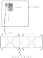
図7は、実施の形態1におけるサブ画素補間処理で求める画素位置を説明するための図である。図7の例において、被検査画像10に対して、参照画像12をサブ画素単位でずらした場合、被検査画像10の3×3の画素の中心画素と比較される参照画像12の補間画素Gi,jは、参照画像12の画素Gi−1,j−1、画素Gi+1,j−1、画素Gi−1,j+1、画素Gi+1,j+1によって囲まれた位置になる。よって、参照画像12の補間画素Gi,jの画素値は、その周囲の参照画像12の画素の画素値を用いて補間されることになる。これにより、被検査画像10の画素に合わせた位置で被検査画像10と参照画像12とを比較することができる。ここで、「その周囲の参照画像12の画素」として、例えば、2×2=4画素の他、さらにその1回り外側の画素も含む、4×4=16画素を用いると良い。ここでは、1次元の補間に分解して、左2つ右2つの4画素を使った補間をした後、上2つ下2つの補間を続けて行なう。
FIG. 7 is a diagram for explaining the pixel position obtained by the sub-pixel interpolation process in the first embodiment. In the example of FIG. 7, when the
図8は、実施の形態1におけるサブ画素補間処理の仕方を説明するための図である。図8の例では、1次元方向(x方向)へ画像をシフトする場合の補間処理を示している。図8(a)において参照画像をシフトした場合に、被検査画像の各画素の位置での画素値gxを補間により求める場合、シフト方向の両側に隣接する2画素ずつ計4画素の周辺画素(−1,0,1,2)の画素値(g−1,g0,g1,g2)を用いて補間する。かかる場合、対象画素は、周辺画素(0)と周辺画素(1)との間にあって、周辺画素(0)からシフト量xだけずらした位置になる場合を想定している。かかる場合の対象画素の画素値gxは、図8(b)に示すように、4つの周辺画素の画素値を用いた線形和で定義できる。具体的には、4つの周辺画素の画素値にそれぞれ重み付け係数q−1〜q2を乗じた値の和を示す式(3)(補間フィルタ関数)で定義できる。
(3) gx=q−1・g−1+q0・g0+q1・g1+q2・g2
FIG. 8 is a diagram for explaining a method of sub-pixel interpolation processing in the first embodiment. In the example of FIG. 8, the interpolation processing in the case of shifting the image in the one-dimensional direction (x direction) is shown. When the reference image is shifted in FIG. 8A and the pixel value gx at the position of each pixel of the image to be inspected is obtained by interpolation, two adjacent pixels on both sides in the shift direction are used to obtain a total of four peripheral pixels (4 pixels in total). Interpolation is performed using the pixel values (g- 1 , g0, g1, g2 ) of -1, 0 , 1 , 2). In such a case, it is assumed that the target pixel is located between the peripheral pixel (0) and the peripheral pixel (1) and is shifted from the peripheral pixel (0) by the shift amount x. As shown in FIG. 8B, the pixel value gx of the target pixel in such a case can be defined by a linear sum using the pixel values of the four peripheral pixels. Specifically, it can be defined by the equation (3) (interpolation filter function) showing the sum of the values obtained by multiplying the pixel values of the four peripheral pixels by the weighting coefficients q -1 to q 2.
(3) gx = q -1・ g -1 + q 0・ g 0 + q 1・ g 1 + q 2・ g 2
かかる場合、重み付け係数q−1〜q2は、シフト量xに依存した関数で定義され、図8(b)に示すように、重み付け係数q−1〜q2の和は1になり、重み付け係数q−1〜q2の二乗和はシフト量xに依存した関数f(x)になるように定義される。重み付け係数q−1〜q2は、シフト量xの1次関数であっても良いし、2次以降の高次関数であっても良い。例えば3次関数を用いる。 In such a case, the weighting coefficients q -1 to q 2 are defined by a function depending on the shift amount x, and as shown in FIG. 8 (b), the sum of the weighting coefficients q -1 to q 2 becomes 1, and the weighting is performed. The sum of squares of the coefficients q -1 to q 2 is defined to be a function f (x) depending on the shift amount x. The weighting coefficients q -1 to q 2 may be a linear function of the shift amount x, or may be a higher-order function of the second or higher order. For example, a cubic function is used.
2次元方向(x方向およびy方向)へ画像をシフトする場合には、上記の方法で1次元方向(x方向)に画像をシフトした後、さらに同様の方法で1次元方向(y方向)に画像をシフトすればよい。 When shifting the image in the two-dimensional direction (x direction and y direction), after shifting the image in the one-dimensional direction (x direction) by the above method, the same method is used to shift the image in the one-dimensional direction (y direction). Just shift the image.
次に、SSD値算出部62(差分二乗和演算部)は、ずらし量毎に、被検査画像の各画素値と補間処理された参照画像の対応する画素値との差分二乗和(SSD)を演算する。 Next, the SSD value calculation unit 62 (difference squared sum calculation unit) calculates the difference squared sum (SSD) of each pixel value of the image to be inspected and the corresponding pixel value of the interpolated reference image for each shift amount. Calculate.
次に、最適化処理部64は、差分二乗和(SSD)が最小となる画像シフト量(ずらし量)を演算する。そのために、最適化処理部64は、画像シフト量を可変にずらして、その都度、設定した画像シフト量をサブ画素補間処理部60に出力する。そして、サブ画素補間処理部60は、上述したように設定された画像シフト量で参照画像を補間し、SSD値算出部62が差分二乗和(SSD)を演算し、演算結果を最適化処理部64に出力する。以上のようにして、最適化処理部64は、差分二乗和(SSD)が最小となる画像シフト量(ずらし量)を求める。以上の繰り返し演算によって得られた、差分二乗和(SSD)が最小となる画像シフト量(ずらし量)は、サブ画素補間処理部66に出力される。
Next, the
以上のように、実施の形態1では、まず、スムージング処理によって、実質的にショットノイズを含むノイズを消去した後で、画像シフト量(ずらし量)を求めるので、ノイズの影響を受けていない位置合わせ用の画像シフト量(ずらし量)を得ることができる。しかし、ここでは、ノイズを消去するほどの強めのスムージング処理を行っているので各画素値が大きく変更されており、画像が所謂ぼけた状態になっている。よって、そのまま画像比較を行っても高精度な結果を得ることは困難である。そこで、得られた画像シフト量(ずらし量)を使ってスムージング処理前の両画像の位置合わせを行っていく。 As described above, in the first embodiment, first, the noise including shot noise is substantially eliminated by the smoothing process, and then the image shift amount (shift amount) is obtained, so that the position is not affected by the noise. The image shift amount (shift amount) for matching can be obtained. However, here, since a strong smoothing process is performed to eliminate noise, each pixel value is significantly changed, and the image is in a so-called blurred state. Therefore, it is difficult to obtain highly accurate results even if the images are compared as they are. Therefore, the obtained image shift amount (shift amount) is used to align both images before the smoothing process.
サブ画素補間処理部66(第2のサブ画素補間処理部)は、記憶装置50からスムージング処理を行っていない参照画像となるマスクダイ画像を読み出し、スムージング処理を行っていない参照画像の少なくとも1つの画素値を用いて差分二乗和が最小となる画像シフト量(ずらし量)にて補間処理することにより被検査画像の各画素の位置に対応する当該参照画像の画素値を演算する。これにより、ノイズの影響を受けていない本来の図形パターン同士による位置合わせを行い得る高精度な画像シフト量(ずらし量)で参照画像を補間処理できる。補間処理の仕方は、上述した内容と同様である。画像シフト量(ずらし量)にて補間処理された参照画像の補間画像は記憶装置68に格納される。
The sub-pixel interpolation processing unit 66 (second sub-pixel interpolation processing unit) reads out a mask die image that is a reference image that has not been smoothed from the
ここで、強めのスムージング処理を行っていない参照画像の画素値にはショットノイズの成分が含まれている。そして、補間処理における重み付け係数q−1〜q2の二乗和で定義される、シフト量xに依存した関数f(x)の平行根が、ショットノイズのレベルの比率を示している。言い換えれば、シフト量xに依存した関数f(x)の平行根が小さくなるほど、ショットノイズのレベルが小さくなる。よって、ショットノイズのレベルは、シフト量(ずらし量)xに依存して変動することになる。そのため、サブ画素補間処理部66による補間処理においても、その結果得られる画素値には、シフト量(ずらし量)xに依存したショットノイズのレベルの変動分が含まれていることになる。 Here, the pixel value of the reference image that has not been subjected to the strong smoothing process contains a shot noise component. The parallel roots of the function f (x), which is defined by the sum of squares of the weighting coefficients q -1 to q 2 in the interpolation process and depends on the shift amount x, indicate the ratio of the shot noise levels. In other words, the smaller the parallel roots of the function f (x) that depends on the shift amount x, the smaller the shot noise level. Therefore, the shot noise level fluctuates depending on the shift amount (shift amount) x. Therefore, even in the interpolation processing by the sub-pixel interpolation processing unit 66, the pixel value obtained as a result includes the fluctuation of the shot noise level depending on the shift amount (shift amount) x.
図9は、実施の形態1におけるサブ画素シフト量とノイズレベルとの関係の一例を示している。図9(a)では、3次元でノイズレベルの比率を示している。図9(b)では、2次元でノイズレベルの比率を示している。いずれにおいても、サブ画素単位でのシフト量xがゼロの場合、補間処理による平均化効果が得られないのでノイズレベルの比率は最大値である1となる。これに対して、サブ画素単位でのシフト量xが1/2画素に向かって大きくなるにつれて、ノイズレベルの比率が小さくなり、シフト量xが1/2画素において最小値を得ることがわかる。周囲の画素から共に均等な距離で平均化効果が最大を示す。シミュレーションの結果、x,y方向にそれぞれ1/2画素ずつシフトさせた場合の補間値において、ノイズレベルの比率が最小値の例えば0.64(64%)まで低減することがわかっている。 FIG. 9 shows an example of the relationship between the sub-pixel shift amount and the noise level in the first embodiment. FIG. 9A shows the ratio of noise levels in three dimensions. FIG. 9B shows the ratio of noise levels in two dimensions. In either case, when the shift amount x in the sub-pixel unit is zero, the averaging effect by the interpolation processing cannot be obtained, so the noise level ratio is 1, which is the maximum value. On the other hand, as the shift amount x in the sub-pixel unit increases toward 1/2 pixel, the noise level ratio decreases, and it can be seen that the shift amount x obtains the minimum value in 1/2 pixel. The averaging effect is maximized at an equal distance from the surrounding pixels. As a result of the simulation, it is known that the noise level ratio is reduced to the minimum value, for example, 0.64 (64%), in the interpolated value when the interpolation value is shifted by 1/2 pixel in each of the x and y directions.
図10は、実施の形態1における参照画像をシフトさせて補間処理した場合の補間画像の一例を示す図である。図10(a)では、シフト量がゼロの場合の画像の一例を示している。これに対して、図10(b)では、x,y方向にそれぞれ1/2画素分ずつシフトさせた場合での画素値を補間した補間画像の一例を示している。図10(b)に示す画像では、補間により画素値が平均化されるためパターンのエッジがぼやけてしまうが、同時にショットノイズのレベルについては、平均化により最小になっている。 FIG. 10 is a diagram showing an example of an interpolated image when the reference image in the first embodiment is shifted and interpolated. FIG. 10A shows an example of an image when the shift amount is zero. On the other hand, FIG. 10B shows an example of an interpolated image in which the pixel values are interpolated when the pixels are shifted by 1/2 pixel in the x and y directions, respectively. In the image shown in FIG. 10B, the pixel values are averaged by interpolation, so that the edges of the pattern are blurred, but at the same time, the shot noise level is minimized by averaging.
以上のように、サブ画素補間処理部66により補間処理された参照画像の補間画像の各画素値には、シフト量(ずらし量)xに依存したショットノイズのレベルの変動分が含まれている。よって、補間処理を行っていない被検査画像と比較する場合、補間画像(参照画像)と被検査画像との間に、かかるシフト量(ずらし量)xに依存したショットノイズのレベル変動分のずれが生じている。言い換えれば、同じノイズレベル条件での比較が困難な状況になっている。そこで、実施の形態1では、かかるシフト量(ずらし量)xに依存したノイズレベルの変化を打ち消すフィルタ処理を行う。 As described above, each pixel value of the interpolated image of the reference image interpolated by the sub-pixel interpolation processing unit 66 includes a variation in the shot noise level depending on the shift amount (shift amount) x. .. Therefore, when comparing with the image to be inspected that has not been interpolated, the deviation of the shot noise level fluctuation depending on the shift amount (shift amount) x between the interpolated image (reference image) and the image to be inspected. Has occurred. In other words, it is difficult to make comparisons under the same noise level conditions. Therefore, in the first embodiment, a filter process is performed to cancel the change in the noise level depending on the shift amount (shift amount) x.
補償フィルタ処理部68(フィルタ処理部)は、差分二乗和が最小となるシフト量(ずらし量)にて補間処理された参照画像に対してシフト量(ずらし量)に依存するノイズの影響を抑制するフィルタ関数を用いてフィルタ処理する。 The compensation filter processing unit 68 (filter processing unit) suppresses the influence of noise depending on the shift amount (shift amount) on the reference image interpolated by the shift amount (shift amount) that minimizes the sum of squared differences. Filter using the filter function to be used.
図11は、実施の形態1における補償フィルタ処理の仕方を説明するための図である。図11の例では、x方向のフィルタ処理を示しているが、y方向に関しても同様である。図11(a)において、補間処理後の補間画像(参照画像)の各画素の画素値について、シフト量(ずらし量)xに依存したノイズレベルの変化が打ち消された画素値g’を求める場合、補間処理されている当該画素とシフト方向の両側に隣接する1画素ずつ計3画素(−1,0,1)の画素値(g−1,g0,g1)を用いて補間する。かかる場合、対象画素は、画素(0)にある場合を想定している。上述したように、サブ画素補間処理部66による補間処理において、ショットノイズのノイズレベルの比率は、シフト量xに依存した関数f(x)の平行根で示される。よって、ノイズレベルが最小値となるシフト量(ずらし量)x’(参照画像のみをシフトさせる場合にはx’は0.5画素)における関数f(x’)の平行根が、ノイズレベルが最小となる場合を示していることになる。そこで、かかる場合の対象画素の画素値g’は、図11(b)に示すように、3つの画素の画素値を用いた線形和で定義できる。具体的には、周辺画素の画素値にそれぞれ重み付け係数c1を乗じた2つの値と当該の画素値に重み付け係数c0を乗じた値の和を示す式(3)(補償フィルタ関数)で定義できる。
(3) g’=c1・g−1+c0・g0+c1・g1
FIG. 11 is a diagram for explaining a method of compensation filter processing in the first embodiment. In the example of FIG. 11, the filter processing in the x direction is shown, but the same applies to the y direction. In FIG. 11A, for the pixel value of each pixel of the interpolated image (reference image) after the interpolation processing, the pixel value g'in which the change in the noise level depending on the shift amount (shift amount) x is canceled out is obtained. , Interpolation is performed using the pixel values (g-1 , g 0 , g 1 ) of a total of 3 pixels (-1, 0, 1), one pixel adjacent to each of the pixel being interpolated and one pixel adjacent to each side in the shift direction. In such a case, it is assumed that the target pixel is in the pixel (0). As described above, in the interpolation processing by the sub-pixel interpolation processing unit 66, the ratio of the noise level of the shot noise is indicated by the parallel roots of the function f (x) depending on the shift amount x. Therefore, the noise level is the parallel root of the function f (x') in the shift amount (shift amount) x'(x'is 0.5 pixel when only the reference image is shifted) at which the noise level becomes the minimum value. It shows the case where it becomes the minimum. Therefore, the pixel value g'of the target pixel in such a case can be defined by a linear sum using the pixel values of the three pixels, as shown in FIG. 11B. Specifically, it is an equation (3) (compensation filter function) showing the sum of two values obtained by multiplying the pixel values of peripheral pixels by the weighting coefficient c 1 and the value obtained by multiplying the pixel value by the weighting coefficient c 0. Can be defined.
(3) g'= c 1 · g -1 + c 0 · g 0 + c 1 · g 1
かかる場合、図11(b)に示すように、重み付け係数c1,c0,c1の和は1になり、重み付け係数c1,c0,c1の二乗和は、ノイズレベルが最小となる関数f(x’)をシフト量xに依存した関数f(x)で割った値になるように定義される。重み付け係数c0,c1は、シフト量xの1次関数であっても良いし、2次以降の高次関数であっても良い。なお、図11(b)からc0,c1は容易に解くことができる。
In this case, as shown in FIG. 11 (b), the sum of the weighting factors c 1,
以上、x方向のフィルタ処理について説明したが、y方向に関しても同様の処理を行なう。x方向のフィルタ処理の結果得られた画像に対して、同様の方法でy方向に関してもフィルタ処理を行なう。補償フィルタ係数については、xの代わりにy方向のシフト量(ずらし量)yを用いて決定する。2次元のデータにフィルタ処理を行う際は、例えば最初にx方向に1次元のフィルタ処理を行い、その結果に対してさらにy方向に1次元のフィルタ処理を行う。 The filter processing in the x direction has been described above, but the same processing is performed in the y direction as well. The image obtained as a result of the filter processing in the x direction is filtered in the y direction in the same manner. The compensation filter coefficient is determined by using the shift amount (shift amount) y in the y direction instead of x. When performing a filter process on two-dimensional data, for example, a one-dimensional filter process is first performed in the x direction, and then a one-dimensional filter process is further performed in the y direction for the result.
サブ画素補間処理部66により補間処理された際に、シフト量xに依存した関数f(x)の影響を受けているので、補償フィルタ処理では、重み付け係数c1,c0,c1の二乗和として、ノイズレベルが最小となる関数f(x’)を用い、さらに、関数f(x’)に1/f(x)を乗じることで、既に補間処理された際に生じているシフト量xに依存したノイズレベルの変化を排除する。これにより、補償フィルタ処理後の補間画像は、シフト量xに依存したノイズレベルの変化が打ち消された条件での画素値g’にできる。 When the interpolation processing is performed by the subpixel interpolation processing unit 66, it is affected by the function f (x) depending on the shift amount x. Therefore, in the compensation filter processing, the weighting coefficients c 1 , c 0 , and c 1 are squared. As the sum, the function f (x') that minimizes the noise level is used, and by multiplying the function f (x') by 1 / f (x), the shift amount that has already occurred when interpolation processing is performed. Eliminate x-dependent changes in noise level. As a result, the interpolated image after the compensation filter processing can be set to the pixel value g'under the condition that the change in the noise level depending on the shift amount x is canceled.
図12は、実施の形態1におけるシフト量の異なる補間画像と補償フィルタ補間画像との一例を示す図である。図12(a)では、シフト量(ずらし量)x=0に補間された補間画像の一例を示す。図12(b)では、シフト量(ずらし量)x=1/2画素に補間された補間画像の一例を示す。図12(a)に示す補間画像と図12(b)に示す補間画像とでは、ノイズレベルが大きく異なる。これに対して、図12(c)では、図12(a)に示す補間画像に対して補償フィルタ処理を実施した補償フィルタ補間画像を示す。また、図12(d)では、図12(b)に示す補間画像に対して補償フィルタ処理を実施した補償フィルタ補間画像を示す。図12(c)に示す補償フィルタ補間画像と図12(d)に示す補償フィルタ補間画像とでは、肉眼では見分けにくいが、ノイズレベルが同じになるように揃えられている。よって、補償フィルタ関数により処理によって、シフト量xに依存したノイズレベルの変化が打ち消されている。補償フィルタ処理により得られた補償フィルタ補間画像は、記憶装置69に格納される。
FIG. 12 is a diagram showing an example of an interpolated image having a different shift amount and a compensation filter interpolated image according to the first embodiment. FIG. 12A shows an example of an interpolated image interpolated to a shift amount (shift amount) x = 0. FIG. 12B shows an example of an interpolated image interpolated to a shift amount (shift amount) x = 1/2 pixel. The noise level is significantly different between the interpolated image shown in FIG. 12 (a) and the interpolated image shown in FIG. 12 (b). On the other hand, FIG. 12 (c) shows a compensation filter interpolated image obtained by performing compensation filter processing on the interpolated image shown in FIG. 12 (a). Further, FIG. 12 (d) shows a compensation filter interpolated image obtained by performing compensation filter processing on the interpolated image shown in FIG. 12 (b). The compensation filter interpolated image shown in FIG. 12 (c) and the compensation filter interpolated image shown in FIG. 12 (d) are arranged so that the noise levels are the same, although they are difficult to distinguish with the naked eye. Therefore, the change in the noise level depending on the shift amount x is canceled by the processing by the compensation filter function. The compensation filter interpolated image obtained by the compensation filter processing is stored in the
一方、被検査画像について、ノイズを消去するほどの強めのスムージング処理を行った画像では、参照画像と同様、各画素値が大きく変更されており、画像が所謂ぼけた状態になっている。よって、そのまま画像比較を行っても高精度な結果を得ることは困難である。また、スムージング処理を行う前の画像では、補間処理を行っていないのでシフト量xに依存したノイズレベルの変化は生じていない。他方、参照画像では、補償フィルタにより、シフト量xに依存したノイズレベルの変化を打ち消したものの、x,y方向に3画素によるフィルタ処理によるスムージング効果は働いている。そこで、被検査画像についても、補償フィルタ処理と同程度のスムージング効果が得られるスムージング処理を行って条件を同程度に近づける。 On the other hand, in the image to be inspected, which has been subjected to a strong smoothing process to eliminate noise, each pixel value is significantly changed as in the reference image, and the image is in a so-called blurred state. Therefore, it is difficult to obtain highly accurate results even if the images are compared as they are. Further, in the image before the smoothing process, since the interpolation process is not performed, the noise level does not change depending on the shift amount x. On the other hand, in the reference image, although the change in the noise level depending on the shift amount x is canceled by the compensation filter, the smoothing effect by the filter processing by the three pixels in the x and y directions is working. Therefore, for the image to be inspected, the smoothing process that can obtain the same smoothing effect as the compensation filter process is performed to bring the conditions closer to the same level.
スムージング処理部70は、記憶装置20からスムージング処理を行っていない被検査画像となるマスクダイ画像を読み出し、被検査画像となるマスクダイ画像内の図形パターンに対してパターン端部を若干なめらかにする弱めのスムージング処理を行う。スムージング処理用のフィルタとしては、補償フィルタ処理部69と同様の3画素によるフィルタをx、y方向に掛けるものを用いるが、フィルタの係数はずらし量によって変化させず、x=y=0に対して求めた係数を常に用いる。これにより、参照画像と被検査画像に同程度の強さのスムージング効果が効いた状態で後段の比較処理部72へと入力される。
The smoothing
以上のように、実施の形態1によれば、スムージング処理により、ショットノイズが存在しても、被検査画像と参照画像との高精度な位置合わせができる。さらに、補償フィルタ処理により画像シフト量に依存したノイズレベルの変動分を消去しているので、位置合わせの結果得られるシフト量に関係なくノイズレベルを同じ状態に合わせることができる。さらに被検査画像に対してもこれと同等のスムージング効果をもつフィルタを掛けることで、被検査画像のノイズレベルも同様の状態に合わせることができる。かかる状態で、被検査画像と参照画像とを比較する。 As described above, according to the first embodiment, the smoothing process enables highly accurate alignment between the image to be inspected and the reference image even in the presence of shot noise. Further, since the noise level fluctuation depending on the image shift amount is eliminated by the compensation filter processing, the noise level can be adjusted to the same state regardless of the shift amount obtained as a result of the alignment. Further, by applying a filter having the same smoothing effect to the image to be inspected, the noise level of the image to be inspected can be adjusted to the same state. In this state, the image to be inspected and the reference image are compared.
比較処理部72(比較部)は、被検査画像と上述したスムージング処理が成された状態で差分二乗和が最小となるずらし量にて補間処理された参照画像とを比較する。ここでは、被検査画像が、さらに補償フィルタ処理もなされた参照画像(補償フィルタ補間画像)と比較される。具体的には、被検査画像と参照画像とを、画素毎に比較する。所定の判定閾値を用いて所定の判定条件に従って画素毎に両者を比較し、例えば形状欠陥といった欠陥の有無を判定する。例えば、画素毎の階調値差が判定閾値Thよりも大きければ欠陥候補と判定する。そして、比較結果が出力される。比較結果は、記憶装置109、モニタ117、若しくはメモリ118に、或いはプリンタ119より出力されればよい。
The comparison processing unit 72 (comparison unit) compares the image to be inspected with the reference image interpolated with a shift amount that minimizes the sum of squared differences in the state where the smoothing processing described above is performed. Here, the image to be inspected is compared with a reference image (compensation filter interpolated image) that has also been subjected to compensation filtering processing. Specifically, the image to be inspected and the reference image are compared for each pixel. Using a predetermined determination threshold value, the two are compared for each pixel according to a predetermined determination condition, and the presence or absence of a defect such as a shape defect is determined. For example, if the gradation value difference for each pixel is larger than the determination threshold value Th, it is determined as a defect candidate. Then, the comparison result is output. The comparison result may be output to the
或いは、比較処理部72(比較部)は、被検査画像と参照画像(補償フィルタ補間画像)とからそれぞれ画像内の図形パターンの輪郭線を生成する。そして、マッチングする図形パターンの輪郭線同士のずれを比較して良い。例えば、輪郭線同士のずれが判定閾値Th’よりも大きければ欠陥候補と判定する。そして、比較結果が出力される。比較結果は、記憶装置109、モニタ117、若しくはメモリ118に、或いはプリンタ119より出力されればよい。
Alternatively, the comparison processing unit 72 (comparison unit) generates contour lines of graphic patterns in the image from the image to be inspected and the reference image (compensation filter interpolated image), respectively. Then, the deviations between the contour lines of the matching graphic patterns may be compared. For example, if the deviation between the contour lines is larger than the determination threshold value Th', it is determined as a defect candidate. Then, the comparison result is output. The comparison result may be output to the
なお、上述した例では、ダイーダイ検査を行う場合について説明したが、ダイーデータベース検査を行う場合にも同様に適用できる。かかる場合、参照画像作成回路112は、基板101にパターンを形成する基になった設計データ、或いは基板101に形成されたパターンの露光イメージデータに定義された設計パターンデータに基づいて、マスクダイ毎に、参照画像を作成する。具体的には、以下のように動作する。まず、記憶装置109から制御計算機110を通して設計パターンデータを読み出し、読み出された設計パターンデータに定義された各図形パターンを2値ないしは多値のイメージデータに変換する。
In the above-mentioned example, the case of performing the Die-Die inspection has been described, but the same can be applied to the case of performing the Die database inspection. In such a case, the reference
ここで、設計パターンデータに定義される図形は、例えば長方形や三角形を基本図形としたもので、例えば、図形の基準位置における座標(x、y)、辺の長さ、長方形や三角形等の図形種を区別する識別子となる図形コードといった情報で各パターン図形の形、大きさ、位置等を定義した図形データが格納されている。 Here, the figure defined in the design pattern data is, for example, a figure having a rectangle or a triangle as a basic figure, for example, a figure such as a coordinate (x, y), a side length, a rectangle or a triangle at a reference position of the figure. Graphical data that defines the shape, size, position, etc. of each pattern graphic is stored with information such as a graphic code that serves as an identifier for distinguishing species.
かかる図形データとなる設計パターンデータが参照画像作成回路112に入力されると図形ごとのデータにまで展開し、その図形データの図形形状を示す図形コード、図形寸法などを解釈する。そして、所定の量子化寸法のグリッドを単位とするマス目内に配置されるパターンとして2値ないしは多値の設計パターン画像データに展開し、出力する。言い換えれば、設計データを読み込み、検査領域を所定の寸法を単位とするマス目として仮想分割してできたマス目毎に設計パターンにおける図形が占める占有率を演算し、nビットの占有率データを出力する。例えば、1つのマス目を1画素として設定すると好適である。そして、1画素に1/28(=1/256)の分解能を持たせるとすると、画素内に配置されている図形の領域分だけ1/256の小領域を割り付けて画素内の占有率を演算する。そして、8ビットの占有率データとして参照回路112に出力する。かかるマス目(検査画素)は、測定データの画素に合わせればよい。
When the design pattern data to be the graphic data is input to the reference
次に、参照画像作成回路112は、図形のイメージデータである設計パターンの設計画像データに適切なフィルタ処理を施す。測定画像としての光学画像データは、光学系によってフィルタが作用した状態、言い換えれば連続変化するアナログ状態にあるため、画像強度(濃淡値)がデジタル値の設計側のイメージデータである設計画像データにもフィルタ処理を施すことにより、測定データに合わせることができる。作成された参照画像の画像データは比較回路108に出力され、メモリ50に格納される。比較回路108内での処理内容は、上述したダイーダイ検査を行う場合と同様で構わない。設計データから作成される設計画像には、そもそもショットノイズは含まれていない。しかし、位置合わせの際の補間処理により、ショットノイズの代わりにシフト量xに依存した画像のボケが生じ得る。よって、同様に処理を行うことで、ダイーダイ検査を行う場合と同様の効果を得ることができる。
Next, the reference
以上のように、実施の形態1によれば、ノイズの影響を低減した画像同士の位置合わせができる。そのため、高精度なパターン検査ができる。 As described above, according to the first embodiment, the images can be aligned with each other with the influence of noise reduced. Therefore, highly accurate pattern inspection can be performed.
実施の形態2.
実施の形態1では、ノイズ成分自体を消去してから位置合わせを行う構成について説明したが、実施の形態2では、画像シフト量(ずらし量)に依存したノイズレベルの変動分を消去した上で位置合わせを行う構成について説明する。実施の形態2における検査装置100の構成は図1と同様である。また、以下、特に説明する点以外の内容は、実施の形態1と同様で構わない。
In the first embodiment, the configuration in which the noise component itself is erased and then the alignment is performed has been described, but in the second embodiment, the fluctuation amount of the noise level depending on the image shift amount (shift amount) is erased. A configuration for performing alignment will be described. The configuration of the
図13は、実施の形態2における比較回路内の構成を示す内部構成図の一例である。図13において、比較回路108内には、磁気ディスク装置等の記憶装置50,52,74、位置合わせ部58、及び比較処理部72が配置される。位置合わせ部58内には、内部構成として、サブ画素補間処理部60、SSD(Sum of Squared Difference)値算出部62、最適化処理部64、補償フィルタ処理部68、及びスムージング処理部70が配置される。位置合わせ部58(サブ画素補間処理部60、SSD値算出部62、最適化処理部64、補償フィルタ処理部68、及びスムージング処理部70)、及び比較処理部72といった各「〜部」は、処理回路を含み、その処理回路には、電気回路、コンピュータ、プロセッサ、回路基板、量子回路、或いは、半導体装置等が含まれる。また、各「〜部」は、共通する処理回路(同じ処理回路)を用いてもよい。或いは、異なる処理回路(別々の処理回路)を用いても良い。位置合わせ部58(サブ画素補間処理部60、SSD値算出部62、最適化処理部64、補償フィルタ処理部68、及びスムージング処理部70)、及び比較処理部72内に必要な入力データ或いは演算された結果はその都度図示しないメモリに記憶される。実施の形態1では、位置合わせ部58内で位置合わせ用の画像シフト量の最適化を行った後で、元の画像に補償フィルタ処理を行ったが、実施の形態2では、図13に示すように、位置合わせ部58内で位置合わせ用の画像シフト量の最適化を行うループ内で画像に補償フィルタ処理を行う。
FIG. 13 is an example of an internal configuration diagram showing a configuration in the comparison circuit according to the second embodiment. In FIG. 13,
比較回路108に転送された測定データのうち、被検査画像となるマスクダイ33の画像(マスクダイ画像)は記憶装置52(第1の記憶装置)に格納(記憶)される。被検査画像に対応する参照画像となるマスクダイ33の画像(マスクダイ画像)は記憶装置50(第2の記憶装置)に格納(記憶)される。
Of the measurement data transferred to the
サブ画素補間処理部60(サブ画素補間処理部)は、被検査画像に対応する参照画像を用いて、被検査画像と参照画像とを相対的にサブ画素単位で可変にずらしながら、当該参照画像の少なくとも1つの画素値を用いて補間処理することにより被検査画像の各画素の位置に対応する当該参照画像の画素値を演算する。実施の形態2では、上述したスムージング処理が実施されていない被検査画像を固定した状態で、上述したスムージング処理が実施されていない参照画像となるマスクダイ画像をサブ画素単位でずらしていく場合について説明する。1画素が例えば256階調で定義される場合、例えば、x,y方向に1/16画素ずつ、或いは1/8画素ずつシフトさせると好適である。補間処理の仕方は、図8(a)で説明したように、参照画像をシフトした場合に、被検査画像の各画素の位置での画素値gxを補間により求める場合、シフト方向の両側に隣接する2画素ずつ計4画素の周辺画素(−1,0,1,2)の画素値(g−1,g0,g1,g2)を用いて補間する。かかる場合、対象画素は、周辺画素(0)と周辺画素(1)との間にあって、周辺画素(0)からシフト量xだけずらした位置になる場合を想定している。かかる場合の対象画素の画素値gxは、図8(b)に示すように、4つの周辺画素の画素値を用いた線形和で定義できる。具体的には、4つの周辺画素の画素値にそれぞれ重み付け係数q−1〜q2を乗じた値の和を示す上述した式(3)(補間フィルタ関数)で定義できる。 The sub-pixel interpolation processing unit 60 (sub-pixel interpolation processing unit) uses the reference image corresponding to the inspected image, and while variably shifting the inspected image and the reference image in sub-pixel units, the reference image. By performing interpolation processing using at least one pixel value of, the pixel value of the reference image corresponding to the position of each pixel of the image to be inspected is calculated. In the second embodiment, a case is described in which the mask die image, which is the reference image to which the above-mentioned smoothing process is not performed, is shifted in units of sub-pixels in a state where the image to be inspected to which the above-mentioned smoothing process is not performed is fixed. do. When one pixel is defined by, for example, 256 gradations, it is preferable to shift by 1/16 pixel or 1/8 pixel in the x and y directions, for example. As described in FIG. 8A, when the reference image is shifted and the pixel value gx at the position of each pixel of the image to be inspected is obtained by interpolation, the method of interpolation processing is adjacent to both sides in the shift direction. Interpolation is performed using the pixel values (g-1 , g 0 , g 1 , g 2 ) of the peripheral pixels (-1, 0, 1, 2) of a total of 4 pixels for each of 2 pixels. In such a case, it is assumed that the target pixel is located between the peripheral pixel (0) and the peripheral pixel (1) and is shifted from the peripheral pixel (0) by the shift amount x. As shown in FIG. 8B, the pixel value gx of the target pixel in such a case can be defined by a linear sum using the pixel values of the four peripheral pixels. Specifically, it can be defined by the above-mentioned equation (3) (interpolation filter function) showing the sum of the values obtained by multiplying the pixel values of the four peripheral pixels by the weighting coefficients q -1 to q 2, respectively.
かかる場合、重み付け係数q−1〜q2は、シフト量xに依存した関数で定義され、図8(b)に示すように、重み付け係数q−1〜q2の和は1になり、重み付け係数q−1〜q2の二乗和はシフト量xに依存した関数f(x)になるように定義される。重み付け係数q−1〜q2は、シフト量xの1次関数であっても良いし、2次以降の高次関数であっても良い。 In such a case, the weighting coefficients q -1 to q 2 are defined by a function depending on the shift amount x, and as shown in FIG. 8 (b), the sum of the weighting coefficients q -1 to q 2 becomes 1, and the weighting is performed. The sum of squares of the coefficients q -1 to q 2 is defined to be a function f (x) depending on the shift amount x. The weighting coefficients q -1 to q 2 may be a linear function of the shift amount x, or may be a higher-order function of the second or higher order.
さらにy方向へ画像をシフトする場合、シフト量yについて同様に補間すればよい。 Further, when the image is shifted in the y direction, the shift amount y may be similarly interpolated.
以上のように、サブ画素補間処理部60により補間処理された参照画像の補間画像の各画素値には、シフト量(ずらし量)xに依存したショットノイズのレベルの変動分が含まれている。よって、補間処理を行っていない被検査画像と比較する場合、補間画像(参照画像)と被検査画像との間に、かかるシフト量(ずらし量)xに依存したショットノイズのレベル変動分のずれが生じている。言い換えれば、同じノイズレベル条件での比較が困難な状況になっている。そこで、実施の形態2では、かかるシフト量(ずらし量)xに依存したノイズレベルの変化を打ち消すフィルタ処理を行う。
As described above, each pixel value of the interpolated image of the reference image interpolated by the sub-pixel
補償フィルタ処理部68(フィルタ処理部)は、画像シフト量(ずらし量)毎に、補間処理された当該参照画像(補間画像)の画素値に対して画像シフト量(ずらし量)に依存するノイズの影響を抑制するフィルタ関数を用いてフィルタ処理する。具体的には、図11(a)にて説明したように、補間処理後の補間画像(参照画像)の各画素の画素値について、シフト量(ずらし量)xに依存したノイズレベルの変化が打ち消された画素値g’を求める場合、補間処理されている当該画素とシフト方向の両側に隣接する1画素ずつ計3画素(−1,0,1)の画素値(g−1,g0,g1)を用いて補間する。かかる場合、対象画素は、画素(0)にある場合を想定している。かかる場合の対象画素の画素値g’は、図11(b)に示すように、3つの画素の画素値を用いた線形和で定義できる。具体的には、周辺画素の画素値にそれぞれ重み付け係数c1を乗じた2つの値と当該の画素値に重み付け係数c0を乗じた値の和を示す、上述した式(3)(補償フィルタ関数)で定義できる。 The compensation filter processing unit 68 (filter processing unit) is a noise that depends on the image shift amount (shift amount) with respect to the pixel value of the interpolated reference image (interpolated image) for each image shift amount (shift amount). Filter using a filter function that suppresses the influence of. Specifically, as described with reference to FIG. 11A, the change in the noise level depending on the shift amount (shift amount) x with respect to the pixel value of each pixel of the interpolated image (reference image) after the interpolation processing is performed. When obtaining the canceled pixel value g', the pixel value (g-1 , g 0 ) of a total of 3 pixels (-1, 0, 1) is obtained, one pixel each adjacent to the interpolated pixel and one pixel adjacent to each side in the shift direction. , G 1 ) is used for interpolation. In such a case, it is assumed that the target pixel is in the pixel (0). As shown in FIG. 11B, the pixel value g'of the target pixel in such a case can be defined by a linear sum using the pixel values of the three pixels. Specifically, the above-mentioned equation (3) (compensation filter) showing the sum of two values obtained by multiplying the pixel values of the peripheral pixels by the weighting coefficient c 1 and the value obtained by multiplying the pixel values by the weighting coefficient c 0. Can be defined by function).
かかる場合、図11(b)に示すように、重み付け係数c1,c0,c1の和は1になり、重み付け係数c1,c0,c1の二乗和は、ノイズレベルが最小となる関数f(x’)をシフト量xに依存した関数f(x)で割った値になるように定義される。重み付け係数c0,c1は、シフト量xの1次関数であっても良いし、2次以降の高次関数であっても良い。上述したように、ノイズレベルが最小となる関数f(x’)に1/f(x)を乗じることで、既に補間処理された際に生じているシフト量xに依存したノイズレベルの変化を排除する。これにより、補償フィルタ処理後の補間画像は、シフト量xに依存したノイズレベルの変化が打ち消された条件での画素値g’にできる。
In this case, as shown in FIG. 11 (b), the sum of the weighting factors c 1,
シフト量yについて同様にフィルタ処理する。2次元のデータにフィルタ処理を行う際は、例えば最初にx方向に1次元のフィルタ処理を行い、その結果に対してさらにy方向に1次元のフィルタ処理を行う。 The shift amount y is similarly filtered. When performing a filter process on two-dimensional data, for example, a one-dimensional filter process is first performed in the x direction, and then a one-dimensional filter process is further performed in the y direction for the result.
以上のように、実施の形態2によれば、SSD値の算出前の段階で、画像シフト量(ずらし量)に依存したノイズレベルの変動分を消去した参照画像(補間画像)を作成できる。 As described above, according to the second embodiment, it is possible to create a reference image (interpolated image) in which the fluctuation amount of the noise level depending on the image shift amount (shift amount) is erased at the stage before the calculation of the SSD value.
一方、被検査画像では、補間処理を行っていないのでシフト量xに依存したノイズレベルの変化は生じていない。他方、参照画像では、補償フィルタにより、シフト量xに依存したノイズレベルの変化を打ち消したものの、x,y方向に3画素による補間処理によるスムージング効果は働いている。そこで、実施の形態2における被検査画像についても、補償フィルタ処理と同程度のスムージング効果が得られるスムージング処理を行って条件を同程度に近づける。 On the other hand, in the image to be inspected, since the interpolation processing is not performed, the noise level does not change depending on the shift amount x. On the other hand, in the reference image, although the change in the noise level depending on the shift amount x is canceled by the compensation filter, the smoothing effect by the interpolation processing by three pixels in the x and y directions is working. Therefore, also for the image to be inspected in the second embodiment, the smoothing process that can obtain the same smoothing effect as the compensation filter process is performed to bring the conditions closer to the same level.
スムージング処理部70は、記憶装置52からスムージング処理を行っていない被検査画像となるマスクダイ画像を読み出し、被検査画像となるマスクダイ画像内の図形パターンに対してパターン端部を若干なめらかにする弱めのスムージング処理を行う。スムージング処理用のフィルタとして、ずらし量x=0、y=0のときの補償フィルタ処理と同等のフィルタを用いると好適である。これにより、参照画像と被検査画像のノイズレベルが同等に揃えられる。弱めのスムージング処理の内容は、実施の形態1と同様である。
The smoothing
次に、SSD値算出部62(差分二乗和演算部)は、ずらし量毎に、被検査画像の各画素値と補間処理後に補償フィルタ処理された参照画像の対応する画素値との差分二乗和(SSD)を演算する。 Next, the SSD value calculation unit 62 (difference squared sum calculation unit) is a difference squared sum of each pixel value of the image to be inspected and the corresponding pixel value of the reference image that has been compensated filtered after interpolation processing for each shift amount. (SSD) is calculated.
次に、最適化処理部64は、差分二乗和(SSD)が最小となる画像シフト量(ずらし量)を演算する。そのために、最適化処理部64は、画像シフト量を可変にずらして、その都度、設定した画像シフト量をサブ画素補間処理部60に出力する。そして、サブ画素補間処理部60は上述したように設定された画像シフト量で参照画像を補間し、補償フィルタ処理部68が補償フィルタ処理を実施し、スムージング処理部70が被検査画像の弱めのスムージング処理を行い、SSD値算出部62が差分二乗和(SSD)を演算し、演算結果を最適化処理部64に出力する。以上のようにして、最適化処理部64は、差分二乗和(SSD)が最小となる画像シフト量(ずらし量)にて補間処理されると共に補償フィルタ処理が実施された参照画像(補償フィルタ補間画像)と、対応するスムージング処理された被検査画像とが、比較処理部72に出力される。
Next, the
以上のように、実施の形態2では、補間により画像シフト量(ずらし量)xに依存するノイズレベル変動を補償フィルタ処理により消去した参照画像(補償フィルタ補間画像)を使って、被検査画像との位置合わせを行う。 As described above, in the second embodiment, the reference image (compensation filter interpolated image) in which the noise level fluctuation depending on the image shift amount (shift amount) x by interpolation is eliminated by the compensation filter processing is used with the image to be inspected. Align.
比較処理部72(比較部)は、演算された差分二乗和が最小となる画像シフト量(ずらし量)を用いて被検査画像と参照画像とを位置合わせした状態で、被検査画像と参照画像とを比較する。比較の仕方は、画素毎に比較しても良いし、図形パターンの輪郭線同士のずれを比較して良い。比較結果は、記憶装置109、モニタ117、若しくはメモリ118に、或いはプリンタ119より出力されればよい。
The comparison processing unit 72 (comparison unit) aligns the inspected image and the reference image with the image shift amount (shift amount) that minimizes the calculated difference squared sum, and the inspected image and the reference image. And compare. As a method of comparison, the comparison may be performed for each pixel, or the deviation between the contour lines of the graphic pattern may be compared. The comparison result may be output to the
なお、上述した例では、ダイーダイ検査を行う場合について説明したが、ダイーデータベース検査を行う場合にも同様に適用できる点は、実施の形態1と同様である。 In the above-mentioned example, the case of performing the Die-Die inspection has been described, but the same applies to the case of performing the Die database inspection, which is the same as that of the first embodiment.
以上のように、実施の形態2によれば、補償フィルタ処理により画像シフト量に依存したノイズレベルの変動分を消去しているので、位置合わせの結果得られるシフト量に関係なくノイズレベルを同じ状態に合わせることができる。そして、かかる状態で、位置合わせができる。また、位置合わせの最適化の処理の段階で、画像シフト量に依存したノイズレベルの変動分が消去された参照画像(補償フィルタ補間画像)が作成されているので、比較処理では、既に作成された参照画像(補償フィルタ補間画像)をそのまま流用できる。よって、比較回路108内の構成を実施の形態1に比べて単純化できる。
As described above, according to the second embodiment, since the fluctuation of the noise level depending on the image shift amount is eliminated by the compensation filter processing, the noise level is the same regardless of the shift amount obtained as a result of the alignment. It can be adjusted to the state. Then, in such a state, the alignment can be performed. In addition, since the reference image (compensation filter interpolated image) in which the fluctuation of the noise level depending on the image shift amount is erased is created at the stage of the alignment optimization process, it has already been created in the comparison process. The reference image (compensation filter interpolated image) can be used as it is. Therefore, the configuration in the
以上のように、実施の形態2によれば、ノイズの影響を低減した画像同士の位置合わせができる。そのため、高精度なパターン検査ができる。 As described above, according to the second embodiment, the images can be aligned with each other with the influence of noise reduced. Therefore, highly accurate pattern inspection can be performed.
実施の形態3.
上述した各実施の形態では、位置合わせに伴い参照画像側だけをシフトする場合について説明したが、これに限るものではない。実施の形態3では、参照画像と被検査画像との両画像をシフトさせて歩み寄らせる構成について説明する。実施の形態3における検査装置100の構成は図1と同様である。また、以下、特に説明する点以外の内容は、実施の形態1と同様で構わない。
In each of the above-described embodiments, the case where only the reference image side is shifted due to the alignment has been described, but the present invention is not limited to this. In the third embodiment, a configuration in which both the reference image and the image to be inspected are shifted and brought closer to each other will be described. The configuration of the
図14は、実施の形態3における比較回路内の構成を示す内部構成図の一例である。図14において、比較回路108内には、磁気ディスク装置等の記憶装置50,52,74、位置合わせ部58、及び比較処理部72が配置される。位置合わせ部58内には、内部構成として、サブ画素補間処理部60,61、SSD(Sum of Squared Difference)値算出部62、最適化処理部64、及び補償フィルタ処理部68,69が配置される。位置合わせ部58(サブ画素補間処理部60,61、SSD値算出部62、最適化処理部64、及び補償フィルタ処理部68,69)、及び比較処理部72といった各「〜部」は、処理回路を含み、その処理回路には、電気回路、コンピュータ、プロセッサ、回路基板、量子回路、或いは、半導体装置等が含まれる。また、各「〜部」は、共通する処理回路(同じ処理回路)を用いてもよい。或いは、異なる処理回路(別々の処理回路)を用いても良い。位置合わせ部58(サブ画素補間処理部60,61、SSD値算出部62、最適化処理部64、及び補償フィルタ処理部68,69)、及び比較処理部72内に必要な入力データ或いは演算された結果はその都度図示しないメモリに記憶される。実施の形態1では、位置合わせ部58内で位置合わせ用の画像シフト量の最適化を行った後で、元の画像に補償フィルタ処理を行ったが、実施の形態2では、図13に示すように、位置合わせ部58内で位置合わせ用の画像シフト量の最適化を行うループ内で画像に補償フィルタ処理を行う。
FIG. 14 is an example of an internal configuration diagram showing a configuration in the comparison circuit according to the third embodiment. In FIG. 14, a
比較回路108に転送された測定データのうち、被検査画像となるマスクダイ33の画像(マスクダイ画像)は記憶装置52(第1の記憶装置)に格納(記憶)される。被検査画像に対応する参照画像となるマスクダイ33の画像(マスクダイ画像)は記憶装置50(第2の記憶装置)に格納(記憶)される。
Of the measurement data transferred to the
サブ画素補間処理部60(サブ画素補間処理部)は、被検査画像と参照画像との両方を移動させるように、被検査画像と参照画像とを相対的にサブ画素単位で可変にずらしながら、当該参照画像の少なくとも1つの画素値を用いて補間処理することによりシフト前の被検査画像の各画素の位置に対応する当該参照画像の画素値を演算する。 The sub-pixel interpolation processing unit 60 (sub-pixel interpolation processing unit) shifts the inspected image and the reference image relatively variably in sub-pixel units so as to move both the inspected image and the reference image. By performing interpolation processing using at least one pixel value of the reference image, the pixel value of the reference image corresponding to the position of each pixel of the image to be inspected before the shift is calculated.
サブ画素補間処理部61(サブ画素補間処理部)は、被検査画像と参照画像との両方を移動させるように、被検査画像と参照画像とを相対的にサブ画素単位で可変にずらしながら、当該被検査画像の少なくとも1つの画素値を用いて補間処理することによりシフト前の参照画像の各画素の位置に対応する当該被検査画像の画素値を演算する。 The sub-pixel interpolation processing unit 61 (sub-pixel interpolation processing unit) shifts the inspected image and the reference image relatively variably in sub-pixel units so as to move both the inspected image and the reference image. By performing interpolation processing using at least one pixel value of the inspected image, the pixel value of the inspected image corresponding to the position of each pixel of the reference image before the shift is calculated.
実施の形態3では、上述したスムージング処理が実施されていない被検査画像と参照画像とを相対的にずらす場合に、画像シフト量(ずらし量)の半分ずつ被検査画像と参照画像とをそれぞれずらす。両画像のシフトによって両画像間が所望の画像シフト量(ずらし量)となるようにするため、ずらす方向は、被検査画像と参照画像とで逆方向となる。所望の画像シフト量(ずらし量)xについて、参照画像を例えば+x/2、被検査画像を例えば−x/2ずつずらしていく。 In the third embodiment, when the inspected image to which the above-mentioned smoothing process is not performed and the reference image are relatively shifted, the inspected image and the reference image are shifted by half of the image shift amount (shift amount). .. In order to obtain a desired image shift amount (shift amount) between both images by shifting both images, the shift direction is opposite between the image to be inspected and the reference image. With respect to the desired image shift amount (shift amount) x, the reference image is shifted by, for example, + x / 2, and the image to be inspected is shifted by, for example, −x / 2.
サブ画素単位でずらしていく場合、1画素が例えば256階調で定義される場合、例えば、x,y方向に1/16画素ずつ、或いは1/8画素ずつシフトさせると好適である。補間処理の仕方は、図8(a)で説明したように、参照画像をシフトして、シフト前の被検査画像の各画素の位置での画素値gxを補間により求める場合、シフト方向の両側に隣接する2画素ずつ計4画素の周辺画素(−1,0,1,2)の画素値(g−1,g0,g1,g2)を用いて補間する。かかる場合、対象画素は、周辺画素(0)と周辺画素(1)との間にあって、周辺画素(0)からシフト量x/2だけずらした位置になる場合を想定している。かかる場合の対象画素の画素値gxは、図8(b)に示すように、4つの周辺画素の画素値を用いた線形和で定義できる。具体的には、4つの周辺画素の画素値にそれぞれ重み付け係数q−1〜q2を乗じた値の和を示す上述した式(3)(補間フィルタ関数)で定義できる。 When shifting in sub-pixel units, when one pixel is defined by, for example, 256 gradations, it is preferable to shift by 1/16 pixel or 1/8 pixel in the x and y directions, for example. As described in FIG. 8A, when the reference image is shifted and the pixel value gx at the position of each pixel of the image to be inspected before the shift is obtained by interpolation, the method of interpolation processing is performed on both sides in the shift direction. Interpolate using the pixel values (g-1 , g 0 , g 1 , g 2 ) of the peripheral pixels (-1, 0, 1, 2) of a total of 4 pixels, 2 adjacent to each other. In such a case, it is assumed that the target pixel is located between the peripheral pixel (0) and the peripheral pixel (1) and is displaced by the shift amount x / 2 from the peripheral pixel (0). As shown in FIG. 8B, the pixel value gx of the target pixel in such a case can be defined by a linear sum using the pixel values of the four peripheral pixels. Specifically, it can be defined by the above-mentioned equation (3) (interpolation filter function) showing the sum of the values obtained by multiplying the pixel values of the four peripheral pixels by the weighting coefficients q -1 to q 2, respectively.
かかる場合、重み付け係数q−1〜q2は、シフト量x/2に依存した関数で定義され、図8(b)に示すように、重み付け係数q−1〜q2の和は1になり、重み付け係数q−1〜q2の二乗和は、xをx/2で読み替え、シフト量x/2に依存した関数f(x/2)になるように定義される。重み付け係数q−1〜q2は、シフト量x/2の1次関数であっても良いし、2次以降の高次関数であっても良い。 In such a case, the weighting coefficients q -1 to q 2 are defined by a function depending on the shift amount x / 2, and as shown in FIG. 8 (b), the sum of the weighting coefficients q -1 to q 2 is 1. , The sum of squares of the weighting coefficients q -1 to q 2 is defined so that x is read as x / 2 and becomes a function f (x / 2) depending on the shift amount x / 2. The weighting coefficients q -1 to q 2 may be a linear function of the shift amount x / 2, or may be a higher-order function of the second or higher order.
さらに、1次元方向(y方向)へ画像をシフトする場合、シフト量y/2について同様に補間すればよい。2次元のデータにフィルタ処理を行う際は、例えば最初にx方向に1次元のフィルタ処理を行い、その結果に対してさらにy方向に1次元のフィルタ処理を行う。 Further, when the image is shifted in the one-dimensional direction (y direction), the shift amount y / 2 may be similarly interpolated. When performing a filter process on two-dimensional data, for example, a one-dimensional filter process is first performed in the x direction, and then a one-dimensional filter process is further performed in the y direction for the result.
被検査画像をシフトして、シフト前の参照画像の各画素の位置での画素値gxを補間により求める場合についても同様である。かかる場合、シフト量x/2がシフト量−x/2となることは言うまでもない。 The same applies to the case where the image to be inspected is shifted and the pixel value gx at the position of each pixel of the reference image before the shift is obtained by interpolation. In such a case, it goes without saying that the shift amount x / 2 becomes the shift amount −x / 2.
以上のように、サブ画素補間処理部60により補間処理された参照画像の補間画像の各画素値には、シフト量(ずらし量)+x/2に対応するシフト量xに依存したショットノイズのレベルの変動分が含まれている。同様に、サブ画素補間処理部61により補間処理された被検査画像の補間画像の各画素値には、シフト量(ずらし量)−x/2に対応するシフト量xに依存したショットノイズのレベルの変動分が含まれている。そこで、実施の形態3では、参照画像の補間画像と被検査画像の補間画像とのそれぞれのシフト量(ずらし量)xに依存したノイズレベルの変化を打ち消すフィルタ処理を行う。
As described above, each pixel value of the interpolated image of the reference image interpolated by the sub-pixel
補償フィルタ処理部68(フィルタ処理部)は、画像シフト量(ずらし量)毎に、補間処理された当該参照画像(補間画像)の画素値に対して画像シフト量(ずらし量)に依存するノイズの影響を抑制するフィルタ関数を用いてフィルタ処理する。具体的には、図11(a)にて説明したように、補間処理後の補間画像(参照画像)の各画素の画素値について、シフト量(ずらし量)xに依存したノイズレベルの変化が打ち消された画素値g’を求める場合、補間処理されている当該画素とシフト方向の両側に隣接する1画素ずつ計3画素(−1,0,1)の画素値(g−1,g0,g1)を用いて補間する。かかる場合、対象画素は、画素(0)にある場合を想定している。かかる場合の対象画素の画素値g’は、図11(b)に示すように、3つの画素の画素値を用いた線形和で定義できる。具体的には、周辺画素の画素値にそれぞれ重み付け係数c1を乗じた2つの値と当該の画素値に重み付け係数c0を乗じた値の和を示す、上述した式(3)(補償フィルタ関数)で定義できる。 The compensation filter processing unit 68 (filter processing unit) is a noise that depends on the image shift amount (shift amount) with respect to the pixel value of the interpolated reference image (interpolated image) for each image shift amount (shift amount). Filter using a filter function that suppresses the influence of. Specifically, as described with reference to FIG. 11A, the change in the noise level depending on the shift amount (shift amount) x with respect to the pixel value of each pixel of the interpolated image (reference image) after the interpolation processing is performed. When obtaining the canceled pixel value g', the pixel value (g-1 , g 0 ) of a total of 3 pixels (-1, 0, 1) is obtained, one pixel each adjacent to the interpolated pixel and one pixel adjacent to each side in the shift direction. , G 1 ) is used for interpolation. In such a case, it is assumed that the target pixel is in the pixel (0). As shown in FIG. 11B, the pixel value g'of the target pixel in such a case can be defined by a linear sum using the pixel values of the three pixels. Specifically, the above-mentioned equation (3) (compensation filter) showing the sum of two values obtained by multiplying the pixel values of the peripheral pixels by the weighting coefficient c 1 and the value obtained by multiplying the pixel values by the weighting coefficient c 0. Can be defined by function).
かかる場合、図11(b)に示すように、重み付け係数c1,c0,c1の和は1になり、重み付け係数c1,c0,c1の二乗和は、xをx/2で読み替え、ノイズレベルが最小となる関数f(x’/2)をシフト量x/2に依存した関数f(x/2)で割った値になるように定義される。重み付け係数c0,c1は、シフト量x/2の1次関数であっても良いし、2次以降の高次関数であっても良い。上述したように、ノイズレベルが最小となる関数f(x’/2)に1/f(x/2)を乗じることで、既に補間処理された際に生じているシフト量x/2に依存したノイズレベルの変化を排除する。これにより、補償フィルタ処理後の補間画像は、シフト量x/2に依存したノイズレベルの変化が打ち消された条件での画素値g’にできる。
In this case, as shown in FIG. 11 (b), the weighting coefficients c 1, the sum of
なお、1次元方向(y方向)へ画像をシフトする場合、シフト量y/2についても同様に補間すればよい。2次元のデータにフィルタ処理を行う際は、例えば最初にx方向に1次元のフィルタ処理を行い、その結果に対してさらにy方向に1次元のフィルタ処理を行う。 When shifting the image in the one-dimensional direction (y direction), the shift amount y / 2 may be similarly interpolated. When performing a filter process on two-dimensional data, for example, a one-dimensional filter process is first performed in the x direction, and then a one-dimensional filter process is further performed in the y direction for the result.
補償フィルタ処理部69(フィルタ処理部)は、画像シフト量(ずらし量)毎に、補間処理された当該被検査画像(補間画像)の画素値に対して画像シフト量(ずらし量)に依存するノイズの影響を抑制するフィルタ関数を用いてフィルタ処理する。補償フィルタ処理の仕方は、シフト方向が逆方向になる点を除いて、参照画像の場合と同様である。 The compensation filter processing unit 69 (filter processing unit) depends on the image shift amount (shift amount) with respect to the pixel value of the interpolated image (interpolated image) for each image shift amount (shift amount). Filter using a filter function that suppresses the effects of noise. The method of compensation filtering is the same as that of the reference image except that the shift direction is opposite.
以上のように、実施の形態3によれば、SSD値の算出前の段階で、画像シフト量(ずらし量)に依存したノイズレベルの変動分を消去した参照画像(補間画像)と被検査画像(補間画像)とを作成できる。さらに、実施の形態3によれば、参照画像(補間画像)と被検査画像(補間画像)とが互いに歩み寄るので、ノイズレベルを最小にするには、参照画像(補間画像)と被検査画像(補間画像)とを1/4画素シフトさせれば済む。よって、実施の形態1,2のように参照画像(補間画像)を1/2画素シフトさせる場合に比べて、画像の鮮鋭度の低下を抑制できる。 As described above, according to the third embodiment, the reference image (interpolated image) and the image to be inspected in which the fluctuation amount of the noise level depending on the image shift amount (shift amount) is eliminated at the stage before the calculation of the SSD value. (Interpolated image) and can be created. Further, according to the third embodiment, the reference image (interpolated image) and the inspected image (interpolated image) approach each other. Therefore, in order to minimize the noise level, the reference image (interpolated image) and the inspected image (inspected image) It suffices to shift the interpolated image) by 1/4 pixel. Therefore, it is possible to suppress a decrease in the sharpness of the image as compared with the case where the reference image (interpolated image) is shifted by 1/2 pixel as in the first and second embodiments.
次に、SSD値算出部62(差分二乗和演算部)は、ずらし量毎に、補間処理後に補償フィルタ処理された被検査画像の各画素値と補間処理後に補償フィルタ処理された参照画像の対応する画素値との差分二乗和(SSD)を演算する。 Next, the SSD value calculation unit 62 (difference squared sum calculation unit) corresponds to each pixel value of the image to be inspected that has been compensated filtered after the interpolation processing and the reference image that has been compensated filtered after the interpolation processing for each shift amount. Calculates the sum of squared differences (SSD) with the pixel value to be used.
次に、最適化処理部64は、差分二乗和(SSD)が最小となる画像シフト量(ずらし量)を演算する。そのために、最適化処理部64は、画像シフト量を可変にずらして、その都度、設定した画像シフト量をサブ画素補間処理部60,61に出力する。そして、サブ画素補間処理部60は上述したように設定された画像シフト量で参照画像を補間し、補償フィルタ処理部68が補償フィルタ処理を実施する。同様に、サブ画素補間処理部61は上述したように設定された画像シフト量で被検査画像を補間し、補償フィルタ処理部69が補償フィルタ処理を実施する。そして、SSD値算出部62が差分二乗和(SSD)を演算し、演算結果を最適化処理部64に出力する。以上のようにして、最適化処理部64は、差分二乗和(SSD)が最小となる画像シフト量(ずらし量)にて補間処理されると共に補償フィルタ処理が実施された参照画像(補償フィルタ補間画像)と被検査画像(補償フィルタ補間画像)とが、比較処理部72に出力される。
Next, the
以上のように、実施の形態3では、補間により画像シフト量(ずらし量)に依存するノイズレベル変動を補償フィルタ処理により消去した参照画像(補償フィルタ補間画像)と補間により画像シフト量(ずらし量)に依存するノイズレベル変動を補償フィルタ処理により消去した被検査画像(補償フィルタ補間画像)との位置合わせを行う。 As described above, in the third embodiment, the reference image (compensation filter interpolated image) in which the noise level fluctuation depending on the image shift amount (shift amount) is eliminated by the compensation filter processing and the image shift amount (shift amount) by interpolation are performed. ) Depends on the noise level fluctuation, and the image to be inspected (compensation filter interpolated image) is aligned with the image to be inspected (compensation filter interpolated image).
比較処理部72(比較部)は、演算された差分二乗和が最小となる画像シフト量(ずらし量)を用いて被検査画像と参照画像とを位置合わせした状態で、被検査画像と参照画像とを比較する。比較の仕方は、画素毎に比較しても良いし、図形パターンの輪郭線同士のずれを比較して良い。比較結果は、記憶装置109、モニタ117、若しくはメモリ118に、或いはプリンタ119より出力されればよい。
The comparison processing unit 72 (comparison unit) aligns the inspected image and the reference image with the image shift amount (shift amount) that minimizes the calculated difference squared sum, and the inspected image and the reference image. And compare. As a method of comparison, the comparison may be performed for each pixel, or the deviation between the contour lines of the graphic pattern may be compared. The comparison result may be output to the
なお、上述した例では、ダイーダイ検査を行う場合について説明したが、ダイーデータベース検査を行う場合にも同様に適用できる点は、実施の形態1と同様である。 In the above-mentioned example, the case of performing the Die-Die inspection has been described, but the same applies to the case of performing the Die database inspection, which is the same as that of the first embodiment.
以上のように、実施の形態3によれば、補償フィルタ処理により画像シフト量に依存したノイズレベルの変動分を消去しているので、位置合わせの結果得られるシフト量に関係なくノイズレベルを同じ状態に合わせることができる。そして、かかる状態で、位置合わせができる。また、位置合わせの最適化の処理の段階で、画像シフト量に依存したノイズレベルの変動分が消去された参照画像(補償フィルタ補間画像)と被検査画像(補償フィルタ補間画像)とが作成されているので、比較処理では、既に作成された参照画像(補償フィルタ補間画像)と被検査画像(補償フィルタ補間画像)とをそのまま流用できる。よって、比較回路108内の構成を実施の形態1に比べて単純化できる。さらに、実施の形態3によれば、補償フィルタ処理でのノイズレベルの最小値までのシフト量が1/4画素にできるので、画像の鮮鋭度の低下を抑制でき、その結果、より細かな欠陥を検出できる。
As described above, according to the third embodiment, since the fluctuation of the noise level depending on the image shift amount is eliminated by the compensation filter processing, the noise level is the same regardless of the shift amount obtained as a result of the alignment. It can be adjusted to the state. Then, in such a state, the alignment can be performed. In addition, at the stage of alignment optimization processing, a reference image (compensation filter interpolated image) and an image to be inspected (compensation filter interpolated image) are created in which the fluctuation of the noise level depending on the image shift amount is eliminated. Therefore, in the comparison process, the already created reference image (compensation filter interpolated image) and the inspected image (compensation filter interpolated image) can be used as they are. Therefore, the configuration in the
なお、上述した例では、画像シフト量(ずらし量)の半分ずつ被検査画像と参照画像とをそれぞれずらす場合を示したが、これに限るものではない。被検査画像と参照画像とのずらす割合が1:1でない場合であっても構わない。ずらす割合が1:1の場合よりも画像の鮮鋭度は劣化する可能性があるが、被検査画像と参照画像と一方だけをシフトさせる場合よりは画像の鮮鋭度の低下を抑制できる。 In the above-mentioned example, the case where the image to be inspected and the reference image are shifted by half of the image shift amount (shift amount) is shown, but the present invention is not limited to this. The shift ratio between the image to be inspected and the reference image may not be 1: 1. The sharpness of the image may be deteriorated as compared with the case where the shift ratio is 1: 1. However, the deterioration of the sharpness of the image can be suppressed as compared with the case where only one of the inspected image and the reference image is shifted.
以上のように、実施の形態3によれば、ノイズの影響を低減した画像同士の位置合わせができる。そのため、高精度なパターン検査ができる。 As described above, according to the third embodiment, the images can be aligned with each other with the influence of noise reduced. Therefore, highly accurate pattern inspection can be performed.
以上の説明において、一連の「〜回路」は、処理回路を含み、その処理回路には、電気回路、コンピュータ、プロセッサ、回路基板、量子回路、或いは、半導体装置等が含まれる。また、各「〜回路」は、共通する処理回路(同じ処理回路)を用いてもよい。或いは、異なる処理回路(別々の処理回路)を用いても良い。プロセッサ等を実行させるプログラムは、磁気ディスク装置、磁気テープ装置、FD、或いはROM(リードオンリメモリ)等の記録媒体に記録されればよい。例えば、位置回路107、比較回路108、及び参照画像作成回路112等は、上述した少なくとも1つの処理回路で構成されても良い。
In the above description, the series of "~ circuits" includes a processing circuit, and the processing circuit includes an electric circuit, a computer, a processor, a circuit board, a quantum circuit, a semiconductor device, and the like. Further, a common processing circuit (same processing circuit) may be used for each “~ circuit”. Alternatively, different processing circuits (separate processing circuits) may be used. The program for executing the processor or the like may be recorded on a recording medium such as a magnetic disk device, a magnetic tape device, an FD, or a ROM (read-only memory). For example, the
以上、具体例を参照しつつ実施の形態について説明した。しかし、本発明は、これらの具体例に限定されるものではない。実施の形態1,2では、参照画像をシフトする場合を示したが、これに限るものではない。被検査画像をシフトする場合であっても適用できる。また、上述したサブ画素単位のずらしについて、ずらし量が1画素以上の場合については、例えば、3+5/16画素分シフトする場合は、3画素分は画素単位でシフトさせ、5/16画素分は上述した方法によりサブ画素単位でシフトさせればよい。 The embodiment has been described above with reference to specific examples. However, the present invention is not limited to these specific examples. In the first and second embodiments, the case where the reference image is shifted is shown, but the present invention is not limited to this. It can be applied even when the image to be inspected is shifted. Regarding the above-mentioned shift in sub-pixel units, when the shift amount is 1 pixel or more, for example, when shifting by 3 + 5/16 pixels, 3 pixels are shifted in pixel units and 5/16 pixels are shifted. It may be shifted in units of sub-pixels by the method described above.
また、装置構成や制御手法等、本発明の説明に直接必要しない部分等については記載を省略したが、必要とされる装置構成や制御手法を適宜選択して用いることができる。 Further, although the description of parts not directly required for the description of the present invention such as the device configuration and the control method is omitted, the required device configuration and the control method can be appropriately selected and used.
その他、本発明の要素を具備し、当業者が適宜設計変更しうる全てのパターン検査装置及びパターン検査方法は、本発明の範囲に包含される。 In addition, all pattern inspection devices and pattern inspection methods that include the elements of the present invention and can be appropriately redesigned by those skilled in the art are included in the scope of the present invention.
20 マルチビーム
22 穴
28 画素
29 サブ゛照射領域
33 マスクダイ
34 照射領域
36 画素
50,52,67,69,74 記憶装置
54,56 スムージング処理部
58 位置合わせ部
60,61,66 サブ画素補間処理部
62 SSD値算出部
64 最適化処理部
68,69 補償フィルタ処理部
70 スムージング処理部
72 比較処理部
100 検査装置
101 基板
102 電子ビームカラム
103 検査室
106 検出回路
107 位置回路
108 比較回路
109 記憶装置
110 制御計算機
112 参照画像作成回路
114 ステージ制御回路
117 モニタ
118 メモリ
119 プリンタ
120 バス
122 レーザ測長システム
123 チップパターンメモリ
124 レンズ制御回路
126 ブランキング制御回路
128 偏向制御回路
142 ステージ駆動機構
150 画像取得機構
160 制御系回路
200 電子ビーム
201 電子銃
202 照明レンズ
203 成形アパーチャアレイ基板
205 縮小レンズ
206 制限アパーチャ基板
207 対物レンズ
208 主偏向器
209 副偏向器
212 一括ブランキング偏向器
214 ビームセパレーター
216 ミラー
222 マルチ検出器
224,226 投影レンズ
228 偏向器
300 2次電子
330 検査領域
332 チップ
20 Multi-beam 22
Claims (6)
前記被検査画像に対応する参照画像を用いて、前記被検査画像と前記参照画像とを相対的にサブ画素単位で可変にずらしながら、当該参照画像の少なくとも1つの画素値を用いて補間処理することにより前記被検査画像の各画素の位置に対応する当該参照画像の画素値を演算するサブ画素補間処理部と、
前記ずらし量毎に、補間処理された当該参照画像の画素値に対して前記ずらし量に依存するノイズの影響を抑制するフィルタ関数を用いてフィルタ処理するフィルタ処理部と、
前記ずらし量毎に、前記被検査画像の各画素値と前記フィルタ処理された前記参照画像の対応する画素値との差分を演算する演算部と、
演算された前記差分の値が最小となるずらし量を用いて前記被検査画像と前記参照画像とを位置合わせした状態で、前記被検査画像と前記参照画像とを比較する比較部と、
を備えたことを特徴とするパターン検査装置。 An image acquisition mechanism that acquires an inspected image of the graphic pattern from a substrate on which the graphic pattern is formed using an electron beam, and an image acquisition mechanism.
Using the reference image corresponding to the inspected image, the inspected image and the reference image are relatively variably shifted in sub-pixel units, and interpolation processing is performed using at least one pixel value of the reference image. As a result, a sub-pixel interpolation processing unit that calculates the pixel value of the reference image corresponding to the position of each pixel of the image to be inspected, and
A filter processing unit that filters the pixel value of the reference image that has been interpolated for each shift amount by using a filter function that suppresses the influence of noise that depends on the shift amount.
A calculation unit that calculates the difference between each pixel value of the image to be inspected and the corresponding pixel value of the filtered reference image for each shift amount.
A comparison unit that compares the image to be inspected with the reference image in a state where the image to be inspected and the reference image are aligned using a shift amount that minimizes the calculated difference value.
A pattern inspection device characterized by being equipped with.
前記被検査画像を記憶する第1の記憶装置と、
前記被検査画像に対応する参照画像を記憶する第2の記憶装置と、
前記被検査画像内の前記図形パターンに対してパターン端部をなめらかにするスムージング処理を行う第1のスムージング処理部と、
前記参照画像の図形パターンに対してパターン端部をなめらかにするスムージング処理を行う第2のスムージング処理部と、
スムージング処理が行われた前記被検査画像と前記参照画像とを相対的にサブ画素単位で可変にずらしながら、ずらし量毎に、スムージング処理が行われた前記参照画像の少なくとも1つの画素値を用いて補間処理することにより前記被検査画像の各画素の位置に対応する当該参照画像の画素値を演算する第1のサブ画素補間処理部と、
前記ずらし量毎に、前記被検査画像の各画素値と前記補間処理された前記参照画像の対応する画素値との差分を演算する演算部と、
前記第2の記憶装置からスムージング処理を行っていない前記参照画像を読み出し、前記スムージング処理を行っていない前記参照画像の少なくとも1つの画素値を用いて前記差分が最小となるずらし量にて補間処理することにより前記被検査画像の各画素の位置に対応する当該参照画像の画素値を演算する第2のサブ画素補間処理部と、
前記被検査画像と前記スムージング処理が成された状態で前記差分が最小となるずらし量にて補間処理された前記参照画像とを比較する比較部と、
前記差分が最小となるずらし量にて補間処理された前記参照画像に対して前記ずらし量に依存するノイズの影響を抑制するフィルタ関数を用いてフィルタ処理するフィルタ処理部と、
を備えたことを特徴とするパターン検査装置。 An image acquisition mechanism that acquires an inspected image of the graphic pattern from a substrate on which the graphic pattern is formed using an electron beam, and an image acquisition mechanism.
A first storage device for storing the image to be inspected, and
A second storage device that stores a reference image corresponding to the image to be inspected, and
A first smoothing processing unit that performs a smoothing processing for smoothing the pattern end portion of the graphic pattern in the image to be inspected, and a first smoothing processing unit.
A second smoothing processing unit that performs a smoothing processing for smoothing the end of the pattern with respect to the graphic pattern of the reference image.
While variably shifting the smoothed image to be inspected and the reference image in sub-pixel units, at least one pixel value of the smoothed reference image is used for each shift amount. The first sub-pixel interpolation processing unit that calculates the pixel value of the reference image corresponding to the position of each pixel of the image to be inspected by performing the interpolation processing.
A calculation unit that calculates the difference between each pixel value of the image to be inspected and the corresponding pixel value of the interpolated reference image for each shift amount.
The reference image that has not been smoothed is read out from the second storage device, and at least one pixel value of the reference image that has not been smoothed is used for interpolation processing with a shift amount that minimizes the difference. A second sub-pixel interpolation processing unit that calculates the pixel value of the reference image corresponding to the position of each pixel of the image to be inspected.
A comparison unit that compares the image to be inspected with the reference image interpolated with a shift amount that minimizes the difference in the state where the smoothing process is performed.
A filter processing unit that filters the reference image that has been interpolated with the shift amount that minimizes the difference by using a filter function that suppresses the influence of noise that depends on the shift amount.
A pattern inspection device characterized by being equipped with.
前記被検査画像に対応する参照画像を用いて、前記被検査画像と前記参照画像とを相対的にサブ画素単位で可変にずらしながら、当該参照画像の少なくとも1つの画素値を用いて補間処理することにより前記被検査画像の各画素の位置に対応する当該参照画像の画素値を演算する工程と、
前記ずらし量毎に、補間処理された当該参照画像の画素値に対して前記ずらし量に依存するノイズの影響を抑制するフィルタ関数を用いてフィルタ処理する工程と、
前記ずらし量毎に、前記被検査画像の各画素値と前記フィルタ処理された前記参照画像の対応する画素値との差分を演算する工程と、
演算された前記差分の値が最小となるずらし量を用いて前記被検査画像と前記参照画像とを位置合わせした状態で、前記被検査画像と前記参照画像とを比較する工程と、
を備えたことを特徴とするパターン検査方法。 A process of acquiring an image to be inspected of the graphic pattern from a substrate on which the graphic pattern is formed by using an electron beam, and a process of acquiring the image to be inspected.
Using the reference image corresponding to the inspected image, the inspected image and the reference image are relatively variably shifted in sub-pixel units, and interpolation processing is performed using at least one pixel value of the reference image. Thereby, a step of calculating the pixel value of the reference image corresponding to the position of each pixel of the image to be inspected, and
A step of filtering each pixel value of the interpolated reference image for each shift amount by using a filter function that suppresses the influence of noise depending on the shift amount.
A step of calculating the difference between each pixel value of the image to be inspected and the corresponding pixel value of the filtered reference image for each shift amount.
A step of comparing the inspected image and the reference image in a state where the inspected image and the reference image are aligned with each other by using a shift amount that minimizes the calculated difference value.
A pattern inspection method characterized by being equipped with.
前記被検査画像を記憶する第1の記憶装置から前記被検査画像を読み出し、前記被検査画像内の前記図形パターンに対してパターン端部をなめらかにするスムージング処理を行う工程と、
前記被検査画像に対応する参照画像を記憶する第2の記憶装置から前記参照画像を読み出し、前記参照画像の図形パターンに対してパターン端部をなめらかにするスムージング処理を行う工程と、
スムージング処理が行われた前記被検査画像と前記参照画像とを相対的にサブ画素単位で可変にずらしながら、ずらし量毎に、スムージング処理が行われた前記参照画像の少なくとも1つの画素値を用いて補間処理することにより前記被検査画像の各画素の位置に対応する当該参照画像の画素値を演算する工程と、
前記ずらし量毎に、前記被検査画像の各画素値と前記補間処理された前記参照画像の対応する画素値との差分を演算する工程と、
前記第2の記憶装置からスムージング処理を行っていない前記参照画像を読み出し、前記スムージング処理を行っていない前記参照画像の少なくとも1つの画素値を用いて前記差分の値が最小となるずらし量にて補間処理することにより前記被検査画像の各画素の位置に対応する当該参照画像の画素値を演算する工程と、
前記被検査画像と前記スムージング処理が成された状態で前記差分の値が最小となるずらし量にて補間処理された前記参照画像とを比較する工程と、
前記差分が最小となるずらし量にて補間処理された前記参照画像に対して前記ずらし量に依存するノイズの影響を抑制するフィルタ関数を用いてフィルタ処理する工程と、
を備えたことを特徴とするパターン検査方法。 A process of acquiring an image to be inspected of the graphic pattern from a substrate on which the graphic pattern is formed by using an electron beam, and a process of acquiring the image to be inspected.
A step of reading the image to be inspected from the first storage device for storing the image to be inspected and performing a smoothing process for smoothing the end of the pattern with respect to the graphic pattern in the image to be inspected.
A step of reading the reference image from a second storage device that stores the reference image corresponding to the image to be inspected, and performing a smoothing process for smoothing the end of the pattern with respect to the graphic pattern of the reference image.
While variably shifting the smoothed image to be inspected and the reference image in sub-pixel units, at least one pixel value of the smoothed reference image is used for each shift amount. And the step of calculating the pixel value of the reference image corresponding to the position of each pixel of the image to be inspected by performing interpolation processing.
A step of calculating the difference between each pixel value of the image to be inspected and the corresponding pixel value of the interpolated reference image for each shift amount.
The reference image that has not been smoothed is read out from the second storage device, and at least one pixel value of the reference image that has not been smoothed is used to minimize the difference value. A step of calculating the pixel value of the reference image corresponding to the position of each pixel of the image to be inspected by the interpolation processing, and
A step of comparing the image to be inspected with the reference image interpolated with a shift amount that minimizes the difference value in the state where the smoothing process is performed.
A step of filtering the reference image interpolated with the shift amount that minimizes the difference by using a filter function that suppresses the influence of noise depending on the shift amount.
A pattern inspection method characterized by being equipped with.
Priority Applications (2)
| Application Number | Priority Date | Filing Date | Title |
|---|---|---|---|
| JP2017162076A JP6981811B2 (en) | 2017-08-25 | 2017-08-25 | Pattern inspection device and pattern inspection method |
| US16/104,191 US10846846B2 (en) | 2017-08-25 | 2018-08-17 | Pattern inspection apparatus and pattern inspection method |
Applications Claiming Priority (1)
| Application Number | Priority Date | Filing Date | Title |
|---|---|---|---|
| JP2017162076A JP6981811B2 (en) | 2017-08-25 | 2017-08-25 | Pattern inspection device and pattern inspection method |
Publications (3)
| Publication Number | Publication Date |
|---|---|
| JP2019039808A JP2019039808A (en) | 2019-03-14 |
| JP2019039808A5 JP2019039808A5 (en) | 2020-08-20 |
| JP6981811B2 true JP6981811B2 (en) | 2021-12-17 |
Family
ID=65437685
Family Applications (1)
| Application Number | Title | Priority Date | Filing Date |
|---|---|---|---|
| JP2017162076A Active JP6981811B2 (en) | 2017-08-25 | 2017-08-25 | Pattern inspection device and pattern inspection method |
Country Status (2)
| Country | Link |
|---|---|
| US (1) | US10846846B2 (en) |
| JP (1) | JP6981811B2 (en) |
Families Citing this family (6)
| Publication number | Priority date | Publication date | Assignee | Title |
|---|---|---|---|---|
| US10997712B2 (en) * | 2018-01-18 | 2021-05-04 | Canon Virginia, Inc. | Devices, systems, and methods for anchor-point-enabled multi-scale subfield alignment |
| JP7215882B2 (en) * | 2018-11-15 | 2023-01-31 | 株式会社ニューフレアテクノロジー | PATTERN INSPECTION APPARATUS AND PATTERN INSPECTION METHOD |
| US10762618B1 (en) * | 2019-02-14 | 2020-09-01 | United Microelectronics Corp. | Mask weak pattern recognition apparatus and mask weak pattern recognition method |
| JP7264751B2 (en) * | 2019-07-08 | 2023-04-25 | 株式会社ニューフレアテクノロジー | Inspection device and inspection method |
| JP7409988B2 (en) * | 2020-07-29 | 2024-01-09 | 株式会社ニューフレアテクノロジー | Pattern inspection device and method for obtaining alignment amount between contour lines |
| JP2022077420A (en) * | 2020-11-11 | 2022-05-23 | 株式会社ニューフレアテクノロジー | Image correcting device, pattern inspecting device and image correcting method |
Family Cites Families (16)
| Publication number | Priority date | Publication date | Assignee | Title |
|---|---|---|---|---|
| JPS5654685Y2 (en) | 1975-12-13 | 1981-12-19 | ||
| JP3161849B2 (en) | 1991-12-25 | 2001-04-25 | 松下電器産業株式会社 | Image data interpolation method and image data interpolation device |
| US5430811A (en) | 1991-12-25 | 1995-07-04 | Matsushita Electric Industrial Co., Ltd. | Method for interpolating missing pixels and an apparatus employing the method |
| JPH10340347A (en) * | 1997-06-09 | 1998-12-22 | Hitachi Ltd | Pattern inspecting method, device therefor and production of semiconductor wafer |
| JP3397101B2 (en) * | 1997-10-29 | 2003-04-14 | 株式会社日立製作所 | Defect inspection method and apparatus |
| US6947587B1 (en) * | 1998-04-21 | 2005-09-20 | Hitachi, Ltd. | Defect inspection method and apparatus |
| JP3524819B2 (en) * | 1999-07-07 | 2004-05-10 | 株式会社日立製作所 | Pattern inspection method and apparatus by image comparison |
| JP3993483B2 (en) * | 2002-07-11 | 2007-10-17 | 東芝Itコントロールシステム株式会社 | Computed tomography equipment |
| JP4402004B2 (en) * | 2005-04-15 | 2010-01-20 | 株式会社日立ハイテクノロジーズ | Inspection device |
| JP4203498B2 (en) * | 2005-09-22 | 2009-01-07 | アドバンスド・マスク・インスペクション・テクノロジー株式会社 | Image correction apparatus, pattern inspection apparatus, image correction method, and pattern defect inspection method |
| JP3161849U (en) | 2010-05-31 | 2010-08-12 | みどり 宮▲崎▼ | Flexible tube holder for medical equipment |
| JP4970570B2 (en) | 2010-06-17 | 2012-07-11 | 株式会社東芝 | Pattern inspection device, image alignment method and program |
| PL2996335T3 (en) | 2010-09-30 | 2018-02-28 | Samsung Electronics Co., Ltd. | Method for interpolating images by using a smoothing interpolation filter |
| JP6293023B2 (en) * | 2014-09-04 | 2018-03-14 | 株式会社ニューフレアテクノロジー | Inspection method |
| US9875536B2 (en) * | 2015-03-31 | 2018-01-23 | Kla-Tencor Corp. | Sub-pixel and sub-resolution localization of defects on patterned wafers |
| JP6546509B2 (en) * | 2015-10-28 | 2019-07-17 | 株式会社ニューフレアテクノロジー | Pattern inspection method and pattern inspection apparatus |
-
2017
- 2017-08-25 JP JP2017162076A patent/JP6981811B2/en active Active
-
2018
- 2018-08-17 US US16/104,191 patent/US10846846B2/en active Active
Also Published As
| Publication number | Publication date |
|---|---|
| US20190066286A1 (en) | 2019-02-28 |
| US10846846B2 (en) | 2020-11-24 |
| JP2019039808A (en) | 2019-03-14 |
Similar Documents
| Publication | Publication Date | Title |
|---|---|---|
| KR101855928B1 (en) | Pattern inspection method and pattern inspection apparatus | |
| JP6781582B2 (en) | Electron beam inspection device and electron beam inspection method | |
| JP6684179B2 (en) | Charged particle beam inspection apparatus and charged particle beam inspection method | |
| JP6981811B2 (en) | Pattern inspection device and pattern inspection method | |
| JP7241570B2 (en) | MULTI ELECTRON BEAM INSPECTION DEVICE AND MULTI ELECTRON BEAM INSPECTION METHOD | |
| KR102269794B1 (en) | Multiple electron beam irradiation apparatus, multiple electron beam irradiation method, andmultiple electron beam inspection apparatus | |
| KR102185186B1 (en) | Pattern inspection apparatus and pattern inspection method | |
| US10768126B2 (en) | Multiple charged particle beam inspection apparatus and multiple charged particle beam inspection method | |
| JP2019200052A (en) | Pattern inspection device and pattern inspection method | |
| JP7352447B2 (en) | Pattern inspection device and pattern inspection method | |
| KR102532712B1 (en) | Electron optical system and multi-beam image acquiring apparatus | |
| JP6750966B2 (en) | Pattern inspection device and pattern inspection method | |
| JP7514677B2 (en) | Pattern inspection apparatus and method for acquiring contour position of pattern | |
| JP6966319B2 (en) | Multi-beam image acquisition device and multi-beam image acquisition method | |
| JP6649130B2 (en) | Pattern inspection apparatus and pattern inspection method | |
| US20200168430A1 (en) | Electron beam image acquisition apparatus and electron beam image acquisition method | |
| JP7326480B2 (en) | PATTERN INSPECTION APPARATUS AND PATTERN INSPECTION METHOD | |
| JP7409988B2 (en) | Pattern inspection device and method for obtaining alignment amount between contour lines | |
| TW202138913A (en) | Multi-electron beam inspection device and multi-electron beam inspection method | |
| TWI810545B (en) | Pattern inspection device and pattern inspection method | |
| JP2018151202A (en) | Electron beam inspection apparatus and electron beam inspection method | |
| TW202139241A (en) | Multielectron beam inspection device and multielectron beam inspection method | |
| JP7578427B2 (en) | Pattern inspection device and pattern inspection method | |
| JP7532225B2 (en) | Charged particle beam inspection device and charged particle beam inspection method | |
| TW202219499A (en) | Image correction device, pattern inspection device and image correction method |
Legal Events
| Date | Code | Title | Description |
|---|---|---|---|
| A521 | Request for written amendment filed |
Free format text: JAPANESE INTERMEDIATE CODE: A523 Effective date: 20200703 |
|
| A621 | Written request for application examination |
Free format text: JAPANESE INTERMEDIATE CODE: A621 Effective date: 20200703 |
|
| A977 | Report on retrieval |
Free format text: JAPANESE INTERMEDIATE CODE: A971007 Effective date: 20210408 |
|
| A131 | Notification of reasons for refusal |
Free format text: JAPANESE INTERMEDIATE CODE: A131 Effective date: 20210427 |
|
| A521 | Request for written amendment filed |
Free format text: JAPANESE INTERMEDIATE CODE: A523 Effective date: 20210628 |
|
| TRDD | Decision of grant or rejection written | ||
| A01 | Written decision to grant a patent or to grant a registration (utility model) |
Free format text: JAPANESE INTERMEDIATE CODE: A01 Effective date: 20211102 |
|
| A61 | First payment of annual fees (during grant procedure) |
Free format text: JAPANESE INTERMEDIATE CODE: A61 Effective date: 20211118 |
|
| R150 | Certificate of patent or registration of utility model |
Ref document number: 6981811 Country of ref document: JP Free format text: JAPANESE INTERMEDIATE CODE: R150 |
|
| R250 | Receipt of annual fees |
Free format text: JAPANESE INTERMEDIATE CODE: R250 |