JP6946900B2 - Method for manufacturing laminate, support base material with silicone resin layer, resin substrate with silicone resin layer, and electronic device - Google Patents
Method for manufacturing laminate, support base material with silicone resin layer, resin substrate with silicone resin layer, and electronic device Download PDFInfo
- Publication number
- JP6946900B2 JP6946900B2 JP2017185777A JP2017185777A JP6946900B2 JP 6946900 B2 JP6946900 B2 JP 6946900B2 JP 2017185777 A JP2017185777 A JP 2017185777A JP 2017185777 A JP2017185777 A JP 2017185777A JP 6946900 B2 JP6946900 B2 JP 6946900B2
- Authority
- JP
- Japan
- Prior art keywords
- resin layer
- silicone resin
- substrate
- laminate
- base material
- Prior art date
- Legal status (The legal status is an assumption and is not a legal conclusion. Google has not performed a legal analysis and makes no representation as to the accuracy of the status listed.)
- Active
Links
Images


Landscapes
- Devices For Indicating Variable Information By Combining Individual Elements (AREA)
- Laminated Bodies (AREA)
Description
本発明は、積層体、シリコーン樹脂層付き支持基材、シリコーン樹脂層付き樹脂基板、および、電子デバイスの製造方法に関する。 The present invention relates to a laminate, a support base material with a silicone resin layer, a resin substrate with a silicone resin layer, and a method for manufacturing an electronic device.
近年、太陽電池(PV)、液晶パネル(LCD)、有機ELパネル(OLED)、電磁波、X線、紫外線、可視光線、赤外線などを感知する受信センサーパネル等のデバイス(電子機器)の薄型化、軽量化が進行しており、これらのデバイスに用いるガラス基板に代表される基板の薄板化が進行している。薄板化により基板の強度が不足すると、デバイスの製造工程において、基板のハンドリング性が低下する。
最近では、上記の課題に対応するため、ガラス基板と補強板とを積層したガラス積層体を用意し、ガラス積層体のガラス基板上に表示装置等の電子デバイス用部材を形成した後、ガラス基板から補強板を分離する方法が提案されている(例えば、特許文献1)。補強板は、支持板と、該支持板上に固定されたシリコーン樹脂層とを有し、シリコーン樹脂層とガラス基板とが剥離可能に密着される。
In recent years, devices (electronic devices) such as solar cells (PV), liquid crystal panels (LCDs), organic EL panels (OLEDs), receiving sensor panels that detect electromagnetic waves, X-rays, ultraviolet rays, visible rays, infrared rays, etc. have become thinner. Weight reduction is progressing, and substrates such as glass substrates used for these devices are being thinned. If the strength of the substrate is insufficient due to the thinning of the plate, the handleability of the substrate is lowered in the device manufacturing process.
Recently, in order to deal with the above problems, a glass laminate in which a glass substrate and a reinforcing plate are laminated is prepared, a member for an electronic device such as a display device is formed on the glass substrate of the glass laminate, and then the glass substrate is formed. A method of separating the reinforcing plate from the glass has been proposed (for example, Patent Document 1). The reinforcing plate has a support plate and a silicone resin layer fixed on the support plate, and the silicone resin layer and the glass substrate are detachably adhered to each other.
薄膜トランジスタ等に使用される材料として、例えば、600℃以下で形成される低温ポリシリコン(LTPS)が知られている。
電子デバイス用部材(の一部)としてLTPSを用いる場合、ガラス積層体に対して、例えば、不活性ガス雰囲気下にて、500〜600℃の高温での加熱処理が施される。
また、半導体製造工程においても、金属配線の焼きなまし(シンタリング)や、高信頼性の絶縁膜を形成するため、高温CVD成膜などが行われており、400℃以上の高温耐性が必要である。
本発明者らは、特許文献1に記載のガラス積層体を用意して、上記条件下での加熱処理を実施したところ、ガラス積層体中のシリコーン樹脂層に気泡が発生する場合があることを知見した。
As a material used for thin film transistors and the like, for example, low temperature polysilicon (LTPS) formed at 600 ° C. or lower is known.
When LTPS is used as (a part of) a member for an electronic device, the glass laminate is heat-treated at a high temperature of 500 to 600 ° C., for example, under an inert gas atmosphere.
Further, also in the semiconductor manufacturing process, high-temperature CVD film formation is performed in order to perform annealing of metal wiring and to form a highly reliable insulating film, and high-temperature resistance of 400 ° C. or higher is required. ..
When the glass laminate described in Patent Document 1 is prepared and heat-treated under the above conditions, the present inventors may generate bubbles in the silicone resin layer in the glass laminate. I found out.
本発明は、上記実情に鑑みて、耐発泡性に優れる積層体を提供することを課題とする。 本発明は、上記積層体に適用できるシリコーン樹脂層付き支持基材、シリコーン樹脂層付き樹脂基板、および、電子デバイスの製造方法を提供することも課題とする。 In view of the above circumstances, it is an object of the present invention to provide a laminate having excellent foam resistance. It is also an object of the present invention to provide a support base material with a silicone resin layer, a resin substrate with a silicone resin layer, and a method for manufacturing an electronic device, which can be applied to the laminate.
本発明者らは、上記課題を解決するために鋭意検討した結果、以下の構成により上記課題を解決できることを見出した。 As a result of diligent studies to solve the above problems, the present inventors have found that the above problems can be solved by the following configuration.
[1]支持基材と、シリコーン樹脂層と、基板と、をこの順で備え、上記シリコーン樹脂層が、ジルコニウム、アルミニウム、および、スズからなる群から選択される少なくとも1種の金属の元素を含む、積層体。
[2]上記シリコーン樹脂層が、ジルコニウム、および、スズからなる群から選択される少なくとも1種の金属の元素を含む、上記[1]に記載の積層体。
[3]上記シリコーン樹脂層が、ジルコニウムの元素を含む、上記[1]または[2]に記載の積層体。
[4]上記シリコーン樹脂層中における上記金属の元素のそれぞれの含有量が、0.02〜1.5質量%である、上記[1]〜[3]のいずれかに記載の積層体。
[5]複数の上記基板が、上記シリコーン樹脂層を介して、上記支持基材に積層されている、上記[1]〜[4]のいずれかに記載の積層体。
[6]上記基板がガラス基板である、上記[1]〜[5]のいずれかに記載の積層体。
[7]上記基板が樹脂基板である、上記[1]〜[5]のいずれかに記載の積層体。
[8]上記樹脂基板がポリイミド樹脂基板である、上記[7]に記載の積層体。
[9]上記基板が半導体材料を含む基板である、上記[1]〜[5]のいずれかに記載の積層体。
[10]上記半導体材料がSi、SiC、GaN、酸化ガリウムまたはダイヤモンドである、上記[9]に記載の積層体。
[11]支持基材と、シリコーン樹脂層と、をこの順で備え、上記シリコーン樹脂層が、ジルコニウム、アルミニウム、および、スズからなる群から選択される少なくとも1種の金属の元素を含む、シリコーン樹脂層付き支持基材。
[12]上記[1]〜[10]のいずれかに記載の積層体の上記基板の表面上に電子デバイス用部材を形成し、電子デバイス用部材付き積層体を得る部材形成工程と、上記電子デバイス用部材付き積層体から上記支持基材および上記シリコーン樹脂層を含むシリコーン樹脂層付き支持基材を除去し、上記基板と上記電子デバイス用部材とを有する電子デバイスを得る分離工程と、を備える電子デバイスの製造方法。
[13]樹脂基板と、シリコーン樹脂層と、をこの順で備え、上記シリコーン樹脂層が、ジルコニウム、アルミニウム、および、スズからなる群から選択される少なくとも1種の金属の元素を含む、シリコーン樹脂層付き樹脂基板。
[14]上記[13]に記載のシリコーン樹脂層付き樹脂基板と、支持基材とを用いて積層体を形成する工程と、上記積層体の上記樹脂基板の表面上に電子デバイス用部材を形成し、電子デバイス用部材付き積層体を得る部材形成工程と、上記電子デバイス用部材付き積層体から上記支持基材および上記シリコーン樹脂層を除去し、上記樹脂基板と上記電子デバイス用部材とを有する電子デバイスを得る分離工程と、を備える電子デバイスの製造方法。
[1] A support base material, a silicone resin layer, and a substrate are provided in this order, and the silicone resin layer contains at least one metal element selected from the group consisting of zirconium, aluminum, and tin. Including, laminate.
[2] The laminate according to the above [1], wherein the silicone resin layer contains an element of at least one metal selected from the group consisting of zirconium and tin.
[3] The laminate according to the above [1] or [2], wherein the silicone resin layer contains an element of zirconium.
[4] The laminate according to any one of [1] to [3] above, wherein the content of each of the elements of the metal in the silicone resin layer is 0.02 to 1.5% by mass.
[5] The laminate according to any one of [1] to [4], wherein a plurality of the substrates are laminated on the support base material via the silicone resin layer.
[6] The laminate according to any one of [1] to [5] above, wherein the substrate is a glass substrate.
[7] The laminate according to any one of [1] to [5] above, wherein the substrate is a resin substrate.
[8] The laminate according to the above [7], wherein the resin substrate is a polyimide resin substrate.
[9] The laminate according to any one of [1] to [5] above, wherein the substrate is a substrate containing a semiconductor material.
[10] The laminate according to the above [9], wherein the semiconductor material is Si, SiC, GaN, gallium oxide or diamond.
[11] A silicone comprising a supporting base material and a silicone resin layer in this order, wherein the silicone resin layer contains an element of at least one metal selected from the group consisting of zirconium, aluminum, and tin. Support base material with resin layer.
[12] A member forming step of forming a member for an electronic device on the surface of the substrate of the laminate according to any one of the above [1] to [10] to obtain a laminate with a member for an electronic device, and the above-mentioned electron. A separation step of removing the support base material and the support base material with a silicone resin layer including the silicone resin layer from the laminate with the member for the device to obtain an electronic device having the substrate and the member for the electronic device is provided. How to make electronic devices.
[13] A silicone resin comprising a resin substrate and a silicone resin layer in this order, wherein the silicone resin layer contains an element of at least one metal selected from the group consisting of zirconium, aluminum, and tin. Layered resin substrate.
[14] A step of forming a laminate using the resin substrate with a silicone resin layer according to the above [13] and a support base material, and forming a member for an electronic device on the surface of the resin substrate of the laminate. It has a member forming step of obtaining a laminated body with a member for an electronic device, and removing the supporting base material and the silicone resin layer from the laminated body with a member for an electronic device, and having the resin substrate and the electronic device member. A method for manufacturing an electronic device, comprising a separation step of obtaining the electronic device.
本発明によれば、耐発泡性に優れる積層体を提供できる。
本発明によれば、上記積層体に適用できるシリコーン樹脂層付き支持基材、シリコーン樹脂層付き樹脂基板、および、電子デバイスの製造方法を提供もできる。
According to the present invention, it is possible to provide a laminate having excellent foam resistance.
According to the present invention, it is also possible to provide a support base material with a silicone resin layer, a resin substrate with a silicone resin layer, and a method for manufacturing an electronic device, which can be applied to the laminate.
以下、本発明を実施するための形態について図面を参照して説明するが、本発明は、以下の実施形態に制限されることはなく、本発明の範囲を逸脱することなく、以下の実施形態に種々の変形および置換を加えることができる。 Hereinafter, embodiments for carrying out the present invention will be described with reference to the drawings, but the present invention is not limited to the following embodiments and does not deviate from the scope of the present invention. Can be modified and substituted in various ways.
図1は、本発明に係る積層体の一態様であるガラス積層体の一実施形態の模式的断面図である。
図1に示すように、ガラス積層体10は、支持基材12およびガラス基板16と、それらの間に配置されたシリコーン樹脂層14とを含む積層体である。シリコーン樹脂層14は、その一方の面が支持基材12に接すると共に、その他方の面がガラス基板16の第1主面16aに接している。
ガラス積層体10において、シリコーン樹脂層14とガラス基板16との間の剥離強度が、シリコーン樹脂層14と支持基材12との間の剥離強度より低く、シリコーン樹脂層14とガラス基板16とが剥離し、シリコーン樹脂層14および支持基材12の積層体と、ガラス基板16とに分離する。言い換えれば、シリコーン樹脂層14は支持基材12上に固定されており、ガラス基板16はシリコーン樹脂層14上に剥離可能に積層されている。
支持基材12およびシリコーン樹脂層14からなる2層部分は、ガラス基板16を補強する機能を有する。ガラス積層体10の製造のためにあらかじめ製造される支持基材12およびシリコーン樹脂層14からなる2層部分をシリコーン樹脂層付き支持基材18という。
FIG. 1 is a schematic cross-sectional view of an embodiment of a glass laminate, which is an aspect of the laminate according to the present invention.
As shown in FIG. 1, the
In the
The two-layer portion composed of the
このガラス積層体10は、後述する手順によって、ガラス基板16と、シリコーン樹脂層付き支持基材18とに分離される。シリコーン樹脂層付き支持基材18は、新たなガラス基板16と積層され、新たなガラス積層体10として再利用できる。
The
支持基材12とシリコーン樹脂層14との間の剥離強度は剥離強度(x)であり、支持基材12とシリコーン樹脂層14との間に剥離強度(x)を越える引き剥がし方向の応力が加えられると、支持基材12とシリコーン樹脂層14とが剥離する。シリコーン樹脂層14とガラス基板16との間の剥離強度は剥離強度(y)であり、シリコーン樹脂層14とガラス基板16との間に剥離強度(y)を越える引き剥がし方向の応力が加えられると、シリコーン樹脂層14とガラス基板16とが剥離する。
ガラス積層体10においては、上記剥離強度(x)は上記剥離強度(y)よりも高い。従って、ガラス積層体10に支持基材12とガラス基板16とを引き剥がす方向の応力が加えられると、ガラス積層体10は、シリコーン樹脂層14とガラス基板16との間で剥離して、ガラス基板16とシリコーン樹脂層付き支持基材18とに分離する。
The peel strength between the
In the
剥離強度(x)は、剥離強度(y)と比較して、充分高いことが好ましい。
支持基材12に対するシリコーン樹脂層14の付着力を高めるためには、後述する硬化性シリコーンを支持基材12上で硬化させてシリコーン樹脂層14を形成することが好ましい。硬化の際の接着力で、支持基材12に対して高い結合力で結合したシリコーン樹脂層14を形成できる。
一方、硬化後のシリコーン樹脂のガラス基板16に対する結合力は、上記硬化時に生じる結合力よりも低いのが通例である。従って、支持基材12上でシリコーン樹脂層14を形成し、その後シリコーン樹脂層14の面にガラス基板16を積層することにより、ガラス積層体10を製造できる。
The peel strength (x) is preferably sufficiently higher than the peel strength (y).
In order to increase the adhesive force of the
On the other hand, the bonding force of the cured silicone resin to the
以下では、まず、ガラス積層体10を構成する各層(支持基材12、ガラス基板16、シリコーン樹脂層14)について詳述し、その後、ガラス積層体の製造方法について詳述する。
In the following, first, each layer (
<支持基材>
支持基材12は、ガラス基板16を支持して補強する部材である。
支持基材12としては、例えば、ガラス板、プラスチック板、金属板(例えば、SUS板)等が用いられる。通常、支持基材12はガラス基板16との線膨張係数の差の小さい材料で形成されることが好ましく、ガラス基板16と同一材料で形成されることがより好ましい。特に、支持基材12は、ガラス基板16と同じガラス材料からなるガラス板であることが好ましい。
<Supporting base material>
The
As the supporting
支持基材12の厚さは、ガラス基板16よりも厚くてもよいし、薄くてもよい。ガラス積層体10の取り扱い性の点からは、支持基材12の厚さはガラス基板16よりも厚いことが好ましい。
支持基材12がガラス板の場合、ガラス板の厚さは、扱いやすく、割れにくい等の理由から、0.03mm以上であることが好ましい。ガラス板の厚さは、ガラス基板を剥離する際に、割れずに適度に撓むような剛性が望まれる理由から、1.0mm以下であることが好ましい。
The thickness of the
When the supporting
支持基材12とガラス基板16との25〜300℃における平均線膨張係数の差は、10×10-7/℃以下が好ましく、3×10-7/℃以下がより好ましく、1×10-7/℃以下がさらに好ましい。
Difference in average linear expansion coefficient at 25 to 300 ° C. with the
<ガラス基板>
ガラス基板16のガラスの種類は特に制限されないが、無アルカリホウケイ酸ガラス、ホウケイ酸ガラス、ソーダライムガラス、高シリカガラス、その他の酸化ケイ素を主な成分とする酸化物系ガラスが好ましい。酸化物系ガラスとしては、酸化物換算による酸化ケイ素の含有量が40〜90質量%のガラスが好ましい。
ガラス基板16として、より具体的には、LCD、OLEDといった表示装置用のガラス基板、電磁波、X線、紫外線、可視光線、赤外線などの受信センサーパネル用のガラス基板として無アルカリホウケイ酸ガラスからなるガラス板(旭硝子株式会社製商品名「AN100」)が挙げられる。
<Glass substrate>
The type of glass of the
The
ガラス基板16の厚さは、薄型化および/または軽量化の観点から、0.5mm以下が好ましく、0.4mm以下がより好ましく、0.2mm以下がさらに好ましく、0.10mm以下が特に好ましい。0.5mm以下の場合、ガラス基板16に良好なフレキシブル性を与えることが可能である。0.2mm以下の場合、ガラス基板16をロール状に巻き取ることが可能である。
ガラス基板16の厚さは、ガラス基板16の取り扱いが容易である点から、0.03mm以上が好ましい。
さらに、ガラス基板16の面積(主面の面積)は特に制限されないが、300cm2以上であることが好ましい。
The thickness of the
The thickness of the
Further, the area of the glass substrate 16 (the area of the main surface) is not particularly limited, but is preferably 300 cm 2 or more.
ガラス基板16は2層以上からなっていてもよく、この場合、各々の層を形成する材料は同種材料であってもよいし、異種材料であってもよい。この場合、「ガラス基板16の厚さ」は全ての層の合計の厚さを意味するものとする。
The
ガラス基板16の製造方法は特に制限されず、通常、ガラス原料を溶融し、溶融ガラスを板状に成形して得られる。このような成形方法は、一般的なものであってよく、例えば、フロート法、フュージョン法、スロットダウンドロー法等が挙げられる。
The method for manufacturing the
<シリコーン樹脂層>
シリコーン樹脂層14は、ガラス基板16の位置ずれを防止すると共に、ガラス基板16が分離操作によって破損するのを防止する。シリコーン樹脂層14のガラス基板16と接する表面14aは、ガラス基板16の第1主面16aに密着する。
<Silicone resin layer>
The
シリコーン樹脂層14とガラス基板16とは、弱い接着力やファンデルワールス力に起因する結合力で結合していると考えられる。
シリコーン樹脂層14は、強い結合力で支持基材12表面に結合されており、両者の密着性を高める方法としては、公知の方法を採用できる。例えば、後述するように、シリコーン樹脂層14を支持基材12表面上で形成する(より具体的には、所定のシリコーン樹脂を形成し得る硬化性シリコーン(オルガノポリシロキサン)を支持基材12上で硬化させる)ことにより、シリコーン樹脂層14中のシリコーン樹脂を支持基材12表面に接着させ、高い結合力を得ることができる。支持基材12表面とシリコーン樹脂層14との間に強い結合力を生じさせる処理(例えば、カップリング剤を使用した処理)を施して支持基材12表面とシリコーン樹脂層14との間の結合力を高めることができる。
It is considered that the
The
シリコーン樹脂層14の厚さは特に制限されないが、100μm以下が好ましく、50μm以下がより好ましく、10μm以下がさらに好ましい。下限は特に制限されないが、0.001μm以上の場合が多い。シリコーン樹脂層14の厚さがこのような範囲であると、シリコーン樹脂層14にクラックが生じにくく、シリコーン樹脂層14とガラス基板16との間に気泡や異物が介在することがあっても、ガラス基板16のゆがみ欠陥の発生を抑制できる。
上記厚さは平均厚さを意図し、5点以上の任意の位置におけるシリコーン樹脂層14の厚みを接触式膜厚測定装置で測定し、それらを算術平均したものである。
The thickness of the
The thickness is intended to be an average thickness, and the thickness of the
シリコーン樹脂層14のガラス基板16側の表面の表面粗さRaは特に制限されないが、ガラス基板16の積層性および剥離性がより優れる点より、0.1〜20nmが好ましく、0.1〜10nmがより好ましい。
表面粗さRaの測定方法としては、JIS B 0601−2001に準じて行われ、任意の5箇所以上の点において測定されたRaを、算術平均した値が上記表面粗さRaに該当する。
The surface roughness Ra of the surface of the
The surface roughness Ra is measured according to JIS B 0601-2001, and the arithmetic mean value of Ra measured at any five or more points corresponds to the surface roughness Ra.
(特定元素)
シリコーン樹脂層は、ジルコニウム(Zr)、アルミニウム(Al)、および、スズ(Sn)からなる群から選択される少なくとも1種の金属の元素(以後、これらを総称して「特定元素」とも称する)を含む。
これらの特定元素がシリコーン樹脂層に含まれることにより、不活性ガス雰囲気下での高温加熱処理(例えば500〜600℃)の際に、シリコーン樹脂層における気泡の発生が抑制される。すなわち、耐発泡性が優れる。
上記効果が得られる理由(メカニズム)は明らかではないが、上記特定元素によりシリコーン樹脂層において重合反応が進行する、シリコーン樹脂層における分解部分を上記特定元素が架橋する等の理由が考えられる。
(Specific element)
The silicone resin layer is an element of at least one metal selected from the group consisting of zirconium (Zr), aluminum (Al), and tin (Sn) (hereinafter, these are also collectively referred to as "specific elements"). including.
By including these specific elements in the silicone resin layer, the generation of bubbles in the silicone resin layer is suppressed during the high-temperature heat treatment (for example, 500 to 600 ° C.) in an inert gas atmosphere. That is, it has excellent foam resistance.
The reason (mechanism) for obtaining the above effect is not clear, but it is conceivable that the polymerization reaction proceeds in the silicone resin layer due to the specific element, the specific element crosslinks the decomposed portion in the silicone resin layer, and the like.
上記特定元素のうち、耐発泡性がより優れるという理由から、シリコーン樹脂層は、ジルコニウム(Zr)およびスズ(Sn)からなる群から選択される少なくとも1種の金属の元素を含むことが好ましく、ジルコニウム(Zr)の元素を含むことがより好ましい。 Among the above-mentioned specific elements, the silicone resin layer preferably contains an element of at least one metal selected from the group consisting of zirconium (Zr) and tin (Sn) for the reason that the foam resistance is more excellent. More preferably, it contains an element of zirconium (Zr).
加熱処理後にシリコーン樹脂層からガラス基板を分離しやすいという理由からは、シリコーン樹脂層は、ZrおよびSnを含むことが好ましい。 The silicone resin layer preferably contains Zr and Sn because the glass substrate can be easily separated from the silicone resin layer after the heat treatment.
シリコーン樹脂層中における上記特定元素のそれぞれの含有量は、耐発泡性がより優れるという理由から、0.02〜1.5質量%が好ましく、0.03〜1.0質量%がより好ましく、0.04〜0.3質量%がさらに好ましく、0.06〜0.3質量%が特に好ましい。
この含有量は、シリコーン樹脂層の質量を100質量%とした場合における上記特定元素の割合(単位:質量%)である。
この含有量は、上記特定元素の「合計の含有量」ではなく、上記特定元素の「それぞれ単独の含有量」を意味する。
The content of each of the above-mentioned specific elements in the silicone resin layer is preferably 0.02 to 1.5% by mass, more preferably 0.03 to 1.0% by mass, because the foaming resistance is more excellent. 0.04 to 0.3% by mass is more preferable, and 0.06 to 0.3% by mass is particularly preferable.
This content is the ratio (unit: mass%) of the specific element when the mass of the silicone resin layer is 100% by mass.
This content does not mean the "total content" of the specific element, but the "individual content" of the specific element.
シリコーン樹脂層には、上述した特定元素以外の他の金属の元素(以後、単に「他の金属元素」とも称する)が含まれていてもよい。 The silicone resin layer may contain an element of a metal other than the above-mentioned specific element (hereinafter, also simply referred to as “other metal element”).
シリコーン樹脂層中における上記特定元素および上記他の金属元素の形態は、金属の形態、イオンの形態、化合物の形態、および、錯体の形態のいずれであってもよい。 The form of the specific element and the other metal element in the silicone resin layer may be any of a metal form, an ion form, a compound form, and a complex form.
シリコーン樹脂層中における特定元素および上記他の金属元素の測定方法は特に制限されず、公知の方法を採用でき、例えば、ICP発光分光分析法(ICP−AES)、または、ICP質量分析法(ICP−MS)が挙げられる。上記方法に使用される装置としては、誘導結合型プラズマ発光分光分析装置PS3520UVDDII(日立ハイテクノロジーズ社)、誘導結合プラズマ(トリプル四重極)質量分析計Agilent8800(Agilent technologies社)が挙げられる。 The method for measuring the specific element and the other metal element in the silicone resin layer is not particularly limited, and a known method can be adopted, for example, ICP emission spectroscopic analysis (ICP-AES) or ICP mass spectrometry (ICP). -MS). Examples of the apparatus used in the above method include an inductively coupled plasma emission spectrophotometer PS3520U VDDII (Hitachi High-Technologies Corporation) and an inductively coupled plasma (triple quadrupole) mass spectrometer Agilent 8800 (Agilent technologies).
上記した方法による具体的な手順の一例としては、まず、シリコーン樹脂層の質量を測定する。次に、酸素バーナー等を用いて、シリコーン樹脂層を酸化させ、シリカ化する。その後、酸化されたシリコーン樹脂層からSiO2成分を除去するため、酸化されたシリコーン樹脂層をフッ酸にて洗浄する。得られた残渣を塩酸に溶解させ、上述したICP発光分光分析法(ICP−AES)、または、ICP質量分析法(ICP−MS)にて所定の特定元素および/または他の金属元素の定量を行う。その後、予め測定しておいたシリコーン樹脂層の質量に対する、特定元素または他の金属元素の含有量を算出する。 As an example of a specific procedure by the above method, first, the mass of the silicone resin layer is measured. Next, the silicone resin layer is oxidized to silica using an oxygen burner or the like. Then, in order to remove the SiO 2 component from the oxidized silicone resin layer, the oxidized silicone resin layer is washed with hydrofluoric acid. The obtained residue is dissolved in hydrochloric acid, and a predetermined specific element and / or other metal element is quantified by the above-mentioned ICP emission spectroscopic analysis method (ICP-AES) or ICP mass analysis method (ICP-MS). conduct. Then, the content of the specific element or other metal element is calculated with respect to the mass of the silicone resin layer measured in advance.
特定元素を含むシリコーン樹脂層を形成する方法は特に制限されず、例えば、後述する硬化性シリコーンおよび特定元素を含む金属化合物を含む硬化性組成物を用いてシリコーン樹脂層を形成する方法が挙げられる。
他の金属元素をシリコーン樹脂層に導入する方法としては、例えば、上記特定元素と同様に、後述する硬化性シリコーン、特定元素を含む金属化合物、および、他の金属元素を含む金属化合物を含む上記硬化性組成物を用いてシリコーン樹脂層を形成する方法が挙げられる。
詳細は、後段で詳述する。
The method for forming the silicone resin layer containing the specific element is not particularly limited, and examples thereof include a method for forming the silicone resin layer using a curable composition containing a curable silicone and a metal compound containing the specific element, which will be described later. ..
Examples of the method for introducing another metal element into the silicone resin layer include the curable silicone described later, a metal compound containing a specific element, and a metal compound containing another metal element, similarly to the above-mentioned specific element. Examples thereof include a method of forming a silicone resin layer using a curable composition.
Details will be described in detail later.
(シリコーン樹脂)
シリコーン樹脂層14は、主に、シリコーン樹脂からなる。
一般的に、オルガノシロキシ単位には、M単位と呼ばれる1官能オルガノシロキシ単位、D単位と呼ばれる2官能オルガノシロキシ単位、T単位と呼ばれる3官能オルガノシロキシ単位、および、Q単位と呼ばれる4官能オルガノシロキシ単位がある。Q単位はケイ素原子に結合した有機基(ケイ素原子に結合した炭素原子を有する有機基)を有しない単位であるが、本発明においてはオルガノシロキシ単位(含ケイ素結合単位)とみなす。M単位、D単位、T単位、Q単位を形成するモノマーを、それぞれMモノマー、Dモノマー、Tモノマー、Qモノマーともいう。
全オルガノシロキシ単位とは、M単位、D単位、T単位、および、Q単位の合計を意図する。M単位、D単位、T単位、および、Q単位の数(モル量)の割合は、29Si−NMRによるピーク面積比の値から計算できる。
(Silicone resin)
The
Generally, the organosiloxy units include monofunctional organosiloxy units called M units, bifunctional organosiloxy units called D units, trifunctional organosiloxy units called T units, and tetrafunctional organosiloxy units called Q units. There is a unit. The Q unit is a unit that does not have an organic group bonded to a silicon atom (an organic group having a carbon atom bonded to a silicon atom), but is regarded as an organosiloxy unit (silicon-containing bond unit) in the present invention. The monomers forming the M unit, D unit, T unit, and Q unit are also referred to as M monomer, D monomer, T monomer, and Q monomer, respectively.
The total organosiloxy unit is intended to be the sum of M unit, D unit, T unit, and Q unit. The ratio of the number (molar amount) of M unit, D unit, T unit, and Q unit can be calculated from the value of the peak area ratio by 29 Si-NMR.
オルガノシロキシ単位において、シロキサン結合は2個のケイ素原子が1個の酸素原子を介して結合した結合であることより、シロキサン結合におけるケイ素原子1個当たりの酸素原子は1/2個とみなし、式中O1/2と表現される。より具体的には、例えば、1つのD単位においては、その1個のケイ素原子は2個の酸素原子と結合し、それぞれの酸素原子は他の単位のケイ素原子と結合していることより、その式は−O1/2−(R)2Si−O1/2−(Rは、水素原子または有機基を表す)となる。O1/2が2個存在することより、D単位は(R)2SiO2/2(言い換えると、(R)2SiO)と表現されるのが通常である。
以下の説明において、他のケイ素原子に結合した酸素原子O*は、2個のケイ素原子間を結合する酸素原子であり、Si−O−Siで表される結合中の酸素原子を意図する。従って、O*は、2つのオルガノシロキシ単位のケイ素原子間に1個存在する。
In the organosiloxy unit, since the siloxane bond is a bond in which two silicon atoms are bonded via one oxygen atom, the oxygen atom per silicon atom in the siloxane bond is regarded as 1/2, and the formula is used. Expressed as medium O 1/2. More specifically, for example, in one D unit, one silicon atom is bonded to two oxygen atoms, and each oxygen atom is bonded to another unit of silicon atom. its formula -O 1/2 - (R) 2 Si -O 1/2 - (R represents a hydrogen atom or an organic group) and a. Since there are two O 1/2 , the D unit is usually expressed as (R) 2 SiO 2/2 (in other words, (R) 2 SiO).
In the following description, the oxygen atom O * bonded to another silicon atom is an oxygen atom bonded between two silicon atoms, and is intended to be an oxygen atom in a bond represented by Si—O—Si. Therefore, there is one O * between the silicon atoms of the two organosiloxy units.
M単位とは、(R)3SiO1/2で表されるオルガノシロキシ単位を意図する。ここで、Rは、水素原子または有機基を表す。(R)の後に記載の数字(ここでは、3)は、水素原子または有機基が3つケイ素原子に結合することを意図する。つまり、M単位は、1個のケイ素原子と、3個の水素原子または有機基と、1個の酸素原子O*とを有する。より具体的には、M単位は、1個のケイ素原子に結合した3個の水素原子または有機基と、1個のケイ素原子に結合した酸素原子O*を有する。
D単位とは、(R)2SiO2/2(Rは、水素原子または有機基を表す)で表されるオルガノシロキシ単位を意図する。つまり、D単位は、1個のケイ素原子を有し、そのケイ素原子に結合した2個の水素原子または有機基と、他のケイ素原子に結合した酸素原子O*を2個有する単位である。
T単位とは、RSiO3/2(Rは、水素原子または有機基を表す)で表されるオルガノシロキシ単位を意図する。つまり、T単位は、1個のケイ素原子を有し、そのケイ素原子に結合した1個の水素原子または有機基と、他のケイ素原子に結合した酸素原子O*を3個有する単位である。
Q単位とは、SiO2で表されるオルガノシロキシ単位を意図する。つまり、Q単位は、1個のケイ素原子を有し、他のケイ素原子に結合した酸素原子O*を4個有する単位である。
有機基としては、例えば、メチル基、エチル基、プロピル基、ブチル基、ペンチル基、ヘキシル基、シクロヘキシル基、ヘプチル基等のアルキル基;フェニル基、トリル基、キシリル基、ナフチル基等のアリール基;ベンジル基、フェネチル基等のアラルキル基;ハロゲン化アルキル基(例えば、クロロメチル基、3−クロロプロピル基、3,3,3−トリフルオロプロピル基等)等のハロゲン置換の一価の炭化水素基が挙げられる。有機基としては、炭素数1〜12(好ましくは炭素数1〜10程度)の、非置換またはハロゲン置換の一価の炭化水素基が好ましい。
The M unit is intended to be an organosiloxy unit represented by (R) 3 SiO 1/2. Here, R represents a hydrogen atom or an organic group. The number after (R) (here, 3) is intended that a hydrogen atom or an organic group is bonded to three silicon atoms. That is, the M unit has one silicon atom, three hydrogen atoms or organic groups, and one oxygen atom O * . More specifically, the M unit has three hydrogen atoms or organic groups bonded to one silicon atom and an oxygen atom O * bonded to one silicon atom.
The D unit is intended to be an organosiloxy unit represented by (R) 2 SiO 2/2 (R represents a hydrogen atom or an organic group). That is, the D unit is a unit having one silicon atom, two hydrogen atoms or organic groups bonded to the silicon atom, and two oxygen atoms O * bonded to another silicon atom.
The T unit is intended to be an organosiloxy unit represented by RSiO 3/2 (R represents a hydrogen atom or an organic group). That is, the T unit is a unit having one silicon atom, one hydrogen atom or an organic group bonded to the silicon atom, and three oxygen atoms O * bonded to another silicon atom.
The Q unit is intended to be an organosiloxy unit represented by SiO 2. That is, the Q unit is a unit having one silicon atom and four oxygen atoms O * bonded to other silicon atoms.
Examples of the organic group include an alkyl group such as a methyl group, an ethyl group, a propyl group, a butyl group, a pentyl group, a hexyl group, a cyclohexyl group and a heptyl group; and an aryl group such as a phenyl group, a trill group, a xsilyl group and a naphthyl group. Aralkyl groups such as benzyl group and phenethyl group; Monovalent hydrocarbons with halogen substitutions such as alkyl halide groups (eg, chloromethyl group, 3-chloropropyl group, 3,3,3-trifluoropropyl group, etc.) The group is mentioned. As the organic group, an unsubstituted or halogen-substituted monovalent hydrocarbon group having 1 to 12 carbon atoms (preferably about 1 to 10 carbon atoms) is preferable.
シリコーン樹脂層14を構成するシリコーン樹脂はその構造は特に制限されないが、ガラス基板16の積層性および剥離性のバランスがより優れる点で、(R)3SiO1/2で表されるオルガノシロキシ単位(M単位)および(R)SiO3/2で表されるオルガノシロキシ単位(T単位)からなる群から選択される少なくとも1種の特定オルガノシロキシ単位を含むことが好ましい。
上記特定オルガノシロキシ単位の割合が、全オルガノシロキシ単位に対して、60モル%以上であることが好ましく、80モル%以上であることがより好ましい。上限は特に制限されないが、100モル%以下の場合が多い。
M単位、T単位の数(モル量)の割合は、29Si−NMRによるピーク面積比の値から計算できる。
The structure of the silicone resin constituting the
The ratio of the specific organosiloxy units is preferably 60 mol% or more, more preferably 80 mol% or more, based on the total organosiloxy units. The upper limit is not particularly limited, but in many cases it is 100 mol% or less.
The ratio of the number of M units and T units (molar amount) can be calculated from the value of the peak area ratio by 29 Si-NMR.
(硬化性シリコーン)
シリコーン樹脂は、通常、硬化処理により該シリコーン樹脂となり得る硬化性シリコーンを硬化(架橋硬化)して得られる。つまり、シリコーン樹脂は、硬化性シリコーンの硬化物に該当する。
硬化性シリコーンは、その硬化機構により縮合反応型シリコーン、付加反応型シリコーン、紫外線硬化型シリコーンおよび電子線硬化型シリコーンに分類されるが、いずれも使用することができる。
(Curable silicone)
The silicone resin is usually obtained by curing (crosslink curing) a curable silicone that can be the silicone resin by a curing treatment. That is, the silicone resin corresponds to a cured product of curable silicone.
Curable silicones are classified into condensation reaction type silicones, addition reaction type silicones, ultraviolet curable silicones and electron beam curable silicones according to the curing mechanism, and any of them can be used.
縮合反応型シリコーンとしては、モノマーである加水分解性オルガノシラン化合物若しくはその混合物(モノマー混合物)、または、モノマー若しくはモノマー混合物を部分加水分解縮合反応させて得られる部分加水分解縮合物(オルガノポリシロキサン)を好適に用いることができる。部分加水分解縮合物とモノマーとの混合物であってもよい。モノマーは、1種単独で使用してもよいし、2種以上を併用してもよい。
この縮合反応型シリコーンを用いて、加水分解・縮合反応(ゾルゲル反応)を進行させることにより、シリコーン樹脂を形成できる。
The condensation reaction type silicone is a hydrolyzable organosilane compound or a mixture thereof (monomer mixture) which is a monomer, or a partial hydrolysis condensation product (organopolysiloxane) obtained by partially hydrolyzing and condensing a monomer or a monomer mixture. Can be preferably used. It may be a mixture of a partially hydrolyzed condensate and a monomer. The monomer may be used alone or in combination of two or more.
A silicone resin can be formed by advancing a hydrolysis / condensation reaction (sol-gel reaction) using this condensation reaction type silicone.
上記モノマー(加水分解性オルガノシラン化合物)は、通常、(R’−)aSi(−Z)4−aで表される。ただし、aは0〜3の整数、R’は水素原子または有機基、Zは水酸基または加水分解性基を表す。この化学式において、a=3の化合物がMモノマー、a=2の化合物がDモノマー、a=1の化合物がTモノマー、a=0の化合物がQモノマーである。モノマーにおいて、通常、Z基は加水分解性基である。R’が2または3個存在する場合(aが2または3の場合)、複数のR’は異なっていてもよい。 The above-mentioned monomer (hydrolyzable organosilane compound) is usually represented by (R'-) a Si (-Z) 4-a . However, a is an integer of 0 to 3, R'is a hydrogen atom or an organic group, and Z is a hydroxyl group or a hydrolyzable group. In this chemical formula, the compound with a = 3 is the M monomer, the compound with a = 2 is the D monomer, the compound with a = 1 is the T monomer, and the compound with a = 0 is the Q monomer. In the monomer, the Z group is usually a hydrolyzable group. If there are 2 or 3 R's (2 or 3 a), the plurality of R's may be different.
部分加水分解縮合物である硬化性シリコーンは、モノマーのZ基の一部を酸素原子O*に変換する反応により得られる。モノマーのZ基が加水分解性基の場合、Z基は加水分解反応により水酸基に変換され、次いで別々のケイ素原子に結合した2個の水酸基の間における脱水縮合反応により、2個のケイ素原子が酸素原子O*を介して結合する。硬化性シリコーン中には水酸基(または加水分解しなかったZ基)が残存し、硬化性シリコーンの硬化の際にこれら水酸基やZ基が上記と同様に反応して硬化する。硬化性シリコーンの硬化物は、通常、3次元的に架橋したポリマー(シリコーン樹脂)となる。 The curable silicone, which is a partially hydrolyzed condensate, is obtained by a reaction of converting a part of the Z group of the monomer into an oxygen atom O *. When the Z group of the monomer is a hydrolyzable group, the Z group is converted into a hydroxyl group by a hydrolysis reaction, and then two silicon atoms are converted into a hydroxyl group by a dehydration condensation reaction between two hydroxyl groups bonded to different silicon atoms. Bonds via the oxygen atom O *. Hydroxyl groups (or Z groups that have not been hydrolyzed) remain in the curable silicone, and when the curable silicone is cured, these hydroxyl groups and Z groups react in the same manner as described above to cure. The cured product of curable silicone is usually a three-dimensionally crosslinked polymer (silicone resin).
モノマーのZ基が加水分解性基である場合、そのZ基としては、アルコキシ基、ハロゲン原子(例えば、塩素原子)、アシルオキシ基、イソシアネート基等が挙げられる。多くの場合、モノマーとしてはZ基がアルコキシ基のモノマーが使用され、このようなモノマーはアルコキシシランとも称される。
アルコキシ基は塩素原子等の他の加水分解性基と比較すると反応性の比較的低い加水分解性基であり、Z基がアルコキシ基であるモノマー(アルコキシシラン)を使用して得られる硬化性シリコーン中にはZ基として水酸基と共に未反応のアルコキシ基が存在することが多い。
When the Z group of the monomer is a hydrolyzable group, examples of the Z group include an alkoxy group, a halogen atom (for example, a chlorine atom), an acyloxy group, and an isocyanate group. In many cases, a monomer having an alkoxy group with a Z group is used as the monomer, and such a monomer is also referred to as an alkoxysilane.
The alkoxy group is a hydrolyzable group having a relatively low reactivity as compared with other hydrolyzable groups such as chlorine atom, and is a curable silicone obtained by using a monomer (alkoxysilane) in which the Z group is an alkoxy group. In many cases, an unreacted alkoxy group is present together with a hydroxyl group as a Z group.
上記縮合反応型シリコーンとしては、反応の制御や取り扱いの面から、加水分解性オルガノシラン化合物から得られる部分加水分解縮合物(オルガノポリシロキサン)が好ましい。部分加水分解縮合物は、加水分解性オルガノシラン化合物を部分的に加水分解縮合させて得られる。部分的に加水分解縮合させる方法は、特に制限されない。通常は、加水分解性オルガノシラン化合物を溶媒中、触媒存在下で反応させて製造される。触媒としては、酸触媒およびアルカリ触媒が挙げられる。加水分解反応には通常、水を使用することが好ましい。部分加水分解縮合物としては、溶媒中で加水分解性オルガノシラン化合物を酸またはアルカリ水溶液の存在下で反応させて製造された物が好ましい。
使用される加水分解性オルガノシラン化合物の好適態様としては、上述したように、アルコキシシランが挙げられる。つまり、硬化性シリコーンの好適態様の一つとしては、アルコキシシランの加水分解反応および縮合反応により得られた硬化性シリコーンが挙げられる。
アルコキシシランを使用した場合、部分加水分解縮合物の重合度が大きくなりやすく、本発明の効果がより優れる。
As the condensation reaction type silicone, a partially hydrolyzed condensate (organopolysiloxane) obtained from a hydrolyzable organosilane compound is preferable from the viewpoint of reaction control and handling. The partially hydrolyzed condensate is obtained by partially hydrolyzing and condensing a hydrolyzable organosilane compound. The method of partially hydrolyzing and condensing is not particularly limited. Usually, it is produced by reacting a hydrolyzable organosilane compound in a solvent in the presence of a catalyst. Examples of the catalyst include an acid catalyst and an alkali catalyst. It is usually preferable to use water for the hydrolysis reaction. As the partially hydrolyzed condensate, a product produced by reacting a hydrolyzable organosilane compound in the presence of an acid or alkaline aqueous solution in a solvent is preferable.
Preferred embodiments of the hydrolyzable organosilane compound used include alkoxysilanes, as described above. That is, one of the preferred embodiments of the curable silicone is a curable silicone obtained by a hydrolysis reaction and a condensation reaction of alkoxysilane.
When alkoxysilane is used, the degree of polymerization of the partially hydrolyzed condensate tends to increase, and the effect of the present invention is more excellent.
付加反応型シリコーンとしては、主剤および架橋剤を含み、白金触媒等の触媒の存在下で硬化する硬化性の組成物が好適に使用できる。付加反応型シリコーンの硬化は、加熱処理により促進される。付加反応型シリコーン中の主剤は、ケイ素原子に結合したアルケニル基(ビニル基等)を有するオルガノポリシロキサン(すなわち、オルガノアルケニルポリシロキサン。直鎖状が好ましい)であることが好ましく、アルケニル基等が架橋点となる。付加反応型シリコーン中の架橋剤は、ケイ素原子に結合した水素原子(ハイドロシリル基)を有するオルガノポリシロキサン(すなわち、オルガノハイドロジェンポリシロキサン。直鎖状が好ましい)であることが好ましく、ハイドロシリル基等が架橋点となる。 付加反応型シリコーンは、主剤と架橋剤の架橋点が付加反応をすることにより硬化する。架橋構造に由来する耐熱性がより優れる点で、オルガノアルケニルポリシロキサンのアルケニル基に対する、オルガノハイドロジェンポリシロキサンのケイ素原子に結合した水素原子のモル比が0.5〜2であることが好ましい。 As the addition reaction type silicone, a curable composition containing a main agent and a cross-linking agent and cured in the presence of a catalyst such as a platinum catalyst can be preferably used. Curing of the addition reaction type silicone is promoted by heat treatment. The main agent in the addition reaction type silicone is preferably an organopolysiloxane having an alkenyl group (vinyl group or the like) bonded to a silicon atom (that is, an organoalkenyl polysiloxane, preferably linear), and the alkenyl group or the like is preferable. It becomes a cross-linking point. The cross-linking agent in the addition reaction type silicone is preferably an organopolysiloxane having a hydrogen atom (hydrosilyl group) bonded to a silicon atom (that is, an organohydrogenpolysiloxane, preferably linear), and is preferably a hydrosilyl. The group or the like becomes the cross-linking point. The addition reaction type silicone is cured by the addition reaction between the cross-linking points of the main agent and the cross-linking agent. The molar ratio of the hydrogen atom bonded to the silicon atom of the organohydrogenpolysiloxane to the alkenyl group of the organoalkenylpolysiloxane is preferably 0.5 to 2 in that the heat resistance derived from the crosslinked structure is more excellent.
上記縮合反応型シリコーンおよび付加反応型シリコーン等の硬化性シリコーンの重量平均分子量(Mw)は特に制限されないが、5000〜60000が好ましく、5000〜30000がより好ましい。Mwが5000以上だと塗布性の観点で優れており、Mwが60000以下だと溶媒への溶解性、塗布性の観点でよい。 The weight average molecular weight (Mw) of the curable silicone such as the condensation reaction type silicone and the addition reaction type silicone is not particularly limited, but is preferably 5,000 to 60,000, more preferably 5,000 to 30,000. When Mw is 5000 or more, it is excellent in terms of coatability, and when Mw is 60,000 or less, it is good in terms of solubility in a solvent and coatability.
(硬化性組成物)
上述したシリコーン樹脂層14の製造方法は特に制限されず、公知の方法を採用できる。なかでも、シリコーン樹脂層14の生産性が優れる点で、シリコーン樹脂層14の製造方法としては、支持基材12上に上記シリコーン樹脂となる硬化性シリコーンおよび特定元素を含む金属化合物を含む硬化性組成物を塗布して、必要に応じて溶媒を除去して、塗膜を形成して、塗膜中の硬化性シリコーンを硬化させて、シリコーン樹脂層14とすることが好ましい。
上述したように、硬化性シリコーンとしては、モノマーである加水分解性オルガノシラン化合物、および/または、モノマーを部分加水分解縮合反応させて得られる部分加水分解縮合物(オルガノポリシロキサン)が使用できる。硬化性シリコーンとしては、オルガノアルケニルポリシロキサンおよびオルガノハイドロジェンポリシロキサンの混合物も使用できる。
(Curable composition)
The method for producing the
As described above, as the curable silicone, a hydrolyzable organosilane compound which is a monomer and / or a partially hydrolyzed condensate (organopolysiloxane) obtained by partially hydrolyzing and condensing the monomer can be used. As the curable silicone, a mixture of organoalkenyl polysiloxane and organohydrogen polysiloxane can also be used.
上記硬化性組成物に含まれる特定元素を含む金属化合物は、所定の特定元素が含まれていればその構造は特に制限されず、公知の金属化合物が挙げられる。本明細書においては、いわゆる錯体は、上記金属化合物に含まれる。
特定元素を含む金属化合物としては、特定元素を含む錯体が好ましい。錯体とは、金属元素の原子またはイオンを中心として、これに配位子(原子・原子団・分子またはイオン)が結合した集団体である。
上記錯体中に含まれる配位子の種類は特に制限されないが、例えば、β−ジケトン、カルボン酸、アルコキシド、および、アルコールからなる群から選択される配位子が挙げられる。
The structure of the metal compound containing a specific element contained in the curable composition is not particularly limited as long as the specific element is contained, and known metal compounds can be mentioned. In the present specification, so-called complexes are included in the above metal compounds.
As the metal compound containing a specific element, a complex containing the specific element is preferable. A complex is an aggregate in which an atom or an ion of a metal element is centered and a ligand (atom, atomic group, molecule or ion) is bonded to the atom or ion.
The type of ligand contained in the complex is not particularly limited, and examples thereof include a ligand selected from the group consisting of β-diketone, carboxylic acid, alkoxide, and alcohol.
β−ジケトンとしては、例えば、アセチルアセトン、メチルアセトアセテート、エチルアセトアセテート、ベンゾイルアセトン等が挙げられる。
カルボン酸としては、例えば、酢酸、2−エチルヘキサン酸、ナフテン酸、ネオデカン酸等が挙げられる。
アルコキシドとしては、例えば、メトキシド、エトキシド、ノルマルプロポキシド(n−プロポキシド)、イソプロポキシド、ノルマルブトキシド(n−ブトキシド)等が挙げられる。
アルコールとしては、例えば、メタノール、エタノール、n−プロパノール、イソプロパノール、n−ブタノール、t−ブタノール等が挙げられる。
Examples of the β-diketone include acetylacetone, methylacetate acetate, ethylacetacetate, benzoylacetone and the like.
Examples of the carboxylic acid include acetic acid, 2-ethylhexanoic acid, naphthenic acid, neodecanoic acid and the like.
Examples of the alkoxide include methoxide, ethoxide, normal propoxide (n-propoxide), isopropoxide, normal butoxide (n-butoxide) and the like.
Examples of the alcohol include methanol, ethanol, n-propanol, isopropanol, n-butanol, t-butanol and the like.
上記特定元素を含む金属化合物としては、具体的には、例えば、ジルコニウムテトラアセチルアセトネート、ジルコニウムトリブトキシアセチルアセトネート、ジルコニウムジブトキシジアセチルアセトネート、ジルコニウムテトラノルマルプロポキシド、ジルコニウムテトライソプロポキシド、ジルコニウムテトラノルマルブトキシドなどのジルコニウム化合物;アルミニウムトリエトキシド、アルミニウムトリn−プロポキシド、アルミニウムトリイソプロポキシド、アルミニウムトリn−ブトキシド、アルミニウムアセチルアセトナートなどのアルミニウム化合物;ビス(2−エチルヘキサン酸)スズ、ビス(ネオデカン酸)スズ、ジブチルスズビス(アセチルアセトネート)、ジラウリン酸ジブチルスズなどのスズ化合物;等が挙げられるが、これらに限定されない。 Specific examples of the metal compound containing the specific element include zirconium tetraacetylacetone, zirconium tributoxyacetylacetone, zirconium dibutoxydiacetylacetone, zirconium tetranormal propoxide, zirconium tetraisopropoxide, and zirconium. Zirconium compounds such as tetranormalbutoxide; aluminum compounds such as aluminum triethoxydo, aluminum tri-n-propoxide, aluminum triisopropoxide, aluminum tri-n-butoxide, aluminum acetylacetonate; bis (2-ethylhexanoic acid) tin , Tin compounds such as bis (neodecanic acid) tin, dibutyltin bis (acetylacetoneate), dibutyltin dilaurate; and the like, but are not limited thereto.
硬化性組成物中における特定元素を含む金属化合物の含有量は特に制限されないが、上述したシリコーン樹脂層中における特定元素の含有量の好適範囲となるように調整されることが好ましい。 The content of the metal compound containing the specific element in the curable composition is not particularly limited, but it is preferably adjusted so as to be within a preferable range of the content of the specific element in the above-mentioned silicone resin layer.
上述したように、硬化性組成物には、他の金属元素を含む金属化合物が含まれていてもよい。
他の金属元素を含む金属化合物としては、他の金属元素を含む錯体が好ましい。錯体の定義は、上述の通りであり、錯体に含まれ得る配位子の好適範囲も上記特定金属を含む錯体の場合と同じである。
As described above, the curable composition may contain a metal compound containing other metal elements.
As the metal compound containing other metal elements, a complex containing other metal elements is preferable. The definition of the complex is as described above, and the preferable range of the ligands that can be contained in the complex is the same as that of the complex containing the specific metal.
硬化性シリコーンとして付加反応型シリコーンを用いる場合、必要に応じて、硬化性組成物は、他の金属元素を含む金属化合物として、白金触媒を含んでいてもよい。
白金触媒は、上記オルガノアルケニルポリシロキサン中のアルケニル基と、上記オルガノハイドロジェンポリシロキサン中の水素原子とのヒドロシリル化反応を、進行・促進させるための触媒である。
When an addition reaction type silicone is used as the curable silicone, the curable composition may contain a platinum catalyst as a metal compound containing other metal elements, if necessary.
The platinum catalyst is a catalyst for advancing and promoting the hydrosilylation reaction between the alkenyl group in the organoalkenyl polysiloxane and the hydrogen atom in the organohydrogen polysiloxane.
硬化性組成物には溶媒が含まれていてもよく、その場合、溶媒の濃度の調整により塗膜の厚さを制御できる。なかでも、取扱い性に優れ、シリコーン樹脂層14の膜厚の制御がより容易である点から、硬化性シリコーンを含む硬化性組成物中における硬化性シリコーンの含有量は、組成物全質量に対して、1〜80質量%が好ましく、1〜50質量%がより好ましい。
溶媒としては、作業環境下で硬化性シリコーンを容易に溶解でき、かつ、容易に揮発除去できる溶媒であれば、特に制限されない。具体的には、例えば、酢酸ブチル、2−ヘプタノン、1−メトキシ−2−プロパノールアセテート等が挙げられる。
The curable composition may contain a solvent, in which case the thickness of the coating film can be controlled by adjusting the concentration of the solvent. Among them, the content of the curable silicone in the curable composition containing the curable silicone is based on the total mass of the composition because it is easy to handle and the film thickness of the
The solvent is not particularly limited as long as it can easily dissolve the curable silicone in a working environment and can be easily volatilized and removed. Specific examples thereof include butyl acetate, 2-heptanone, 1-methoxy-2-propanol acetate and the like.
硬化性組成物には、種々の添加剤が含まれていてもよい。例えば、レベリング剤が含まれていてもよい。レベリング剤としては、メガファックF558、メガファックF560、メガファックF561(いずれもDIC株式会社製)等のフッ素系のレベリング剤が挙げられる。 The curable composition may contain various additives. For example, a leveling agent may be included. Examples of the leveling agent include fluorine-based leveling agents such as Mega Fvck F558, Mega Fvck F560, and Mega Fvck F561 (all manufactured by DIC Corporation).
<ガラス積層体およびその製造方法>
ガラス積層体10は、上述したように、支持基材12およびガラス基板16と、それらの間に配置されたシリコーン樹脂層14とを含む積層体である。
ガラス積層体10の製造方法は特に制限されないが、剥離強度(x)が剥離強度(y)よりも高い積層体を得るために、支持基材12表面上でシリコーン樹脂層14を形成する方法が好ましい。なかでも、硬化性シリコーンおよび特定元素を含む金属化合物を含む硬化性組成物を支持基材12の表面に塗布し、得られた塗膜に対して硬化処理を施してシリコーン樹脂層を得た後、次いで、シリコーン樹脂層14の表面にガラス基板16を積層して、ガラス積層体10を製造する方法が好ましい。
硬化性シリコーンを支持基材12表面で硬化させると、硬化反応時の支持基材12表面との相互作用により接着し、シリコーン樹脂と支持基材12表面との剥離強度は高くなると考えられる。従って、ガラス基板16と支持基材12とが同じ材質からなるものであっても、シリコーン樹脂層14と両者間の剥離強度に差を設けることができる。
以下、硬化性シリコーンの層を支持基材12の表面に形成し、支持基材12表面上でシリコーン樹脂層14を形成する工程を樹脂層形成工程1、シリコーン樹脂層14の表面にガラス基板16を積層してガラス積層体10とする工程を積層工程1といい、各工程の手順について詳述する。
<Glass laminate and its manufacturing method>
As described above, the
The method for producing the
When the curable silicone is cured on the surface of the supporting
Hereinafter, the steps of forming a curable silicone layer on the surface of the
(樹脂層形成工程1)
樹脂層形成工程1では、硬化性シリコーンの層を支持基材12の表面に形成し、支持基材12表面上でシリコーン樹脂層14を形成する。
まず、支持基材12上に硬化性シリコーンの層を形成するためには、上述した硬化性組成物を支持基材12上に塗布する。次いで、硬化性シリコーンの層に対して硬化処理を施して硬化層を形成することが好ましい。
(Resin layer forming step 1)
In the resin layer forming step 1, a curable silicone layer is formed on the surface of the
First, in order to form a layer of curable silicone on the
支持基材12表面上に硬化性組成物を塗布する方法は特に制限されず、公知の方法が挙げられる。例えば、スプレーコート法、ダイコート法、スピンコート法、ディップコート法、ロールコート法、バーコート法、スクリーン印刷法、グラビアコート法等が挙げられる。
The method of applying the curable composition on the surface of the supporting
次いで、支持基材12上の硬化性シリコーンを硬化させて、硬化層を形成する。
硬化の方法は特に制限されず、使用される硬化性シリコーンの種類によって適宜最適な処理が実施される。例えば、縮合反応型シリコーンおよび付加反応型シリコーンを用いる場合は、硬化処理として熱硬化処理が好ましい。
熱硬化させる温度条件は、150〜550℃が好ましく、200〜450℃がより好ましい。加熱時間は、通常、10〜300分が好ましく、20〜120分がより好ましい。加熱条件は、温度条件を変えて段階的に実施してもよい。
Next, the curable silicone on the
The curing method is not particularly limited, and the optimum treatment is appropriately carried out depending on the type of curable silicone used. For example, when a condensation reaction type silicone and an addition reaction type silicone are used, a thermosetting treatment is preferable as the curing treatment.
The temperature condition for thermosetting is preferably 150 to 550 ° C, more preferably 200 to 450 ° C. The heating time is usually preferably 10 to 300 minutes, more preferably 20 to 120 minutes. The heating conditions may be changed stepwise by changing the temperature conditions.
熱硬化処理においては、プレキュア(予備硬化)を行った後硬化(本硬化)を行うことが好ましい。プレキュアを行うことにより耐熱性に優れたシリコーン樹脂層14が得られる。
In the thermosetting treatment, it is preferable to perform pre-curing (pre-curing) and then curing (main curing). By performing precure, a
(積層工程1)
積層工程1は、上記の樹脂層形成工程で得られたシリコーン樹脂層14の表面上にガラス基板16を積層し、支持基材12とシリコーン樹脂層14とガラス基板16とをこの順で備えるガラス積層体10を得る工程である。
(Laminating process 1)
In the laminating step 1, a
ガラス基板16をシリコーン樹脂層14上に積層する方法は特に制限されず、公知の方法が挙げられる。
例えば、常圧環境下でシリコーン樹脂層14の表面上にガラス基板16を重ねる方法が挙げられる。必要に応じて、シリコーン樹脂層14の表面上にガラス基板16を重ねた後、ロールやプレスを用いてシリコーン樹脂層14にガラス基板16を圧着させてもよい。ロールまたはプレスによる圧着により、シリコーン樹脂層14とガラス基板16との間に混入している気泡が比較的容易に除去されるので好ましい。
The method of laminating the
For example, a method of stacking the
真空ラミネート法や真空プレス法により圧着すると、気泡の混入が抑制され、かつ、量良好な密着が実現でき、好ましい。真空下で圧着することにより、微小な気泡が残存した場合でも、加熱により気泡が成長することがなく、ガラス基板16のゆがみ欠陥につながりにくいという利点もある。
Crimping by a vacuum laminating method or a vacuum pressing method is preferable because it suppresses the mixing of air bubbles and can realize a good amount of adhesion. By crimping under vacuum, even if minute bubbles remain, the bubbles do not grow due to heating, and there is an advantage that it is unlikely to lead to distortion defects of the
ガラス基板16を積層する際には、シリコーン樹脂層14に接触するガラス基板16の表面を十分に洗浄し、クリーン度の高い環境で積層することが好ましい。クリーン度が高いほど、ガラス基板16の平坦性は良好となるので好ましい。
When laminating the
ガラス基板16を積層した後、必要に応じて、プレアニール処理(加熱処理)を行ってもよい。該プレアニール処理を行うことにより、積層されたガラス基板16のシリコーン樹脂層14に対する密着性が向上し、適切な剥離強度(y)とすることができる。
After laminating the
上記においては、基板としてガラス基板を用いる場合について詳述したが、基板の種類は特に制限さない。
例えば、基板としては、金属基板、半導体基板、樹脂基板、および、ガラス基板が挙げられる。基板は、例えば、2種の異なる金属から構成される金属板のように、複数の同種材料から構成される基板であってもよい。さらに、基板は、例えば、樹脂とガラスとから構成される基板のように、異種材料(例えば、金属、半導体、樹脂、および、ガラスから選択される2種以上の材料)の複合体基板であってもよい。
金属板、半導体基板等の基板の厚みは特に制限されないが、薄型化および/または軽量化の観点から、0.5mm以下であることが好ましく、より好ましくは0.4mm以下であり、さらに好ましくは0.2mm以下であり、特に好ましくは0.10mm以下である。厚みの下限は特に制限されないが、0.005mm以上であることが好ましい。
基板の面積(主面の面積)は特に制限されないが、電子デバイスの生産性の点から、300cm2以上であることが好ましい。
基板の形状も特に制限されず、矩形状であっても、円形状であってもよい。基板には、オリエンテーションフラット(いわゆるオリフラ。基板の外周に形成された平坦部分)や、ノッチ(基板の外周縁に形成された一つまたはそれ以上のV型の切欠き)が形成されていてもよい。
In the above, the case where a glass substrate is used as the substrate has been described in detail, but the type of the substrate is not particularly limited.
For example, examples of the substrate include a metal substrate, a semiconductor substrate, a resin substrate, and a glass substrate. The substrate may be a substrate composed of a plurality of the same materials, such as a metal plate composed of two different metals. Further, the substrate is a composite substrate of dissimilar materials (eg, two or more materials selected from metal, semiconductor, resin, and glass), such as a substrate composed of resin and glass. You may.
The thickness of the substrate such as a metal plate or a semiconductor substrate is not particularly limited, but from the viewpoint of thinning and / or weight reduction, it is preferably 0.5 mm or less, more preferably 0.4 mm or less, and further preferably 0.4 mm or less. It is 0.2 mm or less, and particularly preferably 0.10 mm or less. The lower limit of the thickness is not particularly limited, but is preferably 0.005 mm or more.
The area of the substrate (area of the main surface) is not particularly limited, but is preferably 300 cm 2 or more from the viewpoint of productivity of the electronic device.
The shape of the substrate is also not particularly limited, and may be rectangular or circular. Even if the substrate is formed with an orientation flat (so-called orientation flat, a flat portion formed on the outer periphery of the substrate) or a notch (one or more V-shaped notches formed on the outer peripheral edge of the substrate). good.
<樹脂基板および樹脂基板を用いた積層体の製造方法>
上記樹脂基板としては、デバイスの製造工程での熱処理に耐えうる、耐熱性に優れた樹脂基板を用いることが好ましい。
樹脂基板を構成する樹脂としては、例えば、ポリベンゾイミダゾール樹脂(PBI)、ポリイミド樹脂(PI)、ポリエーテルエーテルケトン樹脂(PEEK)、ポリアミド樹脂(PA)、フッ素樹脂、エポキシ樹脂、ポリフェニレンサルファイド樹脂(PPS)等が挙げられる。特に、優れた耐熱性、優れた耐薬品性、低い熱膨張係数、高い機械的特性等の観点から、ポリイミド樹脂からなるポリイミド樹脂基板が好ましい。
樹脂基板上に電子デバイスの高精細な配線等を形成するために、樹脂基板の表面は平滑であることが好ましい。具体的には、樹脂基板の表面粗度Raは、50nm以下が好ましく、30nm以下がより好ましく、10nm以下がさらに好ましい。
樹脂基板の厚みは、製造工程でのハンドリング性の観点から、1μm以上が好ましく、10μm以上がより好ましい。柔軟性の観点からは、1mm以下が好ましく、0.2mm以下がより好ましい。
樹脂基板の熱膨張係数は、電子デバイスや支持基材との熱膨張係数差が小さい方が加熱後または冷却後の積層体の反りを抑制できるため好ましい。具体的には、樹脂基板と支持基材との熱膨張係数の差は、0〜90×10-6/℃が好ましく、0〜30×10-6/℃がより好ましい。
<Manufacturing method of resin substrate and laminate using resin substrate>
As the resin substrate, it is preferable to use a resin substrate having excellent heat resistance that can withstand heat treatment in the device manufacturing process.
Examples of the resin constituting the resin substrate include polybenzoimidazole resin (PBI), polyimide resin (PI), polyetheretherketone resin (PEEK), polyamide resin (PA), fluororesin, epoxy resin, and polyphenylene sulfide resin (polyphenylene sulfide resin). PPS) and the like. In particular, a polyimide resin substrate made of a polyimide resin is preferable from the viewpoints of excellent heat resistance, excellent chemical resistance, low coefficient of thermal expansion, high mechanical properties, and the like.
The surface of the resin substrate is preferably smooth in order to form high-definition wiring and the like of the electronic device on the resin substrate. Specifically, the surface roughness Ra of the resin substrate is preferably 50 nm or less, more preferably 30 nm or less, still more preferably 10 nm or less.
The thickness of the resin substrate is preferably 1 μm or more, more preferably 10 μm or more, from the viewpoint of handleability in the manufacturing process. From the viewpoint of flexibility, 1 mm or less is preferable, and 0.2 mm or less is more preferable.
As for the coefficient of thermal expansion of the resin substrate, it is preferable that the difference in coefficient of thermal expansion from that of the electronic device or the supporting base material is small because the warp of the laminated body after heating or cooling can be suppressed. Specifically, the difference in the coefficient of thermal expansion between the resin substrate and the supporting substrate is preferably 0 to 90 × 10 -6 / ° C, more preferably 0 to 30 × 10 -6 / ° C.
基板として樹脂基板を用いる場合における積層体の製造方法は特に制限されず、例えば、上述した、ガラス基板を用いた場合と同様の方法で積層体を製造できる。つまり、支持基材上にシリコーン樹脂層を形成して、シリコーン樹脂層上に樹脂基板を積層して、積層体を製造できる。
支持基材とシリコーン樹脂層と樹脂基板とをこの順で備える積層体を以後、樹脂積層体ともいう。
The method for producing the laminate when the resin substrate is used as the substrate is not particularly limited, and for example, the laminate can be produced by the same method as when the glass substrate is used as described above. That is, the silicone resin layer can be formed on the supporting base material, and the resin substrate can be laminated on the silicone resin layer to manufacture the laminated body.
A laminate having a support base material, a silicone resin layer, and a resin substrate in this order is hereinafter also referred to as a resin laminate.
樹脂積層体の他の製造方法としては、樹脂基板表面上でシリコーン樹脂層を形成して、樹脂積層体を製造する方法も好ましい。
シリコーン樹脂層の樹脂基板に対する密着性は一般に低い傾向がある。そのため、樹脂基板表面上にシリコーン樹脂層を形成し、得られたシリコーン樹脂層付き樹脂基板と支持基材とを積層させて樹脂積層体を得る場合においても、支持基材とシリコーン樹脂層との間の剥離強度(x)が、シリコーン樹脂層と樹脂基板との間の剥離強度(y´)を上回る傾向にある。特に、支持基材としてガラス板を用いた場合、その傾向が強い。
つまり、樹脂積層体は、ガラス積層体の場合と同様に、樹脂基板と、シリコーン樹脂層付き支持基材とに分離することが可能である。
As another method for producing the resin laminate, a method of forming a silicone resin layer on the surface of the resin substrate to produce the resin laminate is also preferable.
The adhesion of the silicone resin layer to the resin substrate generally tends to be low. Therefore, even when a silicone resin layer is formed on the surface of the resin substrate and the obtained resin substrate with the silicone resin layer and the support base material are laminated to obtain a resin laminate, the support base material and the silicone resin layer are used. The peel strength (x) between them tends to exceed the peel strength (y ′) between the silicone resin layer and the resin substrate. In particular, when a glass plate is used as the supporting base material, this tendency is strong.
That is, the resin laminate can be separated into a resin substrate and a support base material with a silicone resin layer, as in the case of the glass laminate.
上述した樹脂積層体の他の製造方法は、主に、硬化性シリコーンの層を樹脂基板の表面に形成し、樹脂基板表面上でシリコーン樹脂層を形成する工程(樹脂層形成工程2)と、シリコーン樹脂層の表面に支持基材を積層して樹脂積層体とする工程(積層工程2)とを有する。
以下、上記各工程の手順について詳述する。
Other methods for producing the resin laminate described above mainly include a step of forming a curable silicone layer on the surface of the resin substrate and forming a silicone resin layer on the surface of the resin substrate (resin layer forming step 2). It has a step (lamination step 2) of laminating a support base material on the surface of a silicone resin layer to form a resin laminate.
Hereinafter, the procedure of each of the above steps will be described in detail.
(樹脂層形成工程2)
樹脂層形成工程2は、硬化性シリコーンの層を樹脂基板の表面に形成し、樹脂基板表面上でシリコーン樹脂層を形成する工程である。本工程によって、樹脂基板と、シリコーン樹脂層と、をこの順で備えるシリコーン樹脂層付き樹脂基板が得られる。
本工程において、樹脂基板上に硬化性シリコーンの層を形成するためには、上述した硬化性組成物を樹脂基板上に塗布する。次いで、硬化性シリコーンの層に対して硬化処理を施して硬化層を形成することが好ましい。
樹脂基板表面上に硬化性組成物を塗布する方法は特に制限されず、公知の方法が挙げられる。例えば、スプレーコート法、ダイコート法、スピンコート法、ディップコート法、ロールコート法、バーコート法、スクリーン印刷法、グラビアコート法等が挙げられる。
(Resin layer forming step 2)
The resin
In this step, in order to form a curable silicone layer on the resin substrate, the above-mentioned curable composition is applied onto the resin substrate. Next, it is preferable that the curable silicone layer is subjected to a curing treatment to form a cured layer.
The method of applying the curable composition on the surface of the resin substrate is not particularly limited, and known methods can be mentioned. For example, a spray coating method, a die coating method, a spin coating method, a dip coating method, a roll coating method, a bar coating method, a screen printing method, a gravure coating method and the like can be mentioned.
次いで、樹脂基板上の硬化性シリコーンを硬化させて、硬化層(シリコーン樹脂層)を形成する。
硬化の方法は特に制限されず、使用される硬化性シリコーンの種類によって適宜最適な処理が実施される。例えば、縮合反応型シリコーンおよび付加反応型シリコーンを用いる場合は、硬化処理として熱硬化処理が好ましい。
熱硬化処理の条件は、樹脂基板の耐熱性の範囲内で実施され、例えば、熱硬化させる温度条件は、50〜400℃が好ましく、100〜300℃がより好ましい。加熱時間は、通常、10〜300分が好ましく、20〜120分がより好ましい。
形成されるシリコーン樹脂層の態様は、上述した通りである。
Next, the curable silicone on the resin substrate is cured to form a cured layer (silicone resin layer).
The curing method is not particularly limited, and the optimum treatment is appropriately carried out depending on the type of curable silicone used. For example, when a condensation reaction type silicone and an addition reaction type silicone are used, a thermosetting treatment is preferable as the curing treatment.
The conditions of the thermosetting treatment are carried out within the range of heat resistance of the resin substrate. For example, the temperature condition for thermosetting is preferably 50 to 400 ° C, more preferably 100 to 300 ° C. The heating time is usually preferably 10 to 300 minutes, more preferably 20 to 120 minutes.
The mode of the silicone resin layer formed is as described above.
(積層工程2)
積層工程2は、シリコーン樹脂層の表面に支持基材を積層して樹脂積層体とする工程である。つまり、本工程は、シリコーン樹脂層付き樹脂基板と、支持基材とを用いて樹脂積層体を形成する工程である。
支持基材をシリコーン樹脂層上に積層する方法は特に制限されず、公知の方法が挙げられ、上述したガラス積層体の製造における積層工程1の説明で挙げた方法が挙げられる。
(Laminating process 2)
The
The method of laminating the support base material on the silicone resin layer is not particularly limited, and examples thereof include known methods, and examples thereof include the methods described in the above-described description of the laminating step 1 in the production of the glass laminate.
支持基材を積層した後、必要に応じて、加熱処理を行ってもよい。加熱処理を行うことにより、積層された支持基材のシリコーン樹脂層に対する密着性が向上し、適切な剥離強度(x)とすることができる。
加熱処理の温度条件は、50〜400℃が好ましく、100〜300℃がより好ましい。加熱時間は、通常、1〜120分が好ましく、5〜60分がより好ましい。加熱は、温度条件を変えて段階的に実施してもよい。
後述する電子デバイス用部材を形成する工程において樹脂積層体が加熱される場合は、加熱処理を省略してもよい。
After laminating the support base material, heat treatment may be performed if necessary. By performing the heat treatment, the adhesion of the laminated support base material to the silicone resin layer is improved, and an appropriate peel strength (x) can be obtained.
The temperature condition of the heat treatment is preferably 50 to 400 ° C, more preferably 100 to 300 ° C. The heating time is usually preferably 1 to 120 minutes, more preferably 5 to 60 minutes. The heating may be carried out stepwise by changing the temperature conditions.
When the resin laminate is heated in the step of forming the electronic device member described later, the heat treatment may be omitted.
剥離強度(x)を向上させ、剥離強度(x)と剥離強度(y´)とのバランスを調節する観点から、支持基材をシリコーン樹脂層上に積層する前に、支持基材およびシリコーン樹脂層の少なくとも一方に表面処理を施すのが好ましく、シリコーン樹脂層に表面処理を施すのがより好ましい。
表面処理の方法としては、例えば、コロナ処理、プラズマ処理、UVオゾン処理等が挙げられ、中でもコロナ処理が好ましい。
From the viewpoint of improving the peel strength (x) and adjusting the balance between the peel strength (x) and the peel strength (y'), before laminating the support base material on the silicone resin layer, the support base material and the silicone resin It is preferable to apply a surface treatment to at least one of the layers, and it is more preferable to apply a surface treatment to the silicone resin layer.
Examples of the surface treatment method include corona treatment, plasma treatment, UV ozone treatment, and the like, and corona treatment is particularly preferable.
シリコーン樹脂層付き樹脂基板は、ロール状に巻いた樹脂基板の表面上にシリコーン樹脂層を形成してから再びロール状に巻き取る、いわゆるロール・ツー・ロール(Roll to Roll)方式での製造が可能であり、生産効率に優れる。 A resin substrate with a silicone resin layer is manufactured by a so-called roll-to-roll method in which a silicone resin layer is formed on the surface of a resin substrate wound in a roll shape and then wound again in a roll shape. It is possible and has excellent production efficiency.
シリコーン樹脂層を支持基材上に形成する場合、硬化性組成物を支持基材に塗布する際に、いわゆるコーヒーリング現象によって、シリコーン樹脂層の外周部の厚みが中央部の厚みと比較して厚くなる傾向がある。この場合、シリコーン樹脂層の外周部が配置された支持基材部分を切断して除去する必要が生じるが、支持基材がガラス基板の場合、その手間とコストが大きい。
一方で、シリコーン樹脂層を樹脂基板上に形成する場合、一般に樹脂基板は取り扱い性やコストに優れるため、上記のような問題が生じてもシリコーン樹脂層の外周部が配置された樹脂基板部分の切除が比較的容易である。
When the silicone resin layer is formed on the supporting base material, when the curable composition is applied to the supporting base material, the thickness of the outer peripheral portion of the silicone resin layer is compared with the thickness of the central portion due to the so-called coffee ring phenomenon. It tends to be thicker. In this case, it is necessary to cut and remove the support base material portion on which the outer peripheral portion of the silicone resin layer is arranged, but when the support base material is a glass substrate, the labor and cost are large.
On the other hand, when the silicone resin layer is formed on the resin substrate, the resin substrate is generally excellent in handleability and cost. Therefore, even if the above problems occur, the outer peripheral portion of the silicone resin layer is arranged on the resin substrate portion. Resection is relatively easy.
<半導体基板および半導体基板を用いた積層体の製造方法>
上記半導体基板は、半導体材料を含む基板である。半導体材料としては、Si、SiC、GaN、酸化ガリウムまたはダイヤモンド等が挙げられる。Siの基板をSiウェハともいう。
半導体基板上に電子デバイスの高精細な配線等を形成するために、半導体基板の表面は平滑であることが好ましい。具体的には、半導体基板の表面粗度Raは、50nm以下が好ましく、30nm以下がより好ましく、10nm以下がさらに好ましい。
半導体基板の厚みは、製造工程でのハンドリング性の観点から、1μm以上が好ましく、10μm以上がより好ましい。電子デバイスの小型化の観点からは、1mm以下が好ましく、0.2mm以下がより好ましい。
半導体基板の熱膨張係数は、電子デバイスや支持基材との熱膨張係数差が小さい方が加熱後または冷却後の積層体の反りを抑制できるため好ましい。具体的には、半導体基板と支持基材との熱膨張係数の差は、0〜90×10-6/℃が好ましく、0〜30×10-6/℃がより好ましい。
<Semiconductor substrate and method for manufacturing a laminate using a semiconductor substrate>
The semiconductor substrate is a substrate containing a semiconductor material. Examples of the semiconductor material include Si, SiC, GaN, gallium oxide, diamond and the like. A Si substrate is also called a Si wafer.
In order to form high-definition wiring and the like of an electronic device on the semiconductor substrate, it is preferable that the surface of the semiconductor substrate is smooth. Specifically, the surface roughness Ra of the semiconductor substrate is preferably 50 nm or less, more preferably 30 nm or less, still more preferably 10 nm or less.
The thickness of the semiconductor substrate is preferably 1 μm or more, more preferably 10 μm or more, from the viewpoint of handleability in the manufacturing process. From the viewpoint of miniaturization of the electronic device, 1 mm or less is preferable, and 0.2 mm or less is more preferable.
As for the coefficient of thermal expansion of the semiconductor substrate, it is preferable that the difference in coefficient of thermal expansion from that of the electronic device or the supporting base material is small because the warp of the laminated body after heating or cooling can be suppressed. Specifically, the difference in the coefficient of thermal expansion between the semiconductor substrate and the supporting base material is preferably 0 to 90 × 10 -6 / ° C, more preferably 0 to 30 × 10 -6 / ° C.
基板として半導体基板を用いる場合における積層体の製造方法は特に制限されず、例えば、上述した、ガラス基板を用いた場合と同様の方法で積層体を製造できる。つまり、支持基材上にシリコーン樹脂層を形成して、シリコーン樹脂層上に半導体基板を積層して、積層体を製造できる。
支持基材とシリコーン樹脂層と半導体基板とをこの順で備える積層体を以後、半導体積層体ともいう。
The method for producing the laminate when a semiconductor substrate is used as the substrate is not particularly limited, and for example, the laminate can be produced by the same method as when the glass substrate is used as described above. That is, the silicone resin layer can be formed on the supporting base material, and the semiconductor substrate can be laminated on the silicone resin layer to manufacture the laminated body.
A laminate having a supporting base material, a silicone resin layer, and a semiconductor substrate in this order is hereinafter also referred to as a semiconductor laminate.
なお、図1には、1つ基板(ガラス基板、樹脂基板または半導体基板)がシリコーン樹脂層を介して支持基材に積層される態様を図示した。しかし、本発明の積層体は、この態様に限定されず、例えば、複数の基板がシリコーン樹脂層を介して支持基材に積層される態様(以下、「多面貼り態様」ともいう)であってもよい。
多面貼り態様は、より詳細には、複数の基板のいずれもが、シリコーン樹脂層を介して支持基材に接する態様である。すなわち、複数枚の基板が重なる(複数枚のうちの1枚の基板のみが、シリコーン樹脂層を介して、支持基材に接する)態様ではない。
多面貼り態様においては、例えば、個々の基板ごとに複数のシリコーン樹脂層が設けられ、複数の基板およびシリコーン樹脂層が、1つの支持基材上に配置される。もっとも、これに限定されず、例えば、1つの支持基材上に形成された1枚のシリコーン樹脂層(例えば、支持基材と同サイズ)上に、個々の基板が配置されてもよい。
Note that FIG. 1 illustrates a mode in which one substrate (glass substrate, resin substrate or semiconductor substrate) is laminated on a supporting base material via a silicone resin layer. However, the laminate of the present invention is not limited to this embodiment, and is, for example, a mode in which a plurality of substrates are laminated on a support base material via a silicone resin layer (hereinafter, also referred to as a “multi-sided attachment mode”). May be good.
More specifically, the multi-sided mounting mode is a mode in which all of the plurality of substrates are in contact with the supporting base material via the silicone resin layer. That is, it is not a mode in which a plurality of substrates are overlapped (only one of the plurality of substrates is in contact with the supporting base material via the silicone resin layer).
In the multi-sided attachment mode, for example, a plurality of silicone resin layers are provided for each individual substrate, and the plurality of substrates and the silicone resin layer are arranged on one supporting base material. However, the present invention is not limited to this, and individual substrates may be arranged, for example, on one silicone resin layer (for example, the same size as the supporting substrate) formed on one supporting substrate.
<積層体の用途>
本発明の積層体(例えば、上述したガラス積層体10)は、種々の用途に使用でき、例えば、後述する表示装置用パネル、PV、薄膜2次電池、表面に回路が形成された半導体ウェハ、受信センサーパネル等の電子部品を製造する用途が挙げられる。該用途では、積層体が大気雰囲気下にて、高温条件(例えば、450℃以上)で曝される(例えば、20分以上)場合もある。
ここで、表示装置用パネルとは、LCD、OLED、電子ペーパー、プラズマディスプレイパネル、フィールドエミッションパネル、量子ドットLEDパネル、マイクロLEDディスプレイパネル、MEMS(Micro Electro Mechanical Systems)シャッターパネル等が含まれる。
ここで、受信センサーパネルとは、電磁波受信センサーパネル、X線受光センサーパネル、紫外線受光センサーパネル、可視光線受光センサーパネル、赤外線受光センサーパネルなどが含まれる。これら受信センサーパネルに用いる基板は、樹脂などの補強シートなどで補強されていてもよい。
<Use of laminated body>
The laminate of the present invention (for example, the
Here, the display device panel includes an LCD, an OLED, an electronic paper, a plasma display panel, a field emission panel, a quantum dot LED panel, a micro LED display panel, a MEMS (Micro Electro Mechanical Systems) shutter panel, and the like.
Here, the receiving sensor panel includes an electromagnetic wave receiving sensor panel, an X-ray receiving sensor panel, an ultraviolet receiving sensor panel, a visible light receiving sensor panel, an infrared receiving sensor panel, and the like. The substrate used for these receiving sensor panels may be reinforced with a reinforcing sheet such as resin.
<電子デバイスおよびその製造方法>
本発明においては、上述した積層体を用いて、基板と電子デバイス用部材とを含む電子デバイス(以後、適宜「部材付き基板」とも称する)が製造される。
以下では、上述したガラス積層体10を用いた電子デバイスの製造方法について詳述する。
電子デバイスの製造方法は特に制限されないが、電子デバイスの生産性に優れる点から、上記ガラス積層体中のガラス基板上に電子デバイス用部材を形成して電子デバイス用部材付き積層体を製造し、得られた電子デバイス用部材付き積層体からシリコーン樹脂層のガラス基板側界面を剥離面として電子デバイス(部材付き基板)とシリコーン樹脂層付き支持基材とに分離する方法が好ましい。
以下、上記ガラス積層体中のガラス基板上に電子デバイス用部材を形成して電子デバイス用部材付き積層体を製造する工程を部材形成工程、電子デバイス用部材付き積層体からシリコーン樹脂層のガラス基板側界面を剥離面として部材付き基板とシリコーン樹脂層付き支持基材とに分離する工程を分離工程という。
以下に、各工程で使用される材料および手順について詳述する。
<Electronic device and its manufacturing method>
In the present invention, an electronic device including a substrate and an electronic device member (hereinafter, also appropriately referred to as a “member-attached substrate”) is manufactured using the above-mentioned laminate.
Hereinafter, a method for manufacturing an electronic device using the above-mentioned
The method for manufacturing the electronic device is not particularly limited, but from the viewpoint of excellent productivity of the electronic device, a member for the electronic device is formed on the glass substrate in the glass laminate to manufacture the laminate with the member for the electronic device. A method of separating the obtained laminate with a member for an electronic device into an electronic device (a substrate with a member) and a supporting base material with a silicone resin layer by using the glass substrate side interface of the silicone resin layer as a peeling surface is preferable.
Hereinafter, the process of forming a member for an electronic device on the glass substrate in the glass laminate to manufacture the laminate with the member for the electronic device is a member forming step, and the glass substrate of the silicone resin layer from the laminate with the member for the electronic device The step of separating the substrate with a member and the supporting substrate with a silicone resin layer using the side interface as a peeling surface is called a separation step.
The materials and procedures used in each step are described in detail below.
(部材形成工程)
部材形成工程は、上記ガラス積層体10中のガラス基板16上に電子デバイス用部材を形成する工程である。より具体的には、図2(A)に示すように、ガラス基板16の第2主面16b(露出表面)上に電子デバイス用部材20を形成し、電子デバイス用部材付き積層体22を得る。
まず、本工程で使用される電子デバイス用部材20について詳述し、その後工程の手順について詳述する。
(Member forming process)
The member forming step is a step of forming a member for an electronic device on the
First, the
(電子デバイス用部材(機能性素子))
電子デバイス用部材20は、ガラス積層体10中のガラス基板16上に形成され電子デバイスの少なくとも一部を構成する部材である。より具体的には、電子デバイス用部材20としては、表示装置用パネル、太陽電池、薄膜2次電池、または、表面に回路が形成された半導体ウェハ等の電子部品、受信センサーパネル等に用いられる部材(例えば、LTPSなどの表示装置用部材、太陽電池用部材、薄膜2次電池用部材、電子部品用回路、受信センサー用部材)が挙げられる。
(Members for electronic devices (functional elements))
The
例えば、太陽電池用部材としては、シリコン型では、正極の酸化スズ等透明電極、p層/i層/n層で表されるシリコン層、および負極の金属等が挙げられ、その他に、化合物型、色素増感型、量子ドット型等に対応する各種部材等を挙げることができる。
薄膜2次電池用部材としては、リチウムイオン型では、正極および負極の金属または金属酸化物等の透明電極、電解質層のリチウム化合物、集電層の金属、封止層としての樹脂等が挙げられ、その他に、ニッケル水素型、ポリマー型、セラミックス電解質型等に対応する各種部材等を挙げることができる。
電子部品用回路としては、CCDやCMOSでは、導電部の金属、絶縁部の酸化ケイ素や窒化珪素等が挙げられ、その他に圧力センサー・加速度センサー等各種センサーやリジッドプリント基板、フレキシブルプリント基板、リジッドフレキシブルプリント基板等に対応する各種部材等を挙げることができる。
For example, as a member for a solar cell, in the silicon type, a transparent electrode such as tin oxide of a positive electrode, a silicon layer represented by a p-layer / i-layer / n-layer, a metal of a negative electrode, and the like can be mentioned. , Various members corresponding to the dye-sensitized type, the quantum dot type, and the like can be mentioned.
Examples of the member for the thin-film secondary battery include transparent electrodes such as metal or metal oxide of the positive electrode and the negative electrode, the lithium compound of the electrolyte layer, the metal of the current collector layer, and the resin as the sealing layer in the lithium ion type. In addition, various members corresponding to nickel hydrogen type, polymer type, ceramic electrolyte type and the like can be mentioned.
Examples of circuits for electronic components include metals in conductive parts, silicon oxide and silicon nitride in insulating parts in CCD and CMOS, and other sensors such as pressure sensors and acceleration sensors, rigid printed circuit boards, flexible printed circuit boards, and rigid circuits. Various members and the like corresponding to flexible printed circuit boards and the like can be mentioned.
(工程の手順)
上述した電子デバイス用部材付き積層体22の製造方法は特に制限されず、電子デバイス用部材の構成部材の種類に応じて従来公知の方法にて、ガラス積層体10のガラス基板16の第2主面16b上に、電子デバイス用部材20を形成する。
電子デバイス用部材20は、ガラス基板16の第2主面16bに最終的に形成される部材の全部(以下、「全部材」という)ではなく、全部材の一部(以下、「部分部材」という)であってもよい。シリコーン樹脂層14から剥離された部分部材付き基板を、その後の工程で全部材付き基板(後述する電子デバイスに相当)とすることもできる。
シリコーン樹脂層14から剥離された、全部材付き基板には、その剥離面(第1主面16a)に他の電子デバイス用部材が形成されてもよい。さらに、全部材付き積層体を2枚用いて組み立て、その後、全部材付き積層体から2枚のシリコーン樹脂層付き支持基材を剥離して、2枚のガラス基板を有する部材付き基板を製造することもできる。
(Process procedure)
The method for manufacturing the above-mentioned
The
On the substrate with all members peeled from the
例えば、OLEDを製造する場合を例にとると、ガラス積層体10のガラス基板16のシリコーン樹脂層14側とは反対側の表面上(ガラス基板16の第2主面16bに該当)に有機EL構造体を形成するために、透明電極を形成する、さらに透明電極を形成した面上にホール注入層・ホール輸送層・発光層・電子輸送層等を蒸着する、裏面電極を形成する、封止板を用いて封止する、等の各種の層形成や処理が行われる。これらの層形成や処理として、具体的には、例えば、成膜処理、蒸着処理、封止板の接着処理等が挙げられる。
For example, in the case of manufacturing an OLED, an organic EL is formed on the surface of the
例えば、TFT−LCDを製造する場合は、ガラス積層体10のガラス基板16の第2主面16b上に、例えばLTPS等の材料を用いて薄膜トランジスタ(TFT)を形成するTFT形成工程と、別のガラス積層体10のガラス基板16の第2主面16b上に、レジスト液をパターン形成に用いてカラーフィルタ(CF)を形成するCF形成工程と、TFT形成工程で得られたTFT付き積層体とCF形成工程で得られたCF付き積層体とを積層する貼合わせ工程等の各種工程を有する。
For example, when manufacturing a TFT-LCD, it is different from the TFT forming step of forming a thin film transistor (TFT) on the second
例えば、マイクロLEDディスプレイを製造する場合は、少なくともガラス積層体10のガラス基板16の第2主面16b上に、例えばLTPS等の材料を用いて薄膜トランジスタ(TFT)を形成するTFT形成工程と、上記で形成したTFT上に、LEDチップを実装するLED実装工程とを有する。また、それ以外に、平坦化、配線形成、封止などの工程を実施してもよい。
For example, in the case of manufacturing a micro LED display, a TFT forming step of forming a thin film transistor (TFT) on at least the second
TFT形成工程やCF形成工程では、周知のフォトリソグラフィ技術やエッチング技術等を用いて、ガラス基板16の第2主面16bにTFTやCFを形成する。この際、パターン形成用のコーティング液としてレジスト液が用いられる。
TFTやCFを形成する前に、必要に応じて、ガラス基板16の第2主面16bを洗浄してもよい。洗浄方法としては、周知のドライ洗浄やウェット洗浄を用いることができる。
In the TFT forming step and the CF forming step, the TFT and CF are formed on the second
If necessary, the second
貼合わせ工程では、TFT付き積層体の薄膜トランジスタ形成面と、CF付き積層体のカラーフィルタ形成面とを対向させて、シール剤(例えば、セル形成用紫外線硬化型シール剤)を用いて貼り合わせる。その後、TFT付き積層体とCF付き積層体とで形成されたセル内に、液晶材を注入する。液晶材を注入する方法としては、例えば、減圧注入法、滴下注入法がある。 In the bonding step, the thin film transistor-forming surface of the TFT-equipped laminate and the color filter-forming surface of the CF-equipped laminate are opposed to each other and bonded using a sealant (for example, an ultraviolet curable sealant for cell formation). After that, the liquid crystal material is injected into the cell formed by the laminate with TFT and the laminate with CF. Examples of the method for injecting the liquid crystal material include a reduced pressure injection method and a dropping injection method.
電子デバイス用部材20の製造の際には、例えば、不活性ガス雰囲気下にて、500〜600℃で加熱する条件が含まれていてもよい。本発明の積層体であれば、上記条件下でも、耐発泡性に優れる。
The
(分離工程)
分離工程は、図2(B)に示すように、上記部材形成工程で得られた電子デバイス用部材付き積層体22から、シリコーン樹脂層14とガラス基板16との界面を剥離面として、電子デバイス用部材20が積層したガラス基板16(部材付き基板)と、シリコーン樹脂層付き支持基材とに分離して、電子デバイス用部材20およびガラス基板16を含む部材付き基板(電子デバイス)24を得る工程である。
剥離時のガラス基板16上の電子デバイス用部材20が必要な全構成部材の形成の一部である場合には、分離後、残りの構成部材をガラス基板16上に形成することもできる。
(Separation process)
In the separation step, as shown in FIG. 2 (B), from the laminate 22 with the member for the electronic device obtained in the member forming step, the interface between the
When the
ガラス基板16とシリコーン樹脂層14とを剥離する方法は、特に制限されない。例えば、ガラス基板16とシリコーン樹脂層14との界面に鋭利な刃物状のものを差し込み、剥離のきっかけを与えた上で、水と圧縮空気との混合流体を吹き付けたりして剥離することができる。好ましくは、電子デバイス用部材付き積層体22の支持基材12が上側、電子デバイス用部材20側が下側となるように定盤上に設置し、電子デバイス用部材20側を定盤上に真空吸着し、この状態でまず刃物をガラス基板16−シリコーン樹脂層14界面に刃物を侵入させる。そして、その後に支持基材12側を複数の真空吸着パッドで吸着し、刃物を差し込んだ箇所付近から順に真空吸着パッドを上昇させる。そうするとシリコーン樹脂層14とガラス基板16との界面やシリコーン樹脂層14の凝集破壊面へ空気層が形成され、その空気層が界面や凝集破壊面の全面に広がり、シリコーン樹脂層付き支持基材18を容易に剥離することができる。
シリコーン樹脂層付き支持基材18は、新たなガラス基板と積層して、本発明のガラス積層体10を製造することができる。
The method of peeling the
The
電子デバイス用部材付き積層体22から部材付き基板24を分離する際においては、イオナイザによる吹き付けや湿度を制御することにより、シリコーン樹脂層14の欠片が部材付き基板24に静電吸着することをより抑制できる。
When the member-attached
上述した部材付き基板24の製造方法は、携帯電話やPDAのようなモバイル端末に使用される小型の表示装置の製造に好適である。表示装置は主としてLCDまたはOLEDであり、LCDとしては、TN型、STN型、FE型、TFT型、MIM型、IPS型、VA型等を含む。基本的にパッシブ駆動型、アクティブ駆動型のいずれの表示装置の場合でも適用できる。
The method for manufacturing the member-attached
上記方法で製造された部材付き基板24としては、ガラス基板と表示装置用部材を有する表示装置用パネル、ガラス基板と太陽電池用部材を有する太陽電池、ガラス基板と薄膜2次電池用部材を有する薄膜2次電池、ガラス基板と受信センサー用部材を有する受信センサーパネル、ガラス基板と電子デバイス用部材を有する電子部品等が挙げられる。表示装置用パネルとしては、液晶パネル、有機ELパネル、プラズマディスプレイパネル、フィールドエミッションパネル等を含む。受信センサーパネルとしては、電磁波受信センサーパネル、X線受光センサーパネル、紫外線受光センサーパネル、可視光線受光センサーパネル、赤外線受光センサーパネルなどを含む。
The member-attached
上記説明では、ガラス積層体10を用いた電子デバイスの製造方法について詳述したが、上述した樹脂積層体を用いた場合でも、同様の手順により電子デバイスの製造が可能である。
より具体的には、電子デバイスの製造方法の他の態様としては、シリコーン樹脂層付き樹脂基板と支持基材とを用いて樹脂積層体を形成する工程と、樹脂積層体の樹脂基板の表面上に電子デバイス用部材を形成し、電子デバイス用部材付き積層体を得る部材形成工程と、電子デバイス用部材付き積層体から支持基材およびシリコーン樹脂層を除去し、樹脂基板と電子デバイス用部材とを有する電子デバイスを得る分離工程とを備える態様が挙げられる。
樹脂積層体を形成する工程は、上述した樹脂層形成工程2および積層工程2を含む工程が挙げられる。
樹脂積層体を用いた場合の部材形成工程および分離工程の手順としては、ガラス積層体を用いた場合の部材形成工程および分離工程と同様の手順が挙げられる。
上述したように、樹脂基板とシリコーン樹脂層との密着性は比較的弱いため、分離工程においては、シリコーン樹脂層と支持基材との間よりも樹脂基板とシリコーン樹脂層との間で分離しやすい。特に、支持基材としてガラス板を使用した場合、その傾向が顕著となる。
また、上記説明におけるガラス積層体10を用いた電子デバイスの製造方法において、ガラス基板の代わりに半導体基板を用いた半導体積層体でも同様の手順により電子デバイスの製造が可能である。
In the above description, the method of manufacturing the electronic device using the
More specifically, as another aspect of the method for manufacturing an electronic device, a step of forming a resin laminate using a resin substrate with a silicone resin layer and a supporting base material, and on the surface of the resin substrate of the resin laminate. A member forming step of forming a member for an electronic device to obtain a laminate with a member for an electronic device, and removing a support base material and a silicone resin layer from the laminate with a member for an electronic device to obtain a resin substrate and a member for the electronic device. An embodiment including a separation step for obtaining an electronic device having the above can be mentioned.
Examples of the step of forming the resin laminate include a step including the resin
Examples of the procedure of the member forming step and the separating step when the resin laminate is used include the same procedure as the member forming step and the separating step when the glass laminate is used.
As described above, since the adhesion between the resin substrate and the silicone resin layer is relatively weak, in the separation step, the resin substrate and the silicone resin layer are separated rather than between the silicone resin layer and the supporting base material. Cheap. In particular, when a glass plate is used as the supporting base material, this tendency becomes remarkable.
Further, in the method for manufacturing an electronic device using the
以下に、実施例等により本発明を具体的に説明するが、本発明はこれらの例によって制限されるものではない。 Hereinafter, the present invention will be specifically described with reference to Examples and the like, but the present invention is not limited to these examples.
以下の例1〜19では、支持基材および基板(ガラス基板)として無アルカリホウケイ酸ガラスからなるガラス板(線膨張係数38×10-7/℃、旭硝子株式会社製商品名「AN100」)を使用した。
以下の例20〜26では、支持基材として無アルカリホウケイ酸ガラスからなるガラス板(線膨張係数38×10-7/℃、旭硝子株式会社製商品名「AN100」)を使用し、基板としてポリイミドフィルム(東洋紡株式会社製)を使用した。
例1〜13は実施例であり、例14〜16は比較例であり、例17〜18は実施例であり、例19は比較例であり、例20〜22は実施例であり、例23〜26は比較例であり、例27は実施例であり、例28は比較例である。
In Examples 1 to 19 below, a glass plate made of non-alkali borosilicate glass (coefficient of linear expansion 38 × 10 -7 / ° C., trade name “AN100” manufactured by Asahi Glass Co., Ltd.) is used as the supporting base material and the substrate (glass substrate). used.
In the following examples 20 to 26, a glass plate made of non-alkali borosilicate glass (linear expansion coefficient 38 × 10 -7 / ° C., trade name “AN100” manufactured by Asahi Glass Co., Ltd.) is used as a supporting base material, and polyimide is used as a substrate. A film (manufactured by Toyobo Co., Ltd.) was used.
Examples 1 to 13 are Examples, Examples 14 to 16 are Comparative Examples, Examples 17 to 18 are Examples, Example 19 is a Comparative Example, Examples 20 to 22 are Examples, and Example 23. ~ 26 is a comparative example, Example 27 is an example, and Example 28 is a comparative example.
<例1>
(硬化性シリコーン1の調製)
1Lのフラスコに、トリエトキシメチルシラン(179g)、トルエン(300g)、酢酸(5g)を加えて、混合物を25℃で20分間撹拌後、さらに、60℃に加熱して12時間反応させた。得られた反応粗液を25℃に冷却後、水(300g)を用いて、反応粗液を3回洗浄した。
洗浄された反応粗液にクロロトリメチルシラン(70g)を加えて、混合物を25℃で20分間撹拌後、さらに、50℃に加熱して12時間反応させた。得られた反応粗液を25℃に冷却後、水(300g)を用いて、反応粗液を3回洗浄した。
洗浄された反応粗液からトルエンを減圧留去し、スラリー状態にした後、真空乾燥機で終夜乾燥することにより、白色のオルガノポリシロキサン化合物である硬化性シリコーン1を得た。硬化性シリコーン1は、T単位の個数:M単位の個数=87:13(モル比)であった。
<Example 1>
(Preparation of curable silicone 1)
Triethoxymethylsilane (179 g), toluene (300 g) and acetic acid (5 g) were added to a 1 L flask, and the mixture was stirred at 25 ° C. for 20 minutes and then heated to 60 ° C. for 12 hours. The obtained crude reaction solution was cooled to 25 ° C., and then the crude reaction solution was washed 3 times with water (300 g).
Chlorotrimethylsilane (70 g) was added to the washed crude reaction solution, and the mixture was stirred at 25 ° C. for 20 minutes and then heated to 50 ° C. for 12 hours. The obtained crude reaction solution was cooled to 25 ° C., and then the crude reaction solution was washed 3 times with water (300 g).
Toluene was distilled off from the washed crude reaction solution under reduced pressure to form a slurry, which was then dried overnight in a vacuum dryer to obtain curable silicone 1 which is a white organopolysiloxane compound. The number of T units: the number of M units = 87:13 (molar ratio) of the curable silicone 1.
(硬化性組成物1の調製)
硬化性シリコーン1(50g)と、金属化合物としてジルコニウムテトラノルマルプロポキシド(「オルガチックスZA−45」、マツモトファインケミカル株式会社製、金属含有率21.1%)(0.12g)と、溶媒としてIsoper G(東燃ゼネラル石油株式会社製)(75g)とを混合し、得られた混合液を、孔径0.45μmのフィルタを用いてろ過することにより、硬化性組成物1を得た。
(Preparation of Curable Composition 1)
Curable silicone 1 (50 g), zirconium tetranormal propoxide ("Organix ZA-45", manufactured by Matsumoto Fine Chemicals Co., Ltd., metal content 21.1%) (0.12 g) as a metal compound, and Isoper as a solvent. G (manufactured by TonenGeneral Sekiyu Co., Ltd.) (75 g) was mixed, and the obtained mixed solution was filtered using a filter having a pore size of 0.45 μm to obtain a curable composition 1.
(ガラス積層体の作製)
得られた硬化性組成物1を、200×200mm、厚み0.5mmの支持基材にスピンコート法により塗布し、ホットプレートを用いて100℃で10分間加熱した。その後、オーブンを用いて大気下250℃で30分間加熱し、膜厚4μmのシリコーン樹脂層を形成した。
その後、200×200mm、厚み0.2mmのガラス基板を、シリコーン樹脂層上に置き、貼合装置を用いて貼り合わせ、ガラス積層体を作製した。
(Preparation of glass laminate)
The obtained curable composition 1 was applied to a supporting substrate having a thickness of 200 × 200 mm and a thickness of 0.5 mm by a spin coating method, and heated at 100 ° C. for 10 minutes using a hot plate. Then, it was heated in the atmosphere at 250 ° C. for 30 minutes using an oven to form a silicone resin layer having a film thickness of 4 μm.
Then, a glass substrate having a thickness of 200 × 200 mm and a thickness of 0.2 mm was placed on a silicone resin layer and bonded using a bonding device to prepare a glass laminate.
<例2>
金属化合物の添加量を0.24gとした以外は、例1と同様にして、ガラス積層体を作製した。
<Example 2>
A glass laminate was produced in the same manner as in Example 1 except that the amount of the metal compound added was 0.24 g.
<例3>
金属化合物の添加量を0.71gとした以外は、例1と同様にして、ガラス積層体を作製した。
<Example 3>
A glass laminate was produced in the same manner as in Example 1 except that the amount of the metal compound added was 0.71 g.
<例4>
溶媒としてエチレングリコールモノプロピルエーテル(東京化成工業株式会社製)を用いたこと、金属化合物としてアルミニウム(III)アセチルアセトナート(東京化成工業株式会社製、金属含有率8.3%)を用いたこと、および、金属化合物の添加量を0.6gとしたこと以外は、例1と同様にして、ガラス積層体を作製した。
<Example 4>
Ethylene glycol monopropyl ether (manufactured by Tokyo Kasei Kogyo Co., Ltd.) was used as the solvent, and aluminum (III) acetylacetonate (manufactured by Tokyo Kasei Kogyo Co., Ltd., metal content 8.3%) was used as the metal compound. A glass laminate was produced in the same manner as in Example 1 except that the amount of the metal compound added was 0.6 g.
<例5>
溶媒としてエチレングリコールモノプロピルエーテル(東京化成工業株式会社製)を用いたこと、金属化合物としてアルミニウム(III)アセチルアセトナート(東京化成工業株式会社製、金属含有率8.3%)を用いたこと、および、金属化合物の添加量を1.8gとしたこと以外は、例1と同様にして、ガラス積層体を作製した。
<Example 5>
Ethylene glycol monopropyl ether (manufactured by Tokyo Kasei Kogyo Co., Ltd.) was used as the solvent, and aluminum (III) acetylacetonate (manufactured by Tokyo Kasei Kogyo Co., Ltd., metal content 8.3%) was used as the metal compound. A glass laminate was produced in the same manner as in Example 1 except that the amount of the metal compound added was 1.8 g.
<例6>
金属化合物としてビス(2−エチルヘキサン酸)錫(II)(「ネオスタン U−28」、日東化成株式会社製、金属含有率29%)を用いたこと、および、金属化合物の添加量を0.17gとしたこと以外は、例1と同様にして、ガラス積層体を作製した。
<Example 6>
Bis (2-ethylhexanoic acid) tin (II) ("Neostan U-28", manufactured by Nitto Kasei Co., Ltd., metal content 29%) was used as the metal compound, and the amount of the metal compound added was 0. A glass laminate was produced in the same manner as in Example 1 except that the weight was 17 g.
<例7>
金属化合物としてビス(2−エチルヘキサン酸)錫(II)(「ネオスタン U−28」、日東化成株式会社製、金属含有率29%)を用いたこと、および、金属化合物の添加量を0.86gとしたこと以外は、例1と同様にして、ガラス積層体を作製した。
<Example 7>
Bis (2-ethylhexanoic acid) tin (II) ("Neostan U-28", manufactured by Nitto Kasei Co., Ltd., metal content 29%) was used as the metal compound, and the amount of the metal compound added was 0. A glass laminate was produced in the same manner as in Example 1 except that the weight was 86 g.
<例8>
金属化合物として、ジルコニウムテトラノルマルプロポキシド(「オルガチックスZA−45」、マツモトファインケミカル株式会社製、金属含有率21.1%)をIsper G(東燃ゼネラル石油株式会社製)で10倍に希釈した溶液を用いたこと、および、その添加量を0.24gとしたこと以外は、例1と同様にして、ガラス積層体を作製した。
<Example 8>
As a metal compound, a solution obtained by diluting zirconium tetranormal propoxide (“Organix ZA-45”, manufactured by Matsumoto Fine Chemical Co., Ltd., metal content 21.1%) 10-fold with Isper G (manufactured by TonenGeneral Sekiyu KK). A glass laminate was produced in the same manner as in Example 1 except that the above was used and the amount of the addition was 0.24 g.
<例9>
金属化合物の添加量を4.74gとした以外は、例1と同様にして、ガラス積層体を作製した。
<Example 9>
A glass laminate was produced in the same manner as in Example 1 except that the amount of the metal compound added was 4.74 g.
<例10>
溶媒としてエチレングリコールモノプロピルエーテル(東京化成工業株式会社製)を用いたこと、金属化合物としてアルミニウム(III)アセチルアセトナート(東京化成工業株式会社製、金属含有率8.3%)をエチレングリコールモノプロピルエーテル(東京化成工業株式会社製)で10倍に希釈した溶液を用いたこと、および、その添加量を0.6gとしたこと以外は、例1と同様にして、ガラス積層体を作製した。
<Example 10>
Ethylene glycol monopropyl ether (manufactured by Tokyo Kasei Kogyo Co., Ltd.) was used as the solvent, and aluminum (III) acetylacetonate (manufactured by Tokyo Kasei Kogyo Co., Ltd., metal content 8.3%) was used as the metal compound. A glass laminate was prepared in the same manner as in Example 1 except that a solution diluted 10-fold with propyl ether (manufactured by Tokyo Chemical Industry Co., Ltd.) was used and the amount added was 0.6 g. ..
<例11>
溶媒としてエチレングリコールモノプロピルエーテル(東京化成工業株式会社製)を用いたこと、金属化合物としてアルミニウム(III)アセチルアセトナート(東京化成工業株式会社製、金属含有率8.3%)を用いたこと、および、金属化合物の添加量を12.05gとしたこと以外は、例1と同様にして、ガラス積層体を作製した。
<Example 11>
Ethylene glycol monopropyl ether (manufactured by Tokyo Kasei Kogyo Co., Ltd.) was used as the solvent, and aluminum (III) acetylacetonate (manufactured by Tokyo Kasei Kogyo Co., Ltd., metal content 8.3%) was used as the metal compound. A glass laminate was produced in the same manner as in Example 1 except that the amount of the metal compound added was 12.05 g.
<例12>
金属化合物として、ビス(2−エチルヘキサン酸)錫(II)(「ネオスタン U−28」、日東化成株式会社製、金属含有率29%)をIsper G(東燃ゼネラル石油株式会社製)で10倍に希釈した溶液を用いたこと、および、その添加量を0.17gとしたこと以外は、例1と同様にして、ガラス積層体を作製した。
<Example 12>
As a metal compound, bis (2-ethylhexanoic acid) tin (II) ("Neostan U-28", manufactured by Nitto Kasei Co., Ltd., metal content 29%) was diluted 10 times with Isper G (manufactured by TonenGeneral Sekiyu Co., Ltd.). A glass laminate was prepared in the same manner as in Example 1 except that the diluted solution was used and the amount added was 0.17 g.
<例13>
金属化合物としてビス(2−エチルヘキサン酸)錫(II)(「ネオスタン U−28」、日東化成株式会社製、金属含有率29%)を用いたこと、および、金属化合物の添加量を3.45gとしたこと以外は、例1と同様にして、ガラス積層体を作製した。
<Example 13>
2. Bis (2-ethylhexanoic acid) tin (II) ("Neostan U-28", manufactured by Nitto Kasei Co., Ltd., metal content 29%) was used as the metal compound, and the amount of the metal compound added was 3. A glass laminate was produced in the same manner as in Example 1 except that the weight was 45 g.
<例14>
金属化合物としてテトラノルマルブチルチタネート(「オルガチックス TA−21」、マツモトファインケミカル株式会社製、金属含有率14.1%)を用いたこと、および、金属化合物の添加量を1.06gとしたこと以外は、例1と同様にして、ガラス積層体を作製した。
<Example 14>
Except that tetranormal butyl titanate (“Organix TA-21”, manufactured by Matsumoto Fine Chemical Co., Ltd., metal content 14.1%) was used as the metal compound, and the amount of the metal compound added was 1.06 g. Made a glass laminate in the same manner as in Example 1.
<例15>
溶媒としてエチレングリコールモノプロピルエーテル(東京化成工業株式会社製)を用いたこと、および、金属化合物として亜鉛(II)アセチルアセトナート(東京化成工業株式会社製、金属含有率24.8%)を用いたこと、および、金属化合物の添加量を0.6gとしたこと以外は、例1と同様にして、ガラス積層体を作製した。
<Example 15>
Ethylene glycol monopropyl ether (manufactured by Tokyo Kasei Kogyo Co., Ltd.) was used as the solvent, and zinc (II) acetylacetonate (manufactured by Tokyo Kasei Kogyo Co., Ltd., metal content 24.8%) was used as the metal compound. A glass laminate was produced in the same manner as in Example 1 except that the amount of the metal compound was 0.6 g.
<例16>
金属化合物としてネオデカン酸ビスマス(III)(「ネオデカン酸ビスマス16%」、日本化学産業株式会社製、金属含有率16%)を用いたこと、および、金属化合物の添加量を0.94gとしたこと以外は、例1と同様にして、ガラス積層体を作製した。
<Example 16>
Bismuth neodecanoate (III) (“bismuth neodecanoate 16%”, manufactured by Nippon Kagaku Sangyo Co., Ltd.,
<例17>
金属化合物として、ジルコニウムテトラノルマルプロポキシド(「オルガチックスZA−45」、マツモトファインケミカル株式会社製、金属含有率21.1%)(0.24g)と、ビス(2−エチルヘキサン酸)錫(II)(「ネオスタン U−28」、日東化成株式会社製、金属含有率29%)(0.52g)と用いたこと以外は、例1と同様にして、ガラス積層体を作製した。
例17のガラス積層体については、室温から550℃まで加熱し、その後、室温まで冷却した後、シリコーン樹脂層とガラス基板との境界に剃刀の刃を差し込むことにより、ガラス基板を分離することが可能であることを確認した。
<Example 17>
As metal compounds, zirconium tetranormal propoxide (“Organix ZA-45”, manufactured by Matsumoto Fine Chemical Co., Ltd., metal content 21.1%) (0.24 g) and tin (2-ethylhexanoic acid) tin (II). ) ("Neostan U-28", manufactured by Nitto Kasei Co., Ltd., metal content 29%) (0.52 g), a glass laminate was prepared in the same manner as in Example 1.
For the glass laminate of Example 17, the glass substrate can be separated by heating from room temperature to 550 ° C., then cooling to room temperature, and then inserting a razor blade into the boundary between the silicone resin layer and the glass substrate. Confirmed that it is possible.
<例18>
(オルガノハイドロジェンシロキサンの合成)
1,1,3,3−テトラメチルジシロキサン(5.4g)、テトラメチルシクロテトラシロキサン(96.2g)、および、オクタメチルシクロテトラシロキサン(118.6g)の混合物を5℃に冷却し、混合液を撹拌しながら、濃硫酸11.0gを混合液にゆっくり加えた後、さらに水3.3gを混合液に1時間かけて滴下した。混合液の温度を10〜20℃に保ちながら8時間撹拌した後、混合液にトルエンを加え、シロキサン層が中性になるまで水洗および廃酸分離を行った。中性になったシロキサン層を減圧加熱濃縮してトルエン等の低沸点留分を除去し、下記式(1)において、k=40、l=40のオルガノハイドロジェンシロキサンを得た。
<Example 18>
(Synthesis of organohydrogensiloxane)
A mixture of 1,1,3,3-tetramethyldisiloxane (5.4 g), tetramethylcyclotetrasiloxane (96.2 g), and octamethylcyclotetrasiloxane (118.6 g) was cooled to 5 ° C. While stirring the mixed solution, 11.0 g of concentrated sulfuric acid was slowly added to the mixed solution, and then 3.3 g of water was further added dropwise to the mixed solution over 1 hour. After stirring for 8 hours while keeping the temperature of the mixed solution at 10 to 20 ° C., toluene was added to the mixed solution, and washing with water and separation of waste acid were carried out until the siloxane layer became neutral. The neutralized siloxane layer was concentrated by heating under reduced pressure to remove low boiling point fractions such as toluene, and organohydrogensiloxanes having k = 40 and l = 40 were obtained in the following formula (1).
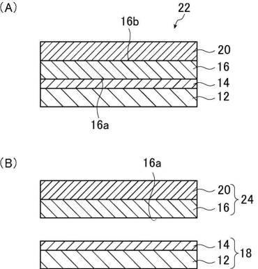
(アルケニル基含有シロキサンの合成)
1,3−ジビニル−1,1,3,3−テトラメチルジシロキサン(3.7g)、1,3,5,7−テトラメチル−1,3,5,7−テトラビニルシクロテトラシロキサン(41.4g)、オクタメチルシクロテトラシロキサン(355.9g)に水酸化カリウムのシリコネートをSi/K=20000/1(mol比)量加え、窒素雰囲気下で150℃、6時間平衡化反応させた。その後、エチレンクロロヒドリンをK(カリウム)に対して2mol量添加し、混合液を120℃で2時間中和した。その後、得られた混合液を160℃、666Paで6時間加熱バブリング処理して、揮発分をカットして、100gあたりのアルケニル当量数La=0.9、Mw:26,000のアルケニル基含有シロキサンを得た。
(Synthesis of alkenyl group-containing siloxane)
1,3-Divinyl-1,1,3,3-tetramethyldisiloxane (3.7 g), 1,3,5,7-tetramethyl-1,3,5,7-tetravinylcyclotetrasiloxane (41) .4 g), octamethylcyclotetrasiloxane (355.9 g) was added with a siliconate of potassium hydroxide in an amount of Si / K = 20000/1 (mol ratio), and an equilibrium reaction was carried out at 150 ° C. for 6 hours in a nitrogen atmosphere. Then, 2 mol of ethylene chlorohydrin was added to K (potassium), and the mixed solution was neutralized at 120 ° C. for 2 hours. Then, the obtained mixed solution was heated and bubbled at 160 ° C. and 666 Pa for 6 hours to cut off volatile components, and the alkenyl equivalent number La = 0.9 per 100 g and Mw: 26,000 alkenyl group-containing siloxane. Got
(硬化性シリコーン2の調製)
オルガノハイドロジェンシロキサンとアルケニル基含有シロキサンとを、全アルケニル基と全ケイ素原子に結合した水素原子とのモル比(水素原子/アルケニル基)が0.9となるように混合することにより、硬化性シリコーン2を得た。
この硬化性シリコーン2(100質量部)に、下記式(2)で示されるアセチレン系不飽和基を有するケイ素化合物(1質量部)を混合し、白金元素の含有量が100ppmとなるように白金触媒を加えて、混合物Aを得た。
HC≡C−C(CH3)2−O−Si(CH3)3 (2)
(Preparation of curable silicone 2)
Curability by mixing organohydrogensiloxane and alkenyl group-containing siloxane so that the molar ratio (hydrogen atom / alkenyl group) of all alkenyl groups and hydrogen atoms bonded to all silicon atoms is 0.9.
This curable silicone 2 (100 parts by mass) is mixed with a silicon compound (1 part by mass) having an acetylene-based unsaturated group represented by the following formula (2), and platinum is prepared so that the content of the platinum element is 100 ppm. A catalyst was added to give mixture A.
HC≡CC (CH 3 ) 2- O-Si (CH 3 ) 3 (2)
(硬化性組成物2の調製)
混合物A(50g)と、金属化合物としてジルコニウムテトラノルマルプロポキシド(「オルガチックスZA−45」、マツモトファインケミカル株式会社製、金属含有率21.1%)(0.71g)と、溶媒としてPMX−0244(東レダウコーニング株式会社製)(50g)とを混合し、得られた混合液を、孔径0.45μmのフィルタを用いてろ過することにより、硬化性組成物2を得た。
(Preparation of curable composition 2)
Mixture A (50 g), zirconium tetranormal propoxide (“Organix ZA-45”, manufactured by Matsumoto Fine Chemicals Co., Ltd., metal content 21.1%) (0.71 g) as a metal compound, and PMX-0244 as a solvent. (Made by Toray Dow Corning Co., Ltd.) (50 g) was mixed, and the obtained mixed solution was filtered using a filter having a pore size of 0.45 μm to obtain a
(ガラス積層体の作製)
得られた硬化性組成物2を、200×200mm、厚み0.5mmの支持基材にスピンコート法により塗布し、ホットプレートを用いて140℃で10分間加熱した。その後、オーブンを用いて大気下220℃で30分間加熱し、膜厚8μmのシリコーン樹脂層を形成した。
その後、200×200mm、厚み0.2mmのガラス基板をシリコーン樹脂層上に置き、貼合装置を用いて貼り合わせ、ガラス積層体を作製した。
(Preparation of glass laminate)
The obtained
Then, a glass substrate having a size of 200 × 200 mm and a thickness of 0.2 mm was placed on a silicone resin layer and bonded using a bonding device to prepare a glass laminate.
<例19>
金属化合物としてテトラノルマルブチルチタネート(「オルガチックス TA−21」、マツモトファインケミカル株式会社製、金属含有率14.1%)を用いたこと、および、金属化合物の添加量を1.06gとしたこと以外は、例18と同様にして、硬化性組成物を作製した。得られた硬化性組成物を、200×200mm、厚み0.5mmの支持基材にスピンコート法により塗布し、ホットプレートを用いて140℃で10分間加熱した。その後、オーブンを用いて大気下220℃で30分間加熱し、膜厚8μmのシリコーン樹脂層を形成した。
その後、200×200mm、厚み0.2mmのガラス基板をシリコーン樹脂層上に置き、貼合装置を用いて貼り合わせ、ガラス積層体を作製した。
<Example 19>
Except that tetranormal butyl titanate (“Organix TA-21”, manufactured by Matsumoto Fine Chemical Co., Ltd., metal content 14.1%) was used as the metal compound, and the amount of the metal compound added was 1.06 g. Made a curable composition in the same manner as in Example 18. The obtained curable composition was applied to a supporting substrate having a thickness of 200 × 200 mm and a thickness of 0.5 mm by a spin coating method, and heated at 140 ° C. for 10 minutes using a hot plate. Then, it was heated in the atmosphere at 220 ° C. for 30 minutes using an oven to form a silicone resin layer having a film thickness of 8 μm.
Then, a glass substrate having a size of 200 × 200 mm and a thickness of 0.2 mm was placed on a silicone resin layer and bonded using a bonding device to prepare a glass laminate.
<例20>
例3と同様の手順で調製した硬化性組成物を、200×200mm、厚み0.5mmの支持基材にスピンコート法により塗布し、ホットプレートを用いて100℃で10分間加熱した。その後、オーブンを用いて大気下250℃で30分間加熱し、膜厚4μmのシリコーン樹脂層を形成した。
その後、厚み0.038mmのポリイミドフィルム(東洋紡株式会社製商品名「ゼノマックス」)を、シリコーン樹脂層上に置き、貼合装置を用いて貼り合わせ、樹脂積層体を作製した。
<Example 20>
The curable composition prepared in the same procedure as in Example 3 was applied to a supporting substrate having a thickness of 200 × 200 mm and a thickness of 0.5 mm by a spin coating method, and heated at 100 ° C. for 10 minutes using a hot plate. Then, it was heated in the atmosphere at 250 ° C. for 30 minutes using an oven to form a silicone resin layer having a film thickness of 4 μm.
Then, a polyimide film having a thickness of 0.038 mm (trade name "Xenomax" manufactured by Toyobo Co., Ltd.) was placed on a silicone resin layer and bonded using a bonding device to prepare a resin laminate.
<例21>
例18と同様の手順で調製した硬化性組成物を、200×200mm、厚み0.5mmの支持基材にスピンコート法により塗布し、ホットプレートを用いて140℃で10分間加熱した。その後、オーブンを用いて大気下220℃で30分間加熱し、膜厚8μmのシリコーン樹脂層を形成した。
その後、厚み0.038mmのポリイミドフィルム(東洋紡株式会社製商品名「ゼノマックス」)を、シリコーン樹脂層上に置き、貼合装置を用いて貼り合わせ、樹脂積層体を作製した。
<Example 21>
The curable composition prepared in the same procedure as in Example 18 was applied to a supporting substrate having a thickness of 200 × 200 mm and a thickness of 0.5 mm by a spin coating method, and heated at 140 ° C. for 10 minutes using a hot plate. Then, it was heated in the atmosphere at 220 ° C. for 30 minutes using an oven to form a silicone resin layer having a film thickness of 8 μm.
Then, a polyimide film having a thickness of 0.038 mm (trade name "Xenomax" manufactured by Toyobo Co., Ltd.) was placed on a silicone resin layer and bonded using a bonding device to prepare a resin laminate.
<例22>
例18と同様の手順で調製した硬化性組成物を、厚み0.038mmのポリイミドフィルム(東洋紡株式会社製商品名「ゼノマックス」)に塗布し、ホットプレートを用いて140℃で10分間加熱した。
次に、200×200mm、厚み0.5mmの支持基材をシリコーン樹脂層上に置き、貼合装置を用いて貼り合わせた。その後、オーブンを用いて大気下220℃で30分間加熱し、樹脂積層体を作製した。
<Example 22>
The curable composition prepared in the same procedure as in Example 18 was applied to a polyimide film having a thickness of 0.038 mm (trade name "Xenomax" manufactured by Toyobo Co., Ltd.) and heated at 140 ° C. for 10 minutes using a hot plate. ..
Next, a supporting base material having a thickness of 200 × 200 mm and a thickness of 0.5 mm was placed on the silicone resin layer and bonded using a bonding device. Then, it was heated in the atmosphere at 220 ° C. for 30 minutes using an oven to prepare a resin laminate.
<例23>
例14と同様の手順で調製した硬化性組成物を、200×200mm、厚み0.5mmの支持基材にスピンコート法により塗布し、ホットプレートを用いて100℃で10分間加熱した。その後、オーブンを用いて大気下250℃で30分間加熱し、膜厚4μmのシリコーン樹脂層を形成した。
その後、厚み0.038mmのポリイミドフィルム(東洋紡株式会社製商品名「ゼノマックス」)を、シリコーン樹脂層上に置き、貼合装置を用いて貼り合わせ、樹脂積層体を作製した。
<Example 23>
The curable composition prepared in the same procedure as in Example 14 was applied to a supporting substrate having a thickness of 200 × 200 mm and a thickness of 0.5 mm by a spin coating method, and heated at 100 ° C. for 10 minutes using a hot plate. Then, it was heated in the atmosphere at 250 ° C. for 30 minutes using an oven to form a silicone resin layer having a film thickness of 4 μm.
Then, a polyimide film having a thickness of 0.038 mm (trade name "Xenomax" manufactured by Toyobo Co., Ltd.) was placed on a silicone resin layer and bonded using a bonding device to prepare a resin laminate.
<例24>
金属化合物としてテトラノルマルブチルチタネート(「オルガチックス TA−21」、マツモトファインケミカル株式会社製、金属含有率14.1%)を用いたこと、および、金属化合物の添加量を1.06gとしたこと以外は、例18と同様にして、硬化性組成物を作製した。作製した硬化性組成物を、200×200mm、厚み0.5mmの支持基材にスピンコート法により塗布し、ホットプレートを用いて140℃で10分間加熱した。その後、オーブンを用いて大気下220℃で30分間加熱し、膜厚8μmのシリコーン樹脂層を形成した。
その後、厚み0.038mmのポリイミドフィルム(東洋紡株式会社製商品名「ゼノマックス」)を、シリコーン樹脂層上に置き、貼合装置を用いて貼り合わせ、樹脂積層体を作製した。
<Example 24>
Except that tetranormal butyl titanate (“Organix TA-21”, manufactured by Matsumoto Fine Chemical Co., Ltd., metal content 14.1%) was used as the metal compound, and the amount of the metal compound added was 1.06 g. Made a curable composition in the same manner as in Example 18. The prepared curable composition was applied to a supporting substrate having a thickness of 200 × 200 mm and a thickness of 0.5 mm by a spin coating method, and heated at 140 ° C. for 10 minutes using a hot plate. Then, it was heated in the atmosphere at 220 ° C. for 30 minutes using an oven to form a silicone resin layer having a film thickness of 8 μm.
Then, a polyimide film having a thickness of 0.038 mm (trade name "Xenomax" manufactured by Toyobo Co., Ltd.) was placed on a silicone resin layer and bonded using a bonding device to prepare a resin laminate.
<例25>
硬化性シリコーン2(100質量部)に、上述した式(2)で示されるアセチレン系不飽和基を有するケイ素化合物(1質量部)を混合し、白金元素の含有量が100ppmとなるように白金触媒を加えて、混合物Aを得た。
混合物A(50g)と、溶媒としてPMX−0244(東レダウコーニング株式会社製)(50g)とを混合し、得られた混合液を、孔径0.45μmのフィルタを用いてろ過をし、混合物B(硬化性組成物)を得た。
混合物B(硬化性組成物)を、200×200mm、厚み0.5mmの支持基材にスピンコート法により塗布し、ホットプレートを用いて140℃で10分間加熱した。その後、オーブンを用いて大気下220℃で30分間加熱し、膜厚8μmのシリコーン樹脂層を形成した。
その後、厚み0.038mmのポリイミドフィルム(東洋紡株式会社製商品名「ゼノマックス」)を、シリコーン樹脂層上に置き、貼合装置を用いて貼り合わせ、樹脂積層体を作製した。
<Example 25>
A silicon compound (1 part by mass) having an acetylene-based unsaturated group represented by the above formula (2) is mixed with curable silicone 2 (100 parts by mass) to make platinum so that the content of platinum element is 100 ppm. A catalyst was added to give mixture A.
Mixture A (50 g) and PMX-0244 (manufactured by Toray Dow Corning Co., Ltd.) (50 g) as a solvent are mixed, and the obtained mixed solution is filtered using a filter having a pore size of 0.45 μm, and the mixture B is used. (Curable composition) was obtained.
Mixture B (curable composition) was applied to a supporting substrate having a thickness of 200 × 200 mm and a thickness of 0.5 mm by a spin coating method, and heated at 140 ° C. for 10 minutes using a hot plate. Then, it was heated in the atmosphere at 220 ° C. for 30 minutes using an oven to form a silicone resin layer having a film thickness of 8 μm.
Then, a polyimide film having a thickness of 0.038 mm (trade name "Xenomax" manufactured by Toyobo Co., Ltd.) was placed on a silicone resin layer and bonded using a bonding device to prepare a resin laminate.
<例26>
混合物B(硬化性組成物)を、厚み0.038mmのポリイミドフィルム(東洋紡株式会社製商品名「ゼノマックス」)に塗布し、ホットプレートを用いて140℃で10分間加熱した。
次に、200×200mm、厚み0.5mmの支持基材をシリコーン樹脂層上に置き、貼合装置を用いて貼り合わせた。その後、オーブンを用いて大気下220℃で30分間加熱し、樹脂積層体を作製した。
<Example 26>
Mixture B (curable composition) was applied to a polyimide film having a thickness of 0.038 mm (trade name "Xenomax" manufactured by Toyobo Co., Ltd.) and heated at 140 ° C. for 10 minutes using a hot plate.
Next, a supporting base material having a thickness of 200 × 200 mm and a thickness of 0.5 mm was placed on the silicone resin layer and bonded using a bonding device. Then, it was heated in the atmosphere at 220 ° C. for 30 minutes using an oven to prepare a resin laminate.
<耐発泡性の評価>
各例にて得られたガラス積層体および樹脂積層体を切り出して、直径1mm以上の気泡がない15×15mmのサンプルを得た。得られた各サンプルを、赤外線加熱炉に入れ、炉内雰囲気を窒素に置換した。その後、炉内のサンプルの様子を観察しながら、20℃/minの速度で、室温から600℃まで昇温した。昇温中、直径が5mm以上の気泡の発生が認められた温度を、このサンプルの「耐熱温度」とした。
サンプルの耐熱温度から、耐発泡性を下記基準により評価した。「A」〜「D」であれば、耐発泡性に優れると評価できる。・「A」:耐熱温度が600℃以上・「B」:耐熱温度が550℃以上、600℃未満・「C」:耐熱温度が530℃以上、550℃未満・「D」:耐熱温度が500℃以上、530℃未満・「E」:耐熱温度が500℃未満
<Evaluation of foam resistance>
The glass laminate and the resin laminate obtained in each example were cut out to obtain a sample of 15 × 15 mm having no air bubbles having a diameter of 1 mm or more. Each of the obtained samples was placed in an infrared heating furnace, and the atmosphere inside the furnace was replaced with nitrogen. Then, while observing the state of the sample in the furnace, the temperature was raised from room temperature to 600 ° C. at a rate of 20 ° C./min. The temperature at which bubbles having a diameter of 5 mm or more were observed during the temperature rise was defined as the "heat resistant temperature" of this sample.
From the heat resistant temperature of the sample, the foam resistance was evaluated according to the following criteria. If it is "A" to "D", it can be evaluated that the foam resistance is excellent. -"A": heat-resistant temperature is 600 ° C or higher- "B": heat-resistant temperature is 550 ° C or higher and less than 600 ° C- "C": heat-resistant temperature is 530 ° C or higher and lower than 550 ° C- "D": heat-resistant temperature is 500 ℃ or more and less than 530 ℃ ・ "E": Heat resistant temperature is less than 500 ℃
以上の結果を、まとめて下記表1〜表4に示す。
下記表1〜表4には、各例において使用した硬化性シリコーンの種類(硬化性シリコーン1または2)を記載した。
下記表1〜表4には、各例における、シリコーン樹脂層に含まれる金属元素の種類、および、その含有量を記載した。このとき、1種類の場合は「金属元素1」に記載し、「金属元素2」には「−」を記載した。2種類の場合は「金属元素1」および「金属元素2」に記載した。含有量は、シリコーン樹脂層中の金属元素それぞれの含有量(割合)であり、単位は「質量%」であるが、下記表1〜表3においては、単に「%」としている。
さらに、下記表1〜表4には、各例における耐熱温度および耐発泡性の評価結果も記載した。
下記表4にのみ、硬化性組成物を塗布した基板(塗布基板)の商品名を記載した。
The above results are summarized in Tables 1 to 4 below.
Tables 1 to 4 below show the types of curable silicones (curable silicones 1 or 2) used in each example.
Tables 1 to 4 below show the types of metal elements contained in the silicone resin layer and their contents in each example. At this time, in the case of one type, "metal element 1" is described, and "-" is described in "
Further, Tables 1 to 4 below also show the evaluation results of the heat resistant temperature and the foam resistance in each example.
Only in Table 4 below, the trade names of the substrates (coated substrates) coated with the curable composition are listed.
上記表1〜表4に示す結果から明らかなように、シリコーン樹脂層が、ジルコニウム(Zr)、アルミニウム(Al)、および、スズ(Sn)からなる群から選択される少なくとも1種の金属の元素(特定元素)を含む例1〜13および、例17〜18のガラス積層体ならびに、例20〜22の樹脂積層体は、耐発泡性に優れていた。
これに対して、上記特定元素を含まない例14〜16のガラス積層体、例19のガラス積層体、および、例23〜26の樹脂積層体は、耐発泡性が劣っていた。
As is clear from the results shown in Tables 1 to 4, the silicone resin layer is an element of at least one metal selected from the group consisting of zirconium (Zr), aluminum (Al), and tin (Sn). The glass laminates of Examples 1 to 13 and Examples 17 to 18 and the resin laminates of Examples 20 to 22 containing (specific element) were excellent in foam resistance.
On the other hand, the glass laminates of Examples 14 to 16, the glass laminates of Example 19, and the resin laminates of Examples 23 to 26, which do not contain the specific element, were inferior in foam resistance.
例2,4,6を対比すると、シリコーン樹脂層がAlまたはSnを含有する例4および6よりも、シリコーン樹脂層がZrを含有する例2の方が、より耐発泡性が良好であった。 Comparing Examples 2, 4 and 6, Example 2 in which the silicone resin layer contained Zr had better foam resistance than Examples 4 and 6 in which the silicone resin layer contained Al or Sn. ..
<例27>
例18で200×200mm、厚み0.2mmのガラス基板の代わりに、直径150mm、厚み625μmのSiウェハを貼り合せた積層体を作製する。この積層体を例18と同じ条件で耐発泡評価を実施したところ、耐発泡性はDである。例27の半導体積層体は耐発泡性に優れる。
<Example 27>
In Example 18, a laminated body is prepared by laminating a Si wafer having a diameter of 150 mm and a thickness of 625 μm instead of a glass substrate having a diameter of 200 × 200 mm and a thickness of 0.2 mm. When the foam resistance of this laminate was evaluated under the same conditions as in Example 18, the foam resistance was D. The semiconductor laminate of Example 27 has excellent foam resistance.
<例28>
例19で200×200mm、厚み0.2mmのガラス基板の代わりに、直径150mm、厚み625μmのSiウェハを貼り合せた積層体を作製する。この積層体を例19と同じ条件で耐発泡評価を実施したところ、耐発泡性はEである。例28の半導体積層体は耐発泡性が劣っている。
<Example 28>
In Example 19, a laminated body is prepared by laminating a Si wafer having a diameter of 150 mm and a thickness of 625 μm instead of a glass substrate having a diameter of 200 × 200 mm and a thickness of 0.2 mm. When the foam resistance of this laminate was evaluated under the same conditions as in Example 19, the foam resistance was E. The semiconductor laminate of Example 28 is inferior in foam resistance.
10 ガラス積層体
12 支持基材
14 シリコーン樹脂層
14a シリコーン樹脂層の表面
16 ガラス基板
16a ガラス基板の第1主面
16b ガラス基板の第2主面
18 シリコーン樹脂層付き支持基材
20 電子デバイス用部材
22 電子デバイス用部材付き積層体
24 部材付き基板(電子デバイス)
10
Claims (13)
前記シリコーン樹脂層が、ジルコニウム、および、スズからなる群から選択される少なくとも1種の金属の元素を含み、
前記支持基材がガラス板または金属板からなる、積層体。 A support base material, a silicone resin layer, and a substrate are provided in this order.
The silicone resin layer contains zirconium, you and, at least one metal element selected from the group consisting of tin,
A laminate in which the supporting base material is a glass plate or a metal plate.
前記シリコーン樹脂層が、ジルコニウム、および、スズからなる群から選択される少なくとも1種の金属の元素を含み、
前記支持基材がガラス板または金属板からなる、シリコーン樹脂層付き支持基材。 A support base material and a silicone resin layer are provided in this order.
The silicone resin layer contains zirconium, you and, at least one metal element selected from the group consisting of tin,
A support base material with a silicone resin layer, wherein the support base material is a glass plate or a metal plate.
前記電子デバイス用部材付き積層体から前記支持基材および前記シリコーン樹脂層を含むシリコーン樹脂層付き支持基材を除去し、前記基板と前記電子デバイス用部材とを有する電子デバイスを得る分離工程と、を備える電子デバイスの製造方法。 A member forming step of forming a member for an electronic device on the surface of the substrate of the laminate according to any one of claims 1 to 9 to obtain a laminate with a member for an electronic device.
A separation step of removing the support base material and the support base material with a silicone resin layer including the silicone resin layer from the laminate with the member for the electronic device to obtain an electronic device having the substrate and the member for the electronic device. A method of manufacturing an electronic device comprising.
前記シリコーン樹脂層が、ジルコニウム、アルミニウム、および、スズからなる群から選択される少なくとも1種の金属の元素を含む、シリコーン樹脂層付き樹脂基板。 A resin substrate and a silicone resin layer are provided in this order.
A resin substrate with a silicone resin layer, wherein the silicone resin layer contains an element of at least one metal selected from the group consisting of zirconium, aluminum, and tin.
前記積層体の前記樹脂基板の表面上に電子デバイス用部材を形成し、電子デバイス用部材付き積層体を得る部材形成工程と、
前記電子デバイス用部材付き積層体から前記支持基材および前記シリコーン樹脂層を除去し、前記樹脂基板と前記電子デバイス用部材とを有する電子デバイスを得る分離工程と、を備える電子デバイスの製造方法。 A step of forming a laminate by using the resin substrate with a silicone resin layer according to claim 12 and a supporting base material.
A member forming step of forming a member for an electronic device on the surface of the resin substrate of the laminated body to obtain a laminated body with a member for an electronic device.
A method for manufacturing an electronic device, comprising a separation step of removing the supporting base material and the silicone resin layer from the laminate with a member for an electronic device to obtain an electronic device having the resin substrate and the member for the electronic device.
Priority Applications (7)
| Application Number | Priority Date | Filing Date | Title |
|---|---|---|---|
| TW112122706A TWI890079B (en) | 2016-12-28 | 2017-12-26 | Hardening composition, laminate, and glass agglomerated with silicone resin layer |
| TW106145741A TWI808956B (en) | 2016-12-28 | 2017-12-26 | Laminate, supporting base material of agglomerated silicone resin layer, resin substrate of agglomerated silicone resin layer, and manufacturing method of electronic device |
| CN201711435286.6A CN108248155B (en) | 2016-12-28 | 2017-12-26 | Laminate, supporting base material with silicone resin layer, resin substrate with silicone resin layer, and method for manufacturing electronic device |
| CN202310160807.0A CN116285864B (en) | 2016-12-28 | 2017-12-26 | Laminated body, supporting base material with silicone resin layer, resin substrate with silicone resin layer, and method for producing electronic device |
| KR1020170179823A KR102475941B1 (en) | 2016-12-28 | 2017-12-26 | Laminate, silicone resin layer-attached support substrate, silicone resin layer-attached resin substrate, and method for producing electronic device |
| US15/856,329 US20180178245A1 (en) | 2016-12-28 | 2017-12-28 | Laminate, silicone resin layer-attached support substrate, silicone resin layer-attached resin substrate, and method for producing electronic device |
| KR1020220166922A KR102629661B1 (en) | 2016-12-28 | 2022-12-02 | Laminate, silicone resin layer-attached support substrate, silicone resin layer-attached resin substrate, and method for producing electronic device |
Applications Claiming Priority (4)
| Application Number | Priority Date | Filing Date | Title |
|---|---|---|---|
| JP2016255206 | 2016-12-28 | ||
| JP2016255206 | 2016-12-28 | ||
| JP2017120689 | 2017-06-20 | ||
| JP2017120689 | 2017-06-20 |
Publications (2)
| Publication Number | Publication Date |
|---|---|
| JP2018202849A JP2018202849A (en) | 2018-12-27 |
| JP6946900B2 true JP6946900B2 (en) | 2021-10-13 |
Family
ID=64956136
Family Applications (1)
| Application Number | Title | Priority Date | Filing Date |
|---|---|---|---|
| JP2017185777A Active JP6946900B2 (en) | 2016-12-28 | 2017-09-27 | Method for manufacturing laminate, support base material with silicone resin layer, resin substrate with silicone resin layer, and electronic device |
Country Status (1)
| Country | Link |
|---|---|
| JP (1) | JP6946900B2 (en) |
Families Citing this family (3)
| Publication number | Priority date | Publication date | Assignee | Title |
|---|---|---|---|---|
| JP7115510B2 (en) * | 2019-06-06 | 2022-08-09 | Agc株式会社 | Laminated substrate and package |
| WO2021015057A1 (en) | 2019-07-25 | 2021-01-28 | Agc株式会社 | Layered member |
| WO2021015059A1 (en) | 2019-07-25 | 2021-01-28 | Agc株式会社 | Laminated member |
Family Cites Families (8)
| Publication number | Priority date | Publication date | Assignee | Title |
|---|---|---|---|---|
| JPH09131842A (en) * | 1995-11-13 | 1997-05-20 | Teijin Ltd | Laminated film |
| JP4849814B2 (en) * | 2005-03-29 | 2012-01-11 | 東レ・ダウコーニング株式会社 | Hot-melt silicone adhesive |
| JP2009024127A (en) * | 2007-07-23 | 2009-02-05 | Three M Innovative Properties Co | Method for sealing air bag inflator, silicone-based pressure-sensitive adhesive tape and air bag inflator |
| JP5729253B2 (en) * | 2011-10-17 | 2015-06-03 | 信越化学工業株式会社 | Condensation reaction curable silicone release coating composition |
| CN103946227B (en) * | 2011-12-02 | 2017-09-26 | Cp菲林公司 | Catalyst for Thermally Cured Silicone Release Coatings |
| CN104603226B (en) * | 2012-09-05 | 2017-03-15 | 信越聚合物株式会社 | Antistatic release agent and antistatic release film |
| JP6402009B2 (en) * | 2014-11-20 | 2018-10-10 | アイカ工業株式会社 | Peelable silicone resin composition and release film coated with the same |
| JP6773569B2 (en) * | 2016-02-15 | 2020-10-21 | 三洋化成工業株式会社 | Antistatic silicone resin composition |
-
2017
- 2017-09-27 JP JP2017185777A patent/JP6946900B2/en active Active
Also Published As
| Publication number | Publication date |
|---|---|
| JP2018202849A (en) | 2018-12-27 |
Similar Documents
| Publication | Publication Date | Title |
|---|---|---|
| KR102635001B1 (en) | Laminate, silicone resin layer-attached support substrate, silicone resin layer-attached resin substrate, and method for producing electronic device | |
| KR102629661B1 (en) | Laminate, silicone resin layer-attached support substrate, silicone resin layer-attached resin substrate, and method for producing electronic device | |
| JP7099478B2 (en) | Laminates, methods for manufacturing laminates, and methods for manufacturing electronic devices | |
| JP6443350B2 (en) | Glass laminate | |
| JP6927203B2 (en) | Glass laminate and its manufacturing method | |
| JP6946901B2 (en) | Method for manufacturing laminate, support base material with silicone resin layer, resin substrate with silicone resin layer, electronic device | |
| JP6471643B2 (en) | Glass laminate and method for producing the same | |
| JP6946900B2 (en) | Method for manufacturing laminate, support base material with silicone resin layer, resin substrate with silicone resin layer, and electronic device | |
| WO2014050833A1 (en) | Glass laminate and manufacturing method for same, and support substrate having silicone resin layer attached thereto and manufacturing method for same | |
| JP7102899B2 (en) | Manufacturing method of laminates and electronic devices |
Legal Events
| Date | Code | Title | Description |
|---|---|---|---|
| A621 | Written request for application examination |
Free format text: JAPANESE INTERMEDIATE CODE: A621 Effective date: 20200206 |
|
| RD04 | Notification of resignation of power of attorney |
Free format text: JAPANESE INTERMEDIATE CODE: A7424 Effective date: 20200701 |
|
| A977 | Report on retrieval |
Free format text: JAPANESE INTERMEDIATE CODE: A971007 Effective date: 20201111 |
|
| A131 | Notification of reasons for refusal |
Free format text: JAPANESE INTERMEDIATE CODE: A131 Effective date: 20201201 |
|
| A521 | Request for written amendment filed |
Free format text: JAPANESE INTERMEDIATE CODE: A523 Effective date: 20210106 |
|
| A131 | Notification of reasons for refusal |
Free format text: JAPANESE INTERMEDIATE CODE: A131 Effective date: 20210406 |
|
| A521 | Request for written amendment filed |
Free format text: JAPANESE INTERMEDIATE CODE: A523 Effective date: 20210521 |
|
| TRDD | Decision of grant or rejection written | ||
| A01 | Written decision to grant a patent or to grant a registration (utility model) |
Free format text: JAPANESE INTERMEDIATE CODE: A01 Effective date: 20210817 |
|
| A61 | First payment of annual fees (during grant procedure) |
Free format text: JAPANESE INTERMEDIATE CODE: A61 Effective date: 20210830 |
|
| R150 | Certificate of patent or registration of utility model |
Ref document number: 6946900 Country of ref document: JP Free format text: JAPANESE INTERMEDIATE CODE: R150 |
|
| R250 | Receipt of annual fees |
Free format text: JAPANESE INTERMEDIATE CODE: R250 |
|
| R250 | Receipt of annual fees |
Free format text: JAPANESE INTERMEDIATE CODE: R250 |