JP6917234B2 - Integrated circuits and methods for manufacturing integrated circuits - Google Patents
Integrated circuits and methods for manufacturing integrated circuits Download PDFInfo
- Publication number
- JP6917234B2 JP6917234B2 JP2017144864A JP2017144864A JP6917234B2 JP 6917234 B2 JP6917234 B2 JP 6917234B2 JP 2017144864 A JP2017144864 A JP 2017144864A JP 2017144864 A JP2017144864 A JP 2017144864A JP 6917234 B2 JP6917234 B2 JP 6917234B2
- Authority
- JP
- Japan
- Prior art keywords
- transistor
- region
- concentration
- transistors
- differential pair
- Prior art date
- Legal status (The legal status is an assumption and is not a legal conclusion. Google has not performed a legal analysis and makes no representation as to the accuracy of the status listed.)
- Active
Links
- 238000004519 manufacturing process Methods 0.000 title claims description 98
- 238000000034 method Methods 0.000 title claims description 66
- 239000012535 impurity Substances 0.000 claims description 505
- 150000002500 ions Chemical class 0.000 claims description 110
- 238000005468 ion implantation Methods 0.000 claims description 70
- 239000000758 substrate Substances 0.000 claims description 61
- 239000004065 semiconductor Substances 0.000 claims description 33
- 238000002955 isolation Methods 0.000 claims description 5
- 239000010410 layer Substances 0.000 description 449
- 238000012937 correction Methods 0.000 description 40
- 239000003990 capacitor Substances 0.000 description 34
- XUIMIQQOPSSXEZ-UHFFFAOYSA-N Silicon Chemical compound [Si] XUIMIQQOPSSXEZ-UHFFFAOYSA-N 0.000 description 33
- 229910052710 silicon Inorganic materials 0.000 description 33
- 239000010703 silicon Substances 0.000 description 32
- 238000000926 separation method Methods 0.000 description 28
- 230000000694 effects Effects 0.000 description 22
- 239000002344 surface layer Substances 0.000 description 20
- 229910052814 silicon oxide Inorganic materials 0.000 description 19
- VYPSYNLAJGMNEJ-UHFFFAOYSA-N Silicium dioxide Chemical compound O=[Si]=O VYPSYNLAJGMNEJ-UHFFFAOYSA-N 0.000 description 18
- -1 arsenic ions Chemical class 0.000 description 18
- 230000008569 process Effects 0.000 description 17
- 238000010586 diagram Methods 0.000 description 14
- 229910052796 boron Inorganic materials 0.000 description 10
- 229910017052 cobalt Inorganic materials 0.000 description 10
- 239000010941 cobalt Substances 0.000 description 10
- GUTLYIVDDKVIGB-UHFFFAOYSA-N cobalt atom Chemical compound [Co] GUTLYIVDDKVIGB-UHFFFAOYSA-N 0.000 description 10
- 230000007423 decrease Effects 0.000 description 10
- 239000000463 material Substances 0.000 description 9
- 150000004767 nitrides Chemical class 0.000 description 9
- 230000003321 amplification Effects 0.000 description 8
- 230000004048 modification Effects 0.000 description 8
- 238000012986 modification Methods 0.000 description 8
- 238000003199 nucleic acid amplification method Methods 0.000 description 8
- 229910052698 phosphorus Inorganic materials 0.000 description 8
- 239000011574 phosphorus Substances 0.000 description 8
- 238000004335 scaling law Methods 0.000 description 8
- 101100243558 Caenorhabditis elegans pfd-3 gene Proteins 0.000 description 7
- 238000005530 etching Methods 0.000 description 7
- 238000005229 chemical vapour deposition Methods 0.000 description 6
- 239000011229 interlayer Substances 0.000 description 6
- HAYXDMNJJFVXCI-UHFFFAOYSA-N arsenic(5+) Chemical compound [As+5] HAYXDMNJJFVXCI-UHFFFAOYSA-N 0.000 description 5
- 230000003647 oxidation Effects 0.000 description 5
- 238000007254 oxidation reaction Methods 0.000 description 5
- 238000000206 photolithography Methods 0.000 description 5
- 229910021332 silicide Inorganic materials 0.000 description 5
- FVBUAEGBCNSCDD-UHFFFAOYSA-N silicide(4-) Chemical compound [Si-4] FVBUAEGBCNSCDD-UHFFFAOYSA-N 0.000 description 5
- ATJFFYVFTNAWJD-UHFFFAOYSA-N Tin Chemical compound [Sn] ATJFFYVFTNAWJD-UHFFFAOYSA-N 0.000 description 4
- 238000006243 chemical reaction Methods 0.000 description 4
- 238000010438 heat treatment Methods 0.000 description 4
- 238000002347 injection Methods 0.000 description 4
- 239000007924 injection Substances 0.000 description 4
- 229910021420 polycrystalline silicon Inorganic materials 0.000 description 4
- 229920005591 polysilicon Polymers 0.000 description 4
- ZOXJGFHDIHLPTG-UHFFFAOYSA-N Boron Chemical compound [B] ZOXJGFHDIHLPTG-UHFFFAOYSA-N 0.000 description 3
- 229910052581 Si3N4 Inorganic materials 0.000 description 3
- 229910052782 aluminium Inorganic materials 0.000 description 3
- 230000015572 biosynthetic process Effects 0.000 description 3
- 239000000470 constituent Substances 0.000 description 3
- 230000006870 function Effects 0.000 description 3
- 230000010354 integration Effects 0.000 description 3
- HQVNEWCFYHHQES-UHFFFAOYSA-N silicon nitride Chemical compound N12[Si]34N5[Si]62N3[Si]51N64 HQVNEWCFYHHQES-UHFFFAOYSA-N 0.000 description 3
- 229910004298 SiO 2 Inorganic materials 0.000 description 2
- XAGFODPZIPBFFR-UHFFFAOYSA-N aluminium Chemical compound [Al] XAGFODPZIPBFFR-UHFFFAOYSA-N 0.000 description 2
- 229910052785 arsenic Inorganic materials 0.000 description 2
- 230000000052 comparative effect Effects 0.000 description 2
- 230000009467 reduction Effects 0.000 description 2
- 239000000126 substance Substances 0.000 description 2
- 238000012546 transfer Methods 0.000 description 2
- 229910018072 Al 2 O 3 Inorganic materials 0.000 description 1
- 229910020203 CeO Inorganic materials 0.000 description 1
- 229910021193 La 2 O 3 Inorganic materials 0.000 description 1
- OAICVXFJPJFONN-UHFFFAOYSA-N Phosphorus Chemical compound [P] OAICVXFJPJFONN-UHFFFAOYSA-N 0.000 description 1
- 229910010413 TiO 2 Inorganic materials 0.000 description 1
- 230000003213 activating effect Effects 0.000 description 1
- 229910045601 alloy Inorganic materials 0.000 description 1
- 239000000956 alloy Substances 0.000 description 1
- 238000000137 annealing Methods 0.000 description 1
- 238000013459 approach Methods 0.000 description 1
- 230000008859 change Effects 0.000 description 1
- 239000013078 crystal Substances 0.000 description 1
- 230000007547 defect Effects 0.000 description 1
- 230000006866 deterioration Effects 0.000 description 1
- 238000005516 engineering process Methods 0.000 description 1
- 229910052735 hafnium Inorganic materials 0.000 description 1
- 230000006872 improvement Effects 0.000 description 1
- 239000012212 insulator Substances 0.000 description 1
- 239000004973 liquid crystal related substance Substances 0.000 description 1
- 239000000203 mixture Substances 0.000 description 1
- 229910052750 molybdenum Inorganic materials 0.000 description 1
- LIVNPJMFVYWSIS-UHFFFAOYSA-N silicon monoxide Chemical compound [Si-]#[O+] LIVNPJMFVYWSIS-UHFFFAOYSA-N 0.000 description 1
- 239000002356 single layer Substances 0.000 description 1
- 238000000638 solvent extraction Methods 0.000 description 1
- 229910052715 tantalum Inorganic materials 0.000 description 1
- 229910052719 titanium Inorganic materials 0.000 description 1
- 229910052726 zirconium Inorganic materials 0.000 description 1
Images


Classifications
-
- H—ELECTRICITY
- H03—ELECTRONIC CIRCUITRY
- H03F—AMPLIFIERS
- H03F3/00—Amplifiers with only discharge tubes or only semiconductor devices as amplifying elements
- H03F3/45—Differential amplifiers
- H03F3/45071—Differential amplifiers with semiconductor devices only
- H03F3/45076—Differential amplifiers with semiconductor devices only characterised by the way of implementation of the active amplifying circuit in the differential amplifier
- H03F3/45179—Differential amplifiers with semiconductor devices only characterised by the way of implementation of the active amplifying circuit in the differential amplifier using MOSFET transistors as the active amplifying circuit
- H03F3/45183—Long tailed pairs
-
- H—ELECTRICITY
- H01—ELECTRIC ELEMENTS
- H01L—SEMICONDUCTOR DEVICES NOT COVERED BY CLASS H10
- H01L21/00—Processes or apparatus adapted for the manufacture or treatment of semiconductor or solid state devices or of parts thereof
- H01L21/70—Manufacture or treatment of devices consisting of a plurality of solid state components formed in or on a common substrate or of parts thereof; Manufacture of integrated circuit devices or of parts thereof
- H01L21/71—Manufacture of specific parts of devices defined in group H01L21/70
- H01L21/76—Making of isolation regions between components
- H01L21/762—Dielectric regions, e.g. EPIC dielectric isolation, LOCOS; Trench refilling techniques, SOI technology, use of channel stoppers
- H01L21/76224—Dielectric regions, e.g. EPIC dielectric isolation, LOCOS; Trench refilling techniques, SOI technology, use of channel stoppers using trench refilling with dielectric materials
- H01L21/76227—Dielectric regions, e.g. EPIC dielectric isolation, LOCOS; Trench refilling techniques, SOI technology, use of channel stoppers using trench refilling with dielectric materials the dielectric materials being obtained by full chemical transformation of non-dielectric materials, such as polycristalline silicon, metals
-
- H—ELECTRICITY
- H01—ELECTRIC ELEMENTS
- H01L—SEMICONDUCTOR DEVICES NOT COVERED BY CLASS H10
- H01L21/00—Processes or apparatus adapted for the manufacture or treatment of semiconductor or solid state devices or of parts thereof
- H01L21/70—Manufacture or treatment of devices consisting of a plurality of solid state components formed in or on a common substrate or of parts thereof; Manufacture of integrated circuit devices or of parts thereof
- H01L21/71—Manufacture of specific parts of devices defined in group H01L21/70
- H01L21/76—Making of isolation regions between components
- H01L21/762—Dielectric regions, e.g. EPIC dielectric isolation, LOCOS; Trench refilling techniques, SOI technology, use of channel stoppers
- H01L21/76224—Dielectric regions, e.g. EPIC dielectric isolation, LOCOS; Trench refilling techniques, SOI technology, use of channel stoppers using trench refilling with dielectric materials
- H01L21/76229—Concurrent filling of a plurality of trenches having a different trench shape or dimension, e.g. rectangular and V-shaped trenches, wide and narrow trenches, shallow and deep trenches
-
- H—ELECTRICITY
- H03—ELECTRONIC CIRCUITRY
- H03F—AMPLIFIERS
- H03F3/00—Amplifiers with only discharge tubes or only semiconductor devices as amplifying elements
- H03F3/30—Single-ended push-pull [SEPP] amplifiers; Phase-splitters therefor
- H03F3/3001—Single-ended push-pull [SEPP] amplifiers; Phase-splitters therefor with field-effect transistors
- H03F3/3022—CMOS common source output SEPP amplifiers
-
- H—ELECTRICITY
- H10—SEMICONDUCTOR DEVICES; ELECTRIC SOLID-STATE DEVICES NOT OTHERWISE PROVIDED FOR
- H10D—INORGANIC ELECTRIC SEMICONDUCTOR DEVICES
- H10D84/00—Integrated devices formed in or on semiconductor substrates that comprise only semiconducting layers, e.g. on Si wafers or on GaAs-on-Si wafers
- H10D84/01—Manufacture or treatment
- H10D84/0107—Integrating at least one component covered by H10D12/00 or H10D30/00 with at least one component covered by H10D8/00, H10D10/00 or H10D18/00, e.g. integrating IGFETs with BJTs
- H10D84/0109—Integrating at least one component covered by H10D12/00 or H10D30/00 with at least one component covered by H10D8/00, H10D10/00 or H10D18/00, e.g. integrating IGFETs with BJTs the at least one component covered by H10D12/00 or H10D30/00 being a MOS device
-
- H—ELECTRICITY
- H10—SEMICONDUCTOR DEVICES; ELECTRIC SOLID-STATE DEVICES NOT OTHERWISE PROVIDED FOR
- H10D—INORGANIC ELECTRIC SEMICONDUCTOR DEVICES
- H10D84/00—Integrated devices formed in or on semiconductor substrates that comprise only semiconducting layers, e.g. on Si wafers or on GaAs-on-Si wafers
- H10D84/01—Manufacture or treatment
- H10D84/0123—Integrating together multiple components covered by H10D12/00 or H10D30/00, e.g. integrating multiple IGBTs
- H10D84/0126—Integrating together multiple components covered by H10D12/00 or H10D30/00, e.g. integrating multiple IGBTs the components including insulated gates, e.g. IGFETs
- H10D84/0128—Manufacturing their channels
-
- H—ELECTRICITY
- H10—SEMICONDUCTOR DEVICES; ELECTRIC SOLID-STATE DEVICES NOT OTHERWISE PROVIDED FOR
- H10D—INORGANIC ELECTRIC SEMICONDUCTOR DEVICES
- H10D84/00—Integrated devices formed in or on semiconductor substrates that comprise only semiconducting layers, e.g. on Si wafers or on GaAs-on-Si wafers
- H10D84/01—Manufacture or treatment
- H10D84/02—Manufacture or treatment characterised by using material-based technologies
- H10D84/03—Manufacture or treatment characterised by using material-based technologies using Group IV technology, e.g. silicon technology or silicon-carbide [SiC] technology
- H10D84/038—Manufacture or treatment characterised by using material-based technologies using Group IV technology, e.g. silicon technology or silicon-carbide [SiC] technology using silicon technology, e.g. SiGe
-
- H—ELECTRICITY
- H10—SEMICONDUCTOR DEVICES; ELECTRIC SOLID-STATE DEVICES NOT OTHERWISE PROVIDED FOR
- H10B—ELECTRONIC MEMORY DEVICES
- H10B10/00—Static random access memory [SRAM] devices
- H10B10/12—Static random access memory [SRAM] devices comprising a MOSFET load element
-
- H—ELECTRICITY
- H10—SEMICONDUCTOR DEVICES; ELECTRIC SOLID-STATE DEVICES NOT OTHERWISE PROVIDED FOR
- H10B—ELECTRONIC MEMORY DEVICES
- H10B10/00—Static random access memory [SRAM] devices
- H10B10/18—Peripheral circuit regions
Landscapes
- Engineering & Computer Science (AREA)
- Power Engineering (AREA)
- Physics & Mathematics (AREA)
- Condensed Matter Physics & Semiconductors (AREA)
- General Physics & Mathematics (AREA)
- Manufacturing & Machinery (AREA)
- Computer Hardware Design (AREA)
- Microelectronics & Electronic Packaging (AREA)
- Metal-Oxide And Bipolar Metal-Oxide Semiconductor Integrated Circuits (AREA)
- Amplifiers (AREA)
Description
本発明は、集積回路及び集積回路の製造方法に関する。 The present invention relates to integrated circuits and methods for manufacturing integrated circuits.
オペアンプ等の集積回路は、様々な電子機器に用いられている。例えば特許文献1に記載のオペアンプは、液晶駆動装置に用いられている。
Integrated circuits such as operational amplifiers are used in various electronic devices. For example, the operational amplifier described in
近年、集積回路のトランジスタの微細化が進められている。これに伴い、集積回路の1/fノイズ(フリッカノイズ)が悪化する場合がある。このため、集積回路の1/fノイズの改善が望まれている。 In recent years, the miniaturization of transistors in integrated circuits has been promoted. Along with this, 1 / f noise (flicker noise) of the integrated circuit may be deteriorated. Therefore, improvement of 1 / f noise of integrated circuits is desired.
本発明の目的は、1/fノイズを低減できる集積回路及び集積回路の製造方法を提供することにある。 An object of the present invention is to provide an integrated circuit capable of reducing 1 / f noise and a method for manufacturing the integrated circuit.
〔1〕上記課題を解決する集積回路は、微細化された複数のトランジスタを含む集積回路であって、前記複数のトランジスタは、チャネル領域の不純物濃度が第1濃度である高濃度トランジスタと、チャネル領域の不純物濃度が前記第1濃度よりも低い第2濃度である低濃度トランジスタと、を含む。 [1] An integrated circuit that solves the above problems is an integrated circuit that includes a plurality of miniaturized transistors, and the plurality of transistors include a high-concentration transistor having a first concentration of impurities in the channel region and a channel. It includes a low-concentration transistor having a second concentration in which the impurity concentration in the region is lower than the first concentration.
この構成によれば、トランジスタにおけるチャネル領域の不純物濃度が低くなることにより、移動度の揺らぎを抑制できるため、ドレイン電流の揺らぎを抑制できる。ドレイン電流の揺らぎは、集積回路の1/fノイズの大きさと相関を有するため、ドレイン電流の揺らぎを抑制することにより、集積回路の1/fノイズを低減できる。 According to this configuration, the fluctuation of the mobility can be suppressed by lowering the impurity concentration in the channel region of the transistor, so that the fluctuation of the drain current can be suppressed. Since the fluctuation of the drain current has a correlation with the magnitude of the 1 / f noise of the integrated circuit, the 1 / f noise of the integrated circuit can be reduced by suppressing the fluctuation of the drain current.
〔2〕上記集積回路において、前記低濃度トランジスタは、前記高濃度トランジスタよりも、前記複数のトランジスタのうち前記集積回路の1/fノイズの影響を受け易いトランジスタに用いられていることが好ましい。 [2] In the integrated circuit, it is preferable that the low-concentration transistor is used for a transistor among the plurality of transistors that is more susceptible to 1 / f noise of the integrated circuit than the high-concentration transistor.
この構成によれば、集積回路における1/fノイズの影響を受け易いトランジスタにおけるチャネル領域の不純物濃度を低くすることにより、そのトランジスタの移動度の揺らぎを抑制でき、ドレイン電流の揺らぎを抑制できる。したがって、集積回路の1/fノイズを効果的に低減できる。 According to this configuration, by lowering the impurity concentration in the channel region of the transistor that is easily affected by 1 / f noise in the integrated circuit, the fluctuation of the mobility of the transistor can be suppressed, and the fluctuation of the drain current can be suppressed. Therefore, 1 / f noise of the integrated circuit can be effectively reduced.
〔3〕上記集積回路において、前記複数のトランジスタは、STI(Shallow Trench Isolation)構造が用いられていることが好ましい。
〔4〕上記集積回路において、前記集積回路は、オペアンプを含み、前記オペアンプは、差動対を含み、前記複数のトランジスタのうちの前記差動対を構成するトランジスタは、前記低濃度トランジスタであることが好ましい。
[3] In the integrated circuit, it is preferable that the plurality of transistors have an STI (Shallow Trench Isolation) structure.
[4] In the integrated circuit, the integrated circuit includes an operational amplifier, the operational amplifier includes a differential pair, and the transistor constituting the differential pair among the plurality of transistors is the low concentration transistor. Is preferable.
この構成によれば、集積回路において1/fノイズの影響を受け易い差動対を構成するトランジスタにおけるチャネル領域の不純物濃度を低くすることにより、集積回路の1/fノイズを効果的に低減できる。 According to this configuration, the 1 / f noise of the integrated circuit can be effectively reduced by lowering the impurity concentration in the channel region of the transistors forming the differential pair which is easily affected by the 1 / f noise in the integrated circuit. ..
〔5〕上記集積回路において、前記オペアンプは、カレントミラー回路を含み、前記複数のトランジスタのうちの前記カレントミラー回路を構成するトランジスタは、前記低濃度トランジスタであることが好ましい。 [5] In the integrated circuit, the operational amplifier preferably includes a current mirror circuit, and the transistor constituting the current mirror circuit among the plurality of transistors is preferably the low concentration transistor.
この構成によれば、集積回路において1/fノイズの影響を受け易いカレントミラー回路を構成するトランジスタにおけるチャネル領域の不純物濃度を低くすることにより、集積回路の1/fノイズを効果的に低減できる。 According to this configuration, the 1 / f noise of the integrated circuit can be effectively reduced by lowering the impurity concentration in the channel region of the transistor constituting the current mirror circuit which is easily affected by the 1 / f noise in the integrated circuit. ..
〔6〕上記集積回路において、前記カレントミラー回路を構成するトランジスタは、エンハンスメント型MOSFETであることが好ましい。
〔7〕上記集積回路において、前記オペアンプは、最終段を含み、前記複数のトランジスタのうちの前記最終段を構成するトランジスタは、前記高濃度トランジスタであることが好ましい。
[6] In the integrated circuit, the transistor constituting the current mirror circuit is preferably an enhancement type MOSFET.
[7] In the integrated circuit, the operational amplifier preferably includes the final stage, and the transistor constituting the final stage among the plurality of transistors is preferably the high concentration transistor.
この構成によれば、集積回路の駆動電流に寄与する最終段のトランジスタにおけるチャネル領域の不純物濃度を低くしないことにより、そのトランジスタのしきい値の変動を抑制できる。 According to this configuration, fluctuations in the threshold value of the transistor can be suppressed by not lowering the impurity concentration in the channel region of the final stage transistor that contributes to the drive current of the integrated circuit.
〔8〕上記集積回路において、前記オペアンプは、テイル電流源を含み、前記複数のトランジスタのうちの前記テイル電流源を構成するトランジスタは、前記高濃度トランジスタであることが好ましい。 [8] In the integrated circuit, the operational amplifier preferably includes a tail current source, and the transistor constituting the tail current source among the plurality of transistors is preferably the high concentration transistor.
〔9〕上記集積回路において、前記テイル電流源を構成するトランジスタと前記最終段を構成するトランジスタとは、同一導電型の前記高濃度トランジスタであることが好ましい。 [9] In the integrated circuit, the transistor forming the tail current source and the transistor forming the final stage are preferably the same conductive type high-concentration transistor.
この構成によれば、テイル電流源を構成するトランジスタにおけるチャネル領域を形成する導電領域を形成する工程と、最終段を構成するトランジスタにおけるチャネル領域を形成する導電領域を形成する工程とを一括に行うことができる。したがって、集積回路を製造する工程を簡略化することができる。 According to this configuration, the step of forming the conductive region forming the channel region in the transistor constituting the tail current source and the step of forming the conductive region forming the channel region in the transistor constituting the final stage are collectively performed. be able to. Therefore, the process of manufacturing an integrated circuit can be simplified.
〔10〕上記集積回路において、前記オペアンプは、定電流回路を含み、前記複数のトランジスタのうちの前記定電流回路の電流源を構成するトランジスタは、前記低濃度トランジスタであることが好ましい。 [10] In the integrated circuit, the operational amplifier includes a constant current circuit, and among the plurality of transistors, the transistor constituting the current source of the constant current circuit is preferably the low concentration transistor.
この構成によれば、集積回路において1/fノイズの影響を受け易い定電流回路の電流源を構成するトランジスタにおけるチャネル領域の不純物濃度を低くすることにより、集積回路の1/fノイズを効果的に低減できる。 According to this configuration, the 1 / f noise of the integrated circuit is effectively reduced by lowering the impurity concentration in the channel region of the transistor constituting the current source of the constant current circuit which is easily affected by the 1 / f noise in the integrated circuit. Can be reduced to.
〔11〕上記集積回路において、前記定電流回路の電流源を構成するトランジスタは、エンハンスメント型MOSFETであることが好ましい。
〔12〕上記集積回路において、前記定電流回路の電流源を構成するトランジスタと前記差動対を構成するトランジスタとは、同一導電型の前記低濃度トランジスタであることが好ましい。
[11] In the integrated circuit, the transistor constituting the current source of the constant current circuit is preferably an enhancement type MOSFET.
[12] In the integrated circuit, the transistor forming the current source of the constant current circuit and the transistor forming the differential pair are preferably the same conductive type low-concentration transistor.
この構成によれば、定電流回路の電流源を構成するトランジスタにおけるチャネル領域を形成する導電領域を形成する工程と、差動対を構成するトランジスタにおけるチャネル領域を形成する導電領域を形成する工程とを一括に行うことができる。したがって、集積回路を製造する工程を簡略化することができる。 According to this configuration, a step of forming a conductive region forming a channel region in a transistor constituting a current source of a constant current circuit and a step of forming a conductive region forming a channel region in a transistor constituting a differential pair. Can be done in a batch. Therefore, the process of manufacturing an integrated circuit can be simplified.
〔13〕上記集積回路において、前記差動対は、第1の差動対及び第2の差動対を含み、前記オペアンプは、前記第1の差動対への電流の供給と前記第2の差動対への電流の供給とを切り替える電流切替部をさらに含み、前記複数のトランジスタのうちの前記電流切替部を構成するトランジスタは前記低濃度トランジスタであることが好ましい。 [13] In the integrated circuit, the differential pair includes a first differential pair and a second differential pair, and the operational amplifier supplies a current to the first differential pair and the second differential pair. It is preferable that the transistor constituting the current switching unit among the plurality of transistors further includes a current switching unit that switches the supply of current to the differential pair, and is the low-concentration transistor.
この構成によれば、集積回路において1/fノイズの影響を受け易い電流切替部を構成するトランジスタにおけるチャネル領域の不純物濃度を低くすることにより、集積回路の1/fノイズを効果的に低減できる。 According to this configuration, the 1 / f noise of the integrated circuit can be effectively reduced by lowering the impurity concentration in the channel region of the transistor constituting the current switching unit which is easily affected by the 1 / f noise in the integrated circuit. ..
〔14〕上記集積回路において、前記電流切替部を構成するトランジスタは、エンハンスメント型MOSFETであることが好ましい。
〔15〕上記集積回路において、前記電流切替部を構成するトランジスタと、前記第1の差動対を構成するトランジスタ及び前記第2の差動対を構成するトランジスタのいずれかとは、同一導電型の前記低濃度トランジスタであることが好ましい。
[14] In the integrated circuit, the transistor constituting the current switching unit is preferably an enhancement type MOSFET.
[15] In the integrated circuit, the transistor constituting the current switching unit, the transistor forming the first differential pair, and the transistor forming the second differential pair are of the same conductive type. The low-concentration transistor is preferable.
この構成によれば、電流切替部を構成するトランジスタにおけるチャネル領域を形成する導電領域を形成する工程と、差動対を構成するトランジスタにおけるチャネル領域を形成する導電領域を形成する工程とを一括に行うことができる。したがって、集積回路を製造する工程を簡略化することができる。 According to this configuration, the step of forming the conductive region forming the channel region in the transistors constituting the current switching unit and the step of forming the conductive region forming the channel region in the transistors forming the differential pair are collectively performed. It can be carried out. Therefore, the process of manufacturing an integrated circuit can be simplified.
〔16〕上記集積回路において、前記第2濃度は、前記第1濃度の約1/2以下であることが好ましい。
この構成によれば、集積回路において1/fノイズを効果的に低減できる。
[16] In the integrated circuit, the second concentration is preferably about 1/2 or less of the first concentration.
According to this configuration, 1 / f noise can be effectively reduced in the integrated circuit.
〔17〕上記集積回路において、前記第2濃度は、前記第1濃度の約1/10であることが好ましい。
この構成によれば、集積回路において1/fノイズをより効果的に低減できる。
[17] In the integrated circuit, the second concentration is preferably about 1/10 of the first concentration.
According to this configuration, 1 / f noise can be reduced more effectively in the integrated circuit.
〔18〕上記集積回路において、前記複数のトランジスタは、埋め込みチャネル型のMOSFETと、表面チャネル型のMOSFETと、を含み、埋め込みチャネル型のMOSFETは、表面チャネル型のMOSFETよりも、前記集積回路の1/fノイズの影響を受け易いトランジスタに用いられていることが好ましい。 [18] In the integrated circuit, the plurality of transistors include an embedded channel type MOSFET and a surface channel type MOSFET, and the embedded channel type MOSFET is more in the integrated circuit than the surface channel type MOSFET. It is preferably used for a transistor that is easily affected by 1 / f noise.
この構成によれば、集積回路において1/fノイズの影響を受け易いトランジスタは埋め込みチャネルによってゲート絶縁膜と半導体基板との界面の影響をチャネル領域が受けることを抑制できる。したがって、そのトランジスタの移動度の揺らぎを抑制でき、ドレイン電流の揺らぎを抑制できる。したがって、集積回路の1/fノイズを効果的に低減できる。 According to this configuration, the transistor that is easily affected by 1 / f noise in the integrated circuit can suppress the influence of the interface between the gate insulating film and the semiconductor substrate by the embedded channel in the channel region. Therefore, the fluctuation of the mobility of the transistor can be suppressed, and the fluctuation of the drain current can be suppressed. Therefore, 1 / f noise of the integrated circuit can be effectively reduced.
〔19〕上記集積回路において、前記集積回路は、オペアンプを含み、前記オペアンプは、差動対を含み、前記複数のトランジスタのうちの前記差動対を構成するトランジスタは、埋め込みチャネル型のMOSFETであることが好ましい。 [19] In the integrated circuit, the integrated circuit includes an operational amplifier, the operational amplifier includes a differential pair, and the transistor constituting the differential pair among the plurality of transistors is an embedded channel MOSFET. It is preferable to have.
この構成によれば、集積回路の1/fノイズの影響を受け易い差動対を構成するトランジスタに埋め込みチャネル型のMOSFETが用いられることにより、そのMOSFETの移動度の揺らぎを抑制できるため、集積回路の1/fノイズを効果的に低減できる。 According to this configuration, by using an embedded channel MOSFET for the transistor constituting the differential pair that is easily affected by 1 / f noise of the integrated circuit, it is possible to suppress the fluctuation of the mobility of the MOSFET, so that it is integrated. The 1 / f noise of the circuit can be effectively reduced.
〔20〕上記集積回路において、前記オペアンプは、カレントミラー回路を含み、前記複数のトランジスタのうちの前記カレントミラー回路を構成するトランジスタは、埋め込みチャネル型のMOSFETであることが好ましい。 [20] In the integrated circuit, the operational amplifier preferably includes a current mirror circuit, and the transistor constituting the current mirror circuit among the plurality of transistors is preferably an embedded channel type MOSFET.
この構成によれば、集積回路の1/fノイズの影響を受け易いカレントミラー回路を構成するトランジスタに埋め込みチャネル型のMOSFETが用いられることにより、集積回路の1/fノイズを効果的に低減できる。 According to this configuration, the 1 / f noise of the integrated circuit can be effectively reduced by using the embedded channel MOSFET for the transistor constituting the current mirror circuit which is easily affected by the 1 / f noise of the integrated circuit. ..
〔21〕上記集積回路において、前記カレントミラー回路を構成するトランジスタは、エンハンスメント型MOSFETであることが好ましい。
〔22〕上記集積回路において、前記オペアンプは、最終段を含み、前記複数のトランジスタのうちの前記最終段を構成するトランジスタは、表面チャネル型のMOSFETであることが好ましい。
[21] In the integrated circuit, the transistor constituting the current mirror circuit is preferably an enhancement type MOSFET.
[22] In the integrated circuit, the operational amplifier preferably includes a final stage, and the transistor constituting the final stage among the plurality of transistors is preferably a surface channel type MOSFET.
〔23〕上記集積回路において、前記オペアンプは、テイル電流源を含み、前記複数のトランジスタのうちの前記テイル電流源を構成するトランジスタは、表面チャネル型のMOSFETであることが好ましい。 [23] In the integrated circuit, the operational amplifier preferably includes a tail current source, and the transistor constituting the tail current source among the plurality of transistors is preferably a surface channel type MOSFET.
〔24〕上記集積回路において、前記オペアンプは、定電流回路を含み、前記複数のトランジスタのうちの前記定電流回路の電流源を構成するトランジスタは、埋め込みチャネル型のMOSFETであることが好ましい。 [24] In the integrated circuit, the operational amplifier includes a constant current circuit, and among the plurality of transistors, the transistor constituting the current source of the constant current circuit is preferably an embedded channel MOSFET.
この構成によれば、集積回路の1/fノイズの影響を受け易い定電流回路の電流源を構成するトランジスタに埋め込みチャネル型のMOSFETが用いられることにより、集積回路の1/fノイズを効果的に低減できる。 According to this configuration, the 1 / f noise of the integrated circuit is effectively reduced by using the embedded channel MOSFET for the transistor constituting the current source of the constant current circuit which is easily affected by the 1 / f noise of the integrated circuit. Can be reduced to.
〔25〕上記集積回路において、前記定電流回路の電流源を構成するトランジスタは、エンハンスメント型MOSFETであることが好ましい。
〔26〕上記集積回路において、前記差動対は、第1の差動対及び第2の差動対を含み、前記オペアンプは、前記第1の差動対への電流の供給と前記第2の差動対への電流の供給とを切り替える電流切替部をさらに含み、前記複数のトランジスタのうちの前記電流切替部を構成するトランジスタは、埋め込みチャネル型のMOSFETであることが好ましい。
[25] In the integrated circuit, the transistor constituting the current source of the constant current circuit is preferably an enhancement type MOSFET.
[26] In the integrated circuit, the differential pair includes a first differential pair and a second differential pair, and the operational amplifier supplies a current to the first differential pair and the second differential pair. It is preferable that the transistor constituting the current switching unit among the plurality of transistors further includes a current switching unit that switches the supply of current to the differential pair of the above, and is an embedded channel type MOSFET.
この構成によれば、集積回路の1/fノイズの影響を受け易い電流切替部を構成するトランジスタに埋め込みチャネル型のMOSFETが用いられることにより、集積回路の1/fノイズを効果的に低減できる。 According to this configuration, the 1 / f noise of the integrated circuit can be effectively reduced by using the embedded channel MOSFET for the transistor constituting the current switching unit which is easily affected by the 1 / f noise of the integrated circuit. ..
〔27〕上記課題を解決する集積回路の製造方法は、微細化された第1トランジスタ及び第2トランジスタを含む複数のトランジスタを有する集積回路の製造方法であって、半導体基板において前記第1トランジスタが形成される領域に不純物イオンが注入される一方、前記第2トランジスタが形成される領域に不純物イオンが注入されないように選択的にイオン注入を行うことにより、前記第1トランジスタが形成される領域に第1チャネル領域を形成する第1の工程と、前記半導体基板において前記第2トランジスタが形成される領域に不純物イオンが注入される一方、前記第1トランジスタが形成される領域に不純物イオンが注入されないように選択的にイオン注入を行うことにより、前記第2トランジスタが形成される領域に第2チャネル領域を形成する第2の工程とを有し、前記第1チャネル領域の不純物濃度を、前記第2チャネル領域の不純物濃度よりも低くする。 [27] A method for manufacturing an integrated circuit that solves the above problems is a method for manufacturing an integrated circuit having a plurality of transistors including a miniaturized first transistor and a second transistor, wherein the first transistor is formed on a semiconductor substrate. While impurity ions are injected into the region to be formed, ion injection is selectively performed so that impurity ions are not injected into the region where the second transistor is formed, so that the region where the first transistor is formed is injected. The first step of forming the first channel region and the region where the second transistor is formed in the semiconductor substrate are injected with impurity ions, while the region where the first transistor is formed is not injected with impurity ions. It has a second step of forming a second channel region in the region where the second transistor is formed by selectively injecting ions as described above, and the impurity concentration in the first channel region is set to the first. It should be lower than the impurity concentration in the 2-channel region.
この構成によれば、第1トランジスタにおける第1チャネル領域の不純物濃度を低くすることにより、移動度の揺らぎを抑制できるため、ドレイン電流の揺らぎを抑制できる。ドレイン電流の揺らぎは、集積回路の1/fノイズの大きさと相関を有するため、ドレイン電流の揺らぎを抑制することにより、集積回路の1/fノイズを低減できる。 According to this configuration, by lowering the impurity concentration in the first channel region of the first transistor, the fluctuation of the mobility can be suppressed, so that the fluctuation of the drain current can be suppressed. Since the fluctuation of the drain current has a correlation with the magnitude of the 1 / f noise of the integrated circuit, the 1 / f noise of the integrated circuit can be reduced by suppressing the fluctuation of the drain current.
〔28〕上記集積回路の製造方法において、前記集積回路は、オペアンプを含み、前記オペアンプは、差動対を含み、前記第1トランジスタは、前記差動対を構成するトランジスタを含み、前記第1チャネル領域は、前記差動対を構成するトランジスタのチャネル領域を含むことが好ましい。 [28] In the method for manufacturing an integrated circuit, the integrated circuit includes an operational amplifier, the operational amplifier includes a differential pair, the first transistor includes a transistor constituting the differential pair, and the first transistor is included. The channel region preferably includes the channel region of the transistors forming the differential pair.
この構成によれば、集積回路の1/fノイズの影響を受け易い差動対を構成するトランジスタにおけるチャネル領域の不純物濃度を低くすることにより、集積回路の1/fノイズを低減できる。 According to this configuration, the 1 / f noise of the integrated circuit can be reduced by lowering the impurity concentration in the channel region of the transistors forming the differential pair which is easily affected by the 1 / f noise of the integrated circuit.
〔29〕上記集積回路の製造方法において、前記オペアンプは、カレントミラー回路を含み、前記第1トランジスタは、前記カレントミラー回路を構成するトランジスタを含み、前記第1チャネル領域は、前記カレントミラー回路を構成するトランジスタのチャネル領域を含むことが好ましい。 [29] In the method for manufacturing an integrated circuit, the operational amplifier includes a current mirror circuit, the first transistor includes a transistor constituting the current mirror circuit, and the first channel region includes the current mirror circuit. It is preferable to include the channel region of the constituent transistors.
この構成によれば、集積回路の1/fノイズの影響を受け易いカレントミラー回路を構成するトランジスタにおけるチャネル領域の不純物濃度を低くすることにより、集積回路の1/fノイズを低減できる。 According to this configuration, the 1 / f noise of the integrated circuit can be reduced by lowering the impurity concentration in the channel region of the transistor constituting the current mirror circuit which is easily affected by the 1 / f noise of the integrated circuit.
〔30〕上記集積回路の製造方法において、前記オペアンプは、最終段を含み、前記第2トランジスタは、前記最終段を構成するトランジスタを含み、前記第2チャネル領域は、前記最終段を構成するトランジスタのチャネル領域を含むことが好ましい。 [30] In the method for manufacturing an integrated circuit, the operational amplifier includes a final stage, the second transistor includes a transistor that constitutes the final stage, and the second channel region is a transistor that constitutes the final stage. It is preferable to include the channel region of.
〔31〕上記集積回路の製造方法において、前記オペアンプは、テイル電流源を含み、前記第2トランジスタは、前記テイル電流源を構成するトランジスタを含み、前記第2チャネル領域は、前記テイル電流源を構成するトランジスタのチャネル領域を含むことが好ましい。 [31] In the method for manufacturing an integrated circuit, the operational amplifier includes a tail current source, the second transistor includes a transistor constituting the tail current source, and the second channel region includes the tail current source. It is preferable to include the channel region of the constituent transistors.
この構成によれば、最終段及びテイル電流源を構成するトランジスタにおいてチャネル領域を形成する導電領域に不純物イオンを一括して注入できるため、集積回路を製造する工程を簡略化することができる。 According to this configuration, impurity ions can be collectively injected into the conductive region forming the channel region in the final stage and the transistor constituting the tail current source, so that the process of manufacturing the integrated circuit can be simplified.
〔32〕上記集積回路の製造方法において、前記オペアンプは、定電流回路を含み、前記第1トランジスタは、前記定電流回路の電流源を構成するトランジスタを含み、前記第1チャネル領域は、前記定電流回路の電流源を構成するトランジスタにおけるチャネル領域を含むことが好ましい。 [32] In the method for manufacturing an integrated circuit, the operational amplifier includes a constant current circuit, the first transistor includes a transistor constituting a current source of the constant current circuit, and the first channel region includes the constant current circuit. It is preferable to include a channel region in the transistor constituting the current source of the current circuit.
この構成によれば、集積回路の1/fノイズの影響を受け易い定電流回路の電流源を構成するトランジスタにおけるチャネル領域の不純物濃度を低くすることにより、集積回路の1/fノイズを効果的に低減できる。加えて、差動対及び定電流回路の電流源を構成するトランジスタが互いに同一導電型のトランジスタである場合、差動対及び定電流回路の電流源を構成するトランジスタにおけるチャネル領域を形成する導電領域に不純物イオンを一括して注入できるため、集積回路を製造する工程を簡略化することができる。 According to this configuration, the 1 / f noise of the integrated circuit is effectively reduced by lowering the impurity concentration in the channel region of the transistor constituting the current source of the constant current circuit which is easily affected by the 1 / f noise of the integrated circuit. Can be reduced to. In addition, when the transistors constituting the current source of the differential pair and the constant current circuit are the same conductive type transistors, the conductive region forming the channel region in the transistors constituting the current source of the differential pair and the constant current circuit. Since the impurity ions can be injected into the current at once, the process of manufacturing the integrated circuit can be simplified.
〔33〕上記集積回路の製造方法において、前記差動対は、第1の差動対及び第2の差動対を含み、前記オペアンプは、前記第1の差動対への電流の供給と前記第2の差動対への電流の供給とを切り替える電流切替部をさらに含み、前記第1トランジスタは、前記電流切替部を構成するトランジスタを含み、前記第1チャネル領域は、前記電流切替部を構成するトランジスタにおけるチャネル領域を含むことが好ましい。 [33] In the method for manufacturing an integrated circuit, the differential pair includes a first differential pair and a second differential pair, and the operational amplifier supplies a current to the first differential pair. The first transistor further includes a current switching unit for switching the supply of current to the second differential pair, the first transistor includes a transistor constituting the current switching unit, and the first channel region includes the current switching unit. It is preferable to include a channel region in the transistors constituting the above.
この構成によれば、集積回路の1/fノイズの影響を受け易い電流切替部を構成するトランジスタにおけるチャネル領域の不純物濃度を低くすることにより、集積回路の1/fノイズを効果的に低減できる。加えて、差動対及び電流切替部を構成するトランジスタが同一導電型のトランジスタである場合、差動対及び電流切替部を構成するトランジスタにおけるチャネル領域を形成する導電領域に不純物イオンを一括して注入できるため、集積回路を製造する工程を簡略化することができる。 According to this configuration, the 1 / f noise of the integrated circuit can be effectively reduced by lowering the impurity concentration in the channel region of the transistor constituting the current switching unit which is easily affected by the 1 / f noise of the integrated circuit. .. In addition, when the transistors constituting the differential pair and the current switching unit are the same conductive type transistors, the impurity ions are collectively collected in the conductive region forming the channel region in the transistors constituting the differential pair and the current switching unit. Since it can be injected, the process of manufacturing an integrated circuit can be simplified.
〔34〕上記集積回路の製造方法において、前記半導体基板において前記複数のトランジスタのうちの一部のトランジスタが形成される領域に不純物イオンを注入して埋め込みチャネル層を形成する第3の工程をさらに有することが好ましい。 [34] In the method for manufacturing an integrated circuit, a third step of injecting impurity ions into a region where some of the plurality of transistors are formed in the semiconductor substrate to form an embedded channel layer is further performed. It is preferable to have.
この構成によれば、複数のトランジスタのうちの一部のトランジスタに埋め込みチャネル型のMOSFETが形成されることにより、集積回路の1/fノイズを低減できる。
〔35〕上記集積回路の製造方法において、前記第3の工程において、前記差動対及び前記カレントミラー回路を構成するトランジスタが形成される領域に不純物イオンを注入して埋め込みチャネル層を形成することが好ましい。
According to this configuration, 1 / f noise of an integrated circuit can be reduced by forming an embedded channel type MOSFET in some of the plurality of transistors.
[35] In the method for manufacturing an integrated circuit, in the third step, impurity ions are injected into a region where transistors constituting the differential pair and the current mirror circuit are formed to form an embedded channel layer. Is preferable.
この構成によれば、集積回路の1/fノイズの影響を受け易い差動対及びカレントミラー回路を構成するトランジスタに埋め込みチャネル層を形成することができるため、集積回路の1/fノイズを効果的に低減できる。 According to this configuration, an embedded channel layer can be formed in the transistors constituting the differential pair and the current mirror circuit, which are easily affected by the 1 / f noise of the integrated circuit, so that the 1 / f noise of the integrated circuit is effective. Can be reduced.
〔36〕上記集積回路の製造方法において、前記第3の工程において、前記定電流回路の電流源を構成するトランジスタが形成される領域に不純物イオンを注入して埋め込みチャネル層を形成することが好ましい。 [36] In the method for manufacturing an integrated circuit, it is preferable to inject impurity ions into a region where a transistor forming a current source of the constant current circuit is formed to form an embedded channel layer in the third step. ..
この構成によれば、集積回路の1/fノイズの影響を受け易い定電流回路の電流源を構成するトランジスタに埋め込みチャネル層を形成することができるため、集積回路の1/fノイズを効果的に低減できる。 According to this configuration, an embedded channel layer can be formed in a transistor constituting a current source of a constant current circuit that is easily affected by 1 / f noise of an integrated circuit, so that 1 / f noise of an integrated circuit is effective. Can be reduced to.
〔37〕上記集積回路の製造方法において、前記第3の工程において、前記電流切替部を構成するトランジスタが形成される領域に不純物イオンを注入して埋め込みチャネル層を形成することが好ましい。 [37] In the method for manufacturing an integrated circuit, it is preferable to inject impurity ions into a region where a transistor constituting the current switching unit is formed to form an embedded channel layer in the third step.
この構成によれば、集積回路の1/fノイズの影響を受け易い電流切替部を構成するトランジスタに埋め込みチャネル層を形成することができるため、集積回路の1/fノイズを効果的に低減できる。 According to this configuration, the embedded channel layer can be formed in the transistor constituting the current switching unit that is easily affected by the 1 / f noise of the integrated circuit, so that the 1 / f noise of the integrated circuit can be effectively reduced. ..
上記集積回路及び集積回路の製造方法によれば、1/fノイズを低減できる。 According to the integrated circuit and the method for manufacturing the integrated circuit, 1 / f noise can be reduced.
以下、集積回路の各実施形態について図面を参照して説明する。以下に示す実施形態は、技術的思想を具体化するための構成や方法を例示するものであって、各構成部品の材質、形状、構造、配置、寸法等を下記のものに限定するものではない。以下の各実施形態は、特許請求の範囲内において、種々の変更を加えることができる。 Hereinafter, each embodiment of the integrated circuit will be described with reference to the drawings. The embodiments shown below exemplify configurations and methods for embodying the technical idea, and do not limit the materials, shapes, structures, arrangements, dimensions, etc. of each component to the following. do not have. Each of the following embodiments can be modified in various ways within the scope of the claims.
本明細書において、「部材Aが部材Bと接続された状態」とは、部材Aと部材Bとが物理的に直接的に接続される場合、並びに、部材A及び部材Bが、電気的な接続状態に影響を及ぼさない他の部材を介して間接的に接続される場合を含む。 In the present specification, the "state in which the member A is connected to the member B" means that the member A and the member B are physically directly connected, and the member A and the member B are electrically connected. This includes the case of being indirectly connected via another member that does not affect the connection state.
同様に、「部材Cが部材Aと部材Bとの間に設けられた状態」とは、部材Aと部材C、あるいは部材Bと部材Cとが直接的に接続される場合、並びに、部材Aと部材C、あるいは部材Bと部材Cとが、電気的な接続状態に影響を及ぼさない他の部材を介して間接的に接続される場合を含む。 Similarly, "a state in which the member C is provided between the member A and the member B" means that the member A and the member C, or the member B and the member C are directly connected, and the member A. This includes the case where the member C and the member C, or the member B and the member C are indirectly connected via another member that does not affect the electrical connection state.
(第1実施形態)
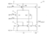
集積回路は、メモリ等のデジタル回路と、図1に示す2段増幅オペアンプ(以下、「オペアンプ1」)とを備える。オペアンプ1は、2つの入力電圧の差を増幅する回路であり、初段となる差動増幅段10と、最終段となる出力段20とを備える。オペアンプ1は、ひとつの半導体基板に一体集積化されている。オペアンプ1は、反転入力端子INNと非反転入力端子INPとの電位差を増幅し、出力端子OUTから電圧信号となる出力信号Soutを出力する。
(First Embodiment)
The integrated circuit includes a digital circuit such as a memory and a two-stage amplifier operational amplifier (hereinafter, “
差動増幅段10は、差動対11、テイル電流源12、及びカレントミラー回路13を含む。
差動対11は、第1トランジスタM1及び第2トランジスタM2を含む。本実施形態では、第1トランジスタM1及び第2トランジスタM2は、NチャネルMOSFETである。第1トランジスタM1及び第2トランジスタM2は、デプレッション型及びエンハンスメント型のいずれかの構造を取り得る。本実施形態では、第1トランジスタM1及び第2トランジスタM2は、エンハンスメント型の構造である。第1トランジスタM1のゲートは非反転入力端子INPと接続され、第2トランジスタM2のゲートは反転入力端子INNと接続される。第1トランジスタM1のソース及び第2トランジスタM2のソースは共通に接続されている。差動対11は、反転入力端子INN及び非反転入力端子INPのそれぞれの入力電圧Vinn,Vinpに応じた差動電流Im1,Im2を生成する。
The
The differential pair 11 includes a first transistor M1 and a second transistor M2. In this embodiment, the first transistor M1 and the second transistor M2 are N-channel MOSFETs. The first transistor M1 and the second transistor M2 may have either a depletion type structure or an enhancement type structure. In the present embodiment, the first transistor M1 and the second transistor M2 have an enhancement type structure. The gate of the first transistor M1 is connected to the non-inverting input terminal INP, and the gate of the second transistor M2 is connected to the inverting input terminal INN. The source of the first transistor M1 and the source of the second transistor M2 are commonly connected. The differential pair 11 generates differential currents Im1 and Im2 according to the input voltages Vinn and Vinp of the inverting input terminal INN and the non-inverting input terminal INP, respectively.
テイル電流源12は、各トランジスタM1,M2のソースに接続される第3トランジスタM3を含む。本実施形態の第3トランジスタM3は、NチャネルMOSFETである。第3トランジスタM3のソースは、第2の電源配線3に接続されて、第2の電源電圧VSSが印加される。第3トランジスタM3のゲートは、BIAS端子に接続されている。第3トランジスタM3のゲートには、バイアス回路(図示略)からのバイアス電圧Vbnが入力される。テイル電流源12は、バイアス電圧Vbnに基づいてテイル電流Itを供給する。
The tail
カレントミラー回路13は、差動対11と接続される能動負荷である。カレントミラー回路13は、第4トランジスタM4及び第5トランジスタM5を含む。第4トランジスタM4及び第5トランジスタM5は、エンハンスメント型のPチャネルMOSFETである。第4トランジスタM4のソース及び第5トランジスタM5のソースは、第1の電源配線2に接続されて、第1の電源電圧VDDが印加される。第4トランジスタM4のゲート及びドレインは、第1トランジスタM1のドレインに共通接続されている。第5トランジスタM5のゲートは第4トランジスタM4のゲートに接続され、第5トランジスタM5のドレインは第2トランジスタM2のドレインに接続されている。
The
出力段20は、第6トランジスタM6及び第7トランジスタM7を用いたソース接地回路である。第6トランジスタM6はPチャネルMOSFETであり、第7トランジスタM7はNチャネルMOSFETである。第6トランジスタM6のソースは第1の電源配線2に接続され、第6トランジスタM6のドレインは第7トランジスタM7のドレインに接続されている。第6トランジスタM6のゲートは、第5トランジスタM5と第2トランジスタM2との間のノードN1に接続されている。第7トランジスタM7のソースは第2の電源配線3に接続されている。第7トランジスタM7のゲートは、第3トランジスタM3のゲートと共通して接続され、BIAS端子に接続されている。第7トランジスタM7のゲートにはバイアス回路からのバイアス電圧Vbnが入力される。
The
このような各トランジスタM1〜M7においては、差動対11を構成する第1トランジスタM1及び第2トランジスタM2のゲート長は、カレントミラー回路13を構成する第4トランジスタM4及び第5トランジスタM5のゲート長よりも短い。このようなゲート長の関係により、差動増幅段10の移動度の揺らぎを低減できるため、出力信号Soutの1/fノイズを低減できる。
In each of the transistors M1 to M7, the gate lengths of the first transistor M1 and the second transistor M2 constituting the differential pair 11 are the gates of the fourth transistor M4 and the fifth transistor M5 constituting the
さらに、本実施形態では、オペアンプ1の出力信号Soutの1/fノイズの更なる低減のため、各トランジスタM1〜M7のうちの一部のトランジスタにおけるチャネル領域の不純物濃度を、各トランジスタM1〜M7のうちの他のトランジスタにおけるチャネル領域の不純物濃度よりも低くしている。すなわち、オペアンプ1の複数のトランジスタは、チャネル領域の不純物濃度が第1濃度である高濃度トランジスタと、チャネル領域の不純物濃度が第1濃度よりも低い第2濃度である低濃度トランジスタとを含む。具体的には、各トランジスタM1〜M7のうちの出力信号Soutの1/fノイズの影響を受け易いトランジスタにおけるチャネル領域の不純物濃度を、各トランジスタM1〜M7のうちの出力信号Soutの1/fノイズの影響を受け難いトランジスタにおけるチャネル領域の不純物濃度よりも低くしている。すなわち、低濃度トランジスタは、高濃度トランジスタよりも、複数のトランジスタのうちオペアンプ1の1/fノイズの影響を受け易いトランジスタに用いられ、高濃度トランジスタは、低濃度トランジスタよりも、複数のトランジスタのうちオペアンプ1の1/fノイズの影響を受け難いトランジスタに用いられている。詳細には、オペアンプ1において、出力信号Soutの1/fノイズの影響を受け易い部分は差動増幅段10の一部であり、出力信号Soutの1/fノイズの影響を受け難い部分は出力段20である。より詳細には、差動増幅段10において差動対11及びカレントミラー回路13が出力信号Soutの1/fノイズの影響を受け易く、テイル電流源12が出力信号Soutの1/fノイズの影響を受け難い。
Further, in the present embodiment, in order to further reduce the 1 / f noise of the output signal Sout of the
本実施形態では、差動増幅段10における差動対11及びカレントミラー回路13のトランジスタにおけるチャネル領域の不純物濃度を、テイル電流源12及び出力段20のトランジスタにおけるチャネル領域の不純物濃度よりも低くしている。すなわち、差動対11及びカレントミラー回路13を構成するトランジスタは、低濃度トランジスタであり、テイル電流源12及び出力段20を構成するトランジスタは、高濃度トランジスタである。具体的には、第1トランジスタM1、第2トランジスタM2、第4トランジスタM4、及び第5トランジスタM5におけるチャネル領域の不純物濃度を、第3トランジスタM3、第6トランジスタM6、及び第7トランジスタM7におけるチャネル領域の不純物濃度よりも低くしている。すなわち、第1トランジスタM1、第2トランジスタM2、第4トランジスタM4、及び第5トランジスタM5は低濃度トランジスタであり、第3トランジスタM3、第6トランジスタM6、及び第7トランジスタM7は高濃度トランジスタである。
In the present embodiment, the impurity concentration in the channel region of the transistors of the differential pair 11 and the
また、オペアンプ1は、各トランジスタM1〜M7が半導体プロセスの微細化技術によって製造されることにより、高い集積度を実現している。各トランジスタM1〜M7は、素子分離構造としてSTI(Shallow Trench Isolation)構造が用いられる。
Further, the
図2Aに示すように、NチャネルMOSFETである第3トランジスタM3は、半導体基板としてのP型のシリコン基板30上に成長させられたP型エピタキシャル層31に形成されている。P型エピタキシャル層31の表層部には、P型エピタキシャル層31を複数の領域に分離する浅いトレンチ32が形成されている。トレンチ32には、シリコン酸化膜33が埋め込まれている。トレンチ32(シリコン酸化膜33)の幅は、例えば0.22μmである。そして、P型エピタキシャル層31には、トレンチ32により分離(STI)されたアクティブ領域が形成されている。図2Aに示されるアクティブ領域は、第3トランジスタM3が形成される素子形成領域34である。一方、トレンチ32に対応する領域は、素子分離領域35である。素子分離領域35は、P型ウェル層36及びP型ドリフト層37を含む。P型ウェル層36は、トレンチ32の底部に隣接するように設けられている。P型ドリフト層37は、P型ウェル層36に対してシリコン基板30側にP型ウェル層36と隣接するように設けられている。これにより、より確実な素子分離が達成されている。さらに、素子分離領域35には、P型ドリフト層37に対してシリコン基板30側に深さ方向に間隔を空けてP型埋め込み層(LI)38が形成されている。P型埋め込み層38は、シリコン基板30とP型エピタキシャル層31との境界部に形成されている。
As shown in FIG. 2A, the third transistor M3, which is an N-channel MOSFET, is formed on a P-
素子形成領域34は、深いN型ウェル層39(HVNW)及びN型埋め込み層(BL)40を有する。N型ウェル層39は、高耐圧ウェル領域であり、素子分離領域35によって分離されている。N型埋め込み層40は、素子形成領域34においてN型ウェル層39に対してシリコン基板30側に深さ方向に間隔を空けて形成されている。N型埋め込み層40は、シリコン基板30とP型エピタキシャル層31との境界部に形成されている。
The
N型ウェル層39の表層部には、P型ウェル層41がN型ウェル層39に取り囲まれるように形成されている。P型ウェル層41は、P型不純物がドープされた領域である。P型不純物としては、例えばB(ホウ素)などを用いることができる。P型ウェル層41は、P型不純物濃度が例えば1E+17〜1E+18cm−3となるようにP型不純物がドープされた領域である。
A P-
P型ウェル層41の表面には、ゲート絶縁膜42が形成されている。ゲート絶縁膜42は、例えばシリコン酸化膜によって構成されている。ゲート絶縁膜42の厚さは、例えば、1〜20nmである。
A
ゲート絶縁膜42上には、ゲート電極43が形成されている。ゲート電極43は、例えば、Si,Co,Hf,Zr、Al、Ti、Ta、Moなどからなり、その合金も含む。また、ゲート電極43の厚さは、例えば、50〜250nmである。また、P型ウェル層41の表面には、ゲート電極43の側壁を全周に亘って取り囲むサイドウォール44が形成されている。サイドウォール44は、例えば、酸化シリコン、窒化シリコン、又はそれらの積層構造からなる。
A
P型ウェル層41には、ゲート絶縁膜42と対向する領域(チャネル領域)を含む一方側(図2Aにおける左側)および他方側(図2Aにおける右側)に、それぞれN型のソース領域45及びN型のドレイン領域46が形成されている。
The P-
本実施形態において第3トランジスタM3のチャネル領域は、P型ウェル層41のうちゲート絶縁膜42の下方であってソース領域45とドレイン領域46との間に配置されている。本実施形態において、第3トランジスタM3のチャネル領域は、P型ウェル層41とゲート絶縁膜42との界面を含む。なお、第3トランジスタM3のチャネル領域の不純物濃度は、P型ウェル層41の不純物濃度と同一である。
In the present embodiment, the channel region of the third transistor M3 is arranged below the
ソース領域45は、N型不純物が低濃度及び高濃度で二重拡散された構造をなしている。ソース領域45は、N型不純物が低濃度で拡散されたN−型の低濃度ソース領域47と、N型不純物が高濃度で拡散されたN+型の高濃度ソース領域48とを有する。
The
低濃度ソース領域47は、N型不純物濃度が例えば5E+17〜5E+18cm−3となるようにN型不純物がドープされた領域であり、P型ウェル層41の表面からその深さ方向に広がり、その一部がゲート絶縁膜42の幅方向の一方側縁部に対向するように形成されている。低濃度ソース領域47の深さは、例えば100〜400nmである。
The low-
高濃度ソース領域48は、N型不純物濃度が例えば5E+19〜5E+20cm−3となるようにN型不純物がドープされた領域であり、P型ウェル層41の表面からその深さ方向に広がり、サイドウォール44に対して自己整合的に形成されている。高濃度ソース領域48の深さは、例えば50〜200nmである。
The high-
ドレイン領域46は、N型不純濃度が低濃度及び高濃度で二重拡散された構造をなしている。ドレイン領域46は、N型不純物が低濃度で拡散されたN−型の低濃度ドレイン領域49と、N型不純物が高濃度で拡散されたN+型の高濃度ドレイン領域50とを有する。
The
低濃度ドレイン領域49は、N型不純物濃度が例えば5E+17〜5E+18cm−3となるようにN型不純物がドープされた領域であり、P型ウェル層41の表面からその深さ方向に広がり、その一部がゲート絶縁膜42の幅方向の他方側縁部に対向するように形成されている。低濃度ドレイン領域49の深さは、例えば低濃度ソース領域47の深さと同じである。
The low-
高濃度ドレイン領域50は、N型不純物濃度が例えば5E+19〜5E+20cm−3となるようにN型不純物がドープされた領域であり、P型ウェル層41の表面からその深さ方向に広がり、サイドウォール44に対して自己整合的に形成されている。高濃度ドレイン領域50の深さは、高濃度ソース領域48の深さと同じである。
The high-
シリコン基板30上には、絶縁膜としての第1絶縁層51及び第2絶縁層52がこの順に積層されている。
第1絶縁層51は、P型エピタキシャル層31の表面及びサイドウォール44の側面に形成された膜53と、膜53上に形成された第1層間絶縁膜54とを有する。膜53は、例えば窒化シリコン(SiN)からなる。第1層間絶縁膜54は、例えば酸化シリコン(SiO2)からなる。膜53の厚さは例えば10〜100nmであり、第1層間絶縁膜54の厚さは例えば300〜500nmである。
The first insulating
The first insulating
第2絶縁層52は、酸化シリコン(SiO2)からなる単層膜である。第2絶縁層52の厚さは、例えば100〜300nmである。
第1絶縁層51及び第2絶縁層52においてソース領域45及びドレイン領域46に対向する部分には、これらを連続して貫通するソースコンタクトホール55及びドレインコンタクトホール56が形成されている。
The second insulating
Source contact holes 55 and drain contact holes 56 that continuously penetrate the
ソースコンタクトホール55には、ソースコンタクトプラグ57が埋設されている。ソースコンタクトプラグ57は、W/TiN/Tiの積層構造からなり、ソース領域45に接触(コンタクト)している。そして第2絶縁層52上には、ソースコンタクトプラグ57と一体をなす、Al/TiN/Tiの積層構造からなるソース配線58が形成されている。
A
ドレインコンタクトホール56には、ドレインコンタクトプラグ59が埋設されている。ドレインコンタクトプラグ59は、アルミニウムからなり、ドレイン領域46に接触(コンタクト)している。そして第2絶縁層52上には、ドレインコンタクトプラグ59と一体をなす、アルミニウムからなるドレイン配線60が形成されている。またゲート電極43には、ゲート配線61が接続されている。なお、第7トランジスタM7も第3トランジスタM3と同様の構成である。
A
図2Bに示すように、NチャネルMOSFETである第1トランジスタM1は、第3トランジスタM3と同様に、P型エピタキシャル層31の表層部に形成されている。図2Bに示されるP型エピタキシャル層31においてトレンチ32により分離(STI)されたアクティブ領域は、第1トランジスタM1が形成される素子形成領域34である。第1トランジスタM1は、P型ウェル層の不純物濃度以外は、第3トランジスタM3と同一構造である。
As shown in FIG. 2B, the first transistor M1 which is an N-channel MOSFET is formed on the surface layer portion of the P-
第1トランジスタM1のP型ウェル層62は、P型エピタキシャル層31において第1トランジスタM1が形成される素子形成領域34に形成されている。P型ウェル層62の深さ及び幅は、第3トランジスタM3のP型ウェル層41の深さ及び幅と概ね同じである。一方、P型ウェル層62のP型不純物濃度は、第3トランジスタM3のP型ウェル層41のP型不純物濃度よりも低い。詳細には、第3トランジスタM3のP型ウェル層41のP型不純物濃度は、スケーリング則(比例縮小則)に沿ったP型不純物濃度である。第1トランジスタM1のP型ウェル層62のP型不純物濃度は、スケーリング則に沿ったP型不純物濃度よりも低い。P型ウェル層62のP型不純物濃度は、P型不純物濃度の低下に起因して素子特性が過度にずれない範囲で極力低いことが好ましい。一例では、P型ウェル層62のP型不純物濃度は、第3トランジスタM3のP型ウェル層41のP型不純物濃度の約1/2以下である。好ましくは、P型ウェル層62のP型不純物濃度は、第3トランジスタM3のP型ウェル層41のP型不純物濃度の約1/10である。本実施形態のP型ウェル層62のP型不純物濃度は、1E+16〜1E+17cm−3である。
The P-
本実施形態において第1トランジスタM1のチャネル領域は、P型ウェル層62のうちゲート絶縁膜42の下方であってソース領域45とドレイン領域46との間に配置されている。本実施形態において、第1トランジスタM1のチャネル領域は、P型ウェル層62とゲート絶縁膜42との界面を含む。なお、第1トランジスタM1のチャネル領域の不純物濃度は、P型ウェル層62の不純物濃度と同一である。また、第2トランジスタM2は、第1トランジスタM1と同様の構成である。
In the present embodiment, the channel region of the first transistor M1 is arranged below the
図2Cに示すように、PチャネルMOSFETである第6トランジスタM6は、第3トランジスタM3と同様に、P型エピタキシャル層31の表層部に形成されている。図2Cに示されるP型エピタキシャル層31においてトレンチ32により分離(STI)されたアクティブ領域は、第6トランジスタM6が形成される素子形成領域34である。
As shown in FIG. 2C, the sixth transistor M6, which is a P-channel MOSFET, is formed on the surface layer portion of the P-
素子形成領域34には、N型ウェル層63を有する。N型ウェル層63は、N型ウェル層39の表層部においてN型ウェル層39に取り囲まれるように形成されている。N型ウェル層63は、N型不純物がドープされた領域である。N型不純物としては、例えばP(リン)などを用いることができる。N型ウェル層63は、N型不純物濃度が例えば1E+17〜1E+18cm−3となるようにN型不純物がドープされた領域である。
The
N型ウェル層63の表面には、第3トランジスタM3と同様に、ゲート絶縁膜42が形成され、ゲート絶縁膜42上には、ゲート電極43が形成されている。ゲート絶縁膜42及びゲート電極43の材料及び厚さは、第3トランジスタM3のゲート絶縁膜42及びゲート電極43と同じである。また、N型ウェル層63の表面には、ゲート電極43の側壁を全周に亘って取り囲むサイドウォール44が形成されている。サイドウォール44は、例えば、酸化シリコンからなる。
Similar to the third transistor M3, a
N型ウェル層63には、ゲート絶縁膜42と対向する領域(チャネル領域)を含む一方側(図2Cにおける左側)および他方側(図2Cにおける右側)に、それぞれP型のソース領域64及びP型のドレイン領域65が形成されている。
The N-
本実施形態において第6トランジスタM6のチャネル領域は、N型ウェル層63のうちゲート絶縁膜42の下方であってソース領域64とドレイン領域65との間に配置されている。本実施形態において、第6トランジスタM6のチャネル領域は、N型ウェル層63とゲート絶縁膜42との界面を含む。なお、第6トランジスタM6のチャネル領域の不純物濃度は、N型ウェル層63の不純物濃度と同一である。
In the present embodiment, the channel region of the sixth transistor M6 is arranged below the
ソース領域64は、P型不純濃度が低濃度及び高濃度で二重拡散された構造をなしている。具体的には、P型不純物が低濃度で拡散されたP−型の低濃度ソース領域66と、P型不純物が高濃度で拡散されたP+型の高濃度ソース領域67とを有する。
The
低濃度ソース領域66は、P型不純物濃度が例えば5E+17〜5E+18cm−3となるようにP型不純物がドープされた領域であり、N型ウェル層63の表面からその深さ方向に広がり、その一部がゲート絶縁膜42の幅方向の一方側縁部に対向するように形成されている。低濃度ソース領域66の深さは、例えば50〜300nmである。
The low-
高濃度ソース領域67は、P型不純物濃度が例えば1E+19〜1E+20cm−3となるようにP型不純物がドープされた領域であり、N型ウェル層63の表面からその深さ方向に広がり、サイドウォール44に対して自己整合的に形成されている。高濃度ソース領域67の深さは、例えば50〜150nmである。
The high-
ドレイン領域65は、P型不純濃度が低濃度及び高濃度で二重拡散された構造をなしている。ドレイン領域65は、P型不純物が低濃度で拡散されたP−型の低濃度ドレイン領域68と、P型不純物が高濃度で拡散されたP+型の高濃度ドレイン領域69とを有する。
The
低濃度ドレイン領域68は、P型不純物濃度が例えば5E+17〜5E+18cm−3となるようにP型不純物がドープされた領域であり、N型ウェル層63の表面からその深さ方向に広がり、その一部がゲート絶縁膜42の幅方向の他方側縁部に対向するように形成されている。低濃度ドレイン領域68の深さは、例えば低濃度ソース領域66の深さと同じである。
The low-
高濃度ドレイン領域69は、P型不純物濃度が例えば1E+19〜1E+20cm−3となるようにP型不純物がドープされた領域であり、N型ウェル層63の表面からその深さ方向に広がり、サイドウォール44に対して自己整合的に形成されている。高濃度ドレイン領域69の深さは、高濃度ソース領域67の深さと同じである。
The high-
P型エピタキシャル層31上には、絶縁膜としての第1絶縁層51及び第2絶縁層52がこの順に積層されている。第1絶縁層51及び第2絶縁層52には、ソースコンタクトホール55及びドレインコンタクトホール56が形成され、ソースコンタクトプラグ57及びドレインコンタクトプラグ59がそれぞれ埋設されている。第6トランジスタM6の第1絶縁層51、第2絶縁層52、ソースコンタクトホール55、ドレインコンタクトホール56、ソースコンタクトプラグ57、及びドレインコンタクトプラグ59は、第3トランジスタM3の第1絶縁層51、第2絶縁層52、ソースコンタクトホール55、ドレインコンタクトホール56、ソースコンタクトプラグ57、及びドレインコンタクトプラグ59と同じ構造である。
A first insulating
図2Dに示すように、PチャネルMOSFETである第4トランジスタM4は、第6トランジスタM6と同様に、P型エピタキシャル層31の表層部に形成されている。第4トランジスタM4は、N型ウェル層の不純物濃度以外は、第6トランジスタM6と同一構造である。
As shown in FIG. 2D, the fourth transistor M4, which is a P-channel MOSFET, is formed on the surface layer portion of the P-
第4トランジスタM4のN型ウェル層70は、P型エピタキシャル層31において第4トランジスタM4が形成される素子形成領域34に形成されている。N型ウェル層70の深さ及び幅は、第6トランジスタM6のN型ウェル層63の深さ及び幅と概ね同じである。一方、N型ウェル層70のN型不純物濃度は、第6トランジスタM6のN型ウェル層63のN型不純物濃度よりも低い。詳細には、第6トランジスタM6のN型ウェル層63のN型不純物濃度は、スケーリング則(比例縮小則)に沿ったN型不純物濃度である。第4トランジスタM4のN型ウェル層70のN型不純物濃度は、スケーリング則に沿ったN型不純物濃度よりも低い。N型ウェル層70のN型不純物濃度は、N型不純物濃度の低下に起因して素子特性が過度にずれない範囲で極力低いことが好ましい。素子特性が過度にずれない範囲とは、例えばしきい値電圧がずれてカレントミラー回路13の機能が成り立たなくなってしまうN型不純物濃度の上限値よりも高い濃度である。一例では、N型ウェル層70のN型不純物濃度は、第6トランジスタM6のN型ウェル層63のN型不純物濃度の約1/2以下である。好ましくは、N型ウェル層70のN型不純物濃度は、第6トランジスタM6のN型ウェル層63のN型不純物濃度の約1/10である。本実施形態のN型ウェル層70のP型不純物濃度は、1E+16〜1E+17cm−3である。
The N-
本実施形態において第4トランジスタM4のチャネル領域は、N型ウェル層70のうちゲート絶縁膜42の下方であってソース領域64とドレイン領域65との間に配置されている。本実施形態において、第4トランジスタM4のチャネル領域は、N型ウェル層70とゲート絶縁膜42との界面を含む。なお、第4トランジスタM4のチャネル領域の不純物濃度は、N型ウェル層70の不純物濃度と同一である。また、第5トランジスタM5は、第4トランジスタM4と同一構造である。
In the present embodiment, the channel region of the fourth transistor M4 is arranged below the
〔トランジスタの製造方法〕
図3A〜図3Mを参照して、第1トランジスタM1、第3トランジスタM3、第4トランジスタM4、及び第6トランジスタM6の製造方法について説明する。なお、図3A〜図3Mでは、説明の便宜上、第1トランジスタM1、第3トランジスタM3、第4トランジスタM4、及び第6トランジスタM6が隣り合うように形成されたと仮定している。
[Transistor manufacturing method]
A method for manufacturing the first transistor M1, the third transistor M3, the fourth transistor M4, and the sixth transistor M6 will be described with reference to FIGS. 3A to 3M. In FIGS. 3A to 3M, for convenience of explanation, it is assumed that the first transistor M1, the third transistor M3, the fourth transistor M4, and the sixth transistor M6 are formed so as to be adjacent to each other.
これらトランジスタの製造方法は、エピタキシャル層形成工程(図3A)、アイソレーション形成工程(図3B及び図3C)、ウェル形成工程(図3D〜図3G)、ゲート形成工程(図3H及び図3I)、ソース・ドレイン形成工程(図3J〜図3L)、及び配線工程(図3M)を有する。 Methods for manufacturing these transistors include an epitaxial layer forming step (FIG. 3A), an isolation forming step (FIGS. 3B and 3C), a well forming step (FIGS. 3D to 3G), and a gate forming step (FIGS. 3H and 3I). It has a source / drain forming step (FIGS. 3J to 3L) and a wiring step (FIG. 3M).
図3Aに示すように、P型のシリコン基板30が準備され、例えば熱酸化法によって、シリコン基板30の表面上に熱酸化膜71が形成される。次に、シリコン基板30の表面に対して、N型埋め込み層40のためのイオン注入が行われる。例えば、N型不純物イオンとして砒素イオンが注入される。その後、注入したイオンを活性化するためのドライブ処理(熱処理)が実行される。次に、P型埋め込み層38のためのイオン注入が行われる。例えば、P型不純物イオンとしてボロンが注入される。
As shown in FIG. 3A, a P-
そしてシリコン基板30上にP型エピタキシャル層31が成長させられる。具体的には、P型不純物(例えばボロン)を添加しながら、シリコン結晶がエピタキシャル成長させられる。P型エピタキシャル層31の厚さは例えば5μm程度とされる。このエピタキシャル成長の際の熱によって、シリコン基板30に注入されたN型不純物及びP型不純物がシリコン基板30及びP型エピタキシャル層31内に拡散する。これにより、シリコン基板30とP型エピタキシャル層31との境界部にP型埋め込み層38及びN型埋め込み層40が形成される。
Then, the P-
図3Bに示すように、例えばCVD(Chemical Vapor Deposition:化学気相成長)法により、熱酸化膜71の全域を被覆するように窒化膜72が形成され、例えばフォトリソグラフィ及びエッチングにより、窒化膜72及び熱酸化膜71にトレンチ32を形成すべき領域を露出させる開口73が選択的に形成される。次に、窒化膜72及び熱酸化膜71をマスクとするエッチングにより、P型エピタキシャル層31の不要な部分が除去されてトレンチ32が形成される。次に、例えば熱酸化法によって、トレンチ32の側面及び底面に薄いライナー酸化膜(図示略)が形成される。次に、例えばCVD法によって、トレンチ32を埋めて窒化膜72の全域を被覆するように酸化シリコンからなる絶縁膜74(酸化シリコン膜)が形成される。
As shown in FIG. 3B, for example, a
次に、図3Cに示すように、トレンチ32に絶縁体となるシリコン酸化膜33が埋め込まれる。これにより、第1トランジスタM1、第3トランジスタM3、第4トランジスタM4、及び第6トランジスタM6を形成するための素子形成領域34を区画する素子分離領域35が形成される。そして、窒化膜72及び熱酸化膜71がエッチングによって順に除去される。
Next, as shown in FIG. 3C, a
図3Dに示すように、第1トランジスタM1、第3トランジスタM3、第4トランジスタM4、及び第6トランジスタM6を形成するための素子形成領域34のそれぞれには、高耐圧のN型ウェル層39が形成される。具体的には、素子形成領域34のそれぞれにN型不純物イオンが注入される。
As shown in FIG. 3D, a high withstand voltage N-
図3Eに示すように、素子分離領域35のそれぞれには、P型ドリフト層37が形成される。具体的には、素子分離領域35のそれぞれにP型不純物イオンが注入される。例えばP型不純物イオンとしてはボロンイオンが用いられる。その後、熱処理としてアニール処理が行われ、注入されたN型不純物イオン及びP型不純物イオンが活性化される。
As shown in FIG. 3E, a P-
図3Fに示すように、第3トランジスタM3に対応する素子形成領域34のN型ウェル層39の表層部にはP型ウェル層41が形成され、第6トランジスタM6に対応する素子形成領域34の表層部にはN型ウェル層63が形成される。つまり、図3Fに示すように、半導体基板であるシリコン基板30において第3トランジスタM3が形成される領域及び第6トランジスタM6が形成される領域にチャネル領域が形成される工程は、第2の工程となる。具体的には、第3トランジスタM3の素子形成領域34を露出させる開口を有するイオン注入マスク(図示略)が、第1トランジスタM1、第4トランジスタM4、及び第6トランジスタM6の素子形成領域34及び素子分離領域35を被覆するように形成される。そしてこのイオン注入マスクの開口を通じてP型不純物イオンが注入される。つまり、半導体基板であるシリコン基板30において第3トランジスタM3が形成される領域に不純物イオンが注入される一方、第1トランジスタM1、第4トランジスタM4、及び第6トランジスタM6が形成される領域に不純物イオンが注入されないように選択的にイオン注入を行うことにより、第3トランジスタM3が形成される領域にチャネル領域を形成する。例えばP型不純物イオンとしてはボロンイオンが用いられる。次に、第6トランジスタM6の素子形成領域34を露出させる開口を有するイオン注入マスク(図示略)が、第1トランジスタM1、第3トランジスタM3、及び第4トランジスタM4の素子形成領域34及び素子分離領域35を被覆するように形成される。そしてこのイオン注入マスクの開口を通じてN型不純物イオンが注入される。つまり、シリコン基板30において第6トランジスタM6が形成される領域に不純物イオンが注入される一方、第1トランジスタM1、第3トランジスタM3、及び第4トランジスタM4が形成される領域に不純物イオンが注入されないように選択的にイオン注入を行うことにより、第6トランジスタM6が形成される領域にチャネル領域を形成する。例えばN型不純物イオンとしては砒素イオン及びリンイオンが用いられる。なお、本実施形態では、第3トランジスタM3のP型ウェル層41が形成された後、第6トランジスタM6のN型ウェル層63が形成されたが、第6トランジスタM6のN型ウェル層63が形成された後、第3トランジスタM3のP型ウェル層41が形成されてもよい。
As shown in FIG. 3F, a P-
図3Gに示すように、第1トランジスタM1のN型ウェル層39の表層部にはP型ウェル層62が形成され、第4トランジスタM4のN型ウェル層39の表層部にはN型ウェル層70が形成される。つまり、図3Gに示すように、半導体基板であるシリコン基板30において第1トランジスタM1が形成される領域及び第4トランジスタM4が形成される領域にチャネル領域が形成される工程は、第1の工程となる。具体的には、第1トランジスタM1の素子形成領域34を露出させる開口を有するイオン注入マスク(図示略)が、第3トランジスタM3、第4トランジスタM4、及び第6トランジスタM6の素子形成領域34及び素子分離領域35を被覆するように形成される。そしてこのイオン注入マスクの開口を通じてP型不純物イオンが注入される。つまり、半導体基板であるシリコン基板30において第1トランジスタM1が形成される領域に不純物イオンが注入される一方、第3トランジスタM3、第4トランジスタM4、及び第6トランジスタM6が形成される領域に不純物イオンが注入されないように選択的にイオン注入を行うことにより、第3トランジスタM3が形成される領域にチャネル領域を形成する。例えばP型不純物イオンとしてはボロンイオンが用いられる。ここで、第1トランジスタM1のP型ウェル層41のP型不純物濃度が、第3トランジスタM3のP型ウェル層41のP型不純物濃度よりも低くなるようにイオン注入を行う。例えば、第1トランジスタM1のP型ウェル層62のP型不純物濃度が、第3トランジスタM3のP型ウェル層41のP型不純物濃度の約1/2程度となるようにイオン注入を行う。好ましくは、第1トランジスタM1のP型ウェル層62のP型不純物濃度が、第3トランジスタM3のP型ウェル層41のP型不純物濃度の約1/10となるようにイオン注入を行う。
As shown in FIG. 3G, a P-
次に、第4トランジスタM4の素子形成領域34を露出させる開口を有するイオン注入マスク(図示略)が、第1トランジスタM1、第3トランジスタM3、及び第6トランジスタM6の素子形成領域34及び素子分離領域35を被覆するように形成される。そしてこのイオン注入マスクの開口を通じてN型不純物イオンが注入される。つまり、半導体基板であるシリコン基板30において第4トランジスタM4が形成される領域に不純物イオンが注入される一方、第1トランジスタM1、第3トランジスタM3、及び第6トランジスタM6が形成される領域に不純物イオンが注入されないように選択的にイオン注入を行うことにより、第4トランジスタM4が形成される領域にチャネル領域を形成する。例えばN型不純物イオンとしては砒素イオン及びリンイオンが用いられる。ここで、第4トランジスタM4のN型ウェル層70のN型不純物濃度が、第6トランジスタM6のN型ウェル層63のN型不純物濃度よりも低くなるようにイオン注入を行う。例えば、第4トランジスタM4のN型ウェル層70のN型不純物濃度が、第6トランジスタM6のN型ウェル層63のN型不純物濃度の約1/2以下となるようにイオン注入を行う。好ましくは、第4トランジスタM4のN型ウェル層70のN型不純物濃度が、第6トランジスタM6のN型ウェル層63のN型不純物濃度の約1/10となるようにイオン注入を行う。なお、本実施形態では、第1トランジスタM1のP型ウェル層62が形成された後、第4トランジスタM4のN型ウェル層70が形成されたが、第4トランジスタM4のN型ウェル層70が形成された後、第1トランジスタM1のP型ウェル層62が形成されてもよい。つまり、本実施形態では、第2の工程の後に第1の工程が行われたが、第1の工程の後に第2の工程を行ってもよい。
Next, an ion implantation mask (not shown) having an opening that exposes the
図3Hに示すように、P型エピタキシャル層31の各素子形成領域34における表面には、例えば熱酸化法によって熱酸化膜75が形成される。次に、熱酸化膜75及びシリコン酸化膜33を被覆するようにポリシリコン膜76が形成される。
As shown in FIG. 3H, a
図3Iに示すように、例えばフォトリソグラフィ及びエッチングにより、第1トランジスタM1、第3トランジスタM3、第4トランジスタM4、及び第6トランジスタM6の素子形成領域34には、熱酸化膜75及びポリシリコン膜76の不要な部分が除去されて所定の形状にパターニングされたゲート絶縁膜42及びゲート電極43が形成される。そして、例えばCVD法によりP型エピタキシャル層31上に窒化膜/酸化膜の積層膜(図示略)が形成された後、選択的にエッチングされて各ゲート電極43の側面にサイドウォール44が形成される。
As shown in FIG. 3I, for example, by photolithography and etching, a
図3Jに示すように、第1トランジスタM1及び第3トランジスタM3の素子形成領域34に低濃度ソース領域47及び低濃度ドレイン領域49が形成され、第4トランジスタM4及び第6トランジスタM6の素子形成領域34に低濃度ソース領域66及び低濃度ドレイン領域68が形成される。具体的には、第1トランジスタM1及び第3トランジスタM3の素子形成領域34を露出させる開口を有するイオン注入マスク(図示略)が、第4トランジスタM4及び第6トランジスタM6の素子形成領域34及び素子分離領域35を被覆するように形成される。そしてこのイオン注入マスクの開口を通じてN型不純物イオンが注入される。次に、上記イオン注入マスクを除去し、第4トランジスタM4及び第6トランジスタM6の素子形成領域34を露出させる開口を有するイオン注入マスク(図示略)が、第1トランジスタM1及び第3トランジスタM3の素子形成領域34及び素子分離領域35を被覆するように形成される。そしてこのイオン注入マスクの開口を通じてP型不純物イオンが注入される。例えば、P型不純物イオンとしてはBF2イオンが用いられる。なお、本実施形態では、低濃度ソース領域47及び低濃度ドレイン領域49が形成された後、低濃度ソース領域66及び低濃度ドレイン領域68が形成されたが、低濃度ソース領域66及び低濃度ドレイン領域68が形成された後、低濃度ソース領域47及び低濃度ドレイン領域49が形成されてもよい。
As shown in FIG. 3J, a low-
図3Kに示すように、第1トランジスタM1及び第3トランジスタM3の素子形成領域34に高濃度ソース領域48及び高濃度ドレイン領域50が形成され、第4トランジスタM4及び第6トランジスタM6の素子形成領域34に高濃度ソース領域67及び高濃度ドレイン領域69が形成される。具体的には、第1トランジスタM1及び第3トランジスタM3の素子形成領域34を露出させる開口を有するイオン注入マスク(図示略)が、第4トランジスタM4及び第6トランジスタM6の素子形成領域34及び素子分離領域35を被覆するように形成される。そしてこのイオン注入マスクの開口を通じてN型不純物イオンが注入される。次に、上記イオン注入マスクを除去し、第4トランジスタM4及び第6トランジスタM6の素子形成領域34を露出させる開口を有するイオン注入マスク(図示略)が、第1トランジスタM1及び第3トランジスタM3の素子形成領域34及び素子分離領域35を被覆するように形成される。そしてこのイオン注入マスクの開口を通じてP型不純物イオンが注入される。例えば、P型不純物イオンとしてはボロンイオンが用いられる。なお、本実施形態では、高濃度ソース領域48及び高濃度ドレイン領域50が形成された後、高濃度ソース領域67及び高濃度ドレイン領域69が形成されたが、高濃度ソース領域67及び高濃度ドレイン領域69が形成された後、高濃度ソース領域48及び高濃度ドレイン領域50が形成されてもよい。
As shown in FIG. 3K, a high-
図3Lに示すように、第1トランジスタM1及び第3トランジスタM3の素子形成領域34に形成された高濃度ソース領域48、高濃度ドレイン領域50、及びゲート電極43の表面にシリサイド層77が形成される。また第4トランジスタM4及び第6トランジスタM6の素子形成領域34に形成された高濃度ソース領域67、高濃度ドレイン領域69、及びゲート電極43の表面にシリサイド層77が形成される。具体的には、P型エピタキシャル層31の表面に例えばPVD法によってコバルト膜(図示略)が形成された後、加熱処理が行われる。これにより、各素子形成領域34における高濃度ソース領域48、67、高濃度ドレイン領域50、69、及びゲート電極43のコバルト膜がシリサイド層77に変化する一方、各素子分離領域35におけるシリコン酸化膜33上のコバルト膜はコバルトのままとなる。そして、例えば薬液処理によって各シリコン酸化膜33上のコバルトが選択的に除去される。
As shown in FIG. 3L, the
図3Mに示すように、第1絶縁層51、第2絶縁層52、ソース配線58、及びドレイン配線60が形成される。具体的には、例えばCVD法によってP型エピタキシャル層31上に窒化膜及び酸化膜が連続して積層されて膜53及び第1層間絶縁膜54が形成される。そして例えばCMP処理によって第1層間絶縁膜54が研磨される。次に、第1層間絶縁膜54上に酸化シリコン膜としての第2絶縁層52が積層するように形成される。次に、フォトリソグラフィ及びエッチングによって各素子形成領域34には、第2絶縁層52及び第1絶縁層51にソースコンタクトホール55及びドレインコンタクトホール56が形成され、ソースコンタクトプラグ57、ドレインコンタクトプラグ59、ソース配線58、及びドレイン配線60の材料であるTi/TiN/Alが第2絶縁層52上に堆積される。そしてフォトリソグラフィ及びエッチングによってTi/TiN/Al積層膜がパターニングされてソースコンタクトプラグ57、ドレインコンタクトプラグ59、ソース配線58、及びドレイン配線60が形成される。またゲート配線61(図3Mでは図示略)が形成される。以上により、第1トランジスタM1、第3トランジスタM3、第4トランジスタM4、及び第6トランジスタM6が製造される。
As shown in FIG. 3M, the first insulating
なお、第2トランジスタM2は第1トランジスタM1と同様に製造され、第5トランジスタM5は第4トランジスタM4と同様に製造され、第7トランジスタM7は第3トランジスタM3と同様に製造される。また、第1トランジスタM1と第2トランジスタM2とは同時に形成され、第4トランジスタM4と第5トランジスタM5とは同時に形成され、第3トランジスタM3と第7トランジスタM7とは同時に形成される。 The second transistor M2 is manufactured in the same manner as the first transistor M1, the fifth transistor M5 is manufactured in the same manner as the fourth transistor M4, and the seventh transistor M7 is manufactured in the same manner as the third transistor M3. Further, the first transistor M1 and the second transistor M2 are formed at the same time, the fourth transistor M4 and the fifth transistor M5 are formed at the same time, and the third transistor M3 and the seventh transistor M7 are formed at the same time.
図4A,図4B,図5を参照して、本実施形態の作用及び効果について説明する。なお、図4A及び図4Bは、ゲート電極43とチャネル領域との界面における原子配列を模式的に示す図であり、図4Aは、チャネル領域の不純物濃度が低い場合の電子の動きの一例を示し、図4Bは、チャネル領域の不純物濃度が高い場合の電子の動きの一例を示す。言い換えれば、図4Bは、チャネル領域の不純物濃度が第1濃度である高濃度トランジスタのチャネル領域の電子の動きの一例を示し、図4Aは、チャネル領域の不純物濃度が第1濃度よりも低い第2濃度である低濃度トランジスタのチャネル領域の電子の動きの一例を示している。なお、図4A及び図4Bにおける網掛けの円は不純物である。
The operation and effect of this embodiment will be described with reference to FIGS. 4A, 4B, and 5. 4A and 4B are diagrams schematically showing the atomic arrangement at the interface between the
集積回路のロジック集積度の向上のため、トランジスタの微細化が行われている。例えば、各トランジスタM1〜M7の最小寸法のサイズは、0.05〜10μmであると好ましく、本実施形態では例えば0.13μmである。このようなトランジスタの微細化に伴い、集積回路の出力信号の1/fノイズ(フリッカノイズ)が大きくなる場合がある。 Transistors have been miniaturized in order to improve the degree of logic integration of integrated circuits. For example, the size of the minimum dimension of each transistor M1 to M7 is preferably 0.05 to 10 μm, and in this embodiment, for example, 0.13 μm. With the miniaturization of such transistors, 1 / f noise (flicker noise) of the output signal of the integrated circuit may increase.
本願発明者らは、出力信号の1/fノイズがドレイン電流の揺らぎに起因し、当該ドレイン電流の揺らぎはトランジスタの移動度の揺らぎに起因していることに着目した。また、上記移動度の揺らぎの一因として、チャネル領域の不純物濃度に着目した。 The inventors of the present application have noted that the 1 / f noise of the output signal is caused by the fluctuation of the drain current, and the fluctuation of the drain current is caused by the fluctuation of the mobility of the transistor. In addition, we focused on the impurity concentration in the channel region as one of the causes of the fluctuation of the mobility.
詳述すると、図4A及び図4Bに示すように、電子は不純物との散乱を受けながら、移動するため、チャネル領域の不純物濃度が高い場合の電子の移動軌跡(図4Bの矢印)は、チャネル領域の不純物濃度が低い場合の電子の移動軌跡(図4Aの矢印)よりも複雑になる。このため、チャネル領域の不純物濃度が高い場合の移動度の揺らぎは、チャネル領域の不純物濃度が低い場合の移動度の揺らぎよりも大きくなる。 More specifically, as shown in FIGS. 4A and 4B, the electrons move while being scattered with impurities, so that the electron movement locus (arrow in FIG. 4B) when the impurity concentration in the channel region is high is the channel. It is more complicated than the electron movement locus (arrow in FIG. 4A) when the impurity concentration in the region is low. Therefore, the mobility fluctuation when the impurity concentration in the channel region is high is larger than the mobility fluctuation when the impurity concentration in the channel region is low.
特に、通常、トランジスタの微細化を行う場合には、各トランジスタのショートチャネル効果を抑制するため、スケーリング則に基づいてチャネル領域の不純物濃度を高くすることが想定される。すると、不純物との散乱が生じ易く、移動度の揺らぎが大きくなり易い。 In particular, usually, when miniaturizing a transistor, it is assumed that the impurity concentration in the channel region is increased based on the scaling law in order to suppress the short channel effect of each transistor. Then, scattering with impurities is likely to occur, and the mobility fluctuation is likely to be large.
そこで、本願発明者らは、集積回路を構成する複数のトランジスタのうちの一部のトランジスタにおけるチャネル領域の不純物濃度を、他のトランジスタにおけるチャネル領域の不純物濃度よりも低くすることにより、移動度の揺らぎを小さくすることを知見した。すなわち本願発明者らは、集積回路の複数のトランジスタが、チャネル領域の不純物濃度が第1濃度である高濃度トランジスタと、チャネル領域の不純物濃度が第1濃度よりも低い第2濃度である低濃度トランジスタとを含むことにより、移動度の揺らぎを小さくすることを知見した。 Therefore, the inventors of the present application set the impurity concentration in the channel region of some of the plurality of transistors constituting the integrated circuit lower than the impurity concentration in the channel region of the other transistors to reduce the mobility. It was found that the fluctuation is reduced. That is, the inventors of the present application have a plurality of transistors in an integrated circuit having a high concentration transistor in which the impurity concentration in the channel region is the first concentration and a low concentration in which the impurity concentration in the channel region is a second concentration lower than the first concentration. It was found that the fluctuation of mobility can be reduced by including a transistor.
また、本実施形態では、各トランジスタM1〜M7のうちのオペアンプ1の出力信号Soutの1/fノイズの影響を受け難い第3トランジスタM3、第6トランジスタM6、及び第7トランジスタM7のP型ウェル層41及びN型ウェル層63の不純物濃度を比較的高くした。一方、本実施形態では、各トランジスタM1〜M7のうちのオペアンプ1の出力信号Soutの1/fノイズの影響を受け易い第1トランジスタM1、第2トランジスタM2、第4トランジスタM4、及び第5トランジスタM5のP型ウェル層62及びN型ウェル層70の不純物濃度をスケーリング則に拠らず、比較的低い不純物濃度にした。具体的には、第1トランジスタM1、第2トランジスタM2、第4トランジスタM4、及び第5トランジスタM5のP型ウェル層62及びN型ウェル層70の不純物濃度(第2濃度)を、第3トランジスタM3、第6トランジスタM6、及び第7トランジスタM7のP型ウェル層41及びN型ウェル層63の不純物濃度(第1濃度)の約1/10とした。これにより、出力信号Soutの1/fノイズの影響を受け易いトランジスタの移動度の揺らぎが小さくなる。
Further, in the present embodiment, the P-type wells of the third transistor M3, the sixth transistor M6, and the seventh transistor M7, which are not easily affected by the 1 / f noise of the output signal Sout of the
図5の実線は、第1トランジスタM1、第2トランジスタM2、第4トランジスタM4、及び第5トランジスタM5のP型ウェル層62及びN型ウェル層70の不純物濃度が、第3トランジスタM3、第6トランジスタM6、及び第7トランジスタM7のP型ウェル層41及びN型ウェル層63の不純物濃度と等しい場合の入力換算雑音電圧を示している。図5の破線は、第1トランジスタM1、第2トランジスタM2、第4トランジスタM4、及び第5トランジスタM5のP型ウェル層62及びN型ウェル層70の不純物濃度が、第3トランジスタM3、第6トランジスタM6、及び第7トランジスタM7のP型ウェル層41及びN型ウェル層63の不純物濃度の約1/2の場合の入力換算雑音電圧を示している。図5の二点鎖線は、第1トランジスタM1、第2トランジスタM2、第4トランジスタM4、及び第5トランジスタM5のP型ウェル層62及びN型ウェル層70の不純物濃度が、第3トランジスタM3、第6トランジスタM6、及び第7トランジスタM7のP型ウェル層41及びN型ウェル層63の不純物濃度の約1/10の場合の入力換算雑音電圧を示している。図5に示すように、第1トランジスタM1、第2トランジスタM2、第4トランジスタM4、及び第5トランジスタM5のP型ウェル層62及びN型ウェル層70の不純物濃度が低くなるにつれて入力換算雑音電圧、すなわち出力信号Soutの1/fノイズが低減されることが分かる。
The solid line in FIG. 5 shows that the impurity concentrations of the P-
本実施形態によれば、以下の効果が得られる。
(1−1)オペアンプ1の差動対11を構成する第1トランジスタM1及び第2トランジスタM2のP型ウェル層62の不純物濃度がオペアンプ1の最終段としての出力段20を構成する第6トランジスタM6のN型ウェル層63の不純物濃度及び第7トランジスタM7のP型ウェル層41よりも低い。この構成によれば、オペアンプ1において出力信号Soutの1/fノイズの影響を受け易い差動対11を構成する各トランジスタM1,M2のP型ウェル層62の不純物濃度を低くすることにより、移動度の揺らぎを抑制でき、ドレイン電流の揺らぎを抑制できる。したがって、オペアンプ1の1/fノイズを効果的に低減できる。
According to this embodiment, the following effects can be obtained.
(1-1) The sixth transistor in which the impurity concentration of the P-
一方、オペアンプ1の駆動電流に寄与する最終段の第6トランジスタM6のN型ウェル層63の不純物濃度及び第7トランジスタM7のP型ウェル層41の不純物濃度を相対的に高くすることにより、各トランジスタM6,M7のしきい値の変動を抑制できる。これにより、オペアンプ1の動作の安定化を図ることができる。
On the other hand, by relatively increasing the impurity concentration of the N-
詳述すると、オペアンプ1に含まれる複数のトランジスタには、安定したしきい値が求められるものが含まれている。このような安定したしきい値が求められるトランジスタに対して各トランジスタM1,M2のような低濃度のトランジスタが用いられると、オペアンプ1の動作が不安定なものとなってしまう恐れがある。
More specifically, the plurality of transistors included in the
この点、本実施形態では、オペアンプ1内に、各トランジスタM1,M2のような低濃度のトランジスタと、各トランジスタM6,M7のような高濃度のトランジスタとの双方が存在していることにより、1/fノイズを効果的に低減しつつ、オペアンプ1の動作の安定化を図ることができる。
In this respect, in the present embodiment, both low-concentration transistors such as the transistors M1 and M2 and high-concentration transistors such as the transistors M6 and M7 are present in the
(1−2)オペアンプ1のカレントミラー回路13を構成する第4トランジスタM4及び第5トランジスタM5のN型ウェル層70の不純物濃度がオペアンプ1の最終段としての出力段20を構成する第6トランジスタM6のN型ウェル層63の不純物濃度及び第7トランジスタM7のP型ウェル層41よりも低い。この構成によれば、オペアンプ1において出力信号Soutの1/fノイズの影響を受け易いカレントミラー回路13を構成する各トランジスタM4,M5のN型ウェル層70の不純物濃度を低くすることにより、移動度の揺らぎを抑制でき、ドレイン電流の揺らぎを抑制できる。したがって、オペアンプ1の1/fノイズを効果的に低減できる。
(1-2) The impurity concentration of the N-
(1−3)テイル電流源12を構成する第3トランジスタM3と、出力段20を構成する第7トランジスタM7とは、同一導電型のMOSFET(NチャネルMOSFET)であり、第3トランジスタM3のP型ウェル層41と第7トランジスタM7のP型ウェル層41とが同じ不純物濃度である。この構成によれば、第3トランジスタM3のP型ウェル層41を形成する工程と、第7トランジスタM7のP型ウェル層41を形成する工程とを一括に行うことができるため、オペアンプ1を製造する工程を簡略化することができる。
(1-3) The third transistor M3 constituting the tail
なお、図1に示すオペアンプ1は、図6に示すオペアンプ1Aのように変更できる。オペアンプ1Aは、各トランジスタM1〜M7の種類が主に異なる。
差動対11の第1トランジスタM1及び第2トランジスタM2、並びにテイル電流源12の第3トランジスタM3は、PチャネルMOSFETである。第3トランジスタM3のソースは第1の電源配線2に接続され、第3トランジスタM3のドレインは第1トランジスタM1及び第2トランジスタM2のソースに接続されている。
The
The first transistor M1 and the second transistor M2 of the differential pair 11 and the third transistor M3 of the tail
カレントミラー回路13の第4トランジスタM4及び第5トランジスタM5は、NチャネルMOSFETである。第4トランジスタM4及び第5トランジスタM5のソースは、第2の電源配線3に接続され、第4トランジスタM4のドレインは第1トランジスタM1のドレインに接続され、第5トランジスタM5のドレインは第2トランジスタM2のドレインに接続されている。
The fourth transistor M4 and the fifth transistor M5 of the
出力段20の第6トランジスタM6はNチャネルMOSFETであり、第7トランジスタM7はPチャネルMOSFETである。第6トランジスタM6のソースは第2の電源配線3に接続され、第7トランジスタM7のソースは第1の電源配線2に接続されている。
The sixth transistor M6 of the
オペアンプ1Aにおいては、本実施形態のオペアンプ1と同様に、第1トランジスタM1、第2トランジスタM2、第4トランジスタM4、及び第5トランジスタM5のP型ウェル層62及びN型ウェル層70の不純物濃度を、第3トランジスタM3、第6トランジスタM6、及び第7トランジスタM7のP型ウェル層41及びN型ウェル層63の不純物濃度よりも低くしている。このような構成のオペアンプ1Aにおいても、本実施形態のオペアンプ1と同様の効果が得られる。
In the
(第2実施形態)
図1、及び図7A〜図9Bを参照して、第2実施形態のオペアンプ1について説明する。本実施形態のオペアンプ1は、第1実施形態のオペアンプ1に比べ、オペアンプ1の出力信号Soutの1/fノイズを低減するために工夫するトランジスタの構造が異なる。
(Second Embodiment)
The
図7Aに示すように、本実施形態の第1トランジスタM1は、埋め込みチャネル型に変更された点以外は、第1実施形態の第3トランジスタM3と同一構造である。すなわち本実施形態の第1トランジスタM1におけるP型ウェル層78のP型不純物濃度は、第1実施形態の第1トランジスタM1におけるP型ウェル層62(図2B参照)のP型不純物濃度とは異なり、第3トランジスタM3のP型ウェル層41(図2A参照)のP型不純物濃度と同じである。
As shown in FIG. 7A, the first transistor M1 of the present embodiment has the same structure as the third transistor M3 of the first embodiment except that it is changed to the embedded channel type. That is, the P-type impurity concentration of the P-
P型ウェル層78においてゲート絶縁膜42と対向する領域(チャネル領域)には、埋め込みチャネル層79が形成されている。埋め込みチャネル層79は、ソース領域45及びドレイン領域46と同じ導電型の領域(層)である。すなわち埋め込みチャネル層79は、N型不純物がドープされたソース領域45及びドレイン領域46と同じN型の領域(層)である。埋め込みチャネル層79は、P型ウェル層78の内部に形成されている。詳細には、埋め込みチャネル層79は、P型ウェル層78とゲート絶縁膜42との界面に対して下方に離間した位置に形成されている。
An embedded
このように、本実施形態において第1トランジスタM1のチャネル領域(埋め込みチャネル層79)は、P型ウェル層78のうちゲート絶縁膜42の下方であってソース領域45とドレイン領域46との間に配置されている。本実施形態において、第1トランジスタM1のチャネル領域(埋め込みチャネル層79)は、P型ウェル層78とゲート絶縁膜42との界面を含まない。なお、第1トランジスタM1のチャネル領域(埋め込みチャネル層79)の合計不純物濃度は、P型ウェル層78の不純物濃度よりも高い。また、第2トランジスタM2は、第1トランジスタM1と同様の構成である。
As described above, in the present embodiment, the channel region (embedded channel layer 79) of the first transistor M1 is below the
図7Bに示すように、第4トランジスタM4は、埋め込みチャネル型に変更された点以外は、第6トランジスタM6と同一構造である。すなわち本実施形態の第4トランジスタM4におけるN型ウェル層80のN型不純物濃度は、第1実施形態の第4トランジスタM4におけるN型ウェル層70(図2D参照)のN型不純物濃度とは異なり、第6トランジスタM6のN型ウェル層63(図2C参照)のN型不純物濃度と同じである。
As shown in FIG. 7B, the fourth transistor M4 has the same structure as the sixth transistor M6 except that it has been changed to the embedded channel type. That is, the N-type impurity concentration of the N-
N型ウェル層80においてゲート絶縁膜42と対向する領域(チャネル領域)には、埋め込みチャネル層81が形成されている。埋め込みチャネル層81は、ソース領域64及びドレイン領域65と同じ導電型の領域(層)である。すなわち埋め込みチャネル層81は、P型不純物がドープされたソース領域64及びドレイン領域65と同じP型の領域(層)である。埋め込みチャネル層81は、N型ウェル層80の内部に形成されている。詳細には、埋め込みチャネル層81は、N型ウェル層80とゲート絶縁膜42との界面に対して下方に離間した位置に形成されている。
An embedded
このように、本実施形態において第4トランジスタM4のチャネル領域(埋め込みチャネル層81)は、N型ウェル層80のうちゲート絶縁膜42の下方であってソース領域64とドレイン領域65との間に配置されている。本実施形態において、第4トランジスタM4のチャネル領域(埋め込みチャネル層81)は、N型ウェル層80とゲート絶縁膜42との界面を含まない。なお、第4トランジスタM4のチャネル領域(埋め込みチャネル層81)の合計不純物濃度は、N型ウェル層80の不純物濃度よりも高い。また、第5トランジスタM5は、第4トランジスタM4と同様の構成である。
As described above, in the present embodiment, the channel region (embedded channel layer 81) of the fourth transistor M4 is below the
〔トランジスタの製造方法〕
図8A及び図8Bを参照して、第1トランジスタM1、第3トランジスタM3、第4トランジスタM4、及び第6トランジスタM6の製造方法について説明する。なお、図8A及び図8Bでは、説明の便宜上、第1トランジスタM1、第3トランジスタM3、第4トランジスタM4、及び第6トランジスタM6が隣り合うように形成されたと仮定している。本実施形態のトランジスタの製造方法は、第1実施形態のトランジスタの製造方法に比べ、ウェル形成工程が異なる。以下の説明では、ウェル形成工程について主に説明する。
[Transistor manufacturing method]
A method for manufacturing the first transistor M1, the third transistor M3, the fourth transistor M4, and the sixth transistor M6 will be described with reference to FIGS. 8A and 8B. In FIGS. 8A and 8B, for convenience of explanation, it is assumed that the first transistor M1, the third transistor M3, the fourth transistor M4, and the sixth transistor M6 are formed so as to be adjacent to each other. The method for manufacturing a transistor of the present embodiment is different from the method for manufacturing a transistor of the first embodiment in a well forming step. In the following description, the well forming step will be mainly described.
ウェル形成工程において、P型エピタキシャル層31の素子形成領域34に高耐圧のN型ウェル層39を形成する工程、及びP型エピタキシャル層31の素子分離領域35にP型ドリフト層37を形成する工程は、第1実施形態と同様である。
In the well forming step, a step of forming a high withstand voltage N-
図8Aに示すように、第1トランジスタM1のN型ウェル層39の表層部にはP型ウェル層78が形成され、第3トランジスタM3のN型ウェル層39の表層部にはP型ウェル層41が形成される。第4トランジスタM4のN型ウェル層39の表層部にはN型ウェル層80が形成され、第6トランジスタM6のN型ウェル層39の表層部にはN型ウェル層63が形成される。具体的には、第1トランジスタM1及び第3トランジスタM3の素子形成領域34を露出させる開口を有するイオン注入マスク(図示略)が、第4トランジスタM4及び第6トランジスタM6の素子形成領域34及び素子分離領域35を被覆するように形成される。そしてこのイオン注入マスクの開口を通じてP型不純物イオンが注入される。例えばP型不純物イオンとしてはボロンイオンが用いられる。次に、上記イオン注入マスクを除去し、第4トランジスタM4及び第6トランジスタM6の素子形成領域34を露出させる開口を有するイオン注入マスク(図示略)が、第1トランジスタM1及び第3トランジスタM3の素子形成領域34及び素子分離領域35を被覆するように形成される。そしてこのイオン注入マスクの開口を通じてN型不純物イオンが注入される。例えばN型不純物イオンとしては砒素イオン及びリンイオンが用いられる。このように、第1トランジスタM1のP型ウェル層78のP型不純物濃度と第3トランジスタM3のP型ウェル層41の不純物濃度とは互いに等しく、第4トランジスタM4のN型ウェル層80の不純物濃度と第6トランジスタM6のN型ウェル層63の不純物濃度とは互いに等しい。
As shown in FIG. 8A, a P-
図8Bに示すように、第1トランジスタM1のP型ウェル層78には埋め込みチャネル層79が形成され、第4トランジスタM4のN型ウェル層80には埋め込みチャネル層81が形成される。具体的には、第1トランジスタM1の素子形成領域34を露出させる開口を有するイオン注入マスク(図示略)が、第3トランジスタM3、第4トランジスタM4、及び第6トランジスタM6の素子形成領域34及び素子分離領域35を被覆するように形成される。そしてこのイオン注入マスクの開口を通じてN型不純物イオンが注入される。例えばN型不純物イオンとしてリンイオンが用いられる。これにより、埋め込みチャネル層79が形成される。次に、上記イオン注入マスクを除去し、第4トランジスタM4の素子形成領域34を露出させる開口を有するイオン注入マスク(図示略)が、第1トランジスタM1、第3トランジスタM3、及び第6トランジスタM6の素子形成領域34及び素子分離領域35を被覆するように形成される。そしてこのイオン注入マスクの開口を通じてP型不純物イオンが注入される。これにより、埋め込みチャネル層81が形成される。その後、上記イオン注入マスクが除去される。そして第1実施形態と同様に、ゲート形成工程、ソース・ドレイン形成工程、及び配線工程を経て、第1トランジスタM1、第3トランジスタM3、第4トランジスタM4、及び第6トランジスタM6が製造される。
As shown in FIG. 8B, an embedded
なお、第2トランジスタM2は第1トランジスタM1と同様に製造され、第5トランジスタM5は第4トランジスタM4と同様に製造され、第7トランジスタM7は第3トランジスタM3と同様に製造される。また、第1トランジスタM1と第2トランジスタM2とは同時に形成され、第4トランジスタM4と第5トランジスタM5とは同時に形成され、第3トランジスタM3と第7トランジスタM7とは同時に形成される。 The second transistor M2 is manufactured in the same manner as the first transistor M1, the fifth transistor M5 is manufactured in the same manner as the fourth transistor M4, and the seventh transistor M7 is manufactured in the same manner as the third transistor M3. Further, the first transistor M1 and the second transistor M2 are formed at the same time, the fourth transistor M4 and the fifth transistor M5 are formed at the same time, and the third transistor M3 and the seventh transistor M7 are formed at the same time.
図9A及び図9Bを参照して、本実施形態の作用について説明する。なお、図9A及び図9Bにおける網掛けの円は不純物である。
本願発明者らは、トランジスタの移動度の揺らぎの一因として、界面のラフネスによる影響に着目した。
The operation of this embodiment will be described with reference to FIGS. 9A and 9B. The shaded circles in FIGS. 9A and 9B are impurities.
The inventors of the present application have focused on the influence of the roughness of the interface as one of the causes of the fluctuation of the mobility of the transistor.
詳述すると、図9A及び図9Bに示すように、表面チャネル型のMOSFETでは、チャネル領域においてP型ウェル層とゲート絶縁膜との界面付近を電子が移動し(図9Bの矢印)、埋め込みチャネル型のMOSFETでは、P型ウェル層とゲート絶縁膜との界面よりも下方の領域を電子が移動する(図9Aの矢印)。ここで、P型ウェル層とゲート絶縁膜との界面は、図9Bの破線に示すように凸凹しているため、表面型チャネル型のMOSFETでは、電子が散乱して移動する。また、P型ウェル層とゲート絶縁膜との界面の欠陥準位によるトラップ及びデトラップの影響も受け易い。一方、埋め込みチャネル型のMOSFETでは、チャネル領域においてP型ウェル層とゲート絶縁膜との界面から離れた領域を電子が移動するため、電子が移動するときに界面の影響を受け難くなる。したがって、埋め込みチャネル型のMOSFETの移動度の揺らぎは、表面チャネル型のMOSFETの移動度の揺らぎよりも小さくなる。 More specifically, as shown in FIGS. 9A and 9B, in the surface channel MOSFET, electrons move near the interface between the P-type well layer and the gate insulating film in the channel region (arrow in FIG. 9B), and the embedded channel. In the type MOSFET, electrons move in a region below the interface between the P-type well layer and the gate insulating film (arrow in FIG. 9A). Here, since the interface between the P-type well layer and the gate insulating film is uneven as shown by the broken line in FIG. 9B, electrons are scattered and moved in the surface-type channel-type MOSFET. It is also susceptible to traps and detraps due to defect levels at the interface between the P-type well layer and the gate insulating film. On the other hand, in the embedded channel MOSFET, electrons move in a region away from the interface between the P-type well layer and the gate insulating film in the channel region, so that the influence of the interface is less likely to occur when the electrons move. Therefore, the mobility fluctuation of the embedded channel MOSFET is smaller than the mobility fluctuation of the surface channel MOSFET.
そこで、本願発明者らは、集積回路を構成する複数のトランジスタのうちの一部のトランジスタを埋め込みチャネル型のMOSFETを用い、他のトランジスタを表面チャネル型のMOSFETを用いることにより、移動度の揺らぎを小さくすることを知見した。より具体的には、集積回路を構成する複数のトランジスタのうち集積回路の1/fノイズの影響を受け易いトランジスタに埋め込みチャネル型のMOSFETを用い、集積回路の1/fノイズの影響を受け難いトランジスタに表面チャネル型のMOSFETを用いた。 Therefore, the inventors of the present application use embedded channel MOSFETs for some of the plurality of transistors constituting the integrated circuit, and surface channel MOSFETs for the other transistors, thereby fluctuating the mobility. Was found to be smaller. More specifically, of the plurality of transistors constituting the integrated circuit, an embedded channel MOSFET is used for the transistor that is easily affected by the 1 / f noise of the integrated circuit, and is not easily affected by the 1 / f noise of the integrated circuit. A surface channel type MOSFET was used for the transistor.
本実施形態では、各トランジスタM1〜M7のうちのオペアンプ1の出力信号Soutの1/fノイズの影響を受け難い第3トランジスタM3、第6トランジスタM6、及び第7トランジスタM7に表面チャネル型のMOSFETが用いられる。また各トランジスタM1〜M7のうちのオペアンプ1の出力信号Soutの1/fノイズの影響を受け易い第1トランジスタM1、第2トランジスタM2、第4トランジスタM4、及び第5トランジスタM5に埋め込みチャネル型のMOSFETが用いられる。これにより、出力信号Soutの1/fノイズの影響を受け易いトランジスタの移動度の揺らぎが小さくなるため、出力信号Soutの1/fノイズを低減できる。
In the present embodiment, the third transistor M3, the sixth transistor M6, and the seventh transistor M7, which are not easily affected by the 1 / f noise of the output signal Sout of the
(第3実施形態)
図1、図10A、図10B、及び図11A〜図11Cを参照して、第3実施形態のオペアンプ1について説明する。本実施形態のオペアンプ1は、第1実施形態のオペアンプ1に比べ、オペアンプ1の出力信号Soutの1/fノイズを低減するために工夫するトランジスタの構造が異なる。
(Third Embodiment)
The
図10Aに示すように、本実施形態の第1トランジスタM1は、第1実施形態の第1トランジスタM1と第2実施形態の第1トランジスタM1との組合せである。すなわち、本実施形態の第1トランジスタM1は、チャネル領域の不純物濃度が第3トランジスタM3のチャネル領域(P型ウェル層41:図2A参照)の不純物濃度よりも低く、かつ埋め込みチャネル型のMOSFETに変更されている。それら以外は第3トランジスタM3と同一構造である。 As shown in FIG. 10A, the first transistor M1 of the present embodiment is a combination of the first transistor M1 of the first embodiment and the first transistor M1 of the second embodiment. That is, the first transistor M1 of the present embodiment has an impurity concentration in the channel region lower than the impurity concentration in the channel region (P-type well layer 41: see FIG. 2A) of the third transistor M3, and is an embedded channel type MOSFET. has been changed. Other than these, it has the same structure as the third transistor M3.
第1トランジスタM1のチャネル領域を形成するP型ウェル層82の不純物濃度は、スケーリング則に沿ったチャネル領域の不純物濃度よりも低い。P型ウェル層82の不純物濃度は、不純物濃度の低下に起因して素子特性が過度にずれない範囲で極力低いことが好ましい。一例では、P型ウェル層82の不純物濃度は、第3トランジスタM3のP型ウェル層41のP型不純物濃度の約1/2以下である。好ましくは、P型ウェル層82の不純物濃度は、第3トランジスタM3のP型ウェル層41の不純物濃度の約1/10である。
The impurity concentration of the P-
P型ウェル層82においてゲート絶縁膜42と対向する領域(チャネル領域)には、埋め込みチャネル層83が形成されている。埋め込みチャネル層83は、ソース領域45及びドレイン領域46と同じ導電型の領域(層)である。すなわち埋め込みチャネル層83は、N型不純物がドープされたソース領域45及びドレイン領域46と同じN型の領域(層)である。
An embedded
このように、本実施形態において第1トランジスタM1のチャネル領域(埋め込みチャネル層83)は、P型ウェル層82のうちゲート絶縁膜42の下方であってソース領域45とドレイン領域46との間に配置されている。本実施形態において、第1トランジスタM1のチャネル領域(埋め込みチャネル層83)は、P型ウェル層82とゲート絶縁膜42との界面を含まない。なお、第1トランジスタM1のチャネル領域(埋め込みチャネル層83)の不純物濃度は、P型ウェル層82の不純物濃度よりも高い。また、第2トランジスタM2は、第1トランジスタM1と同様の構成である。
As described above, in the present embodiment, the channel region (embedded channel layer 83) of the first transistor M1 is below the
図10Bに示すように、本実施形態の第4トランジスタM4は、第1実施形態の第4トランジスタM4と第2実施形態の第4トランジスタM4との組合せである。すなわち、本実施形態の第4トランジスタM4は、チャネル領域の不純物濃度が第6トランジスタM6のチャネル領域(N型ウェル層63:図2C参照)の不純物濃度よりも低く、かつ埋め込みチャネル型に変更されている。それら以外は第6トランジスタM6と同一構造である。 As shown in FIG. 10B, the fourth transistor M4 of this embodiment is a combination of the fourth transistor M4 of the first embodiment and the fourth transistor M4 of the second embodiment. That is, the fourth transistor M4 of the present embodiment has an impurity concentration in the channel region lower than the impurity concentration in the channel region (N-type well layer 63: see FIG. 2C) of the sixth transistor M6, and is changed to the embedded channel type. ing. Other than these, it has the same structure as the sixth transistor M6.
第4トランジスタM4のN型ウェル層84の不純物濃度は、スケーリング則に沿ったN型不純物濃度よりも低い。N型ウェル層84の不純物濃度は、不純物濃度の低下に起因して素子特性が過度にずれない範囲で極力低いことが好ましい。素子特性が過度にずれない範囲とは、例えばしきい値電圧がずれてカレントミラー回路13(図1参照)の機能が成り立たなくなってしまう不純物濃度の上限値よりも高い濃度である。一例では、N型ウェル層84の不純物濃度は、第6トランジスタM6のN型ウェル層63の不純物濃度の約1/2以下である。好ましくは、N型ウェル層84の不純物濃度は、第6トランジスタM6のN型ウェル層63の不純物濃度の約1/10である。
The impurity concentration of the N-
N型ウェル層84においてゲート絶縁膜42と対向する領域(チャネル領域)には、埋め込みチャネル層85が形成されている。埋め込みチャネル層85は、ソース領域64及びドレイン領域65と同じ導電型の領域(層)である。すなわち埋め込みチャネル層85は、P型不純物がドープされたソース領域64及びドレイン領域65と同じP型の領域(層)である。
An embedded
このように、本実施形態において第4トランジスタM4のチャネル領域(埋め込みチャネル層85)は、N型ウェル層84のうちゲート絶縁膜42の下方であってソース領域64とドレイン領域65との間に配置されている。本実施形態において、第4トランジスタM4のチャネル領域(埋め込みチャネル層85)は、N型ウェル層84とゲート絶縁膜42との界面を含まない。なお、第4トランジスタM4のチャネル領域(埋め込みチャネル層85)の不純物濃度は、N型ウェル層84の不純物濃度よりも高い。また、第5トランジスタM5は、第4トランジスタM4と同様の構成である。
As described above, in the present embodiment, the channel region (embedded channel layer 85) of the fourth transistor M4 is below the
〔トランジスタの製造方法〕
図11A〜図11Cを参照して、第1トランジスタM1、第3トランジスタM3、第4トランジスタM4、及び第6トランジスタM6の製造方法について説明する。なお、図11A〜図11Cでは、説明の便宜上、第1トランジスタM1、第3トランジスタM3、第4トランジスタM4、及び第6トランジスタM6が隣り合うように形成されたと仮定している。本実施形態のトランジスタの製造方法は、第1実施形態のトランジスタの製造方法に比べ、ウェル形成工程が異なる。以下の説明では、ウェル形成工程について主に説明する。
[Transistor manufacturing method]
A method for manufacturing the first transistor M1, the third transistor M3, the fourth transistor M4, and the sixth transistor M6 will be described with reference to FIGS. 11A to 11C. In FIGS. 11A to 11C, for convenience of explanation, it is assumed that the first transistor M1, the third transistor M3, the fourth transistor M4, and the sixth transistor M6 are formed so as to be adjacent to each other. The method for manufacturing a transistor of the present embodiment is different from the method for manufacturing a transistor of the first embodiment in a well forming step. In the following description, the well forming step will be mainly described.
ウェル形成工程において、P型エピタキシャル層31の素子形成領域34のそれぞれに高耐圧のN型ウェル層39を形成する工程、及びP型エピタキシャル層31の素子分離領域35のそれぞれにP型ドリフト層37を形成する工程は、第1実施形態と同様である。
In the well forming step, a step of forming a high withstand voltage N-
図11Aに示すように、第3トランジスタM3のN型ウェル層39の表層部にはP型ウェル層41が形成され、第6トランジスタM6の表層部にはN型ウェル層63が形成される。P型ウェル層41及びN型ウェル層63の形成方法は、第1実施形態と同様である。つまり、図11Aに示すように、半導体基板であるシリコン基板30において第3トランジスタM3が形成される領域及び第6トランジスタM6が形成される領域にチャネル領域が形成される工程は、第2の工程となる。詳細には、半導体基板であるシリコン基板30において第3トランジスタM3が形成される領域に不純物イオンが注入される一方、第1トランジスタM1、第4トランジスタM4、及び第6トランジスタM6が形成される領域に不純物イオンが注入されないように選択的にイオン注入を行うことにより、第3トランジスタM3が形成される領域にチャネル領域を形成する。またシリコン基板30において第6トランジスタM6が形成される領域に不純物イオンが注入される一方、第1トランジスタM1、第3トランジスタM3、及び第4トランジスタM4が形成される領域に不純物イオンが注入されないように選択的にイオン注入を行うことにより、第6トランジスタM6が形成される領域にチャネル領域を形成する。
As shown in FIG. 11A, a P-
図11Bに示すように、第1トランジスタM1のN型ウェル層39の表層部にはP型ウェル層82が形成され、第4トランジスタM4の表層部にはN型ウェル層84が形成される。つまり、図11Bに示すように、半導体基板であるシリコン基板30において第1トランジスタM1が形成される領域及び第4トランジスタM4が形成される領域にチャネル領域が形成される工程は、第1の工程となる。具体的には、第1トランジスタM1の素子形成領域34を露出させる開口を有するイオン注入マスク(図示略)が、第3トランジスタM3、第4トランジスタM4、及び第6トランジスタM6の素子形成領域34及び素子分離領域35を被覆するように形成される。そしてこのイオン注入マスクの開口を通じてP型不純物イオンが注入される。つまり、半導体基板であるシリコン基板30において第1トランジスタM1が形成される領域に不純物イオンが注入される一方、第3トランジスタM3、第4トランジスタM4、及び第6トランジスタM6が形成される領域に不純物イオンが注入されないように選択的にイオン注入を行うことにより、第1トランジスタM1が形成される領域にチャネル領域を形成する。例えばP型不純物イオンとしてはボロンイオンが用いられる。ここで、第1トランジスタM1のP型ウェル層82の不純物濃度が、第3トランジスタM3のP型ウェル層41の不純物濃度よりも低くなるようにイオン注入を行う。例えば、第1トランジスタM1のP型ウェル層82の不純物濃度が、第3トランジスタM3のP型ウェル層41の不純物濃度の約1/2以下となるようにイオン注入を行う。好ましくは、第1トランジスタM1のP型ウェル層82の不純物濃度が、第3トランジスタM3のP型ウェル層41の不純物濃度の約1/10となるようにイオン注入を行う。
As shown in FIG. 11B, a P-
次に、第4トランジスタM4の素子形成領域34を露出させる開口を有するイオン注入マスク(図示略)が、第1トランジスタM1、第3トランジスタM3、及び第6トランジスタM6の素子形成領域34及び素子分離領域35を被覆するように形成される。そしてこのイオン注入マスクの開口を通じてN型不純物イオンが注入される。つまり、半導体基板であるシリコン基板30において第4トランジスタM4が形成される領域に不純物イオンが注入される一方、第1トランジスタM1、第3トランジスタM3、及び第6トランジスタM6が形成される領域に不純物イオンが注入されないように選択的にイオン注入を行うことにより、第4トランジスタM4が形成される領域にチャネル領域を形成する。例えばN型不純物イオンとしては砒素イオン及びリンイオンが用いられる。ここで、第4トランジスタM4のN型ウェル層84の不純物濃度が、第6トランジスタM6のN型ウェル層63の不純物濃度よりも低くなるようにイオン注入を行う。例えば、第4トランジスタM4のN型ウェル層84の不純物濃度が、第6トランジスタM6のN型ウェル層63の不純物濃度の約1/2以下となるようにイオン注入を行う。好ましくは、第4トランジスタM4のN型ウェル層84の不純物濃度が、第6トランジスタM6のN型ウェル層63の不純物濃度の約1/10となるようにイオン注入を行う。なお、本実施形態では、P型ウェル層82が形成された後、N型ウェル層84が形成されたが、N型ウェル層84が形成された後、P型ウェル層82が形成されてもよい。
Next, an ion implantation mask (not shown) having an opening that exposes the
図11Cに示すように、第1トランジスタM1のN型ウェル層39には埋め込みチャネル層83が形成され、第4トランジスタM4のN型ウェル層39には埋め込みチャネル層85が形成される。つまり、図11Cに示すように、半導体基板であるシリコン基板30において複数のトランジスタのうちの一部のトランジスタ(第1トランジスタM1及び第4トランジスタM4)が形成される領域に不純物イオンを注入して埋め込みチャネル層83,85を形成する工程は、第3の工程である。具体的には、第1トランジスタM1の素子形成領域34を露出させる開口を有するイオン注入マスク(図示略)が、第3トランジスタM3、第4トランジスタM4、及び第6トランジスタM6の素子形成領域34及び素子分離領域35を被覆するように形成される。そしてこのイオン注入マスクの開口を通じてN型不純物イオンが注入される。例えばN型不純物イオンとしてリンイオンや砒素イオンが用いられる。これにより、埋め込みチャネル層83が形成される。次に、上記イオン注入マスクを除去し、第4トランジスタM4の素子形成領域34を露出させる開口を有するイオン注入マスク(図示略)が、第1トランジスタM1、第3トランジスタM3、及び第6トランジスタM6の素子形成領域34及び素子分離領域35を被覆するように形成される。そしてこのイオン注入マスクの開口を通じてP型不純物イオンが注入される。例えばP型不純物イオンとしてBF2が用いられる。これにより、埋め込みチャネル層85が形成される。なお、本実施形態では、埋め込みチャネル層83が形成された後、埋め込みチャネル層85が形成されたが、埋め込みチャネル層85が形成された後、埋め込みチャネル層83が形成されてもよい。
As shown in FIG. 11C, an embedded
その後、上記イオン注入マスクが除去される。そして第1実施形態と同様に、ゲート形成工程、ソース・ドレイン形成工程、及び配線工程を経て、第1トランジスタM1、第3トランジスタM3、第4トランジスタM4、及び第6トランジスタM6が製造される。 After that, the ion implantation mask is removed. Then, as in the first embodiment, the first transistor M1, the third transistor M3, the fourth transistor M4, and the sixth transistor M6 are manufactured through the gate forming step, the source / drain forming step, and the wiring step.
なお、第2トランジスタM2は第1トランジスタM1と同様に製造され、第5トランジスタM5は第4トランジスタM4と同様に製造され、第7トランジスタM7は第3トランジスタM3と同様に製造される。また、第1トランジスタM1と第2トランジスタM2とは同時に形成され、第4トランジスタM4と第5トランジスタM5とは同時に形成され、第3トランジスタM3と第7トランジスタM7とは同時に形成される。 The second transistor M2 is manufactured in the same manner as the first transistor M1, the fifth transistor M5 is manufactured in the same manner as the fourth transistor M4, and the seventh transistor M7 is manufactured in the same manner as the third transistor M3. Further, the first transistor M1 and the second transistor M2 are formed at the same time, the fourth transistor M4 and the fifth transistor M5 are formed at the same time, and the third transistor M3 and the seventh transistor M7 are formed at the same time.
本実施形態によれば、第1実施形態及び第2実施形態と同様の効果が得られる。
(第4実施形態)
図12を参照して、第4実施形態のオペアンプ1Bについて説明する。
According to this embodiment, the same effects as those of the first embodiment and the second embodiment can be obtained.
(Fourth Embodiment)
The
オペアンプ1Bは、反転入力端子(INN)と非反転入力端子(INP)の電位差を増幅し、出力端子OUTから出力信号Soutを出力する。オペアンプ1Bは、差動段90及び出力段93を備える。差動段90は、差動対91及びテイル電流源92を有する。出力段93は、カスコードカレントミラー回路94及びバイアス回路95を有する。オペアンプ1Bは、ひとつの半導体基板に一体集積化されている。
The
差動対91は、非反転入力端子INPと接続される第1トランジスタMA1と、反転入力端子INNと接続される第2トランジスタMA2とを含む。本実施形態では、差動対91は、PチャネルMOSFETで構成されている。第1トランジスタMA1及び第2トランジスタMA2は、デプレッション型及びエンハンスメント型のいずれかの構造を取り得る。本実施形態では、第1トランジスタMA1及び第2トランジスタMA2は、エンハンスメント型の構造である。第1トランジスタMA1のゲートは非反転入力端子INPと接続され、第2トランジスタMA2のゲートは反転入力端子INNと接続される。第1トランジスタMA1のソース及び第2トランジスタMA2のソースは共通に接続されている。
The
テイル電流源92は、各トランジスタMA1,MA2のソースに接続される第3トランジスタMA3を含む。本実施形態の第3トランジスタMA3は、PチャネルMOSFETである。第3トランジスタMA3のゲートは、第1バイアス回路(図示略)からのバイアス電圧Vbp1が入力される。テイル電流源92は、バイアス電圧Vbp1に基づいてテイル電流Itを供給する。
The tail
カスコードカレントミラー回路94は、差動対91と接続される能動負荷である。カスコードカレントミラー回路94は、同型のトランジスタを2段積みして構成され、第4トランジスタMA4〜第7トランジスタMA7を含む。本実施形態では、第4トランジスタMA4〜第7トランジスタMA7は、NチャネルMOSFETで構成されている。特に、第4トランジスタMA4及び第5トランジスタMA5は、エンハンスメント型の構造である。
The cascode
第4トランジスタMA4は、第2トランジスタMA2と直列に設けられている。より詳細には、第4トランジスタMA4は、第2トランジスタMA2のドレインと第2の電源配線3との間に設けられている。第4トランジスタMA4のドレインは第2トランジスタMA2のドレインに接続され、第4トランジスタMA4のソースは第2の電源配線3に接続されている。第5トランジスタMA5は、第1トランジスタMA1と直列に設けられている。より詳細には、第5トランジスタMA5は、第1トランジスタMA1のドレインと第2の電源配線3との間に設けられている。第5トランジスタMA5のドレインは第1トランジスタMA1のドレインに接続され、第5トランジスタMA5のソースは第2の電源配線3に接続されている。第6トランジスタMA6は第4トランジスタMA4に縦積みされ、第7トランジスタMA7は第5トランジスタMA5に縦積みされている。より詳細には、第6トランジスタMA6のソースは第4トランジスタMA4のドレインに接続され、第7トランジスタMA7のソースは第5トランジスタMA5のドレインに接続されている。第6トランジスタMA6及び第7トランジスタMA7のゲートは、第2バイアス回路(図示略)からのバイアス電圧Vbn1が入力されることにより、適切にバイアスされている。第4トランジスタMA4及び第5トランジスタMA5のゲートは、第7トランジスタMA7のドレインと接続されている。なお、第1トランジスタMA1及び第2トランジスタMA2がデプレッション型の場合、図12に示す回路構成により入力フルスイング(Rail-to-Rail)を実現できる。
The fourth transistor MA4 is provided in series with the second transistor MA2. More specifically, the fourth transistor MA4 is provided between the drain of the second transistor MA2 and the second
バイアス回路95は、カスコードカレントミラー回路94を適切なバイアス状態に維持する定電流回路である。一例では、バイアス回路95は、同型のトランジスタを2段積みして構成され、第8トランジスタMA8〜第11トランジスタMA11を含む。本実施形態では、第8トランジスタMA8〜第11トランジスタMA11は、PチャネルMOSFETで構成されている。特に、第8トランジスタMA8及び第9トランジスタMA9は、エンハンスメント型の構造である。
The
第8トランジスタMA8及び第9トランジスタMA9は、所定の電流を生成する電流源を構成する。第8トランジスタMA8のソース及び第9トランジスタMA9のソースは第1の電源配線2に接続され、第8トランジスタMA8のゲート及び第9トランジスタMA9のゲートは共通に接続され、第3バイアス回路(図示略)に接続されている。第8トランジスタMA8及び第9トランジスタMA9のゲートは第3バイアス回路からのバイアス電圧Vbp2が入力されることにより、適切にバイアスされる。第10トランジスタMA10は第8トランジスタMA8に縦積みされ、第11トランジスタMA11は第9トランジスタMA9に縦積みされている。より詳細には、第10トランジスタMA10のソースは第8トランジスタMA8のドレインに接続され、第11トランジスタMA11のソースは第9トランジスタMA9のドレインに接続されている。第10トランジスタMA10のドレインは第6トランジスタMA6のドレインに接続され、第11トランジスタMA11のドレインは第7トランジスタMA7のドレインに接続されている。また第10トランジスタMA10のドレインは出力端子OUTに接続されている。第10トランジスタMA10のゲート及び第11トランジスタMA11のゲートは共通に接続され、第4バイアス回路(図示略)に接続されている。第10トランジスタMA10及び第11トランジスタMA11のゲートは第4バイアス回路からのバイアス電圧Vbp3が入力されることにより、適切にバイアスされる。
The eighth transistor MA8 and the ninth transistor MA9 form a current source that generates a predetermined current. The source of the 8th transistor MA8 and the source of the 9th transistor MA9 are connected to the first
第1トランジスタMA1〜第11トランジスタMA11のNチャネルMOSFET及びPチャネルMOSFETの構造及び製造方法は、第1実施形態の第1トランジスタM1等のNチャネルMOSFET及びPチャネルMOSFETと同様の構造及び製造方法である。差動対91を構成する第1トランジスタMA1及び第2トランジスタMA2のゲート長は、カスコードカレントミラー回路94を構成する第4トランジスタMA4〜第7トランジスタMA7のゲート長よりも短い。このようなゲート長の関係により、移動度の揺らぎを低減できるため、出力信号Soutの1/fノイズを低減できる。
The structure and manufacturing method of the N-channel MOSFET and the P-channel MOSFET of the first transistor MA1 to the eleventh transistor MA11 are the same as those of the N-channel MOSFET and the P-channel MOSFET such as the first transistor M1 of the first embodiment. be. The gate lengths of the first transistor MA1 and the second transistor MA2 forming the
さらに、本実施形態では、出力段93の出力信号Soutの1/fノイズの更なる低減のため、各トランジスタMA1〜MA11のうちの一部のトランジスタにおけるチャネル領域の不純物濃度を、各トランジスタMA1〜MA11のうちの他のトランジスタにおけるチャネル領域の不純物濃度よりも低くしている。すなわち、オペアンプ1Bの複数のトランジスタは、チャネル領域の不純物濃度が第1濃度である高濃度トランジスタと、チャネル領域の不純物濃度が第1濃度よりも低い第2濃度である低濃度トランジスタとを含む。具体的には、出力信号Soutの1/fノイズの影響を受け易いトランジスタにおけるチャネル領域の不純物濃度を、出力信号Soutの1/fノイズの影響を受け難いトランジスタにおけるチャネル領域の不純物濃度よりも低くしている。すなわち、低濃度トランジスタは、高濃度トランジスタよりも、複数のトランジスタのうちオペアンプ1の1/fノイズの影響を受け易いトランジスタに用いられ、高濃度トランジスタは、低濃度トランジスタよりも、複数のトランジスタのうちオペアンプ1の1/fノイズの影響を受け難いトランジスタに用いられている。詳細には、オペアンプ1Bにおいて、出力信号Soutの1/fノイズの影響を受け易い部分は、差動段90の差動対91、出力段93のバイアス回路95の一部、及び、カスコードカレントミラー回路94の一部であり、出力信号Soutの1/fノイズの影響を受け難い部分は、テイル電流源92、バイアス回路95の他の一部、及び、カスコードカレントミラー回路94の他の一部である。
Further, in the present embodiment, in order to further reduce the 1 / f noise of the output signal Sout of the
本実施形態では、差動対91、バイアス回路95の一部、及びカスコードカレントミラー回路94の一部のトランジスタにおけるチャネル領域の不純物濃度を、テイル電流源92及びバイアス回路95の他の一部、及びカスコードカレントミラー回路94の他の一部のトランジスタにおけるチャネル領域の不純物濃度よりも低くしている。すなわち、差動対91、バイアス回路95の一部、及びカスコードカレントミラー回路94の一部を構成するトランジスタは、低濃度トランジスタであり、テイル電流源92及びバイアス回路95の他の一部、及びカスコードカレントミラー回路94の他の一部を構成するトランジスタは、高濃度トランジスタである。具体的には、第1トランジスタMA1、第2トランジスタMA2、第4トランジスタMA4、第5トランジスタMA5、第8トランジスタMA8、及び第9トランジスタMA9におけるチャネル領域の不純物濃度を、第3トランジスタMA3、第6トランジスタMA6、第7トランジスタMA7、第10トランジスタMA10、及び第11トランジスタMA11におけるチャネル領域の不純物濃度よりも低くしている。すなわち、第1トランジスタMA1、第2トランジスタMA2、第4トランジスタMA4、第5トランジスタMA5、第8トランジスタMA8、及び第9トランジスタMA9は低濃度トランジスタであり、第3トランジスタMA3、第6トランジスタMA6、第7トランジスタMA7、第10トランジスタMA10、及び第11トランジスタMA11は高濃度トランジスタである。なお、本実施形態では、出力端子OUTに接続される第6トランジスタMA6及び第10トランジスタMA10は、最終段のトランジスタを構成する。
In the present embodiment, the impurity concentration in the channel region in the transistor of the
各トランジスタMA1,MA2,MA4,MA5,MA8,MA9におけるチャネル領域の不純物濃度は、各トランジスタMA3,MA6,MA7,MA10,MA11におけるチャネル領域の不純物濃度の約1/2以下であることが好ましい。本実施形態では、各トランジスタMA1,MA2,MA4,MA5,MA8,MA9におけるチャネル領域の不純物濃度は、各トランジスタMA3,MA6,MA7,MA10,MA11におけるチャネル領域の不純物濃度の約1/10である。 The impurity concentration in the channel region of each transistor MA1, MA2, MA4, MA5, MA8, MA9 is preferably about 1/2 or less of the impurity concentration in the channel region of each transistor MA3, MA6, MA7, MA10, MA11. In the present embodiment, the impurity concentration in the channel region of each transistor MA1, MA2, MA4, MA5, MA8, MA9 is about 1/10 of the impurity concentration in the channel region of each transistor MA3, MA6, MA7, MA10, MA11. ..
本実施形態によれば、以下の効果が得られる。
(4−1)差動対91を構成する第1トランジスタMA1及び第2トランジスタMA2のチャネル領域の不純物濃度は、最終段を構成する第6トランジスタMA6のチャネル領域の不純物濃度よりも低い。この構成によれば、オペアンプ1Bの出力信号Soutの1/fノイズの影響を受け易い差動対91を構成する各トランジスタMA1,MA2のチャネル領域の不純物濃度を低くすることにより、移動度の揺らぎを抑制でき、ドレイン電流の揺らぎを抑制できる。したがって、オペアンプ1Bの出力信号Soutの1/fノイズを効果的に低減できる。
According to this embodiment, the following effects can be obtained.
(4-1) The impurity concentration in the channel region of the first transistor MA1 and the second transistor MA2 constituting the
(4−2)カスコードカレントミラー回路94の電流源を構成する第4トランジスタMA4及び第5トランジスタMA5のチャネル領域の不純物濃度は、最終段を構成する第6トランジスタMA6のチャネル領域の不純物濃度よりも低い。この構成によれば、オペアンプ1Bの出力信号Soutの1/fノイズの影響を受け易いカスコードカレントミラー回路94の電流源を構成する各トランジスタMA4,MA5のチャネル領域の不純物濃度を低くすることにより、移動度の揺らぎを抑制でき、ドレイン電流の揺らぎを抑制できる。したがって、オペアンプ1Bの出力信号Soutの1/fノイズを効果的に低減できる。
(4-2) The impurity concentration in the channel region of the fourth transistor MA4 and the fifth transistor MA5 constituting the current source of the cascode
(4−3)バイアス回路95の電流源を構成する第8トランジスタMA8及び第9トランジスタMA9のチャネル領域の不純物濃度は、最終段を構成する第10トランジスタMA10のチャネル領域の不純物濃度よりも低い。この構成によれば、オペアンプ1Bの出力信号Soutの1/fノイズの影響を受け易いバイアス回路95の電流源を構成する各トランジスタMA8,MA9のN型ウェル層70の不純物濃度を低くすることにより、移動度の揺らぎを抑制でき、ドレイン電流の揺らぎを抑制できる。したがって、オペアンプ1Bの出力信号Soutの1/fノイズを効果的に低減できる。
(4-3) The impurity concentration in the channel region of the eighth transistor MA8 and the ninth transistor MA9 constituting the current source of the
(4−4)差動対91を構成するPチャネルMOSFETである第1トランジスタMA1及び第2トランジスタMA2のチャネル領域の不純物濃度と、バイアス回路95の電流源を構成するPチャネルMOSFETである第8トランジスタMA8及び第9トランジスタMA9のチャネル領域の不純物濃度とは互いに等しい。この構成によれば、バイアス回路95の電流源を構成する各トランジスタMA8,MA9のN型ウェル層70を形成する工程と、差動対91を構成する各トランジスタMA1,MA2のN型ウェル層70を形成する工程とを一括に行うことができる。したがって、オペアンプ1Bを製造する工程を簡略化することができる。
(4-4) The impurity concentration in the channel region of the first transistor MA1 and the second transistor MA2, which are P-channel MOSFETs constituting the
(4−5)テイル電流源92を構成するPチャネルMOSFETである第3トランジスタMA3のチャネル領域の不純物濃度と、バイアス回路95のPチャネルMOSFETである第10トランジスタMA10及び第11トランジスタMA11のチャネル領域の不純物濃度とが互いに等しい。この構成によれば、各トランジスタMA10,MA11のN型ウェル層63を形成する工程と、第3トランジスタMA3のN型ウェル層63を形成する工程とを一括に行うことができる。したがって、オペアンプ1Bを製造する工程を簡略化することができる。
(4-5) Impurity concentration in the channel region of the third transistor MA3, which is a P-channel MOSFET constituting the tail
なお、各トランジスタMA1,MA2,MA4,MA5,MA8,MA9について、チャネル領域の不純物濃度を低下させることに代えて、第2実施形態のトランジスタM1,M2,M4,M5のような埋め込みチャネル型のMOSFETを適用してもよい。これにより、第2実施形態と同様の効果が得られる。また、差動対91を構成する各トランジスタMA1,MA2の組、カスコードカレントミラー回路94の電流源を構成する各トランジスタMA4,MA5の組、及びバイアス回路95の電流源を構成する各トランジスタMA8,MA9の組のうちのいずれか1つ又は2つの組を第2実施形態の埋め込みチャネル型のMOSFETに変更してもよい。
For each transistor MA1, MA2, MA4, MA5, MA8, MA9, instead of lowering the impurity concentration in the channel region, an embedded channel type transistor such as the transistors M1, M2, M4, M5 of the second embodiment is used. MOSFETs may be applied. As a result, the same effect as that of the second embodiment can be obtained. Further, a set of the transistors MA1 and MA2 forming the
また、各トランジスタMA1,MA2,MA4,MA5,MA8,MA9について、チャネル領域の不純物濃度を低下させることに加えて、埋め込みチャネル型のMOSFETを適用してもよい。すなわち、各トランジスタMA1,MA2,MA4,MA5,MA8,MA9を第3実施形態の各トランジスタM1,M2,M4,M5の構造と同様の構造にしてもよい。これにより、第3実施形態と同様の効果が得られる。また、差動対91を構成する各トランジスタMA1,MA2の組、カスコードカレントミラー回路94の電流源を構成する各トランジスタMA4,MA5の組、及びバイアス回路95の電流源を構成する各トランジスタMA8,MA9の組のうちのいずれか1つ又は2つの組を第3実施形態の各トランジスタM1,M2,M4,M5の構造と同様の構造に変更してもよい。さらに、差動対91を構成する各トランジスタMA1,MA2の組、カスコードカレントミラー回路94の電流源を構成する各トランジスタMA4,MA5の組、及びバイアス回路95の電流源を構成する各トランジスタMA8,MA9の組のうちのいずれか1つ又は2つの組を第2実施形態の埋め込みチャネル型のMOSFET又は第3実施形態の各トランジスタM1,M2,M4,M5の構造と同様の構造に変更してもよい。要するに、オペアンプ1Bは、第1実施形態の低濃度トランジスタ、第2実施形態のMOSFET、及び第3実施形態の各トランジスタM1,M2,M4,M5の構造と同様の構造が混在する構成であってもよい。
Further, for each transistor MA1, MA2, MA4, MA5, MA8, MA9, in addition to lowering the impurity concentration in the channel region, an embedded channel type MOSFET may be applied. That is, each transistor MA1, MA2, MA4, MA5, MA8, MA9 may have the same structure as the structure of each transistor M1, M2, M4, M5 of the third embodiment. As a result, the same effect as that of the third embodiment can be obtained. Further, a set of the transistors MA1 and MA2 forming the
また、図12に示すオペアンプ1Bは、図13に示す差動段90Aのように変更できる。差動段90Aは、オペアンプ1Bの差動段90に比べ、差動対91及びテイル電流源92のMOSFETにおけるチャネル領域の導電型が主に異なる。
Further, the
差動対91の第1トランジスタMA1及び第2トランジスタMA2、並びにテイル電流源92の第3トランジスタMA3は、NチャネルMOSFETである。第1トランジスタMA1及び第2トランジスタMA2のドレインはバイアス回路95に接続されている。より詳細には、第1トランジスタMA1のドレインは第8トランジスタMA8のドレインに接続され、第2トランジスタMA2のドレインは第9トランジスタMA9のドレインに接続されている。第3トランジスタMA3のソースは第2の電源配線3に接続され、第3トランジスタMA3のドレインは第1トランジスタMA1及び第2トランジスタMA2のソースに接続されている。第3トランジスタMA3は、第1バイアス回路(図示略)からバイアス電圧Vbn2が入力される。なお、第1トランジスタMA1、第2トランジスタMA2、第4トランジスタMA4、及び第5トランジスタMA5は、デプレッション型及びエンハンスメント型のいずれかの構造を取り得る。図13では、第1トランジスタMA1、第2トランジスタMA2、第4トランジスタMA4、及び第5トランジスタMA5は、エンハンスメント型の構造である。このような構成のオペアンプ1Bにおいても、本実施形態のオペアンプ1Bと同様の効果が得られる。また、第1トランジスタMA1及び第2トランジスタMA2がデプレッション型の場合、図13に示す回路構成により入力フルスイング(Rail-to-Rail)を実現できる。
The first transistor MA1 and the second transistor MA2 of the
なお、図13に示すオペアンプ1Bの各トランジスタMA1,MA2,MA4,MA5,MA8,MA9を、上述のように第2実施形態又は第3実施形態の各トランジスタM1,M2,M4,M5の構造と同様の構造にしてもよい。また図13に示すオペアンプ1Bにおける各トランジスタMA1,MA2の組、各トランジスタMA4,MA5の組、及び各トランジスタMA8,MA9の組のうちのいずれか1つ又は2つの組を、上述のように第2実施形態の埋め込みチャネル型のMOSFET又は第3実施形態の各トランジスタM1,M2,M4,M5の構造と同様の構造にしてもよい。要するに、図13に示すオペアンプ1Bは、第1実施形態の低濃度トランジスタ、第2実施形態のMOSFET、及び第3実施形態の各トランジスタM1,M2,M4,M5の構造と同様の構造が混在する構成であってもよい。
The transistors MA1, MA2, MA4, MA5, MA8, and MA9 of the
(第5実施形態)
図14を参照して、第5実施形態のオペアンプ1Cについて説明する。
オペアンプ1Cは、反転入力端子(INN)と非反転入力端子(INP)の電位差を増幅し、出力端子OUTから出力信号Soutを出力する。オペアンプ1Cは、差動増幅段100、出力段105、及び補正回路106を備え、ひとつの半導体基板に一体集積化されている。
(Fifth Embodiment)
The operational amplifier 1C of the fifth embodiment will be described with reference to FIG.
The operational amplifier 1C amplifies the potential difference between the inverting input terminal (INN) and the non-inverting input terminal (INP), and outputs an output signal Sout from the output terminal OUT. The operational amplifier 1C includes a
差動増幅段100は、差動対101、テイル電流源102、位相補償回路103、及び定電流回路104を有する。
差動対101は、第1トランジスタMB1及び第2トランジスタMB2を有する。本実施形態では、第1トランジスタMB1及び第2トランジスタMB2はPチャネルMOSFETである。第1トランジスタMB1及び第2トランジスタMB2は、デプレッション型及びエンハンスメント型のいずれかの構造を取り得る。本実施形態では、第1トランジスタMB1及び第2トランジスタMB2は、エンハンスメント型の構造である。第1トランジスタMB1のゲートは反転入力端子INNに接続され、第2トランジスタMB2のゲートは非反転入力端子INPに接続される。差動対101は、反転入力端子INN及び非反転入力端子INPのそれぞれの入力電圧Vinn,Vinpに応じた差動電流Imb1,Imb2を生成する。
The
The
テイル電流源102は、差動対101にテイル電流Itを供給する。テイル電流源102は、PチャネルMOSFETである第3トランジスタMB3を有する。第3トランジスタMB3のゲートはBIAS1端子に接続される。第3トランジスタMB3のソースは、第1の電源配線2に接続されている。第3トランジスタMB3のドレインは、位相補償回路103に接続されている。
The tail
位相補償回路103は、差動対101とテイル電流源102との間に設けられている。位相補償回路103は、第1抵抗R1、第2抵抗R2、及びキャパシタC1を有する。第1抵抗R1は第1トランジスタMB1のソースとテイル電流源102との間に設けられ、第2抵抗R2は第2トランジスタMB2のソースとテイル電流源102との間に設けられている。キャパシタC1は、第1トランジスタMB1のソースと第2トランジスタMB2のソースとの間に接続されている。
The
定電流回路104は、第1トランジスタMB1のドレイン及び第2トランジスタMB2のドレインに接続され、定電流Imb4,Imb5を生成する。定電流回路104は、第4トランジスタMB4及び第5トランジスタMB5を有する。本実施形態では、第4トランジスタMB4及び第5トランジスタMB5は、NチャネルMOSFETである。特に、第4トランジスタMB4及び第5トランジスタMB5は、エンハンスメント型の構造である。第4トランジスタMB4のゲート及び第5トランジスタMB5のゲートは共通に接続されている。第4トランジスタMB4のドレインは第1トランジスタMB1のドレインに接続され、第4トランジスタMB4のソースは第2の電源配線3に接続されている。第5トランジスタMB5のドレインは第2トランジスタMB2のドレインに接続され、第5トランジスタMB5のソースは第2の電源配線3に接続されている。第4トランジスタMB4及び第5トランジスタMB5は、テイル電流源102が生成するテイル電流Itに比例した電流Imb4,Imb5が流れるように、BIAS1端子の電圧Vbias1に応じた電圧によってバイアスされる。
The constant
具体的な構成としては、オペアンプ1Cは、第11トランジスタMB11及び第12トランジスタMB12を有する。第12トランジスタMB12はPチャネルMOSFETであり、第11トランジスタMB11はNチャネルMOSFETである。第12トランジスタMB12のソースは第1の電源配線2に接続され、第12トランジスタMB12のドレインは第11トランジスタMB11のドレインに接続されている。第12トランジスタMB12のゲートはBIAS1端子と接続される。第11トランジスタMB11のソースは第2の電源配線3に接続され、第11トランジスタMB11のゲートは第4トランジスタMB4及び第5トランジスタMB5のゲートに接続されるとともに第11トランジスタMB11のドレインに接続されている。すなわち、第11トランジスタMB11は、第4トランジスタMB4及び第5トランジスタMB5とともにカレントミラー回路を形成している。第12トランジスタMB12には、テイル電流Itに比例した電流Imb12が流れるため、第11トランジスタMB11とともにカレントミラー回路を形成する第4トランジスタMB4及び第5トランジスタMB5に流れる電流Imb4,Imb5は、テイル電流Itと比例関係にある。
As a specific configuration, the operational amplifier 1C has an 11th transistor MB11 and a 12th transistor MB12. The twelfth transistor MB12 is a P-channel MOSFET, and the eleventh transistor MB11 is an N-channel MOSFET. The source of the 12th transistor MB12 is connected to the first
出力段105は、第1トランジスタMB1のドレイン及び第2トランジスタMB2のドレインに接続され、出力信号Soutを生成する。出力段105は、第6トランジスタMB6〜第9トランジスタMB9の4つのトランジスタを有する。本実施形態では、第6トランジスタMB6及び第7トランジスタMB7はNチャネルMOSFETであり、第8トランジスタMB8及び第9トランジスタMB9はPチャネルMOSFETである。特に、第8トランジスタMB8及び第9トランジスタMB9は、エンハンスメント型の構造である。
The
第6トランジスタMB6及び第7トランジスタMB7のゲートは、BIAS2端子と接続され、所定のバイアス電圧Vbias2が印加される。第6トランジスタMB6のソースは第1トランジスタMB1のドレインに接続され、第7トランジスタMB7のソースは第2トランジスタMB2のドレインに接続されている。第6トランジスタMB6のドレインは第8トランジスタMB8のドレインに接続され、第7トランジスタMB7のドレインは第9トランジスタMB9のドレインに接続されている。また第6トランジスタMB6のドレインは出力端子OUTに接続されている。本実施形態では、第6トランジスタMB6が最終段のトランジスタを構成している。 The gates of the 6th transistor MB6 and the 7th transistor MB7 are connected to the BIAS2 terminal, and a predetermined bias voltage Vbias2 is applied. The source of the sixth transistor MB6 is connected to the drain of the first transistor MB1, and the source of the seventh transistor MB7 is connected to the drain of the second transistor MB2. The drain of the 6th transistor MB6 is connected to the drain of the 8th transistor MB8, and the drain of the 7th transistor MB7 is connected to the drain of the 9th transistor MB9. The drain of the sixth transistor MB6 is connected to the output terminal OUT. In the present embodiment, the sixth transistor MB6 constitutes the final stage transistor.
第8トランジスタMB8及び第9トランジスタMB9は、カレントミラー回路を構成している。詳細には、第8トランジスタMB8のゲート及び第9トランジスタMB9のゲートは共通に接続され、第9トランジスタMB9のゲートは第9トランジスタMB9のドレインに接続されている。第8トランジスタMB8のソース及び第9トランジスタMB9のソースは、第1の電源配線2に接続されている。
The eighth transistor MB8 and the ninth transistor MB9 form a current mirror circuit. Specifically, the gate of the 8th transistor MB8 and the gate of the 9th transistor MB9 are connected in common, and the gate of the 9th transistor MB9 is connected to the drain of the 9th transistor MB9. The source of the eighth transistor MB8 and the source of the ninth transistor MB9 are connected to the first
補正回路106は、第1トランジスタMB1のソース電圧Vs1及び第2トランジスタMB2のソース電圧Vs2に基づいて、定電流回路104に流れる電流を補正する。補正回路106の2つの出力は、第1トランジスタMB1のドレイン及び第2トランジスタMB2のドレインと接続され、第1トランジスタMB1のソース電圧Vs1と第2トランジスタMB2のソース電圧Vs2との電位差に応じた差動の補正電流Icmp1,Icmp2を生成する。
The
補正回路106は、補正差動対107及び補正電流源108を有する。
補正差動対107は、PNP型の第1補正トランジスタQ1及び第2補正トランジスタQ2を有する。PNP型のバイポーラトランジスタは、差動対101のPチャネルMOSFETと同極性である。第1補正トランジスタQ1のベースには第1トランジスタMB1のソース電圧Vs1が入力され、第2補正トランジスタQ2のベースには第2トランジスタMB2のソース電圧Vs2が入力される。第1補正トランジスタQ1のコレクタは第1トランジスタMB1のドレインに接続され、第2補正トランジスタQ2のコレクタは第2トランジスタMB2のドレインに接続されている。第1補正トランジスタQ1及び第2補正トランジスタQ2のエミッタは補正電流源108に接続されている。
The
The correction
補正電流源108は、PチャネルMOSFETである第10トランジスタMB10を有する。第10トランジスタMB10のソースは第1の電源配線2に接続され、第10トランジスタMB10のドレインは補正差動対107に接続されている。第10トランジスタMB10のゲートはBIAS1端子と接続されている。このため、補正電流源108が生成する定電流I2は、テイル電流源102のテイル電流Itと比例関係にある。
The correction
次に、オペアンプ1Cの動作について説明する。
第1抵抗R1の抵抗値及び第2抵抗R2の抵抗値の間にミスマッチが発生し、R1=R、R2=R+ΔRとなったと仮定する。この場合、第1トランジスタMB1の差動電流Imb1はΔI増加し(Imb1=I/2+ΔI)、第2トランジスタMB2の差動電流Imb2はΔI減少する(Imb2=I/2−ΔI)。このため、第2トランジスタMB2のソース電圧Vs2が第1トランジスタMB1のソース電圧Vs1よりも低くなることにより、補正差動対107の第2補正トランジスタQ2に流れる補正電流Icmp2が増加し(Icmp2=I2/2+ΔI’)、第1補正トランジスタQ1に流れる補正電流Icmp1が減少する(Icmp1=I2/2−ΔI’)。
Next, the operation of the operational amplifier 1C will be described.
It is assumed that a mismatch occurs between the resistance value of the first resistor R1 and the resistance value of the second resistor R2, and R1 = R and R2 = R + ΔR. In this case, the differential current Imb1 of the first transistor MB1 increases by ΔI (Imb1 = I / 2 + ΔI), and the differential current Imb2 of the second transistor MB2 decreases by ΔI (Imb2 = I / 2-ΔI). Therefore, when the source voltage Vs2 of the second transistor MB2 becomes lower than the source voltage Vs1 of the first transistor MB1, the correction current Icmp2 flowing through the second correction transistor Q2 of the correction
差動対101から定電流回路104に流れ込む差動電流には、補正回路106の補正電流が重畳される。したがって、補正後の差動電流は、Imb1+Icmp1、Imb2+Icmp2である。つまり、第1トランジスタMB1の電流Imb1の増加分ΔIが、第1補正トランジスタQ1の電流Icmp1の減少分ΔI’と打ち消しあい、第2トランジスタMB2の電流Imb2の減少分ΔIが、第2補正トランジスタQ2の電流Icmp2の増加分ΔI’と打ち消しあう。このように、補正回路106は、第1抵抗R1及び第2抵抗R2のミスマッチに起因するソース電圧Vs1,Vs2の差分、言い換えればオペアンプ1Cの入力オフセット電圧Vosを、差動の補正電流Icmp1,Icmp2に変換し、定電流回路104に流れる込むドレイン電流Imb1+Icmp1,Imb2+Icmp2が一定となるようにフィードバックがかかる。
The correction current of the
第1トランジスタMB1〜第12トランジスタMB12のNチャネルMOSFET及びPチャネルMOSFETの構造及び製造方法は、第1実施形態の第1トランジスタM1等のNチャネルMOSFET及びPチャネルMOSFETと同様の構造及び製造方法である。差動対101を構成する第1トランジスタMB1及び第2トランジスタMB2のゲート長は、カレントミラー回路を構成する第8トランジスタMB8及び第9トランジスタMB9のゲート長よりも短い。また第1トランジスタMB1及び第2トランジスタMB2のゲート長は、カレントミラー回路を構成する第4トランジスタMB4、第5トランジスタMB5、及び第11トランジスタMB11のゲート長よりも短い。このようなゲート長の関係により、移動度の揺らぎを低減できるため、出力信号Soutの1/fノイズを低減できる。
The structure and manufacturing method of the N-channel MOSFET and the P-channel MOSFET of the first transistor MB1 to the twelfth transistor MB12 are the same as those of the N-channel MOSFET and the P-channel MOSFET such as the first transistor M1 of the first embodiment. be. The gate lengths of the first transistor MB1 and the second transistor MB2 constituting the
さらに、本実施形態では、出力段105の出力信号Soutの1/fノイズの更なる低減のため、第1トランジスタMB1〜第12トランジスタMB12のうちの一部のトランジスタにおけるチャネル領域の不純物濃度を他のトランジスタにおけるチャネル領域の不純物濃度よりも低くしている。すなわち、オペアンプ1Cの複数のトランジスタは、チャネル領域の不純物濃度が第1濃度である高濃度トランジスタと、チャネル領域の不純物濃度が第1濃度よりも低い第2濃度である低濃度トランジスタとを含む。具体的には、出力信号Soutの1/fノイズの影響を受け易いトランジスタにおけるチャネル領域の不純物濃度を、出力信号Soutの1/fノイズの影響を受け難いトランジスタにおけるチャネル領域の不純物濃度よりも低くしている。すなわち、低濃度トランジスタは、高濃度トランジスタよりも、複数のトランジスタのうちオペアンプ1Cの1/fノイズの影響を受け易いトランジスタに用いられ、高濃度トランジスタは、低濃度トランジスタよりも、複数のトランジスタのうちオペアンプ1Cの1/fノイズの影響を受け難いトランジスタに用いられている。詳細には、オペアンプ1Cにおいて、出力信号Soutの1/fノイズの影響を受け易い部分は差動対101、定電流回路104、及び出力段105の一部であり、出力信号Soutの1/fノイズの影響を受け難い部分はテイル電流源102、出力段105の他の一部、及び補正回路106である。
Further, in the present embodiment, in order to further reduce the 1 / f noise of the output signal Sout of the
本実施形態では、差動対101、定電流回路104、及び出力段105の一部のトランジスタにおけるチャネル領域の不純物濃度を、テイル電流源102、出力段105の他の一部、及び補正回路106のトランジスタにおけるチャネル領域の不純物濃度よりも低くしている。すなわち、差動対101、定電流回路104、及び出力段105の一部を構成するトランジスタは、低濃度トランジスタであり、テイル電流源102、出力段105の他の一部、及び補正回路106を構成するトランジスタは、高濃度トランジスタである。具体的には、第1トランジスタMB1、第2トランジスタMB2、第4トランジスタMB4、第5トランジスタMB5、第8トランジスタMB8、第9トランジスタMB9、及び第11トランジスタMB11におけるチャネル領域の不純物濃度を、第3トランジスタMB3、第6トランジスタMB6、第7トランジスタMB7、第10トランジスタMB10、及び第12トランジスタMB12におけるチャネル領域の不純物濃度よりも低くしている。すなわち、第1トランジスタMB1、第2トランジスタMB2、第4トランジスタMB4、第5トランジスタMB5、第8トランジスタMB8、第9トランジスタMB9、及び第11トランジスタMB11は低濃度トランジスタであり、第3トランジスタMB3、第6トランジスタMB6、第7トランジスタMB7、第10トランジスタMB10、及び第12トランジスタMB12は高濃度トランジスタである。
In this embodiment, the impurity concentration in the channel region in some transistors of the
各トランジスタMB1,MB2,MB4,MB5,MB8,MB9,MB11におけるチャネル領域の不純物濃度は、各トランジスタMB3,MB6,MB7,MB10,MB12におけるチャネル領域の不純物濃度の約1/2以下であることが好ましい。本実施形態では、各トランジスタMB1,MB2,MB4,MB5,MB8,MB9,MB11におけるチャネル領域の不純物濃度は、各トランジスタMB3,MB6,MB7,MB10,MB12におけるチャネル領域の不純物濃度の約1/10である。 The impurity concentration of the channel region in each transistor MB1, MB2, MB4, MB5, MB8, MB9, MB11 is about 1/2 or less of the impurity concentration of the channel region in each transistor MB3, MB6, MB7, MB10, MB12. preferable. In the present embodiment, the impurity concentration in the channel region of each transistor MB1, MB2, MB4, MB5, MB8, MB9, MB11 is about 1/10 of the impurity concentration in the channel region of each transistor MB3, MB6, MB7, MB10, MB12. Is.
本実施形態によれば、以下の効果が得られる。
(5−1)オペアンプ1Cが補正回路106を有する。この構成によれば、補正回路106によって差動対101から定電流回路104に流れ込む差動電流に補正電流が流れるため、位相補償用の第1抵抗R1及び第2抵抗R2のミスマッチに起因するオペアンプ1Cの入力オフセット電圧Vosを小さくすることができる。
According to this embodiment, the following effects can be obtained.
(5-1) The operational amplifier 1C has a
(5−2)差動対101を構成する第1トランジスタMB1及び第2トランジスタMB2のチャネル領域の不純物濃度は、最終段を構成する第6トランジスタMB6のチャネル領域の不純物濃度よりも低い。この構成によれば、オペアンプ1Cの出力信号Soutの1/fノイズの影響を受け易い差動対101を構成する各トランジスタMB1,MB2のチャネル領域の不純物濃度を低くすることにより、移動度の揺らぎを抑制でき、ドレイン電流の揺らぎを抑制できる。したがって、オペアンプ1Cの出力信号Soutの1/fノイズを効果的に抑制できる。
(5-2) The impurity concentration in the channel region of the first transistor MB1 and the second transistor MB2 constituting the
(5−3)定電流回路104の電流源を構成する第4トランジスタMB4及び第5トランジスタMB5のチャネル領域の不純物濃度は、最終段を構成する第6トランジスタMB6のチャネル領域の不純物濃度よりも低い。この構成によれば、オペアンプ1Cの出力信号Soutの1/fノイズの影響を受け易い定電流回路104の電流源を構成する各トランジスタMB4,MB5のチャネル領域の不純物濃度を低くすることにより、移動度の揺らぎを抑制でき、ドレイン電流の揺らぎを抑制できる。したがって、オペアンプ1Cの出力信号Soutの1/fノイズを効果的に抑制できる。
(5-3) The impurity concentration in the channel region of the fourth transistor MB4 and the fifth transistor MB5 constituting the current source of the constant
(5−4)カレントミラー回路を構成する第8トランジスタMB8及び第9トランジスタMB9のチャネル領域の不純物濃度は、最終段を構成する第6トランジスタMB6のチャネル領域の不純物濃度よりも低い。この構成によれば、オペアンプ1Cの出力信号Soutの1/fノイズの影響を受け易いカレントミラー回路の各トランジスタMB8,MB9の不純物濃度を低くすることにより、移動度の揺らぎを抑制でき、ドレイン電流の揺らぎを抑制できる。したがって、オペアンプ1Cの出力信号Soutの1/fノイズを効果的に抑制できる。 (5-4) The impurity concentration in the channel region of the eighth transistor MB8 and the ninth transistor MB9 constituting the current mirror circuit is lower than the impurity concentration in the channel region of the sixth transistor MB6 constituting the final stage. According to this configuration, the fluctuation of mobility can be suppressed by lowering the impurity concentration of each transistor MB8 and MB9 of the current mirror circuit which is easily affected by 1 / f noise of the output signal Sout of the operational amplifier 1C, and the drain current can be suppressed. Fluctuation can be suppressed. Therefore, 1 / f noise of the output signal Sout of the operational amplifier 1C can be effectively suppressed.
(5−5)テイル電流源102を構成する第3トランジスタMB3のチャネル領域の不純物濃度と、補正電流源108を構成する第10トランジスタMB10のチャネル領域の不純物濃度と、第12トランジスタMB12のチャネル領域の不純物濃度とは互いに等しい。この構成によれば、テイル電流源102を構成する第3トランジスタMB3のN型ウェル層63を形成する工程と、補正電流源108を構成する第10トランジスタMB10のN型ウェル層63を形成する工程と、第12トランジスタMB12のN型ウェル層63を形成する工程とを一括に行うことができる。したがって、オペアンプ1Cを製造する工程を簡略化することができる。
(5-5) Impurity concentration in the channel region of the third transistor MB3 constituting the tail
なお、各トランジスタMB1,MB2,MB4,MB5,MB8,MB9,MB11について、チャネル領域の不純物濃度を低下させることに代えて、第2実施形態のトランジスタM1,M2,M4,M5のような埋め込みチャネル型のMOSFETを適用してもよい。これにより、第2実施形態と同様の効果が得られる。また、差動対101を構成する各トランジスタMB1,MB2の組、カレントミラー回路を構成する各トランジスタMB8,MB9の組、及びカレントミラー回路を構成する各トランジスタMB4,MB5,MB11の組のうちのいずれか1つ又は2つの組を第2実施形態の埋め込みチャネル型のMOSFETに変更してもよい。
For each transistor MB1, MB2, MB4, MB5, MB8, MB9, MB11, instead of lowering the impurity concentration in the channel region, an embedded channel such as the transistors M1, M2, M4, M5 of the second embodiment A type MOSFET may be applied. As a result, the same effect as that of the second embodiment can be obtained. Further, among the set of the transistors MB1 and MB2 constituting the
また、各トランジスタMB1,MB2,MB4,MB5,MB8,MB9,MB11について、チャネル領域の不純物濃度を低下させることに加えて、埋め込みチャネル型のMOSFETを適用してもよい。すなわち、各トランジスタMB1,MB2,MB4,MB5,MB8,MB9,MB11を第3実施形態の各トランジスタM1,M2,M4,M5の構造と同様の構造にしてもよい。これにより、第3実施形態と同様の効果が得られる。また、差動対101を構成する各トランジスタMB1,MB2の組、カレントミラー回路を構成する各トランジスタMB8,MB9の組、及びカレントミラー回路を構成する各トランジスタMB4,MB5,MB11の組のうちのいずれか1つ又は2つの組を第3実施形態の各トランジスタM1,M2,M4,M5の構造と同様の構造に変更してもよい。さらに、差動対101を構成する各トランジスタMB1,MB2の組、カレントミラー回路を構成する各トランジスタMB8,MB9の組、及びカレントミラー回路を構成する各トランジスタMB4,MB5,MB11の組のうちのいずれか1つ又は2つの組を第2実施形態の埋め込みチャネル型のMOSFET又は第3実施形態の各トランジスタM1,M2,M4,M5の構造と同様の構造に変更してもよい。要するに、オペアンプ1Cは、第1実施形態の低濃度トランジスタ、第2実施形態のMOSFET、及び第3実施形態の各トランジスタM1,M2,M4,M5の構造と同様の構造が混在する構成であってもよい。
Further, for each transistor MB1, MB2, MB4, MB5, MB8, MB9, MB11, in addition to lowering the impurity concentration in the channel region, an embedded channel type MOSFET may be applied. That is, each transistor MB1, MB2, MB4, MB5, MB8, MB9, MB11 may have the same structure as the structure of each transistor M1, M2, M4, M5 of the third embodiment. As a result, the same effect as that of the third embodiment can be obtained. Further, among the set of the transistors MB1 and MB2 constituting the
また、図14に示すオペアンプ1Cは、図15に示すオペアンプ1Dのように変更できる。オペアンプ1Dは、オペアンプ1Cに比べ、差動増幅段100及び出力段105のMOSFETにおけるチャネル領域の導電型が主に異なる。図15では、説明の便宜上、補正回路106を簡略化して示している。
Further, the operational amplifier 1C shown in FIG. 14 can be changed like the
差動対101の第1トランジスタMB1及び第2トランジスタMB2及びテイル電流源102の第3トランジスタMB3はNチャネルMOSFETであり、定電流回路104の第4トランジスタMB4及び第5トランジスタMB5はPチャネルMOSFETである。出力段105の第6トランジスタMB6及び第7トランジスタMB7はPチャネルMOSFETであり、第8トランジスタMB8及び第9トランジスタMB9はNチャネルMOSFETである。また第11トランジスタMB11はPチャネルMOSFETであり、第12トランジスタMB12はNチャネルMOSFETである。
The first transistor MB1 and the second transistor MB2 of the
第1トランジスタMB1のドレインは第4トランジスタMB4のドレインに接続され、第2トランジスタMB2のドレインは第5トランジスタMB5のドレインに接続されている。第1トランジスタMB1のソースは第1抵抗R1に接続され、第2トランジスタMB2のソースは第2抵抗R2に接続されている。第3トランジスタMB3のドレインは第1抵抗R1及び第2抵抗R2に接続され、第3トランジスタMB3のソースは第2の電源配線3に接続されている。第4トランジスタMB4、第5トランジスタMB5、及び第11トランジスタMB11のソースは第1の電源配線2に接続されている。第8トランジスタMB8、第9トランジスタMB9、及び第12トランジスタMB12のソースは第2の電源配線3に接続されている。第8トランジスタMB8のドレインは第6トランジスタMB6のドレインに接続され、第9トランジスタMB9のドレインは第7トランジスタMB7のドレインに接続され、第12トランジスタMB12のドレインは第11トランジスタMB11のドレインに接続されている。このような構成のオペアンプ1Dにおいても、本実施形態のオペアンプ1Cと同様の効果が得られる。なお、図15に示すオペアンプ1Dの各トランジスタMB1,MB2,MB4,MB5,MB8,MB9,MB11を第2実施形態の埋め込みチャネル型のMOSFET又は第3実施形態の各トランジスタM1,M2,M4,M5の構造と同様の構造にしてもよい。また、差動対101を構成する各トランジスタMB1,MB2の組、カレントミラー回路を構成する各トランジスタMB8,MB9の組、及びカレントミラー回路を構成する各トランジスタMB4,MB5,MB11の組のうちのいずれか1つ又は2つの組を第2実施形態の埋め込みチャネル型のMOSFET又は第3実施形態の各トランジスタM1,M2,M4,M5の構造と同様の構造にしてもよい。要するに、オペアンプ1Dは、第1実施形態の低濃度トランジスタ、第2実施形態のMOSFET、及び第3実施形態の各トランジスタM1,M2,M4,M5の構造と同様の構造が混在する構成であってもよい。
The drain of the first transistor MB1 is connected to the drain of the fourth transistor MB4, and the drain of the second transistor MB2 is connected to the drain of the fifth transistor MB5. The source of the first transistor MB1 is connected to the first resistor R1, and the source of the second transistor MB2 is connected to the second resistor R2. The drain of the third transistor MB3 is connected to the first resistor R1 and the second resistor R2, and the source of the third transistor MB3 is connected to the second
(第6実施形態)
図16を参照して、第6実施形態のオペアンプ1Eについて説明する。
オペアンプ1Eは、反転入力端子(INN)と非反転入力端子(INP)の電位差を増幅し、出力端子OUTから出力信号Soutを出力する。オペアンプ1Eは、差動増幅段110、AB級バイアス回路115、及び最終段となる出力段116を備える。差動増幅段110は、差動対111、テイル電流源112、カスコードカレントミラー回路113、及びバイアス回路114を有する。オペアンプ1Eは、ひとつの半導体基板に一体集積化されている。
(Sixth Embodiment)
The
The
差動対111は、非反転入力端子INPと接続される第1トランジスタMC1と、反転入力端子INNと接続される第2トランジスタMC2とを含む。本実施形態の差動対111は、PチャネルMOSFETで構成されている。第1トランジスタMC1及び第2トランジスタMC2は、デプレッション型及びエンハンスメント型のいずれかの構造を取り得る。本実施形態では、第1トランジスタMC1及び第2トランジスタMC2は、エンハンスメント型の構造である。第1トランジスタMC1のゲートは非反転入力端子INPと接続され、第2トランジスタMC2のゲートは反転入力端子INNと接続される。第1トランジスタMC1のソース及び第2トランジスタMC2のソースは共通に接続されている。
The
テイル電流源112は、差動対111に接続された第3トランジスタMC3を含む。本実施形態の第3トランジスタMC3は、PチャネルMOSFETである。第3トランジスタMC3のドレインは各トランジスタMC1,MC2のソースに接続され、第3トランジスタMC3のソースは第1の電源配線2に接続されている。第3トランジスタMC3のゲートは、第1バイアス回路(図示略)からのバイアス電圧Vbp1が入力される。テイル電流源112は、バイアス電圧Vbp1に基づいてテイル電流Itを供給する。
The tail
カスコードカレントミラー回路113は、差動対111と接続される能動負荷である。カスコードカレントミラー回路113は、同型のトランジスタを2段積みして構成され、第4トランジスタMC4〜第7トランジスタMC7を含む。本実施形態では、第4トランジスタMC4〜第7トランジスタMC7は、NチャネルMOSFETで構成されている。特に、第4トランジスタMC4及び第5トランジスタMC5は、エンハンスメント型の構造である。
The cascode
第4トランジスタMC4は、第2トランジスタMC2と直列に設けられている。より詳細には、第4トランジスタMC4は、第2トランジスタMC2のドレインと第2の電源配線3との間に設けられている。第5トランジスタMC5は、第1トランジスタMC1と直列に設けられている。より詳細には、第5トランジスタMC5は、第1トランジスタMC1のドレインと第2の電源配線3との間に設けられている。第6トランジスタMC6は第4トランジスタMC4に縦積みされ、第7トランジスタMC7は第5トランジスタMC5に縦積みされている。より詳細には、第6トランジスタMC6のソースは第4トランジスタMC4のドレインに接続され、第7トランジスタMC7のソースは第5トランジスタMC5のドレインに接続されている。第6トランジスタMC6及び第7トランジスタMC7のゲートは共通に接続され、第2バイアス回路(図示略)に接続されている。第6トランジスタMC6及び第7トランジスタMC7のゲートは、第2バイアス回路からのバイアス電圧Vbn1により、適切にバイアスされている。第4トランジスタMC4及び第5トランジスタMC5のゲートは、第6トランジスタMC6のドレインと接続されている。なお、第1トランジスタMC1及び第2トランジスタMC2がデプレッション型の場合、図16に示す回路構成により入力フルスイング(Rail-to-Rail)を実現できる。
The fourth transistor MC4 is provided in series with the second transistor MC2. More specifically, the fourth transistor MC4 is provided between the drain of the second transistor MC2 and the second
また、第4トランジスタMC4〜第7トランジスタMC7は、第1のコンパレータ117に接続されている。詳細には、第6トランジスタMC6のドレインが第1のコンパレータ117の非反転入力端子に接続され、第7トランジスタMC7のドレインが第1のコンパレータ117の反転入力端子に接続され、第4トランジスタMC4及び第5トランジスタMC5のゲートが第1のコンパレータ117の出力端子に接続されている。これにより、第1のコンパレータ117は、第6トランジスタMC6のドレイン電圧と第7トランジスタMC7のドレイン電圧とが一致するように第4トランジスタMC4及び第5トランジスタMC5のゲートに出力信号を出力する。
Further, the 4th transistor MC4 to the 7th transistor MC7 are connected to the
バイアス回路114は、カスコードカレントミラー回路113を適切なバイアス状態に維持する定電流回路である。一例では、バイアス回路114は、同型のトランジスタを2段積みして構成され、第8トランジスタMC8〜第11トランジスタMC11を含む。本実施形態では、第8トランジスタMC8〜第11トランジスタMC11は、PチャネルMOSFETである。特に、第8トランジスタMC8及び第9トランジスタMC9は、エンハンスメント型の構造である。第8トランジスタMC8及び第9トランジスタMC9は、所定の電流を生成する電流源を構成する。第8トランジスタMC8及び第9トランジスタMC9のゲートは第1バイアス回路によって適切にバイアスされる。第10トランジスタMC10のゲートは第3バイアス回路(図示略)に接続されている。第10トランジスタMC10のゲートは、第3バイアス回路からのバイアス電圧Vbp2により、適切にバイアスされる。また、第8トランジスタMC8、第9トランジスタMC9、及び第11トランジスタMC11は、第2のコンパレータ118に接続されている。詳細には、第8トランジスタMC8のドレインが第2のコンパレータ118の非反転入力端子に接続され、第9トランジスタMC9のドレインが第2のコンパレータ118の反転入力端子に接続され、第11トランジスタMC11のゲートは第2のコンパレータ118の出力端子に接続されている。これにより、第2のコンパレータ118は、第8トランジスタMC8のドレイン電圧と第9トランジスタMC9のドレイン電圧との差が所定値以上のとき、第11トランジスタMC11をオンすることにより、第11トランジスタMC11を介してAB級バイアス回路115及び出力段116に電流が供給されることを停止する。
The
AB級バイアス回路115は、第12トランジスタMC12〜第19トランジスタMC19を含み、バイアス時の少ないバイアス電流から動作時の大きな駆動電流を引き出す出力バッファ回路である。
The class
第12トランジスタMC12〜第14トランジスタMC14は、第1の電源配線2と第2の電源配線3との間で直列に接続されている。第12トランジスタMC12はPチャネルMOSFETであり、第13トランジスタMC13及び第14トランジスタMC14はNチャネルMOSFETである。第12トランジスタMC12のソースは第1の電源配線2に接続され、第12トランジスタMC12のゲートは第1バイアス回路からバイアス電圧Vbp1が入力される。第13トランジスタMC13のドレインは第12トランジスタMC12のドレインに接続され、第13トランジスタMC13のソースは第14トランジスタMC14のドレインに接続され、第13トランジスタMC13のゲートは第13トランジスタMC13のドレインに接続されている。第14トランジスタMC14のゲートは第14トランジスタMC14のドレインに接続され、第14トランジスタMC14のソースは第2の電源配線3に接続されている。
The 12th transistor MC12 to the 14th transistor MC14 are connected in series between the first
第15トランジスタMC15〜第17トランジスタMC17は、第1の電源配線2と第2の電源配線3との間で直列に接続されている。第15トランジスタMC15〜第17トランジスタMC17は、第12トランジスタMC12〜第14トランジスタMC14に対して出力段116側に設けられている。第15トランジスタMC15はNチャネルMOSFETであり、第16トランジスタMC16及び第17トランジスタMC17はPチャネルMOSFETである。第15トランジスタMC15のソースは第2の電源配線3に接続され、第15トランジスタMC15のゲートは第4バイアス回路(図示略)に接続されている。第15トランジスタMC15のゲートは第4バイアス回路からのバイアス電圧Vbn2が入力されることにより、適切にバイアスされている。第16トランジスタMC16のソースは第1の電源配線2に接続され、第16トランジスタMC16のドレインは第17トランジスタMC17のソースに接続され、第16トランジスタMC16のゲートは第16トランジスタMC16のドレインに接続されている。第17トランジスタMC17のゲートは第17トランジスタMC17のドレインに接続され、第17トランジスタMC17のドレインは第15トランジスタMC15のドレインに接続されている。
The 15th transistor MC15 to the 17th transistor MC17 are connected in series between the first
第18トランジスタMC18及び第19トランジスタMC19は、バイアス回路114、カスコードカレントミラー回路113、及び出力段116と接続されている。第18トランジスタMC18はNチャネルMOSFETであり、第19トランジスタMC19はPチャネルMOSFETである。第18トランジスタMC18のドレインは第11トランジスタMC11のドレインと出力段116との間のノードNC1に接続され、第18トランジスタMC18のソースは第7トランジスタMC7のドレインと出力段116との間のノードNC2に接続されている。第18トランジスタMC18のゲートは第12トランジスタMC12のドレインと第13トランジスタMC13のドレインとの間のノードNC3に接続されている。第19トランジスタMC19のソースは第11トランジスタMC11のドレインと出力段116との間のノードNC4に接続され、第19トランジスタMC19のドレインは第7トランジスタMC7のドレインと出力段116との間のノードNC5に接続されている。第19トランジスタMC19のゲートは、第15トランジスタMC15のドレインと第17トランジスタMC17のドレインとの間のノードNC6に接続されている。ノードNC4はノードNC1よりも出力段116寄りであり、ノードNC5はノードNC2よりも出力段116寄りである。
The 18th transistor MC18 and the 19th transistor MC19 are connected to the
出力段116は、第20トランジスタMC20及び第21トランジスタMC21を用いたソース接地回路であり、能動負荷であるカスコードカレントミラー回路113の出力信号Soutを増幅し、出力端子OUTから出力する。
The
本実施形態では、第20トランジスタMC20はPチャネルMOSFETであり、第21トランジスタMC21はNチャネルMOSFETである。第20トランジスタMC20のソースは第1の電源配線2に接続され、第20トランジスタMC20のドレインは出力端子OUTに接続されている。第20トランジスタMC20のゲートは第11トランジスタMC11のドレインに接続されている。第21トランジスタMC21のソースは第2の電源配線3に接続され、第21トランジスタMC21のドレインは出力端子OUTに接続されている。第21トランジスタMC21のゲートは第7トランジスタMC7のドレインに接続されている。
In the present embodiment, the 20th transistor MC20 is a P-channel MOSFET, and the 21st transistor MC21 is an N-channel MOSFET. The source of the 20th transistor MC20 is connected to the first
出力段116は、位相補償回路119をさらに含む。位相補償回路119は、第1抵抗RC1、第2抵抗RC2、第1キャパシタCC1、及び第2キャパシタCC2を含む。第1抵抗RC1及び第1キャパシタCC1は直列に接続されている。第1抵抗RC1の第1端子は第11トランジスタMC11のドレインと第20トランジスタMC20のゲートとの間のノードNC7に接続され、第1抵抗RC1の第2端子は第1キャパシタCC1の第1端子に接続されている。第1キャパシタCC1の第2端子は出力端子OUTに接続されている。第2抵抗RC2及び第2キャパシタCC2は直列に接続されている。第2抵抗RC2の第1端子は第7トランジスタMC7のドレインと第21トランジスタMC21のゲートとの間のノードNC8に接続され、第2抵抗RC2の第2端子は第2キャパシタCC2の第1端子に接続されている。第2キャパシタCC2の第2端子は出力端子OUTに接続されている。
The
第1トランジスタMC1〜第21トランジスタMC21のNチャネルMOSFET及びPチャネルMOSFETの構造及び製造方法は、第1実施形態の第1トランジスタM1等のNチャネルMOSFET及びPチャネルMOSFETと同様の構造及び製造方法である。差動対111を構成する第1トランジスタMC1及び第2トランジスタMC2のゲート長は、カスコードカレントミラー回路113を構成する第4トランジスタMC4〜第7トランジスタMC7のゲート長よりも短い。このようなゲート長の関係により、移動度の揺らぎを低減できるため、出力信号Soutの1/fノイズを低減できる。
The structure and manufacturing method of the N-channel MOSFET and the P-channel MOSFET of the first transistor MC1 to the 21st transistor MC21 are the same as those of the N-channel MOSFET and the P-channel MOSFET such as the first transistor M1 of the first embodiment. be. The gate lengths of the first transistor MC1 and the second transistor MC2 forming the
さらに、本実施形態では、出力段116の出力信号Soutの1/fノイズの更なる低減のため、第1トランジスタMC1〜第21トランジスタMC21のうちの一部のトランジスタにおけるチャネル領域の不純物濃度を他のトランジスタにおけるチャネル領域の不純物濃度よりも低くしている。すなわち、オペアンプ1Eの複数のトランジスタは、チャネル領域の不純物濃度が第1濃度である高濃度トランジスタと、チャネル領域の不純物濃度が第1濃度よりも低い第2濃度である低濃度トランジスタとを含む。具体的には、出力信号Soutの1/fノイズの影響を受け易いトランジスタにおけるチャネル領域の不純物濃度を、出力信号Soutの1/fノイズの影響を受け難いトランジスタにおけるチャネル領域の不純物濃度よりも低くしている。すなわち、低濃度トランジスタは、高濃度トランジスタよりも、複数のトランジスタのうちオペアンプ1Eの1/fノイズの影響を受け易いトランジスタに用いられ、高濃度トランジスタは、低濃度トランジスタよりも、複数のトランジスタのうちオペアンプ1Eの1/fノイズの影響を受け難いトランジスタに用いられている。詳細には、オペアンプ1Eにおいて、出力信号Soutの1/fノイズの影響を受け易い部分は差動対111、カスコードカレントミラー回路113の一部、及びバイアス回路114の一部である。一方、出力信号Soutの1/fノイズの影響を受け難い部分はテイル電流源112、カスコードカレントミラー回路113の他の一部、バイアス回路114の他の一部、AB級バイアス回路115、及び出力段116である。
Further, in the present embodiment, in order to further reduce the 1 / f noise of the output signal Sout of the
本実施形態では、差動対111、カスコードカレントミラー回路113の一部、及びバイアス回路114の一部のトランジスタにおけるチャネル領域の不純物濃度を、テイル電流源112、カスコードカレントミラー回路113の他の一部、バイアス回路114の他の一部、AB級バイアス回路115、及び出力段116のトランジスタにおけるチャネル領域の不純物濃度よりも低くしている。すなわち、差動対111、カスコードカレントミラー回路113の一部、及びバイアス回路114の一部のトランジスタは、低濃度トランジスタであり、テイル電流源112、カスコードカレントミラー回路113の他の一部、バイアス回路114の他の一部、AB級バイアス回路115、及び出力段116は、高濃度トランジスタである。具体的には、第1トランジスタMC1、第2トランジスタMC2、第4トランジスタMC4、第5トランジスタMC5、第8トランジスタMC8、及び第9トランジスタMC9におけるチャネル領域の不純物濃度を、第3トランジスタMC3、第6トランジスタMC6、第7トランジスタMC7、及び第10トランジスタMC10〜第21トランジスタMC21におけるチャネル領域の不純物濃度よりも低くしている。
In the present embodiment, the impurity concentration in the channel region in the transistor of the
各トランジスタMC1,MC2,MC4,MC5,MC8,MC9におけるチャネル領域の不純物濃度は、各トランジスタMC3,MC6,MC7,MC10〜MC21におけるチャネル領域の不純物濃度の約1/2以下であることが好ましい。本実施形態では、各トランジスタMC1,MC2,MC4,MC5,MC8,MC9におけるチャネル領域の不純物濃度は、各トランジスタMC3,MC6,MC7,MC10〜MC21におけるチャネル領域の不純物濃度の約1/10である。 The impurity concentration in the channel region of each transistor MC1, MC2, MC4, MC5, MC8, MC9 is preferably about 1/2 or less of the impurity concentration in the channel region of each transistor MC3, MC6, MC7, MC10 to MC21. In the present embodiment, the impurity concentration in the channel region of each transistor MC1, MC2, MC4, MC5, MC8, MC9 is about 1/10 of the impurity concentration in the channel region of each transistor MC3, MC6, MC7, MC10 to MC21. ..
本実施形態によれば、以下の効果が得られる。
(6−1)差動対111を構成する第1トランジスタMC1及び第2トランジスタMC2におけるチャネル領域の不純物濃度は、最終段となる出力段116を構成する第20トランジスタMC20及び第21トランジスタMC21におけるチャネル領域の不純物濃度よりも低い。この構成によれば、オペアンプ1Eの出力信号Soutの1/fノイズの影響を受け易い差動対111を構成する各トランジスタMC1,MC2のチャネル領域の不純物濃度を低くすることにより、移動度の揺らぎを抑制でき、ドレイン電流の揺らぎを抑制できる。したがって、オペアンプ1Eの出力信号Soutの1/fノイズを効果的に抑制できる。
According to this embodiment, the following effects can be obtained.
(6-1) The impurity concentration in the channel region of the first transistor MC1 and the second transistor MC2 constituting the
(6−2)カスコードカレントミラー回路113の電流源を構成する第4トランジスタMC4及び第5トランジスタMC5におけるチャネル領域の不純物濃度は、最終段となる出力段116を構成する第20トランジスタMC20及び第21トランジスタMC21におけるチャネル領域の不純物濃度よりも低い。この構成によれば、オペアンプ1Eの出力信号Soutの1/fノイズの影響を受け易いカスコードカレントミラー回路113の電流源を構成する各トランジスタMC4,MC5のチャネル領域の不純物濃度を低くすることにより、移動度の揺らぎを抑制でき、ドレイン電流の揺らぎを抑制できる。したがって、オペアンプ1Eの出力信号Soutの1/fノイズを効果的に抑制できる。
(6-2) The impurity concentration in the channel region of the fourth transistor MC4 and the fifth transistor MC5 constituting the current source of the cascode
(6−3)バイアス回路114の電流源を構成する第8トランジスタMC8及び第9トランジスタMC9におけるチャネル領域の不純物濃度は、最終段となる出力段116を構成する第20トランジスタMC20及び第21トランジスタMC21におけるチャネル領域の不純物濃度よりも低い。この構成によれば、オペアンプ1Eの出力信号Soutの1/fノイズの影響を受け易いバイアス回路114の電流源を構成する各トランジスタMC8,MC9のチャネル領域の不純物濃度を低くすることにより、移動度の揺らぎを抑制でき、ドレイン電流の揺らぎを抑制できる。したがって、オペアンプ1Eの出力信号Soutの1/fノイズを効果的に抑制できる。
(6-3) The impurity concentration in the channel region of the 8th transistor MC8 and the 9th transistor MC9 constituting the current source of the
(6−4)バイアス回路114の電流源を構成する第8トランジスタMC8及び第9トランジスタMC9におけるチャネル領域の不純物濃度と、差動対111を構成する第1トランジスタMC1及び第2トランジスタMC2におけるチャネル領域の不純物濃度とは互いに等しい。この構成によれば、差動対111を構成する各トランジスタMC1,MC2のN型ウェル層70を形成する工程と、バイアス回路114の電流源を構成する各トランジスタMC8,MC9のN型ウェル層70を形成する工程とを一括に行うことができる。したがって、オペアンプ1Eを製造する工程を簡略化することができる。
(6-4) Impurity concentration in the channel region of the eighth transistor MC8 and the ninth transistor MC9 constituting the current source of the
なお、各トランジスタMC1,MC2,MC4,MC5,MC8,MC9について、チャネル領域の不純物濃度を低下させることに代えて、第2実施形態のトランジスタM1,M2,M4,M5のような埋め込みチャネル型のMOSFETを適用してもよい。これにより、第2実施形態と同様の効果が得られる。また、差動対111を構成する各トランジスタMC1,MC2の組、カスコードカレントミラー回路113の電流源を構成する各トランジスタMC4,MC5の組、及びバイアス回路114の電流源を構成する各トランジスタMC8,MC9の組のうちのいずれか1つ又は2つを第2実施形態の埋め込みチャネル型のMOSFETに変更してもよい。
For each transistor MC1, MC2, MC4, MC5, MC8, MC9, instead of lowering the impurity concentration in the channel region, an embedded channel type transistor such as the transistors M1, M2, M4, M5 of the second embodiment is used. MOSFETs may be applied. As a result, the same effect as that of the second embodiment can be obtained. Further, a set of transistors MC1 and MC2 constituting the
また、各トランジスタMC1,MC2,MC4,MC5,MC8,MC9について、チャネル領域の不純物濃度を低下させることに加えて、埋め込みチャネル型のMOSFETを適用してもよい。すなわち、各トランジスタMC1,MC2,MC4,MC5,MC8,MC9を第3実施形態の各トランジスタM1,M2,M4,M5の構造と同様の構造にしてもよい。これにより、第3実施形態と同様の効果が得られる。また、差動対111を構成する各トランジスタMC1,MC2の組、カスコードカレントミラー回路113の電流源を構成する各トランジスタMC4,MC5の組、及びバイアス回路114の電流源を構成する各トランジスタMC8,MC9の組のうちのいずれか1つ又は2つの組を第3実施形態の各トランジスタM1,M2,M4,M5の構造と同様の構造に変更してもよい。さらに、差動対111を構成する各トランジスタMC1,MC2の組、カスコードカレントミラー回路113の電流源を構成する各トランジスタMC4,MC5の組、及びバイアス回路114の電流源を構成する各トランジスタMC8,MC9の組のうちのいずれか1つ又は2つの組を第2実施形態の埋め込みチャネル型のMOSFET又は第3実施形態の各トランジスタM1,M2,M4,M5の構造と同様の構造に変更してもよい。要するに、オペアンプ1Eは、第1実施形態の低濃度トランジスタ、第2実施形態のMOSFET、及び第3実施形態の各トランジスタM1,M2,M4,M5の構造と同様の構造が混在する構成であってもよい。
Further, for each transistor MC1, MC2, MC4, MC5, MC8, MC9, in addition to lowering the impurity concentration in the channel region, an embedded channel type MOSFET may be applied. That is, each transistor MC1, MC2, MC4, MC5, MC8, MC9 may have the same structure as the structure of each transistor M1, M2, M4, M5 of the third embodiment. As a result, the same effect as that of the third embodiment can be obtained. Further, a set of transistors MC1 and MC2 constituting the
(第7実施形態)
図17を参照して、第7実施形態のオペアンプ1Fについて説明する。
オペアンプ1Fは、反転入力端子(INN)と非反転入力端子(INP)の電位差を増幅し、出力端子(図示略)から出力信号Soutを出力する。オペアンプ1Fは、定電流発生部120A及び差動増幅段120Bを有する。オペアンプ1Fは、ひとつの半導体基板に一体集積化されている。
(7th Embodiment)
The
The
定電流発生部120Aは、第1トランジスタMD1〜第3トランジスタMD3を有する。本実施形態では、第1トランジスタMD1及び第2トランジスタMD2はPチャネルMOSFETであり、第3トランジスタMD3はNチャネルMOSFETである。第1トランジスタMD1のソース及び第2トランジスタMD2のソースは、第1の電源配線2に接続されている。第1トランジスタMD1のドレインは、バイアス端子BIASに接続されている。第2トランジスタMD2のドレインは、第3トランジスタMD3のドレインに接続されている。第3トランジスタMD3のソースは第2の電源配線3に接続され、第3トランジスタMD3のゲートは第3トランジスタMD3のドレインに接続されている。バイアス端子BIASに接続された第1バイアス回路(図示略)により、第1トランジスタMD1のソース及びゲート、並びに第2トランジスタMD2のゲートにバイアス電圧Vbp1が入力される。
The constant
差動増幅段120Bは、第1の差動対121、第2の差動対122、第1のテイル電流源123、第2のテイル電流源124、電流切替部125、カスコードカレントミラー回路126、バイアス回路127、及びAB級バイアス回路128を備える。
The
第1の差動対121は、第4トランジスタMD4及び第5トランジスタMD5を有する。本実施形態の第4トランジスタMD4及び第5トランジスタMD5は、NチャネルMOSFETである。第4トランジスタMD4及び第5トランジスタMD5は、デプレッション型及びエンハンスメント型のいずれかの構造を取り得る。本実施形態では、第4トランジスタMD4及び第5トランジスタMD5は、エンハンスメント型の構造である。第4トランジスタMD4のソース及び第5トランジスタMD5のソースは共通に接続されている。第4トランジスタMD4のドレイン及び第5トランジスタMD5のドレインはバイアス回路127に接続されている。第4トランジスタMD4のゲートは非反転入力端子INPに接続され、第5トランジスタMD5のゲートは反転入力端子INNに接続されている。
The first
第1のテイル電流源123は、第1の差動対121に接続される第6トランジスタMD6を有する。本実施形態の第6トランジスタMD6はNチャネルMOSFETである。第6トランジスタMD6のドレインは第4トランジスタMD4及び第5トランジスタMD5のソースに接続され、第6トランジスタMD6のソースは第2の電源配線3に接続されている。第6トランジスタMD6のゲートは、第3トランジスタMD3のゲートに接続されている。これにより、第3トランジスタMD3及び第6トランジスタMD6によりカレントミラー回路が形成されている。
The first tail
第2の差動対122は、第7トランジスタMD7及び第8トランジスタMD8を有する。本実施形態の第7トランジスタMD7及び第8トランジスタMD8は、PチャネルMOSFETである。第7トランジスタMD7及び第8トランジスタMD8は、デプレッション型及びエンハンスメント型のいずれかの構造を取り得る。本実施形態では、第7トランジスタMD7及び第8トランジスタMD8は、エンハンスメント型の構造である。第7トランジスタMD7のソース及び第8トランジスタMD8のソースは共通に接続されている。第7トランジスタMD7及び第8トランジスタMD8のドレインは、カスコードカレントミラー回路126に接続されている。第7トランジスタMD7のゲートは非反転入力端子INPに接続され、第8トランジスタMD8のゲートは反転入力端子INNに接続されている。
The second
第2のテイル電流源124は、第2の差動対122に接続される第9トランジスタMD9を有する。本実施形態の第9トランジスタMD9はPチャネルMOSFETである。第9トランジスタMD9のドレインは第7トランジスタMD7及び第8トランジスタMD8のソースに接続され、第9トランジスタMD9のソースは第1の電源配線2に接続されている。第9トランジスタMD9のゲートは、第2トランジスタMD2のゲートに接続されている。これにより、第2トランジスタMD2及び第9トランジスタMD9によりカレントミラー回路が形成されている。また第2トランジスタMD2のゲートには、第1バイアス回路からバイアス電圧Vbp1が入力される。
The second tail
カスコードカレントミラー回路126は、第2の差動対122と接続されている。カスコードカレントミラー回路126は、同型のトランジスタを2段積みして構成され、第10トランジスタMD10〜第13トランジスタMD13を含む。本実施形態では、第10トランジスタMD10〜第13トランジスタMD13は、NチャネルMOSFETで構成されている。特に、第10トランジスタMD10及び第11トランジスタMD11は、エンハンスメント型の構造である。
The cascode
第10トランジスタMD10は、第7トランジスタMD7と直列に設けられている。より詳細には、第10トランジスタMD10は、第7トランジスタMD7のドレインと第2の電源配線3との間に設けられている。第11トランジスタMD11は、第8トランジスタMD8と直列に設けられている。より詳細には、第11トランジスタMD11は、第8トランジスタMD8のドレインと第2の電源配線3との間に設けられている。第12トランジスタMD12は第10トランジスタMD10に縦積みされ、第13トランジスタMD13は第11トランジスタMD11に縦積みされている。より詳細には、第10トランジスタMD10のソース及び第11トランジスタMD11のソースは、第2の電源配線3に接続されている。第10トランジスタMD10のドレインは第12トランジスタMD12のソースに接続され、第11トランジスタMD11のドレインは第13トランジスタMD13のソースに接続されている。第12トランジスタMD12及び第13トランジスタMD13のゲートは、第2バイアス回路(図示略)に接続されている。第12トランジスタMD12及び第13トランジスタMD13のゲートは第2バイアス回路からのバイアス電圧Vbn1が入力されることにより、適切にバイアスされる。第10トランジスタMD10のゲート及び第11トランジスタMD11のゲートは、第13トランジスタMD13のドレインと接続されている。この接続により、第4トランジスタMD4、第5トランジスタMD5、第7トランジスタMD7、及び第8トランジスタMD8がエンハンスメント型であっても、低電圧かつ入力フルスイング(Rail-to-Rail)を実現できる。
The tenth transistor MD10 is provided in series with the seventh transistor MD7. More specifically, the tenth transistor MD10 is provided between the drain of the seventh transistor MD7 and the second
バイアス回路127は、カスコードカレントミラー回路126を適切なバイアス状態に維持する定電流回路である。一例では、バイアス回路127は、同型のトランジスタを2段積みして構成され、第14トランジスタMD14〜第17トランジスタMD17を含む。本実施形態では、第14トランジスタMD14〜第17トランジスタMD17は、PチャネルMOSFETである。特に、第14トランジスタMD14及び第15トランジスタMD15は、エンハンスメント型である。
The
第14トランジスタMD14及び第15トランジスタMD15は、所定の電流を生成する電流源を構成する。第14トランジスタMD14は、第4トランジスタMD4と直列に設けられている。より詳細には、第14トランジスタMD14は、第4トランジスタMD4のドレインと第1の電源配線2との間に設けられている。第15トランジスタMD15は、第5トランジスタMD5と直列に設けられている。より詳細には、第15トランジスタMD15は、第5トランジスタMD5のドレインと第1の電源配線2との間に設けられている。第14トランジスタMD14及び第15トランジスタMD15のゲートは第2バイアス回路(図示略)に接続されている。第14トランジスタMD14及び第15トランジスタMD15のゲートは、第3バイアス回路からバイアス電圧Vbp2が入力されることにより、適切にバイアスされる。第16トランジスタMD16は第14トランジスタMD14に縦積みされ、第17トランジスタMD17は第15トランジスタMD15に縦積みされている。より詳細には、第16トランジスタMD16のドレインは第14トランジスタMD14のソースに接続され、第17トランジスタMD17のドレインは第15トランジスタMD15のソースに接続されている。第16トランジスタMD16及び第17トランジスタMD17のゲートは第4バイアス回路(図示略)に接続されている。第16トランジスタMD16及び第17トランジスタMD17のゲートは、第3バイアス回路からバイアス電圧Vbp3が入力されることにより、適切にバイアスされる。
The 14th transistor MD14 and the 15th transistor MD15 form a current source that generates a predetermined current. The 14th transistor MD14 is provided in series with the 4th transistor MD4. More specifically, the 14th transistor MD14 is provided between the drain of the 4th transistor MD4 and the first
電流切替部125は、第1の電源配線2と第2の電源配線3との間で直列に接続された3つの抵抗である第1抵抗RF1、第2抵抗RF2、及び第3抵抗RF3を有する。第1抵抗RF1の第1端子は第1の電源配線2に接続され、第1抵抗RF1の第2端子は第2抵抗RF2の第1端子に接続されている。第2抵抗RF2の第2端子は第3抵抗RF3の第1端子に接続され、第3抵抗RF3の第2端子は第2の電源配線3に接続されている。
The
また、電流切替部125は、第1の差動対121に接続される第1の切替部125A、及び第2の差動対122に接続される第2の切替部125Bを有する。
第1の切替部125Aは、第18トランジスタMD18及び第19トランジスタMD19を有する。本実施形態では、第18トランジスタMD18及び第19トランジスタMD19は、エンハンスメント型のNチャネルMOSFETである。第18トランジスタMD18のドレインは第4トランジスタMD4のドレインに接続され、第19トランジスタMD19のドレインは第5トランジスタMD5のドレインに接続されている。第18トランジスタMD18のソース及び第19トランジスタMD19のソースは共通に接続され、第4トランジスタMD4及び第5トランジスタMD5のソースと第6トランジスタMD6のドレインとの間のノードND1に接続されている。第18トランジスタMD18のゲート及び第19トランジスタMD19のゲートは共通に接続され、第2抵抗RF2と第3抵抗RF3との間のノードND2に接続されている。
Further, the
The
第2の切替部125Bは、第20トランジスタMD20及び第21トランジスタMD21を有する。本実施形態では、第20トランジスタMD20及び第21トランジスタMD21は、エンハンスメント型のPチャネルMOSFETである。第20トランジスタMD20のドレインは第7トランジスタMD7のドレインに接続され、第21トランジスタMD21のドレインは第8トランジスタMD8のドレインに接続されている。第20トランジスタMD20のソース及び第21トランジスタMD21のソースは共通に接続され、第9トランジスタMD9のドレインと第7トランジスタMD7及び第8トランジスタMD8のソースとの間のノードND3に接続されている。第20トランジスタMD20のゲート及び第21トランジスタMD21のゲートは共通に接続され、第1抵抗RF1と第2抵抗RF2との間のノードND4に接続されている。また第20トランジスタMD20のドレインは第1切替端子GmPに接続され、第21トランジスタMD21のドレインは第2切替端子GmNに接続されている。第1切替端子GmPは第7トランジスタMD7のドレインに接続され、第2切替端子GmNは第8トランジスタMD8のドレインに接続されている。
The
AB級バイアス回路128は、カスコードカレントミラー回路126とバイアス回路127との間に設けられている。より詳細には、AB級バイアス回路128は、バイアス回路127の第16トランジスタMD16のドレインと、カスコードカレントミラー回路126の第12トランジスタMD12のドレインとの間に設けられている。AB級バイアス回路128は、複数のトランジスタを含み、バイアス時の少ないバイアス電流から動作時の大きな駆動電流を引き出す出力バッファ回路である。AB級バイアス回路128は、オペアンプ1Fの出力段(図示略)に接続されている。
The class
第1トランジスタMD1〜第21トランジスタMD21のNチャネルMOSFET及びPチャネルMOSFETの構造及び製造方法は、第1実施形態の第1トランジスタM1等のNチャネルMOSFET及びPチャネルMOSFETと同様の構造及び製造方法である。第1の差動対121を構成する第4トランジスタMD4及び第5トランジスタMD5のゲート長は、バイアス回路127を構成する第14トランジスタMD14〜第17トランジスタMD17のゲート長よりも短い。また、第2の差動対122を構成する第7トランジスタMD7及び第8トランジスタMD8のゲート長は、カスコードカレントミラー回路126を構成する第10トランジスタMD10〜第13トランジスタMD13のゲート長よりも短い。また、第2の差動対122を構成する第7トランジスタMD7及び第8トランジスタMD8のゲート長は、第1の差動対121を構成する第4トランジスタMD4及び第5トランジスタMD5のゲート長と等しいことが好ましい。また、カスコードカレントミラー回路126を構成する第10トランジスタMD10〜第13トランジスタMD13のゲート長は、バイアス回路127を構成する第14トランジスタMD14〜第17トランジスタMD17のゲート長と等しいことが好ましい。このようなゲート長の関係により、移動度の揺らぎを低減できるため、出力信号Soutの1/fノイズを低減できる。
The structure and manufacturing method of the N-channel MOSFET and the P-channel MOSFET of the first transistor MD1 to the 21st transistor MD21 are the same as those of the N-channel MOSFET and the P-channel MOSFET such as the first transistor M1 of the first embodiment. be. The gate lengths of the fourth transistor MD4 and the fifth transistor MD5 constituting the first
さらに、本実施形態では、オペアンプ1Fの出力信号Soutの1/fノイズの更なる低減のため、第1トランジスタMD1〜第21トランジスタMD21のうちの一部のトランジスタにおけるチャネル領域の不純物濃度を他のトランジスタにおけるチャネル領域の不純物濃度よりも低くしている。すなわち、オペアンプ1Fの複数のトランジスタは、チャネル領域の不純物濃度が第1濃度である高濃度トランジスタと、チャネル領域の不純物濃度が第1濃度よりも低い第2濃度である低濃度トランジスタとを含む。具体的には、各トランジスタMD1〜MD21のうちの出力信号Soutの1/fノイズの影響を受け易いトランジスタにおけるチャネル領域の不純物濃度を、出力信号Soutの1/fノイズの影響を受け難いトランジスタにおけるチャネル領域の不純物濃度よりも低くしている。すなわち、低濃度トランジスタは、高濃度トランジスタよりも、複数のトランジスタのうちオペアンプ1Fの1/fノイズの影響を受け易いトランジスタに用いられ、高濃度トランジスタは、低濃度トランジスタよりも、複数のトランジスタのうちオペアンプ1Fの1/fノイズの影響を受け難いトランジスタに用いられている。より詳細には、オペアンプ1Fにおいて、出力信号Soutの1/fノイズの影響を受け易い部分は、第1の差動対121、第2の差動対122、電流切替部125、カスコードカレントミラー回路126の一部、及びバイアス回路127の一部である。一方、オペアンプ1Fにおいて、出力信号Soutの1/fノイズの影響を受け難い部分は、定電流発生部120A、第1のテイル電流源123、第2のテイル電流源124、及びAB級バイアス回路128である。
Further, in the present embodiment, in order to further reduce the 1 / f noise of the output signal Sout of the
本実施形態では、第1の差動対121、第2の差動対122、電流切替部125、カスコードカレントミラー回路126の一部、及びバイアス回路127の一部を構成するトランジスタにおけるチャネル領域の不純物濃度を、定電流発生部120A、第1のテイル電流源123、第2のテイル電流源124、及びAB級バイアス回路128を構成するチャネル領域の不純物濃度よりも低くしている。すなわち、第1の差動対121、第2の差動対122、電流切替部125、カスコードカレントミラー回路126の一部、及びバイアス回路127の一部のトランジスタは、低濃度トランジスタであり、定電流発生部120A、第1のテイル電流源123、第2のテイル電流源124、及びAB級バイアス回路128のトランジスタは、高濃度トランジスタである。具体的には、第4トランジスタMD4、第5トランジスタMD5、第7トランジスタMD7、第8トランジスタMD8、第10トランジスタMD10、第11トランジスタMD11、第14トランジスタMD14、第15トランジスタMD15、及び第18トランジスタMD18〜第21トランジスタMD21におけるチャネル領域の不純物濃度を、第1トランジスタMD1〜第3トランジスタMD3、第6トランジスタMD6、第9トランジスタMD9、第12トランジスタMD12、第13トランジスタMD13、第16トランジスタMD16、及び第17トランジスタMD17におけるチャネル領域の不純物濃度よりも低くしている。すなわち、第4トランジスタMD4、第5トランジスタMD5、第7トランジスタMD7、第8トランジスタMD8、第10トランジスタMD10、第11トランジスタMD11、第14トランジスタMD14、第15トランジスタMD15、及び第18トランジスタMD18〜第21トランジスタMD21は、低濃度トランジスタである。一方、第1トランジスタMD1〜第3トランジスタMD3、第6トランジスタMD6、第9トランジスタMD9、第12トランジスタMD12、第13トランジスタMD13、第16トランジスタMD16、及び第17トランジスタMD17は、高濃度トランジスタである。
In the present embodiment, the channel region of the transistor constituting the first
各トランジスタMD4,MD5,MD7,MD8,MD10,MD11,MD14,MD15,MD18〜MD21におけるチャネル領域の不純物濃度は、各トランジスタMD1〜MD3,MD6,MD9,MD12,MD13,MD16,MD17におけるチャネル領域の不純物濃度の約1/2以下であることが好ましい。本実施形態では、各トランジスタMD4,MD5,MD7,MD8,MD10,MD11,MD14,MD15,MD18〜MD21におけるチャネル領域の不純物濃度は、各トランジスタMD1〜MD3,MD6,MD9,MD12,MD13,MD16,MD17におけるチャネル領域の不純物濃度の約1/10である。 The impurity concentration in the channel region of each transistor MD4, MD5, MD7, MD8, MD10, MD11, MD14, MD15, MD18 to MD21 is the concentration of impurities in the channel region of each transistor MD1 to MD3, MD6, MD9, MD12, MD13, MD16, MD17. It is preferably about 1/2 or less of the impurity concentration. In the present embodiment, the impurity concentrations in the channel region of each transistor MD4, MD5, MD7, MD8, MD10, MD11, MD14, MD15, MD18 to MD21 are determined by the respective transistors MD1 to MD3, MD6, MD9, MD12, MD13, MD16, It is about 1/10 of the impurity concentration in the channel region in MD17.
本実施形態によれば、以下の効果が得られる。
(7−1)第1の差動対121を構成する第4トランジスタMD4及び第5トランジスタMD5におけるチャネル領域の不純物濃度は、第1のテイル電流源123を構成する第6トランジスタMD6におけるチャネル領域の不純物濃度よりも低い。また、第2の差動対122を構成する第7トランジスタMD7及び第8トランジスタMD8におけるチャネル領域の不純物濃度は、第2のテイル電流源124を構成する第9トランジスタMD9におけるチャネル領域の不純物濃度よりも低い。このような構成によれば、オペアンプ1Fの出力信号Soutの1/fノイズの影響を受け易い各差動対121,122を構成する各トランジスタMD4,MD5,MD7,MD8のチャネル領域の不純物濃度を低くすることにより、移動度の揺らぎを抑制でき、ドレイン電流の揺らぎを抑制できる。したがって、オペアンプ1Fの出力信号Soutの1/fノイズを効果的に抑制できる。
According to this embodiment, the following effects can be obtained.
(7-1) The impurity concentration in the channel region of the fourth transistor MD4 and the fifth transistor MD5 constituting the first
(7−2)カスコードカレントミラー回路126の電流源を構成する第10トランジスタMD10及び第11トランジスタMD11におけるチャネル領域の不純物濃度は、第1のテイル電流源123を構成する第6トランジスタMD6におけるチャネル領域の不純物濃度よりも低い。この構成によれば、オペアンプ1Fの出力信号Soutの1/fノイズの影響を受け易いカスコードカレントミラー回路126の電流源を構成する各トランジスタMD10,MD11のチャネル領域の不純物濃度を低くすることにより、移動度の揺らぎを抑制でき、ドレイン電流の揺らぎを抑制できる。したがって、オペアンプ1Fの出力信号Soutの1/fノイズを効果的に抑制できる。
(7-2) The impurity concentration in the channel region of the tenth transistor MD10 and the eleventh transistor MD11 constituting the current source of the cascode
(7−3)バイアス回路127の電流源を構成する第14トランジスタMD14及び第15トランジスタMD15におけるチャネル領域の不純物濃度は、第2のテイル電流源124を構成する第9トランジスタMD9におけるチャネル領域の不純物濃度よりも低い。この構成によれば、オペアンプ1Fの出力信号Soutの1/fノイズの影響を受け易いバイアス回路127の電流源を構成する各トランジスタMD14,MD15のチャネル領域の不純物濃度を低くすることにより、移動度の揺らぎを抑制でき、ドレイン電流の揺らぎを抑制できる。したがって、オペアンプ1Fの出力信号Soutの1/fノイズを効果的に抑制できる。
(7-3) The impurity concentration in the channel region of the 14th transistor MD14 and the 15th transistor MD15 constituting the current source of the
(7−4)電流切替部125の第1の切替部125Aを構成する第18トランジスタMD18及び第19トランジスタMD19におけるチャネル領域の不純物濃度は、第1のテイル電流源123を構成する第6トランジスタMD6におけるチャネル領域の不純物濃度よりも低い。また、第2の切替部125Bを構成する第20トランジスタMD20及び第21トランジスタMD21におけるチャネル領域の不純物濃度は、第2のテイル電流源124を構成する第9トランジスタMD9におけるチャネル領域の不純物濃度よりも低い。このような構成によれば、オペアンプ1Fの出力信号Soutの1/fノイズの影響を受け易い電流切替部125を構成する各トランジスタMD18〜MD21のチャネル領域の不純物濃度を低くすることにより、移動度の揺らぎを抑制でき、ドレイン電流の揺らぎを抑制できる。したがって、オペアンプ1Fの出力信号Soutの1/fノイズを効果的に抑制できる。
(7-4) The impurity concentration in the channel region of the 18th transistor MD18 and the 19th transistor MD19 constituting the
(7−5)カスコードカレントミラー回路126の電流源を構成する各トランジスタMD10,MD11のチャネル領域の不純物濃度と、第1の差動対121を構成する各トランジスタMD1,MD2のチャネル領域の不純物濃度と、第1の切替部125Aを構成する各トランジスタMD18,MD19のチャネル領域の不純物濃度とは互いに等しい。この構成によれば、各トランジスタMD1,MD2のP型ウェル層62を形成する工程と、各トランジスタMD10,MD11のP型ウェル層62を形成する工程と、各トランジスタMD18,MD19のP型ウェル層62を形成する工程とを一括に行うことができる。したがって、オペアンプ1Fを製造する工程を簡略化することができる。
(7-5) Impurity concentration in the channel region of each transistor MD10 and MD11 constituting the current source of the cascode
(7−6)バイアス回路127の電流源を構成する各トランジスタMD14,MD15のチャネル領域の不純物濃度と、第2の差動対122を構成する各トランジスタMD7,MD8のチャネル領域の不純物濃度と、第2の切替部125Bを構成する各トランジスタMD20,MD21のチャネル領域の不純物濃度とは互いに等しい。この構成によれば、各トランジスタMD14,MD15のN型ウェル層70を形成する工程と、各トランジスタMD7,MD8のN型ウェル層70を形成する工程と、各トランジスタMD20,MD21のN型ウェル層70を形成する工程とを一括に行うことができる。したがって、オペアンプ1Fを製造する工程を簡略化することができる。
(7-6) The impurity concentration in the channel region of each of the transistors MD14 and MD15 constituting the current source of the
なお、各トランジスタMD4,MD5,MD7,MD8,MD10,MD11,MD14,MD15,MD18〜MD21について、チャネル領域の不純物濃度を低下させることに代えて、第2実施形態のトランジスタM1,M2,M4,M5のような埋め込みチャネル型のMOSFETを適用してもよい。これにより、第2実施形態と同様の効果が得られる。また、第1の差動対121を構成する各トランジスタMD4,MD5、第2の差動対122を構成する各トランジスタMD7,MD8、カスコードカレントミラー回路126の電流源を構成する各トランジスタMD10,MD11、バイアス回路127の電流源を構成する各トランジスタMD14,MD15、第1の切替部125Aを構成する各トランジスタMD18,MD19、及び第2の切替部125Bを構成する各トランジスタMD20,MD21を第1実施形態の低濃度トランジスタ及び第2実施形態の埋め込みチャネル型のMOSFETが混在するように変更してもよい。
For each transistor MD4, MD5, MD7, MD8, MD10, MD11, MD14, MD15, MD18 to MD21, instead of lowering the impurity concentration in the channel region, the transistors M1, M2, M4 of the second embodiment An embedded channel type MOSFET such as M5 may be applied. As a result, the same effect as that of the second embodiment can be obtained. Further, the transistors MD4 and MD5 that form the first
また、各トランジスタMD4,MD5,MD7,MD8,MD10,MD11,MD14,MD15,MD18〜MD21について、チャネル領域の不純物濃度を低下させることに加えて、埋め込みチャネル型のMOSFETを適用してもよい。すなわち、各トランジスタMD4,MD5,MD7,MD8,MD10,MD11,MD14,MD15,MD18〜MD21を第3実施形態の各トランジスタM1,M2,M4,M5の構造と同様の構造にしてもよい。これにより、第3実施形態と同様の効果が得られる。また、第1の差動対121を構成する各トランジスタMD4,MD5、第2の差動対122を構成する各トランジスタMD7,MD8、カスコードカレントミラー回路126の電流源を構成する各トランジスタMD10,MD11、バイアス回路127の電流源を構成する各トランジスタMD14,MD15、第1の切替部125Aを構成する各トランジスタMD18,MD19、及び第2の切替部125Bを構成する各トランジスタMD20,MD21を第1実施形態の低濃度トランジスタ及び第3実施形態の各トランジスタM1,M2,M4,M5の構造と同様の構造が混在するように変更してもよい。さらに、第1の差動対121を構成する各トランジスタMD4,MD5、第2の差動対122を構成する各トランジスタMD7,MD8、カスコードカレントミラー回路126の電流源を構成する各トランジスタMD10,MD11、バイアス回路127の電流源を構成する各トランジスタMD14,MD15、第1の切替部125Aを構成する各トランジスタMD18,MD19、及び第2の切替部125Bを構成する各トランジスタMD20,MD21を第1実施形態の低濃度トランジスタ、第2実施形態の埋め込みチャネル型のMOSFET、及び第3実施形態の各トランジスタM1,M2,M4,M5の構造と同様の構造が混在するように変更してもよい。要するに、オペアンプ1Fは、第1実施形態の低濃度トランジスタ、第2実施形態のMOSFET、及び第3実施形態の各トランジスタM1,M2,M4,M5の構造と同様の構造が混在する構成であってもよい。
Further, for each of the transistors MD4, MD5, MD7, MD8, MD10, MD11, MD14, MD15, MD18 to MD21, in addition to reducing the impurity concentration in the channel region, an embedded channel MOSFET may be applied. That is, each transistor MD4, MD5, MD7, MD8, MD10, MD11, MD14, MD15, MD18 to MD21 may have the same structure as the structure of each transistor M1, M2, M4, M5 of the third embodiment. As a result, the same effect as that of the third embodiment can be obtained. Further, the transistors MD4 and MD5 that form the first
なお、電流切替部125については、その機能を実現することができれば具体的な回路構成については任意であり、本実施形態の回路構成に限定されない。
(第8実施形態)
図18を参照して、第8実施形態の集積回路の一例である積分回路130について説明する。本実施形態の積分回路130は、非反転入力端子INP及び反転入力端子INNに入力される差動入力電流を積分し、所定の周期でサンプル及びホールドし、差動電圧信号を生成する。
As for the
(8th Embodiment)
The integrating
積分回路130は、差動対131、テイル電流源132、定電流源133,134、第1セレクタ135、第2セレクタ136、積分器137、サンプルホールド回路(図示略)、コモンフィードバック回路138、及びカレントミラー回路139を有する。
The
差動対131は、第1トランジスタME1及び第2トランジスタME2を含む。本実施形態では、第1トランジスタME1及び第2トランジスタME2は、PチャネルMOSFETで構成されている。第1トランジスタME1及び第2トランジスタME2は、デプレッション型及びエンハンスメント型のいずれかの構造を取り得る。本実施形態では、第1トランジスタME1及び第2トランジスタME2は、エンハンスメント型の構造である。第1トランジスタME1のソース及び第2トランジスタME2のソースは共通に接続されている。
The
テイル電流源132は、差動対131に接続されるトランジスタ(図示略)を含む。本実施形態のトランジスタは、PチャネルMOSFETである。トランジスタのドレインは各トランジスタME1,ME2のソースに接続され、トランジスタのソースは第1の電源配線2に接続されている。トランジスタのゲートは、第1バイアス回路(図示略)からのバイアス電圧が入力される。テイル電流源132は、バイアス電圧に基づいてテイル電流Itを供給する。
The tail
定電流源133は第3トランジスタME3を含み、定電流源134は第4トランジスタME4を含む。本実施形態の第3トランジスタME3及び第4トランジスタME4は、エンハンスメント型のPチャネルMOSFETである。第3トランジスタME3のソース及び第4トランジスタME4のソースは第1の電源配線2に接続され、第3トランジスタME3のゲート及び第4トランジスタME4のゲートは共通して接続されている。第3トランジスタME3及び第4トランジスタME4のゲートは、例えば第1バイアス回路からのバイアス電圧が入力されてもよい。
The constant
第1セレクタ135は、差動対131の前段に設けられている。第1セレクタ135は、差動対131の第1トランジスタME1のゲートと非反転入力端子INPとが接続され、第2トランジスタME2のゲートと反転入力端子INNとが接続される第1の状態と、第1トランジスタME1のゲートと反転入力端子INNとが接続され、第2トランジスタME2のゲートと非反転入力端子INPとが接続される第2の状態と、を切り替える。図18では、第1の状態が示されている。第1セレクタ135は、第1スイッチSW1〜第4スイッチSW4、第1キャパシタCE1、及び第2キャパシタCE2を含む。第1キャパシタCE1及び第2キャパシタCE2は、DCブロック用のキャパシタである。第1キャパシタCE1は第1スイッチSW1と第1トランジスタME1との間に設けられ、第2キャパシタCE2は第2スイッチSW2と第2トランジスタME2との間に設けられている。各スイッチSW1〜SW4は、CMOSスイッチ(CMOSトランスファゲート)であってもよい。第1スイッチSW1の第1端子及び第3スイッチSW3の第1端子は非反転入力端子INPに接続され、第2スイッチSW2の第1端子及び第4スイッチSW4の第1端子は反転入力端子INNに接続されている。第1スイッチSW1の第2端子は、第1スイッチSW1と第1キャパシタCE1との間のノードNE1に接続されている。第2スイッチSW2の第2端子は、第2スイッチSW2と第2キャパシタCE2との間のノードNE2に接続されている。第3スイッチSW3の第2端子はノードNE2に接続され、第4スイッチSW4の第2端子はノードNE1に接続されている。第1セレクタ135は、第1スイッチSW1及び第2スイッチSW2がオンかつ第3スイッチSW3及び第4スイッチSW4がオフのときに第1の状態となり、第1スイッチSW1及び第2スイッチSW2がオフかつ第3スイッチSW3及び第4スイッチSW4がオンのときに第2の状態となる。
The
第2セレクタ136は、差動対131の後段に設けられている。第2セレクタ136は、第1トランジスタME1のドレインを積分器137の第1の回路137Aに接続し、第2トランジスタME2のドレインを積分器137の第2の回路137Bに接続する第1の状態と、第1トランジスタME1のドレインを第2の回路137Bに接続し、第2トランジスタME2のドレインを第1の回路137Aに接続する第2の状態と、を切り替える。第2セレクタ136は、第5スイッチSW5〜第8スイッチSW8を含む。各スイッチSW5〜SW8は、CMOSスイッチ(CMOSトランスファゲート)であってもよい。第5スイッチSW5の第1端子及び第7スイッチSW7の第1端子は第1トランジスタME1のドレインに接続され、第6スイッチSW6の第1端子及び第8スイッチSW8の第1端子は第2トランジスタME2のドレインに接続されている。第5スイッチSW5の第2端子は、第1トランジスタME1と第1の回路137Aとの間のノードNE3に接続されている。第6スイッチSW6の第2端子は、第2トランジスタME2と第2の回路137Bとの間のノードNE4に接続されている。第7スイッチSW7の第2端子はノードNE4に接続され、第8スイッチSW8の第2端子はノードNE3に接続されている。第2セレクタ136は、第5スイッチSW5及び第6スイッチSW6がオンかつ第7スイッチSW7及び第8スイッチSW8がオフのときに第1の状態となり、第5スイッチSW5及び第6スイッチSW6がオフかつ第7スイッチSW7及び第8スイッチSW8がオンのときに第2の状態となる。
The
積分器137は、第1の回路137A及び第2の回路137Bを有する。積分器137は、差動対131から第1の回路137Aに流れる第1の差動入力電流を積分し、第1の差動電圧信号を生成する。積分器137は、差動対131から第2の回路137Bに流れる第2の差動入力電流を積分し、第2の差動電圧信号を生成する。
The
第1の回路137Aは、第5トランジスタME5、抵抗RE1、及びキャパシタCE3を含む。本実施形態の第5トランジスタME5は、エンハンスメント型のNチャネルMOSFETである。第5トランジスタME5のドレインは第4トランジスタME4のドレインと接続され、第5トランジスタME5のソースは第2の電源配線3に接続され、第5トランジスタME5のゲートはノードNE3に接続されている。抵抗RE1及びキャパシタCE3は直列に接続され、RC回路を形成している。抵抗RE1の第1端子は、ノードNE3と第5トランジスタME5のゲートとの間のノードNE5に接続されている。抵抗RE1の第2端子は、キャパシタCE3の第1端子に接続されている。キャパシタCE3の第2端子は、第5トランジスタME5のドレインに接続されている。
The
第2の回路137Bは、第6トランジスタME6、抵抗RE2、及びキャパシタCE4を含む。本実施形態の第6トランジスタME6は、エンハンスメント型のNチャネルMOSFETである。第6トランジスタME6のドレインは第3トランジスタME3のドレインと接続され、第6トランジスタME6のソースは第2の電源配線3に接続され、第6トランジスタME6のゲートはノードNE4に接続されている。抵抗RE2及びキャパシタCE4は直列に接続され、RC回路を形成している。抵抗RE2の第1端子は、ノードNE4と第6トランジスタME6のゲートとの間のノードNE6に接続されている。抵抗RE2の第2端子は、キャパシタCE4の第1端子に接続されている。キャパシタCE4の第2端子は、第6トランジスタME6のドレインに接続されている。
The
コモンフィードバック回路138は、積分器137の第1の差動出力電圧及び第2の差動出力電圧の中点電圧が目標電圧に近づくように、差動対131のバイアス状態を調整する。コモンフィードバック回路138は、差動対138A、テイル電流源138B、6個の抵抗RE3〜RE8、及び2つのキャパシタCE5,CE6を有する。
The
差動対138Aは、第7トランジスタME7及び第8トランジスタME8を有する。本実施形態の第7トランジスタME7及び第8トランジスタME8は、PチャネルMOSFETである。第7トランジスタME7のソース及び第8トランジスタME8のソースは共通に接続されている。コモンフィードバック回路138は、第9トランジスタME9及び第10トランジスタME10をさらに有する。第9トランジスタME9及び第10トランジスタME10は、エンハンスメント型のNチャネルMOSFETである。第9トランジスタME9のドレインは第7トランジスタME7のドレインに接続され、第10トランジスタME10のドレインは第8トランジスタME8のドレインに接続されている。第9トランジスタME9のソース及び第10トランジスタME10のソースは、第2の電源配線3に接続されている。第9トランジスタME9のゲートは、第9トランジスタME9のドレインに接続されている。第10トランジスタME10のゲートは、第10トランジスタME10のドレインに接続されている。
The
テイル電流源138Bは、差動対138Aに接続されるトランジスタを含む。本実施形態のトランジスタは、PチャネルMOSFETである。トランジスタのドレインは各トランジスタME7,ME8のソースに接続され、トランジスタのソースは第1の電源配線2に接続されている。トランジスタのゲートは、第1バイアス回路(図示略)からのバイアス電圧が入力される。テイル電流源138Bは、バイアス電圧に基づいてテイル電流を供給する。
The tail
抵抗RE3及び抵抗RE4は、直列に接続されている。抵抗RE3の第1端子は、キャパシタCE1と第1トランジスタME1のゲートとの間のノードNE7に接続されている。抵抗RE3の第2端子は、抵抗RE4の第1端子に接続されている。抵抗RE4の第2端子は、キャパシタCE2と第2トランジスタME2のゲートとの間のノードNE8に接続されている。抵抗RE5及び抵抗RE6は、第1の電源配線2と第2の電源配線3との間で直列に接続されている。抵抗RE5の第1端子は第1の電源配線2に接続され、抵抗RE5の第2端子は抵抗RE6の第1端子に接続されている。抵抗RE6の第2端子は、第2の電源配線3に接続されている。第7トランジスタME7のゲートは、抵抗RE3の第2端子と抵抗RE4の第1端子との間のノードNE9と、抵抗RE5の第2端子と抵抗RE6の第1端子との間のノードNE10とに接続されている。
The resistor RE3 and the resistor RE4 are connected in series. The first terminal of the resistor RE3 is connected to the node NE7 between the capacitor CE1 and the gate of the first transistor ME1. The second terminal of the resistor RE3 is connected to the first terminal of the resistor RE4. The second terminal of the resistor RE4 is connected to the node NE8 between the capacitor CE2 and the gate of the second transistor ME2. The resistor RE5 and the resistor RE6 are connected in series between the first
抵抗RE7及び抵抗RE8は、直列に接続されている。抵抗RE7の第1端子はサンプルホールド回路の非反転入力端子SHIPに接続され、抵抗RE7の第2端子は抵抗RE8の第1端子に接続されている。抵抗RE8の第2端子は、サンプルホールド回路の反転入力端子SHINに接続されている。キャパシタCE5は抵抗RE7と並列に接続され、キャパシタCE6は抵抗RE8と並列に接続されている。非反転入力端子SHIPは、第3トランジスタME3のドレインと第6トランジスタME6のドレインとの間のノードNE11に接続されている。反転入力端子SHINは、第4トランジスタME4のドレインと第5トランジスタME5のドレインとの間のノードNE12に接続されている。第8トランジスタME8のゲートは、抵抗RE7の第2端子と抵抗RE8の第1端子との間のノードNE13に接続されている。 The resistor RE7 and the resistor RE8 are connected in series. The first terminal of the resistor RE7 is connected to the non-inverting input terminal SHIP of the sample hold circuit, and the second terminal of the resistor RE7 is connected to the first terminal of the resistor RE8. The second terminal of the resistor RE8 is connected to the inverting input terminal SHIN of the sample hold circuit. The capacitor CE5 is connected in parallel with the resistor RE7, and the capacitor CE6 is connected in parallel with the resistor RE8. The non-inverting input terminal SHIP is connected to the node NE11 between the drain of the third transistor ME3 and the drain of the sixth transistor ME6. The inverting input terminal SHIN is connected to the node NE12 between the drain of the fourth transistor ME4 and the drain of the fifth transistor ME5. The gate of the eighth transistor ME8 is connected to the node NE13 between the second terminal of the resistor RE7 and the first terminal of the resistor RE8.
カレントミラー回路139は、第11トランジスタME11及び第12トランジスタME12を含む。本実施形態の第11トランジスタME11及び第12トランジスタME12は、エンハンスメント型のNチャネルMOSFETである。第11トランジスタME11のソース及び第12トランジスタME12のソースは第2の電源配線3に接続され、第11トランジスタME11のゲート及び第12トランジスタME12のゲートは第10トランジスタME10のゲートに共通して接続されている。第11トランジスタME11のドレインは、第1トランジスタME1のドレインと第5スイッチSW5との間のノードNE14に接続されている。第12トランジスタME12のドレインは、第2トランジスタME2のドレインと第6スイッチSW6との間のノードNE15に接続されている。
The
第1トランジスタME1〜第12トランジスタME12のNチャネルMOSFET及びPチャネルMOSFETの構造及び製造方法は、第1実施形態の第1トランジスタM1等のNチャネルMOSFET及びPチャネルMOSFETと同様の構造及び製造方法である。差動対131を構成する第1トランジスタME1及び第2トランジスタME2のゲート長は、カレントミラー回路139を構成する第11トランジスタME11及び第12トランジスタME12のゲート長よりも短い。このようなゲート長の関係により、移動度の揺らぎを低減できるため、出力信号Soutの1/fノイズを低減できる。
The structure and manufacturing method of the N-channel MOSFET and the P-channel MOSFET of the first transistor ME1 to the twelfth transistor ME12 are the same as those of the N-channel MOSFET and the P-channel MOSFET such as the first transistor M1 of the first embodiment. be. The gate lengths of the first transistor ME1 and the second transistor ME2 forming the
さらに、本実施形態では、積分回路130の出力信号Soutの1/fノイズの更なる低減のため、第1トランジスタME1〜第12トランジスタME12のうちの一部のトランジスタにおけるチャネル領域の不純物濃度を他のトランジスタにおけるチャネル領域の不純物濃度よりも低くしている。すなわち、積分回路130の複数のトランジスタは、チャネル領域の不純物濃度が第1濃度である高濃度トランジスタと、チャネル領域の不純物濃度が第1濃度よりも低い第2濃度である低濃度トランジスタとを含む。具体的には、各トランジスタME1〜ME12のうちの出力信号Soutの1/fノイズの影響を受け易いトランジスタにおけるチャネル領域の不純物濃度を、各トランジスタME1〜ME12のうちの出力信号Soutの1/fノイズの影響を受け難いトランジスタにおけるチャネル領域の不純物濃度よりも低くしている。すなわち、低濃度トランジスタは、高濃度トランジスタよりも、複数のトランジスタのうち積分回路130の1/fノイズの影響を受け易いトランジスタに用いられ、高濃度トランジスタは、低濃度トランジスタよりも、複数のトランジスタのうち積分回路130の1/fノイズの影響を受け難いトランジスタに用いられている。詳細には、出力信号Soutの1/fノイズの影響を受け易い部分は、差動対131、定電流源133,134、積分器137、コモンフィードバック回路138の一部、及びカレントミラー回路139であり、出力信号Soutの1/fノイズの影響を受け難い部分はコモンフィードバック回路138の差動対138Aである。
Further, in the present embodiment, in order to further reduce the 1 / f noise of the output signal Sout of the integrating
本実施形態では、差動対131、定電流源133,134、積分器137、コモンフィードバック回路138の一部、及びカレントミラー回路139のトランジスタにおけるチャネル領域の不純物濃度を、コモンフィードバック回路138の差動対138Aのトランジスタにおけるチャネル領域の不純物濃度よりも低くしている。すなわち、差動対131、定電流源133,134、積分器137、コモンフィードバック回路138の一部、及びカレントミラー回路139を構成するトランジスタは、低濃度トランジスタであり、コモンフィードバック回路138の差動対138Aを構成するトランジスタは、高濃度トランジスタである。具体的には、第1トランジスタME1〜第6トランジスタME6、及び第9トランジスタME9〜第12トランジスタME12におけるチャネル領域の不純物濃度を、第7トランジスタME7及び第8トランジスタME8におけるチャネル領域の不純物濃度よりも低くしている。すなわち、第1トランジスタME1〜第6トランジスタME6、及び第9トランジスタME9〜第12トランジスタME12は低濃度トランジスタであり、第7トランジスタME7及び第8トランジスタME8は高濃度トランジスタである。
In this embodiment, the difference between the
各トランジスタME1〜ME6,ME9〜ME12におけるチャネル領域の不純物濃度は、各トランジスタME7,ME8におけるチャネル領域の不純物濃度の約1/2以下であることが好ましい。本実施形態では、各トランジスタME1〜ME6,ME9〜ME12におけるチャネル領域の不純物濃度は、各トランジスタME7,ME8におけるチャネル領域の不純物濃度の約1/10である。 The impurity concentration in the channel region of each of the transistors ME1 to ME6 and ME9 to ME12 is preferably about 1/2 or less of the impurity concentration in the channel region of each of the transistors ME7 and ME8. In the present embodiment, the impurity concentration in the channel region of each of the transistors ME1 to ME6 and ME9 to ME12 is about 1/10 of the impurity concentration in the channel region of each of the transistors ME7 and ME8.
本実施形態によれば、以下の効果が得られる。
(8−1)差動対131を構成する第1トランジスタME1及び第2トランジスタME2におけるチャネル領域の不純物濃度は、コモンフィードバック回路138の差動対138Aを構成する第7トランジスタME7及び第8トランジスタME8におけるチャネル領域の不純物濃度よりも低い。この構成によれば、積分回路130の出力信号Soutの1/fノイズの影響を受け易い差動対131を構成する各トランジスタME1,ME2のチャネル領域の不純物濃度を低くすることにより、移動度の揺らぎを抑制でき、ドレイン電流の揺らぎを抑制できる。したがって、積分回路130の出力信号Soutの1/fノイズを効果的に低減できる。
According to this embodiment, the following effects can be obtained.
(8-1) The impurity concentration in the channel region of the first transistor ME1 and the second transistor ME2 constituting the
(8−2)定電流源133,134を構成する第3トランジスタME3及び第4トランジスタME4におけるチャネル領域の不純物濃度は、コモンフィードバック回路138の差動対138Aを構成する第7トランジスタME7及び第8トランジスタME8におけるチャネル領域の不純物濃度よりも低い。この構成によれば、積分回路130の出力信号Soutの1/fノイズの影響を受け易い定電流源133,134を構成する各トランジスタME3,ME4のチャネル領域の不純物濃度を低くすることにより、移動度の揺らぎを抑制でき、ドレイン電流の揺らぎを抑制できる。したがって、積分回路130の出力信号Soutの1/fノイズを効果的に低減できる。
(8-2) The impurity concentration in the channel region of the third transistor ME3 and the fourth transistor ME4 constituting the constant
(8−3)カレントミラー回路139を構成する第11トランジスタME11及び第12トランジスタME12におけるチャネル領域の不純物濃度は、コモンフィードバック回路138の差動対138Aを構成する第7トランジスタME7及び第8トランジスタME8におけるチャネル領域の不純物濃度よりも低い。この構成によれば、積分回路130の出力信号Soutの1/fノイズの影響を受け易いカレントミラー回路139を構成する各トランジスタME11,ME12のチャネル領域の不純物濃度を低くすることにより、移動度の揺らぎを抑制でき、ドレイン電流の揺らぎを抑制できる。したがって、積分回路130の出力信号Soutの1/fノイズを効果的に低減できる。
(8-3) The impurity concentration in the channel region in the 11th transistor ME11 and the 12th transistor ME12 constituting the
(8−4)積分器137を構成する第5トランジスタME5及び第6トランジスタME6におけるチャネル領域の不純物濃度は、コモンフィードバック回路138の差動対138Aを構成する第7トランジスタME7及び第8トランジスタME8におけるチャネル領域の不純物濃度よりも低い。この構成によれば、積分回路130の出力信号Soutの1/fノイズの影響を受け易い積分器137を構成する各トランジスタME5,ME6のチャネル領域の不純物濃度を低くすることにより、移動度の揺らぎを抑制でき、ドレイン電流の揺らぎを抑制できる。したがって、積分回路130の出力信号Soutの1/fノイズを効果的に低減できる。
(8-4) The impurity concentration in the channel region in the 5th transistor ME5 and the 6th transistor ME6 constituting the
(8−5)定電流源133,134を構成する各トランジスタME3,ME4のチャネル領域の不純物濃度と、差動対131を構成する第1トランジスタME1及び第2トランジスタME2のチャネル領域の不純物濃度とは互いに等しい。この構成によれば、各トランジスタME3,ME4のN型ウェル層70を形成する工程と、各トランジスタME1,ME2のN型ウェル層70を形成する工程とを一括に行うことができるため、積分回路130を製造する工程を簡略化することができる。
(8-5) Impurity concentration in the channel region of each transistor ME3 and ME4 constituting the constant
(8−6)カレントミラー回路139を構成する各トランジスタME11,ME12のチャネル領域の不純物濃度と、積分器137を構成する各トランジスタME5,ME6のチャネル領域の不純物濃度と、コモンフィードバック回路138の電流源を構成する各トランジスタME9,ME10のチャネル領域の不純物濃度とは、互いに等しい。この構成によれば、各トランジスタME11,ME12のP型ウェル層62を形成する工程と、各トランジスタME5,ME6のP型ウェル層62を形成する工程と、各トランジスタME9,ME10のP型ウェル層62を形成する工程とを一括に行うことができるため、積分回路130を製造する工程を簡略化することができる。
(8-6) The impurity concentration in the channel region of each of the transistors ME11 and ME12 constituting the
なお、各トランジスタME1〜ME6,ME9〜ME12について、チャネル領域の不純物濃度を低下させることに代えて、第2実施形態のトランジスタM1,M2,M4,M5のような埋め込みチャネル型のMOSFETを適用してもよい。これにより、第2実施形態と同様の効果が得られる。また、差動対131を構成する各トランジスタME1,ME2の組、カレントミラー回路139を構成する各トランジスタME11,ME12の組、及び定電流源133,134を構成する各トランジスタME3,ME4の組のうちのいずれか1つ又は2つの組を第2実施形態の埋め込みチャネル型のMOSFETに変更してもよい。
For each of the transistors ME1 to ME6 and ME9 to ME12, instead of lowering the impurity concentration in the channel region, an embedded channel type MOSFET such as the transistors M1, M2, M4 and M5 of the second embodiment is applied. You may. As a result, the same effect as that of the second embodiment can be obtained. Further, a set of the transistors ME1 and ME2 forming the
また、各トランジスタME1〜ME6,ME9〜ME12について、チャネル領域の不純物濃度を低下させることに加えて、埋め込みチャネル型のMOSFETを適用してもよい。すなわち、各トランジスタME1〜ME6,ME9〜ME12を第3実施形態の各トランジスタM1,M2,M4,M5の構造と同様の構造に変更してもよい。これにより、第3実施形態と同様の効果が得られる。また、差動対131を構成する各トランジスタME1,ME2の組、カレントミラー回路139を構成する各トランジスタME11,ME12の組、及び定電流源133,134を構成する各トランジスタME3,ME4の組のうちのいずれか1つ又は2つの組を第3実施形態の各トランジスタM1,M2,M4,M5の構造と同様の構造に変更してもよい。さらに、差動対131を構成する各トランジスタME1,ME2の組、カレントミラー回路139を構成する各トランジスタME11,ME12の組、及び定電流源133,134を構成する各トランジスタME3,ME4の組のうちのいずれか1つ又は2つの組を第2実施形態の埋め込みチャネル型のMOSFET又は第3実施形態の各トランジスタM1,M2,M4,M5の構造と同様の構造に変更してもよい。要するに、積分回路130は、第1実施形態の低濃度トランジスタ、第2実施形態のMOSFET、及び第3実施形態の各トランジスタM1,M2,M4,M5の構造と同様の構造が混在する構成であってもよい。
Further, for each of the transistors ME1 to ME6 and ME9 to ME12, in addition to lowering the impurity concentration in the channel region, an embedded channel type MOSFET may be applied. That is, the transistors ME1 to ME6 and ME9 to ME12 may be changed to the same structure as the structures of the transistors M1, M2, M4 and M5 of the third embodiment. As a result, the same effect as that of the third embodiment can be obtained. Further, a set of the transistors ME1 and ME2 forming the
(変形例)
上記各実施形態に関する説明は、本発明の集積回路及び集積回路の製造方法が取り得る形態の例示であり、その形態を制限することを意図していない。本発明の集積回路及び集積回路の製造方法は、例えば以下に示される上記各実施形態の変形例、及び相互に矛盾しない少なくとも2つの変形例が組み合わせられた形態を取り得る。
(Modification example)
The description of each of the above embodiments is an example of possible forms of the integrated circuit and the method for manufacturing the integrated circuit of the present invention, and is not intended to limit the form. The integrated circuit and the method for manufacturing an integrated circuit of the present invention may take, for example, a form in which a modification of each of the above-described embodiments shown below and at least two modifications that do not contradict each other are combined.
・上記第1〜第3実施形態は、互いに組み合せることができる。例えば、第1実施形態において、第1トランジスタM1及び第2トランジスタM2の組と、第4トランジスタM4及び第5トランジスタM5の組とのいずれかを第2実施形態の埋め込みチャネル型のMOSFETとしてのトランジスタに変更してもよい。また第3実施形態において、第1トランジスタM1及び第2トランジスタM2の組と、第4トランジスタM4及び第5トランジスタM5の組とのいずれかを第1実施形態の低濃度トランジスタ又は第2実施形態の埋め込みチャネル型のMOSFETに変更してもよい。要するに、オペアンプ1(集積回路)において、第1実施形態の低濃度トランジスタ、第2実施形態のMOSFET、及び第3実施形態の各トランジスタM1,M2,M4,M5の構造と同様の構造が混在する構成であってもよい。 -The first to third embodiments can be combined with each other. For example, in the first embodiment, any one of the set of the first transistor M1 and the second transistor M2 and the set of the fourth transistor M4 and the fifth transistor M5 is used as the embedded channel MOSFET of the second embodiment. May be changed to. Further, in the third embodiment, any one of the set of the first transistor M1 and the second transistor M2 and the set of the fourth transistor M4 and the fifth transistor M5 is the low concentration transistor of the first embodiment or the second embodiment. It may be changed to an embedded channel type MOSFET. In short, in the operational amplifier 1 (integrated circuit), a structure similar to that of the low-concentration transistor of the first embodiment, the MOSFET of the second embodiment, and the transistors M1, M2, M4, and M5 of the third embodiment are mixed. It may be a configuration.
・上記各実施形態では、シリコン基板30における素子分離領域35がSTI構造であったが、これに限られず、LOCOS(local oxidation of silicon)構造であってもよい。
-In each of the above embodiments, the
・上記各実施形態では、集積回路の複数のトランジスタのうちのNチャネルMOSFETのソース領域45が低濃度ソース領域47及び高濃度ソース領域48からなり、ドレイン領域46が低濃度ドレイン領域49及び高濃度ドレイン領域50からなる、所謂DDD(Double Diffused Drain)型のMOSFETであったが、NチャネルMOSFETの構造はこれに限られない。例えば、NチャネルMOSFETのソース領域45が高濃度ソース領域48のみからなり、ドレイン領域46が高濃度ドレイン領域50のみからなってもよい。また、集積回路の複数のトランジスタのうちのPチャネルMOSFETのソース領域64及びドレイン領域65も同様に、ソース領域64が高濃度ソース領域67のみからなり、ドレイン領域65が高濃度ドレイン領域69のみからなってもよい。
In each of the above embodiments, the
・ゲート絶縁膜42は、シリコン酸化膜に限られず、高誘電率材料(High−K材料)によって構成されていてもよい。高誘電率材料としては、例えば、HfO2、HfSiON、SiON、Si3N4、Al2O3、Ta2O5、TiO2、La2O3、CeO2、ZrO2、SrTiO3、Pr2O3などが考えられる。
The
なお、ゲート絶縁膜42として高誘電率材料が採用された場合、高誘電率材料によっては、チャネル領域とゲート絶縁膜42との界面での散乱が生じ易くなり、1/fノイズ特性の悪化が懸念される場合がある。この点、例えば第2実施形態のように、埋め込みチャネル型のMOSFETを採用することによって、上記界面での散乱に起因する1/fノイズ特性の悪化を抑制できるため、ゲート絶縁膜42として高誘電率材料を採用することに起因する上記懸念を抑制できる。
When a high dielectric constant material is adopted as the
・上記第1実施形態では、集積回路の複数のトランジスタのうちの一部のトランジスタのP型ウェル層62(N型ウェル層70)の不純物濃度を他のトランジスタのP型ウェル層41(N型ウェル層63)の不純物濃度よりも低くしたが、複数のトランジスタの構造はこれに限られない。例えば、図19に示すように、上記一部のトランジスタの一例としての第1トランジスタM1(NチャネルMOSFET)のチャネル領域を形成する導電領域としてP型エピタキシャル層31を用い、上記一部のトランジスタの一例としての第4トランジスタM4(PチャネルMOSFET)のチャネル領域を形成する導電領域として高耐圧のN型ウェル層39を用いてもよい。
In the first embodiment, the impurity concentration of the P-type well layer 62 (N-type well layer 70) of some of the plurality of transistors of the integrated circuit is set to the P-type well layer 41 (N-type) of another transistor. Although it is lower than the impurity concentration of the well layer 63), the structure of the plurality of transistors is not limited to this. For example, as shown in FIG. 19, a P-
図19の第1トランジスタM1では、P型エピタキシャル層31の表層部にソース領域45及びドレイン領域46が形成されている。すなわち、P型エピタキシャル層31には、チャネル領域が形成される。図19の第1トランジスタM1のチャネル領域は、P型エピタキシャル層31のうちゲート絶縁膜42の下方であってソース領域45とドレイン領域46との間に配置されている。図19の第1トランジスタM1のチャネル領域は、P型エピタキシャル層31とゲート絶縁膜42との界面を含む。なお、第1トランジスタM1のチャネル領域の不純物濃度は、P型エピタキシャル層31の不純物濃度と同一である。
In the first transistor M1 of FIG. 19, a
図19の第1トランジスタM1におけるP型エピタキシャル層31の不純物濃度は、例えば第3トランジスタM3のP型ウェル層41(図2A参照)の不純物濃度よりも低い。一例では、P型エピタキシャル層31の不純物濃度は、第3トランジスタM3のP型ウェル層41の不純物濃度の約1/2以下である。好ましくは、P型エピタキシャル層31の不純物濃度は、第3トランジスタM3のP型ウェル層41の不純物濃度の約1/10である。
The impurity concentration of the P-
図19の第4トランジスタM4では、N型ウェル層39の表層部にソース領域64及びドレイン領域65が形成されている。すなわち、N型ウェル層39には、チャネル領域が形成される。図19の第4トランジスタM4のチャネル領域は、N型ウェル層39のうちゲート絶縁膜42の下方であってソース領域64とドレイン領域65との間に配置されている。図19の第4トランジスタM4のチャネル領域は、N型ウェル層39とゲート絶縁膜42との界面を含む。なお、第4トランジスタM4のチャネル領域の不純物濃度は、N型ウェル層39の不純物濃度と同一である。
In the fourth transistor M4 of FIG. 19, a
図19の第4トランジスタM4におけるN型ウェル層39の不純物濃度は、例えば第6トランジスタM6のN型ウェル層63(図2C参照)の不純物濃度よりも低い。一例では、N型ウェル層39の不純物濃度は、第6トランジスタM6のN型ウェル層63の不純物濃度の約1/2以下である。好ましくは、N型ウェル層39の不純物濃度は、第6トランジスタM6のN型ウェル層63の不純物濃度の約1/10である。
The impurity concentration of the N-
〔トランジスタの製造方法〕
次に、図20A〜図20Hを参照して、図19の第1トランジスタM1及び第4トランジスタM4の製造方法について説明する。なお、これらトランジスタの製造方法において、エピタキシャル層形成工程、アイソレーション形成工程、及び配線工程は第1実施形態と同様であるため、その説明を省略し、ウェル形成工程、ゲート形成工程、及びソース・ドレイン形成工程において第1実施形態と異なる部分を中心に説明する。
[Transistor manufacturing method]
Next, a method of manufacturing the first transistor M1 and the fourth transistor M4 of FIG. 19 will be described with reference to FIGS. 20A to 20H. In the method for manufacturing these transistors, the epitaxial layer forming step, the isolation forming step, and the wiring step are the same as those in the first embodiment, so the description thereof will be omitted, and the well forming step, the gate forming step, and the source will be omitted. The part different from the first embodiment in the drain forming step will be mainly described.
図20Aに示すように、ウェル形成工程において、第4トランジスタM4に対応する素子形成領域34にN型ウェル層39が形成される一方、第1トランジスタM1に対応する素子形成領域34にN型ウェル層39が形成されない。具体的には、第1トランジスタM1に対応する素子形成領域34及び素子分離領域35を覆う一方、第4トランジスタM4に対応する素子形成領域34を開口するイオン注入マスク86が形成され、第4トランジスタM4に対応する素子形成領域34のそれぞれにN型不純物イオンが注入される。例えばN型不純物イオンとしてはリンイオンが用いられる。その後、イオン注入マスク86を除去する。
As shown in FIG. 20A, in the well forming step, the N-
次に、図20B及び図20Cに示すように、素子分離領域35のそれぞれには、第1実施形態(図3F参照)と同様にP型ドリフト層37の形成後、P型ウェル層36が形成される。そして図20Dに示すように、P型エピタキシャル層31の各素子形成領域34における表面には、例えば熱酸化法によって熱酸化膜75が形成される。次に、熱酸化膜75及びシリコン酸化膜33を被覆するようにポリシリコン膜76が形成される。そして図20Eに示すように、例えばフォトリソグラフィ及びエッチングにより、第1トランジスタM1及び第4トランジスタM4に対応する素子形成領域34には、熱酸化膜75及びポリシリコン膜76の不要な部分が除去されて所定の形状にパターニングされたゲート絶縁膜42及びゲート電極43が形成される。そして、例えばCVD法によりP型エピタキシャル層31上に窒化膜(図示略)が形成された後、その窒化膜が選択的にエッチングされて各ゲート電極43の側面にサイドウォール44が形成される。
Next, as shown in FIGS. 20B and 20C, a P-
図20Fに示すように、第1トランジスタM1の素子形成領域34(P型エピタキシャル層31)に低濃度ソース領域47及び低濃度ドレイン領域49が形成され、第4トランジスタM4の素子形成領域34(N型ウェル層39)に低濃度ソース領域66及び低濃度ドレイン領域68が形成される。具体的には、第1トランジスタM1の素子形成領域34を露出させる開口を有するイオン注入マスク(図示略)が、第4トランジスタM4の素子形成領域34及び素子分離領域35を被覆するように形成される。そしてこのイオン注入マスクの開口を通じてN型不純物イオンが注入される。次に、上記イオン注入マスクを除去し、第4トランジスタM4の素子形成領域34(N型ウェル層39)を露出させる開口を有するイオン注入マスク(図示略)が、第1トランジスタM1の素子形成領域34及び素子分離領域35を被覆するように形成される。そしてこのイオン注入マスクの開口を通じてP型不純物イオンが注入される。なお、この変形例では、低濃度ソース領域47及び低濃度ドレイン領域49が形成された後、低濃度ソース領域66及び低濃度ドレイン領域68が形成されたが、低濃度ソース領域66及び低濃度ドレイン領域68が形成された後、低濃度ソース領域47及び低濃度ドレイン領域49が形成されてもよい。
As shown in FIG. 20F, a low-
図20Gに示すように、第1トランジスタM1の素子形成領域34(P型エピタキシャル層31)に高濃度ソース領域48及び高濃度ドレイン領域50が形成され、第4トランジスタM4の素子形成領域34(N型ウェル層39)に高濃度ソース領域67及び高濃度ドレイン領域69が形成される。具体的には、第1トランジスタM1の素子形成領域34におけるP型エピタキシャル層31を露出させる開口を有するイオン注入マスク(図示略)が、第4トランジスタM4の素子形成領域34のN型ウェル層39及び素子分離領域35を被覆するように形成される。そしてこのイオン注入マスクの開口を通じてN型不純物イオンが注入される。例えば、N型不純物イオンとしては砒素イオンが用いられる。次に、上記イオン注入マスクを除去し、第4トランジスタM4の素子形成領域34を露出させる開口を有するイオン注入マスク(図示略)が、第1トランジスタM1の素子形成領域34及び素子分離領域35を被覆するように形成される。そしてこのイオン注入マスクの開口を通じてP型不純物イオンが注入される。例えば、P型不純物イオンとしてはボロンイオンが用いられる。なお、この変形例では、高濃度ソース領域48及び高濃度ドレイン領域50が形成された後、高濃度ソース領域67及び高濃度ドレイン領域69が形成されたが、高濃度ソース領域67及び高濃度ドレイン領域69が形成された後、高濃度ソース領域48及び高濃度ドレイン領域50が形成されてもよい。
As shown in FIG. 20G, a high-
図20Hに示すように、第1トランジスタM1の素子形成領域34(P型エピタキシャル層31)に形成された高濃度ソース領域48、高濃度ドレイン領域50、及びゲート電極43の表面にシリサイド層77が形成される。また第4トランジスタM4の素子形成領域34(N型ウェル層39)に形成された高濃度ソース領域67、高濃度ドレイン領域69、及びゲート電極43の表面にシリサイド層77が形成される。具体的には、P型エピタキシャル層31の方面に例えばPVD法によってコバルト膜(図示略)が形成された後、加熱処理が行われる。これにより、各素子形成領域34における高濃度ソース領域48、67、高濃度ドレイン領域50、69、及びゲート電極43のコバルト膜がシリサイド層77に変化する一方、各素子分離領域35におけるシリコン酸化膜33上のコバルト膜はコバルトのままとなる。そして、例えば薬液処理によって各シリコン酸化膜33上のコバルトが選択的に除去される。
As shown in FIG. 20H, the high-
・図19の変形例において、第3実施形態の各トランジスタM1,M2,M4,M5の構造と同様の構造に変更してもよい。すなわち、図19の第1トランジスタM1において、P型エピタキシャル層31に埋め込みチャネル層(図示略)が形成されてもよい。埋め込みチャネル層は、ソース領域45及びドレイン領域46と同じ導電型の領域(層)である。すなわち埋め込みチャネル層は、N型不純物がドープされたソース領域45及びドレイン領域46と同じN型の領域(層)である。第1トランジスタM1のチャネル領域(埋め込みチャネル層)は、P型エピタキシャル層31とゲート絶縁膜42との界面を含まない。なお、第1トランジスタM1のチャネル領域(埋め込みチャネル層)の不純物濃度は、P型エピタキシャル層31の不純物濃度よりも高い。また、第2トランジスタM2は、第1トランジスタM1と同様の構成である。
In the modified example of FIG. 19, the structure may be changed to the same structure as the structures of the transistors M1, M2, M4, and M5 of the third embodiment. That is, in the first transistor M1 of FIG. 19, an embedded channel layer (not shown) may be formed in the P-
また、図19の第4トランジスタM4において、N型ウェル層39に埋め込みチャネル層(図示略)が形成されてもよい。埋め込みチャネル層は、ソース領域64及びドレイン領域65と同じ導電型の領域(層)である。すなわち埋め込みチャネル層は、P型不純物がドープされたソース領域64及びドレイン領域65と同じP型の領域(層)である。第4トランジスタM4のチャネル領域(埋め込みチャネル層)は、N型ウェル層39とゲート絶縁膜42との界面を含まない。なお、第4トランジスタM4のチャネル領域(埋め込みチャネル層)の不純物濃度は、N型ウェル層39の不純物濃度よりも高い。また、第5トランジスタM5は、第4トランジスタM4と同様の構成である。
Further, in the fourth transistor M4 of FIG. 19, an embedded channel layer (not shown) may be formed in the N-
(付記)
次に、上記各実施形態及び上記各変形例から把握できる技術的思想について記載する。
(付記A1)
微細化された複数のトランジスタを含む集積回路であって、前記複数のトランジスタは、埋め込みチャネル型のMOSFETと、表面チャネル型のMOSFETと、を含み、埋め込みチャネル型のMOSFETは、表面チャネル型のMOSFETよりも、前記集積回路の1/fノイズの影響を受け易いトランジスタに用いられている、集積回路。
(Additional note)
Next, the technical idea that can be grasped from each of the above-described embodiments and the above-mentioned modified examples will be described.
(Appendix A1)
An integrated circuit including a plurality of miniaturized transistors, the plurality of transistors include an embedded channel type MOSFET and a surface channel type MOSFET, and the embedded channel type MOSFET is a surface channel type MOSFET. An integrated circuit used in a transistor that is more susceptible to 1 / f noise of the integrated circuit.
(付記A2)
前記集積回路は、オペアンプを含み、前記オペアンプは、差動対を含み、前記複数のトランジスタのうちの前記差動対を構成するトランジスタは、埋め込みチャネル型のMOSFETである、付記A1に記載の集積回路。
(Appendix A2)
The integrated circuit according to Appendix A1, wherein the integrated circuit includes an operational amplifier, the operational amplifier includes a differential pair, and the transistor constituting the differential pair among the plurality of transistors is an embedded channel MOSFET. circuit.
(付記A3)
前記オペアンプは、カレントミラー回路を含み、前記複数のトランジスタのうちの前記カレントミラー回路を構成するトランジスタは、埋め込みチャネル型のMOSFETである、付記A1又はA2に記載の集積回路。
(Appendix A3)
The integrated circuit according to Appendix A1 or A2, wherein the operational amplifier includes a current mirror circuit, and the transistor constituting the current mirror circuit among the plurality of transistors is an embedded channel MOSFET.
(付記A4)
前記カレントミラー回路を構成するトランジスタは、エンハンスメント型MOSFETである、付記A3に記載の集積回路。
(Appendix A4)
The integrated circuit according to Appendix A3, wherein the transistor constituting the current mirror circuit is an enhancement type MOSFET.
(付記A5)
前記オペアンプは、最終段を含み、前記複数のトランジスタのうちの前記最終段を構成するトランジスタは、表面チャネル型のMOSFETである、付記A2〜付記A4のいずれか1つに記載の集積回路。
(Appendix A5)
The integrated circuit according to any one of Supplementary A2 to Supplementary A4, wherein the operational amplifier includes a final stage, and the transistor constituting the final stage among the plurality of transistors is a surface channel type MOSFET.
(付記A6)
前記オペアンプは、テイル電流源を含み、前記複数のトランジスタのうちの前記テイル電流源を構成するトランジスタは、表面チャネル型のMOSFETである、付記A2〜A5のいずれか1つに記載の集積回路。
(Appendix A6)
The integrated circuit according to any one of Supplementary A2 to A5, wherein the operational amplifier includes a tail current source, and the transistor constituting the tail current source among the plurality of transistors is a surface channel type MOSFET.
(付記A7)
前記オペアンプは、定電流回路を含み、前記複数のトランジスタのうちの前記定電流回路の電流源を構成するトランジスタは、埋め込みチャネル型のMOSFETである、付記A2〜A6のいずれか1つに記載の集積回路。
(Appendix A7)
The operational amplifier includes a constant current circuit, and the transistor constituting the current source of the constant current circuit among the plurality of transistors is an embedded channel MOSFET, according to any one of Supplementary A2 to A6. Integrated circuit.
(付記A8)
前記定電流回路の電流源を構成するトランジスタは、エンハンスメント型MOSFETである、付記A7に記載の集積回路。
(Appendix A8)
The integrated circuit according to Appendix A7, wherein the transistor constituting the current source of the constant current circuit is an enhancement type MOSFET.
(付記A9)
前記差動対は、第1の差動対及び第2の差動対を含み、前記オペアンプは、前記第1の差動対への電流の供給と前記第2の差動対への電流の供給とを切り替える電流切替部をさらに含み、前記複数のトランジスタのうちの前記電流切替部を構成するトランジスタは、埋め込みチャネル型のMOSFETである、付記A2〜A8のいずれか1つに記載の集積回路。
(Appendix A9)
The differential pair includes a first differential pair and a second differential pair, and the operational amplifier supplies current to the first differential pair and current to the second differential pair. The integrated circuit according to any one of Supplementary A2 to A8, which further includes a current switching unit for switching between supply and the transistor constituting the current switching unit among the plurality of transistors is an embedded channel MOSFET. ..
(付記B1)
微細化された複数のトランジスタを含む集積回路であって、前記複数のトランジスタは、埋め込みチャネル型のMOSFETと、表面チャネル型のMOSFETと、を含み、前記埋め込みチャネル型のMOSFETにおけるチャネル領域の不純物濃度は、前記表面チャネル型のMOSFETにおけるチャネル領域の不純物濃度よりも低い、集積回路。
(Appendix B1)
An integrated circuit including a plurality of miniaturized transistors, wherein the plurality of transistors include an embedded channel type MOSFET and a surface channel type MOSFET, and the impurity concentration in the channel region in the embedded channel type MOSFET. Is an integrated circuit that is lower than the impurity concentration in the channel region of the surface channel type MOSFET.
(付記B2)
前記複数のトランジスタのうちの前記集積回路における1/fノイズの影響を受け易いトランジスタは、前記埋め込みチャネル型のMOSFETであり、前記複数のトランジスタのうちの前記集積回路における1/fノイズの影響を受け難いトランジスタは、前記表面チャネル型のMOSFETである、付記B1に記載の集積回路。
(Appendix B2)
The transistor that is susceptible to 1 / f noise in the integrated circuit among the plurality of transistors is the embedded channel MOSFET, and is affected by 1 / f noise in the integrated circuit among the plurality of transistors. The integrated circuit according to Appendix B1, wherein the transistor that is difficult to receive is the surface channel type MOSFET.
(付記B3)
前記集積回路は、オペアンプを含み、前記オペアンプは、差動対を含み、前記複数のトランジスタのうちの前記差動対を構成するトランジスタは、前記埋め込みチャネル型のMOSFETである、付記B1又はB2に記載の集積回路。
(Appendix B3)
The integrated circuit includes an operational amplifier, the operational amplifier includes a differential pair, and the transistor constituting the differential pair among the plurality of transistors is the embedded channel type MOSFET in Appendix B1 or B2. The integrated circuit described.
(付記B4)
前記オペアンプは、カレントミラー回路を含み、前記複数のトランジスタのうちの前記カレントミラー回路を構成するトランジスタは、前記埋め込みチャネル型のMOSFETである、付記B3に記載の集積回路。
(Appendix B4)
The integrated circuit according to Appendix B3, wherein the operational amplifier includes a current mirror circuit, and the transistor constituting the current mirror circuit among the plurality of transistors is an embedded channel MOSFET.
(付記B5)
前記カレントミラー回路を構成するトランジスタは、エンハンスメント型MOSFETである、付記B4に記載の集積回路。
(Appendix B5)
The integrated circuit according to Appendix B4, wherein the transistor constituting the current mirror circuit is an enhancement type MOSFET.
(付記B6)
前記差動対を構成するトランジスタと前記カレントミラー回路を構成するトランジスタとは、同一導電型の前記埋め込みチャネル型のMOSFETである、付記B4又はB5に記載の集積回路。
(Appendix B6)
The integrated circuit according to Appendix B4 or B5, wherein the transistor forming the differential pair and the transistor forming the current mirror circuit are the same conductive type MOSFET of the embedded channel type.
(付記B7)
前記オペアンプは、最終段を含み、前記複数のトランジスタのうちの前記最終段を構成するトランジスタは、前記表面チャネル型のMOSFETである、付記B3〜B6のいずれか1つに記載の集積回路。
(Appendix B7)
The integrated circuit according to any one of Appendix B3 to B6, wherein the operational amplifier includes a final stage, and the transistor constituting the final stage among the plurality of transistors is the surface channel type MOSFET.
(付記B8)
前記オペアンプは、テイル電流源を含み、前記複数のトランジスタのうちの前記テイル電流源を構成するトランジスタは、前記表面チャネル型のMOSFETである、付記B3〜B7のいずれか1つに記載の集積回路。
(Appendix B8)
The integrated circuit according to any one of Appendix B3 to B7, wherein the operational amplifier includes a tail current source, and the transistor constituting the tail current source among the plurality of transistors is the surface channel type MOSFET. ..
(付記B9)
前記テイル電流源を構成するトランジスタと前記最終段を構成するトランジスタとは、同一導電型の前記表面チャネル型のMOSFETである、付記B8に記載の集積回路。
(Appendix B9)
The integrated circuit according to Appendix B8, wherein the transistor forming the tail current source and the transistor forming the final stage are the same conductive type of the surface channel type MOSFET.
(付記B10)
前記オペアンプは、定電流回路を含み、前記複数のトランジスタのうちの前記定電流回路の電流源を構成するトランジスタは、前記埋め込みチャネル型のMOSFETである、付記B3〜B9のいずれか1つに記載の集積回路。
(Appendix B10)
The operational amplifier includes a constant current circuit, and the transistor constituting the current source of the constant current circuit among the plurality of transistors is described in any one of Appendix B3 to B9, which is the embedded channel MOSFET. Integrated circuit.
(付記B11)
前記定電流回路の電流源を構成するトランジスタは、エンハンスメント型MOSFETである、付記B10に記載の集積回路。
(Appendix B11)
The integrated circuit according to Appendix B10, wherein the transistor constituting the current source of the constant current circuit is an enhancement type MOSFET.
(付記B12)
前記定電流回路の電流源を構成するトランジスタと前記差動対を構成するトランジスタとは、同一導電型の前記埋め込みチャネル型のMOSFETである、付記B10又はB11に記載の集積回路。
(Appendix B12)
The integrated circuit according to Appendix B10 or B11, wherein the transistor forming the current source of the constant current circuit and the transistor forming the differential pair are the same conductive type MOSFET of the embedded channel type.
(付記B13)
前記差動対は、第1の差動対及び第2の差動対を含み、前記オペアンプは、前記第1の差動対への電流の供給と前記第2の差動対への電流の供給とを切り替える電流切替部をさらに含み、前記複数のトランジスタのうちの前記電流切替部を構成するトランジスタは、前記埋め込みチャネル型のMOSFETである、付記B3〜B12のいずれか1つに記載の集積回路。
(Appendix B13)
The differential pair includes a first differential pair and a second differential pair, and the operational amplifier supplies current to the first differential pair and current to the second differential pair. The integrated state according to any one of Supplementary Provisions B3 to B12, which further includes a current switching unit for switching between supply and the transistor constituting the current switching unit among the plurality of transistors is the embedded channel type MOSFET. circuit.
(付記B14)
前記電流切替部を構成するトランジスタは、エンハンスメント型MOSFETである、付記B13に記載の集積回路。
(Appendix B14)
The integrated circuit according to Appendix B13, wherein the transistor constituting the current switching unit is an enhancement type MOSFET.
(付記B15)
前記電流切替部を構成するトランジスタと、前記第1の差動対を構成するトランジスタ及び前記第2の差動対を構成するトランジスタのいずれかとは、同一導電型の前記埋め込みチャネル型のMOSFETである、付記B13又はB14に記載の集積回路。
(Appendix B15)
The transistor constituting the current switching unit, the transistor forming the first differential pair, and the transistor forming the second differential pair are the same conductive type embedded channel type MOSFETs. , Appendix B13 or B14.
(付記B16)
前記埋め込みチャネル型のMOSFETにおけるチャネル領域の不純物濃度は、前記表面チャネル型のMOSFETにおけるチャネル領域の不純物濃度の約1/2である、付記B1〜B15のいずれか1つに記載の集積回路。
(Appendix B16)
The integrated circuit according to any one of Supplementary note B1 to B15, wherein the impurity concentration in the channel region of the embedded channel MOSFET is about ½ of the impurity concentration in the channel region of the surface channel MOSFET.
1,1A,1B,1C,1D,1E,1F オペアンプ(集積回路)
M1〜M7,MA1〜MA21,MB1〜MB12,MC1〜MC21,MD1〜MD21,ME1〜ME12 トランジスタ
11,91,111,121,122,131 差動対
12,92,112,123,124,131 テイル電流源
13,139 カレントミラー回路
20,93,105,116 出力段
30 シリコン基板(半導体基板)
41 P型ウェル層(他のトランジスタにおけるチャネル領域を形成する導電領域)
62 P型ウェル層(一部のトランジスタにおけるチャネル領域を形成する導電領域)
63 N型ウェル層(他のトランジスタにおけるチャネル領域を形成する導電領域)
70 N型ウェル層(一部のトランジスタにおけるチャネル領域を形成する導電領域)
79,81,83,85 埋め込みチャネル層
94,113 カスコードカレントミラー回路
125 電流切替部
1,1A, 1B, 1C, 1D, 1E, 1F operational amplifier (integrated circuit)
M1-M7, MA1-MA21, MB1-MB12, MC1-MC21, MD1-MD21, ME1-
41 P-type well layer (conductive region forming a channel region in other transistors)
62 P-type well layer (conductive region forming a channel region in some transistors)
63 N-type well layer (conductive region forming the channel region in other transistors)
70 N-type well layer (conductive region forming a channel region in some transistors)
79,81,83,85 Embedded channel layer 94,113 Cascode
Claims (41)
前記複数のトランジスタは、
チャネル領域の不純物濃度が第1濃度である高濃度トランジスタと、
チャネル領域の不純物濃度が前記第1濃度よりも低い第2濃度である低濃度トランジスタと、を含み、
前記集積回路は、オペアンプを含み、
前記オペアンプは、差動対と最終段とを含み、
前記複数のトランジスタのうちの前記差動対を構成するトランジスタは、前記低濃度トランジスタであり、
前記複数のトランジスタのうちの前記最終段を構成するトランジスタは、前記高濃度トランジスタである
集積回路。 An integrated circuit that includes multiple miniaturized transistors.
The plurality of transistors
A high-concentration transistor in which the impurity concentration in the channel region is the first concentration,
Look including a lightly doped transistor is lower second impurity concentration than said first concentration in the channel region,
The integrated circuit includes an operational amplifier.
The operational amplifier includes a differential pair and a final stage.
The transistor constituting the differential pair among the plurality of transistors is the low-concentration transistor.
The transistor constituting the final stage of the plurality of transistors is an integrated circuit which is the high-concentration transistor.
前記複数のトランジスタのうちの前記テイル電流源を構成するトランジスタは、前記高濃度トランジスタである
請求項1に記載の集積回路。 The operational amplifier includes a tail current source.
The transistors constituting the tail current source of the plurality of transistors, integrated circuit according to claim 1 which is the high density transistor.
請求項2に記載の集積回路。 The integrated circuit according to claim 2 , wherein the transistor forming the tail current source and the transistor forming the final stage are the same conductive type high-concentration transistor.
前記複数のトランジスタは、
チャネル領域の不純物濃度が第1濃度である高濃度トランジスタと、
チャネル領域の不純物濃度が前記第1濃度よりも低い第2濃度である低濃度トランジスタと、を含み、
前記集積回路は、オペアンプを含み、
前記オペアンプは、差動対とテイル電流源とを含み、
前記複数のトランジスタのうちの前記差動対を構成するトランジスタは、前記低濃度トランジスタであり、
前記複数のトランジスタのうちの前記テイル電流源を構成するトランジスタは、前記高濃度トランジスタである
集積回路。 An integrated circuit that includes multiple miniaturized transistors.
The plurality of transistors
A high-concentration transistor in which the impurity concentration in the channel region is the first concentration,
A low-concentration transistor having a second concentration in which the impurity concentration in the channel region is lower than the first concentration is included.
The integrated circuit includes an operational amplifier.
The operational amplifier includes a differential pair and a tail current source.
The transistor constituting the differential pair among the plurality of transistors is the low-concentration transistor.
Among the plurality of transistors, the transistor constituting the tail current source is the high-concentration transistor.
Integrated Circuit.
前記オペアンプは、前記第1の差動対への電流の供給と前記第2の差動対への電流の供給とを切り替える電流切替部をさらに含み、
前記複数のトランジスタのうちの前記電流切替部を構成するトランジスタは前記低濃度トランジスタである
請求項1〜4のいずれか一項に記載の集積回路。 The differential pair includes a first differential pair and a second differential pair.
The operational amplifier further includes a current switching unit that switches between supplying current to the first differential pair and supplying current to the second differential pair.
The integrated circuit according to any one of claims 1 to 4 , wherein the transistor constituting the current switching unit among the plurality of transistors is the low-concentration transistor.
前記複数のトランジスタは、
チャネル領域の不純物濃度が第1濃度である高濃度トランジスタと、
チャネル領域の不純物濃度が前記第1濃度よりも低い第2濃度である低濃度トランジスタと、を含み、
前記集積回路は、オペアンプを含み、
前記オペアンプは、差動対を含み、
前記差動対は、第1の差動対及び第2の差動対を含み、
前記オペアンプは、前記第1の差動対への電流の供給と前記第2の差動対への電流の供給とを切り替える電流切替部をさらに含み、
前記複数のトランジスタのうちの前記電流切替部を構成するトランジスタは前記低濃度トランジスタである
集積回路。 An integrated circuit that includes multiple miniaturized transistors.
The plurality of transistors
A high-concentration transistor in which the impurity concentration in the channel region is the first concentration,
A low-concentration transistor having a second concentration in which the impurity concentration in the channel region is lower than the first concentration is included.
The integrated circuit includes an operational amplifier.
The operational amplifier includes a differential pair and includes a differential pair.
The differential pair includes a first differential pair and a second differential pair.
The operational amplifier further includes a current switching unit that switches between supplying current to the first differential pair and supplying current to the second differential pair.
Among the plurality of transistors, the transistor constituting the current switching unit is the low-concentration transistor.
Integrated Circuit.
請求項5又は6に記載の集積回路。 The integrated circuit according to claim 5 or 6 , wherein the low-concentration transistor constituting the current switching unit is an enhancement type MOSFET.
請求項5〜7のいずれか一項に記載の集積回路。 Claim that any one of the transistor constituting the current switching unit, the transistor forming the first differential pair, and the transistor forming the second differential pair is the same conductive type low-concentration transistor. 5. The integrated circuit according to any one of 5 to 7.
前記複数のトランジスタのうちの前記カレントミラー回路を構成するトランジスタは、前記低濃度トランジスタである
請求項1〜8のいずれか一項に記載の集積回路。 The operational amplifier includes a current mirror circuit.
The integrated circuit according to any one of claims 1 to 8 , wherein the transistor constituting the current mirror circuit among the plurality of transistors is the low-concentration transistor.
請求項9に記載の集積回路。 The integrated circuit according to claim 9 , wherein the low-concentration transistor constituting the current mirror circuit is an enhancement type MOSFET.
前記複数のトランジスタのうちの前記定電流回路の電流源を構成するトランジスタは、前記低濃度トランジスタである
請求項1〜10のいずれか一項に記載の集積回路。 The operational amplifier includes a constant current circuit.
The integrated circuit according to any one of claims 1 to 10 , wherein the transistor constituting the current source of the constant current circuit among the plurality of transistors is the low-concentration transistor.
請求項11に記載の集積回路。 The integrated circuit according to claim 11 , wherein the low-concentration transistor constituting the current source of the constant current circuit is an enhancement type MOSFET.
請求項11又は12に記載の集積回路。 The integrated circuit according to claim 11 or 12 , wherein the transistor forming the current source of the constant current circuit and the transistor forming the differential pair are the same conductive type low-concentration transistor.
埋め込みチャネル型のMOSFETと、
表面チャネル型のMOSFETと、
を含み、
前記複数のトランジスタのうちの前記差動対を構成するトランジスタは、埋め込みチャネル型のMOSFETである
請求項1〜13のいずれか一項に記載の集積回路。 The plurality of transistors
Embedded channel MOSFETs and
Surface channel type MOSFET and
Including
The integrated circuit according to any one of claims 1 to 13 , wherein the transistor forming the differential pair among the plurality of transistors is an embedded channel MOSFET.
請求項14に記載の集積回路。 The transistors constituting the final stage of the operational amplifier of the prior SL plurality of transistors, integrated circuit according to claim 14 is a surface channel type MOSFET.
請求項14又は15に記載の集積回路。 The transistors constituting the tail current source of the operational amplifier of the prior SL plurality of transistors, integrated circuit according to claim 14 or 15 which is a surface channel type MOSFET.
前記オペアンプは、前記第1の差動対への電流の供給と前記第2の差動対への電流の供給とを切り替える電流切替部をさらに含み、
前記複数のトランジスタのうちの前記電流切替部を構成するトランジスタは、埋め込みチャネル型のMOSFETである
請求項14〜16のいずれか一項に記載の集積回路。 The differential pair includes a first differential pair and a second differential pair.
The operational amplifier further includes a current switching unit that switches between supplying current to the first differential pair and supplying current to the second differential pair.
The integrated circuit according to any one of claims 14 to 16 , wherein the transistor constituting the current switching unit among the plurality of transistors is an embedded channel MOSFET.
前記複数のトランジスタのうちの前記カレントミラー回路を構成するトランジスタは、埋め込みチャネル型のMOSFETである
請求項14〜17のいずれか一項に記載の集積回路。 The operational amplifier includes a current mirror circuit.
The integrated circuit according to any one of claims 14 to 17, wherein the transistor constituting the current mirror circuit among the plurality of transistors is an embedded channel MOSFET.
前記複数のトランジスタのうちの前記定電流回路の電流源を構成するトランジスタは、埋め込みチャネル型のMOSFETである
請求項14〜18のいずれか一項に記載の集積回路。 The operational amplifier includes a constant current circuit.
The integrated circuit according to any one of claims 14 to 18, wherein the transistor constituting the current source of the constant current circuit among the plurality of transistors is an embedded channel MOSFET.
前記複数のトランジスタは、 The plurality of transistors
チャネル領域の不純物濃度が第1濃度である高濃度トランジスタと、 A high-concentration transistor in which the impurity concentration in the channel region is the first concentration,
チャネル領域の不純物濃度が前記第1濃度よりも低い第2濃度である低濃度トランジスタと、を含み、 A low-concentration transistor having a second concentration in which the impurity concentration in the channel region is lower than the first concentration is included.
前記低濃度トランジスタは、前記高濃度トランジスタよりも、前記複数のトランジスタのうち前記集積回路の1/fノイズの影響を受け易いトランジスタに用いられており、 The low-concentration transistor is used as a transistor among the plurality of transistors that is more susceptible to 1 / f noise of the integrated circuit than the high-concentration transistor.
前記高濃度トランジスタ及び前記低濃度トランジスタは双方ともアナログ動作を行うスイッチング素子である Both the high-concentration transistor and the low-concentration transistor are switching elements that perform analog operation.
集積回路。 Integrated circuit.
埋め込みチャネル型のMOSFETと、
表面チャネル型のMOSFETと、
を含み、
埋め込みチャネル型のMOSFETは、表面チャネル型のMOSFETよりも、前記集積回路の1/fノイズの影響を受け易いトランジスタに用いられている
請求項20に記載の集積回路。 The plurality of transistors
Embedded channel MOSFETs and
Surface channel type MOSFET and
Including
The integrated circuit according to claim 20 , wherein the embedded channel MOSFET is used for a transistor that is more susceptible to 1 / f noise of the integrated circuit than a surface channel MOSFET.
請求項1〜21のいずれか一項に記載の集積回路。 The integrated circuit according to any one of claims 1 to 21, wherein the plurality of transistors have an STI (Shallow Trench Isolation) structure.
請求項1〜22のいずれか一項に記載の集積回路。 The second concentration is an integrated circuit according to any one of the first concentration of 1/2 or less is claims 1-22.
請求項23に記載の集積回路。 The second concentration is an integrated circuit according to claim 23 which is 1/10 of the first concentration.
半導体基板において前記第1トランジスタが形成される領域に不純物イオンが注入される一方、前記第2トランジスタが形成される領域に不純物イオンが注入されないように選択的にイオン注入を行うことにより、前記第1トランジスタが形成される領域に第1チャネル領域を形成する第1の工程と、
前記半導体基板において前記第2トランジスタが形成される領域に不純物イオンが注入される一方、前記第1トランジスタが形成される領域に不純物イオンが注入されないように選択的にイオン注入を行うことにより、前記第2トランジスタが形成される領域に第2チャネル領域を形成する第2の工程と
を有し、
前記集積回路は、オペアンプを含み、
前記オペアンプは、差動対と最終段とを含み、
前記第1トランジスタは、前記差動対を構成するトランジスタを含み、
前記第1チャネル領域は、前記差動対を構成するトランジスタのチャネル領域を含み、
前記第2トランジスタは、前記最終段を構成するトランジスタを含み、
前記第2チャネル領域は、前記最終段を構成するトランジスタのチャネル領域を含み、
前記第1チャネル領域の不純物濃度を、前記第2チャネル領域の不純物濃度よりも低くする
集積回路の製造方法。 A method for manufacturing an integrated circuit having a plurality of transistors including a miniaturized first transistor and a second transistor.
While impurity ions are implanted in the region where the first transistor is formed in the semiconductor substrate, ion implantation is selectively performed so that impurity ions are not implanted in the region where the second transistor is formed. The first step of forming the first channel region in the region where one transistor is formed, and
Impurity ions are implanted into the region where the second transistor is formed in the semiconductor substrate, while ion implantation is performed selectively so that impurity ions are not implanted into the region where the first transistor is formed. It has a second step of forming a second channel region in a region where a second transistor is formed, and has a second step.
The integrated circuit includes an operational amplifier.
The operational amplifier includes a differential pair and a final stage.
The first transistor includes a transistor constituting the differential pair.
The first channel region includes the channel region of the transistors forming the differential pair.
The second transistor includes a transistor constituting the final stage.
The second channel region includes the channel region of the transistor constituting the final stage.
A method for manufacturing an integrated circuit in which the impurity concentration in the first channel region is lower than the impurity concentration in the second channel region.
前記第2トランジスタは、前記テイル電流源を構成するトランジスタを含み、
前記第2チャネル領域は、前記テイル電流源を構成するトランジスタのチャネル領域を含む
請求項25に記載の集積回路の製造方法。 The operational amplifier includes a tail current source.
The second transistor includes a transistor constituting the tail current source.
The method for manufacturing an integrated circuit according to claim 25 , wherein the second channel region includes a channel region of a transistor constituting the tail current source.
半導体基板において前記第1トランジスタが形成される領域に不純物イオンが注入される一方、前記第2トランジスタが形成される領域に不純物イオンが注入されないように選択的にイオン注入を行うことにより、前記第1トランジスタが形成される領域に第1チャネル領域を形成する第1の工程と、
前記半導体基板において前記第2トランジスタが形成される領域に不純物イオンが注入される一方、前記第1トランジスタが形成される領域に不純物イオンが注入されないように選択的にイオン注入を行うことにより、前記第2トランジスタが形成される領域に第2チャネル領域を形成する第2の工程と
を有し、
前記集積回路は、オペアンプを含み、
前記オペアンプは、差動対とテイル電流源を含み、
前記第1トランジスタは、前記差動対を構成するトランジスタを含み、
前記第1チャネル領域は、前記差動対を構成するトランジスタのチャネル領域を含み、
前記第2トランジスタは、前記テイル電流源を構成するトランジスタを含み、
前記第2チャネル領域は、前記テイル電流源を構成するトランジスタのチャネル領域を含み、
前記第1チャネル領域の不純物濃度を、前記第2チャネル領域の不純物濃度よりも低くする
集積回路の製造方法。 A method for manufacturing an integrated circuit having a plurality of transistors including a miniaturized first transistor and a second transistor.
While impurity ions are implanted in the region where the first transistor is formed in the semiconductor substrate, ion implantation is selectively performed so that impurity ions are not implanted in the region where the second transistor is formed. The first step of forming the first channel region in the region where one transistor is formed, and
Impurity ions are implanted into the region where the second transistor is formed in the semiconductor substrate, while ion implantation is performed selectively so that impurity ions are not implanted into the region where the first transistor is formed. With the second step of forming the second channel region in the region where the second transistor is formed
Have,
The integrated circuit includes an operational amplifier.
The operational amplifier includes a differential pair and a tail current source.
The first transistor includes a transistor constituting the differential pair.
The first channel region includes the channel region of the transistors forming the differential pair.
The second transistor includes a transistor constituting the tail current source.
Said second channel region, seen including a channel region of the transistor constituting the tail current source,
Make the impurity concentration in the first channel region lower than the impurity concentration in the second channel region.
Manufacturing method of the current product circuit.
前記オペアンプは、前記第1の差動対への電流の供給と前記第2の差動対への電流の供給とを切り替える電流切替部をさらに含み、
前記第1トランジスタは、前記電流切替部を構成するトランジスタを含み、
前記第1チャネル領域は、前記電流切替部を構成するトランジスタにおけるチャネル領域を含む
請求項25〜27のいずれか一項に記載の集積回路の製造方法。 The differential pair includes a first differential pair and a second differential pair.
The operational amplifier further includes a current switching unit that switches between supplying current to the first differential pair and supplying current to the second differential pair.
The first transistor includes a transistor constituting the current switching unit.
The method for manufacturing an integrated circuit according to any one of claims 25 to 27 , wherein the first channel region includes a channel region in a transistor constituting the current switching unit.
半導体基板において前記第1トランジスタが形成される領域に不純物イオンが注入される一方、前記第2トランジスタが形成される領域に不純物イオンが注入されないように選択的にイオン注入を行うことにより、前記第1トランジスタが形成される領域に第1チャネル領域を形成する第1の工程と、
前記半導体基板において前記第2トランジスタが形成される領域に不純物イオンが注入される一方、前記第1トランジスタが形成される領域に不純物イオンが注入されないように選択的にイオン注入を行うことにより、前記第2トランジスタが形成される領域に第2チャネル領域を形成する第2の工程と
を有し、
前記集積回路は、オペアンプを含み、
前記オペアンプは、差動対を含み、
前記差動対は、第1の差動対及び第2の差動対を含み、
前記オペアンプは、前記第1の差動対への電流の供給と前記第2の差動対への電流の供給とを切り替える電流切替部をさらに含み、
前記第1トランジスタは、前記電流切替部を構成するトランジスタを含み、
前記第1チャネル領域は、前記電流切替部を構成するトランジスタにおけるチャネル領域を含み、
前記第1チャネル領域の不純物濃度を、前記第2チャネル領域の不純物濃度よりも低くする
集積回路の製造方法。 A method for manufacturing an integrated circuit having a plurality of transistors including a miniaturized first transistor and a second transistor.
While impurity ions are implanted in the region where the first transistor is formed in the semiconductor substrate, ion implantation is selectively performed so that impurity ions are not implanted in the region where the second transistor is formed. The first step of forming the first channel region in the region where one transistor is formed, and
Impurity ions are implanted into the region where the second transistor is formed in the semiconductor substrate, while ion implantation is performed selectively so that impurity ions are not implanted into the region where the first transistor is formed. With the second step of forming the second channel region in the region where the second transistor is formed
Have,
The integrated circuit includes an operational amplifier.
The operational amplifier includes a differential pair and includes a differential pair.
The differential pair includes a first differential pair and a second differential pair.
The operational amplifier further includes a current switching unit that switches between supplying current to the first differential pair and supplying current to the second differential pair.
The first transistor includes a transistor constituting the current switching unit.
The first channel region, seen including a channel region in the transistor forming the current switching unit,
Make the impurity concentration in the first channel region lower than the impurity concentration in the second channel region.
Manufacturing method of the current product circuit.
前記第1トランジスタは、前記カレントミラー回路を構成するトランジスタを含み、
前記第1チャネル領域は、前記カレントミラー回路を構成するトランジスタのチャネル領域を含む
請求項25〜29のいずれか一項に記載の集積回路の製造方法。 The operational amplifier includes a current mirror circuit.
The first transistor includes a transistor constituting the current mirror circuit.
The method for manufacturing an integrated circuit according to any one of claims 25 to 29, wherein the first channel region includes a channel region of a transistor constituting the current mirror circuit.
前記第1トランジスタは、前記定電流回路の電流源を構成するトランジスタを含み、
前記第1チャネル領域は、前記定電流回路の電流源を構成するトランジスタにおけるチャネル領域を含む
請求項25〜30のいずれか一項に記載の集積回路の製造方法。 The operational amplifier includes a constant current circuit.
The first transistor includes a transistor constituting a current source of the constant current circuit.
The method for manufacturing an integrated circuit according to any one of claims 25 to 30 , wherein the first channel region includes a channel region in a transistor constituting a current source of the constant current circuit.
請求項25に記載の集積回路の製造方法。 The integrated circuit according to claim 25, further comprising a third step of injecting impurity ions into a region of the semiconductor substrate on which some of the plurality of transistors are formed to form an embedded channel layer. Method.
前記第1トランジスタは、前記カレントミラー回路を構成するトランジスタを含み、
前記第1チャネル領域は、前記カレントミラー回路を構成するトランジスタのチャネル領域を含み、
前記第3の工程において、前記差動対及び前記カレントミラー回路を構成するトランジスタが形成される領域に不純物イオンを注入して埋め込みチャネル層を形成する
請求項32に記載の集積回路の製造方法。 The operational amplifier includes a current mirror circuit.
The first transistor includes a transistor constituting the current mirror circuit.
The first channel region includes a channel region of transistors constituting the current mirror circuit.
In the third step, impurity ions are injected into the region where the transistors constituting the differential pair and the current mirror circuit are formed to form an embedded channel layer.
Method of manufacturing an integrated circuit according to請Motomeko 32.
前記第1トランジスタは、前記定電流回路の電流源を構成するトランジスタを含み、
前記第1チャネル領域は、前記定電流回路の電流源を構成するトランジスタにおけるチャネル領域を含み、
前記第3の工程において、前記定電流回路の電流源を構成するトランジスタが形成される領域に不純物イオンを注入して埋め込みチャネル層を形成する
請求項32又は33に記載の集積回路の製造方法。 The operational amplifier includes a constant current circuit.
The first transistor includes a transistor constituting a current source of the constant current circuit.
The first channel region includes a channel region in a transistor constituting a current source of the constant current circuit.
In the third step, impurity ions are injected into the region where the transistor constituting the current source of the constant current circuit is formed to form an embedded channel layer.
Method of manufacturing an integrated circuit according to請Motomeko 32 or 33.
前記オペアンプは、前記第1の差動対への電流の供給と前記第2の差動対への電流の供給とを切り替える電流切替部をさらに含み、
前記第1トランジスタは、前記電流切替部を構成するトランジスタを含み、
前記第1チャネル領域は、前記電流切替部を構成するトランジスタにおけるチャネル領域を含み、
前記第3の工程において、前記電流切替部を構成するトランジスタが形成される領域に不純物イオンを注入して埋め込みチャネル層を形成する
請求項32〜34のいずれか一項に記載の集積回路の製造方法。 The differential pair includes a first differential pair and a second differential pair.
The operational amplifier further includes a current switching unit that switches between supplying current to the first differential pair and supplying current to the second differential pair.
The first transistor includes a transistor constituting the current switching unit.
The first channel region includes a channel region in a transistor constituting the current switching unit.
In the third step, impurity ions are injected into the region where the transistor constituting the current switching unit is formed to form an embedded channel layer.
Method of manufacturing an integrated circuit according to any one of請Motomeko 32-34.
半導体基板において前記第1トランジスタが形成される領域に不純物イオンが注入される一方、前記第2トランジスタが形成される領域に不純物イオンが注入されないように選択的にイオン注入を行うことにより、前記第1トランジスタが形成される領域に第1チャネル領域を形成する第1の工程と、
前記半導体基板において前記第2トランジスタが形成される領域に不純物イオンが注入される一方、前記第1トランジスタが形成される領域に不純物イオンが注入されないように選択的にイオン注入を行うことにより、前記第2トランジスタが形成される領域に第2チャネル領域を形成する第2の工程と、
前記半導体基板において前記複数のトランジスタのうちの一部のトランジスタが形成される領域に不純物イオンを注入して埋め込みチャネル層を形成する第3の工程とを有し、
前記第1チャネル領域の不純物濃度を、前記第2チャネル領域の不純物濃度よりも低くする
集積回路の製造方法。 A method for manufacturing an integrated circuit having a plurality of transistors including a miniaturized first transistor and a second transistor.
While impurity ions are implanted in the region where the first transistor is formed in the semiconductor substrate, ion implantation is selectively performed so that impurity ions are not implanted in the region where the second transistor is formed. The first step of forming the first channel region in the region where one transistor is formed, and
Impurity ions are implanted into the region where the second transistor is formed in the semiconductor substrate, while ion implantation is performed selectively so that impurity ions are not implanted into the region where the first transistor is formed. The second step of forming the second channel region in the region where the second transistor is formed, and
The semiconductor substrate has a third step of injecting impurity ions into a region where some of the plurality of transistors are formed to form an embedded channel layer.
Make the impurity concentration in the first channel region lower than the impurity concentration in the second channel region.
Manufacturing method of the current product circuit.
前記オペアンプは、差動対を含み、
前記第1トランジスタは、前記差動対を構成するトランジスタを含み、
前記第1チャネル領域は、前記差動対を構成するトランジスタのチャネル領域を含む
請求項36に記載の集積回路の製造方法。 The integrated circuit includes an operational amplifier.
The operational amplifier includes a differential pair and includes a differential pair.
The first transistor includes a transistor constituting the differential pair.
The method for manufacturing an integrated circuit according to claim 36 , wherein the first channel region includes a channel region of transistors forming the differential pair.
前記第1トランジスタは、前記カレントミラー回路を構成するトランジスタを含み、
前記第1チャネル領域は、前記カレントミラー回路を構成するトランジスタのチャネル領域を含む
請求項37に記載の集積回路の製造方法。 The operational amplifier includes a current mirror circuit.
The first transistor includes a transistor constituting the current mirror circuit.
The method for manufacturing an integrated circuit according to claim 37 , wherein the first channel region includes a channel region of a transistor constituting the current mirror circuit.
請求項38に記載の集積回路の製造方法。 In the third step, impurity ions are injected into the region where the transistors constituting the differential pair and the current mirror circuit are formed to form an embedded channel layer.
Method of manufacturing an integrated circuit according to請Motomeko 38.
前記第1トランジスタは、前記定電流回路の電流源を構成するトランジスタを含み、
前記第1チャネル領域は、前記定電流回路の電流源を構成するトランジスタにおけるチャネル領域を含む
請求項37〜39のいずれか一項に記載の集積回路の製造方法。 The operational amplifier includes a constant current circuit.
The first transistor includes a transistor constituting a current source of the constant current circuit.
The method for manufacturing an integrated circuit according to any one of claims 37 to 39, wherein the first channel region includes a channel region in a transistor constituting a current source of the constant current circuit.
請求項40に記載の集積回路の製造方法。 In the third step, impurity ions are injected into the region where the transistor constituting the current source of the constant current circuit is formed to form an embedded channel layer.
Method of manufacturing an integrated circuit according to請Motomeko 40.
Priority Applications (2)
| Application Number | Priority Date | Filing Date | Title |
|---|---|---|---|
| JP2017144864A JP6917234B2 (en) | 2017-07-26 | 2017-07-26 | Integrated circuits and methods for manufacturing integrated circuits |
| US16/045,120 US10566941B2 (en) | 2017-07-26 | 2018-07-25 | Integrated circuit and method of manufacturing integrated circuit |
Applications Claiming Priority (1)
| Application Number | Priority Date | Filing Date | Title |
|---|---|---|---|
| JP2017144864A JP6917234B2 (en) | 2017-07-26 | 2017-07-26 | Integrated circuits and methods for manufacturing integrated circuits |
Publications (2)
| Publication Number | Publication Date |
|---|---|
| JP2019029419A JP2019029419A (en) | 2019-02-21 |
| JP6917234B2 true JP6917234B2 (en) | 2021-08-11 |
Family
ID=65038346
Family Applications (1)
| Application Number | Title | Priority Date | Filing Date |
|---|---|---|---|
| JP2017144864A Active JP6917234B2 (en) | 2017-07-26 | 2017-07-26 | Integrated circuits and methods for manufacturing integrated circuits |
Country Status (2)
| Country | Link |
|---|---|
| US (1) | US10566941B2 (en) |
| JP (1) | JP6917234B2 (en) |
Families Citing this family (3)
| Publication number | Priority date | Publication date | Assignee | Title |
|---|---|---|---|---|
| JP7420588B2 (en) * | 2020-02-21 | 2024-01-23 | ローム株式会社 | operational amplifier |
| US11508749B2 (en) * | 2020-06-15 | 2022-11-22 | Sandisk Technologies Llc | Cutoff gate electrodes for switches for a three-dimensional memory device and method of making the same |
| JP7241927B1 (en) * | 2021-07-26 | 2023-03-17 | 日清紡マイクロデバイス株式会社 | differential amplifier circuit |
Family Cites Families (10)
| Publication number | Priority date | Publication date | Assignee | Title |
|---|---|---|---|---|
| JPS5754969B2 (en) * | 1974-04-04 | 1982-11-20 | ||
| US5159260A (en) * | 1978-03-08 | 1992-10-27 | Hitachi, Ltd. | Reference voltage generator device |
| US4553098A (en) * | 1978-04-05 | 1985-11-12 | Hitachi, Ltd. | Battery checker |
| JPH11214527A (en) * | 1998-01-23 | 1999-08-06 | Toshiba Corp | Semiconductor device and manufacture thereof |
| JP2002151599A (en) * | 2000-11-13 | 2002-05-24 | Hitachi Ltd | Semiconductor integrated circuit device and manufacturing method therefor |
| JP2002270699A (en) * | 2001-03-14 | 2002-09-20 | Hitachi Ltd | Semiconductor device and manufacturing method therefor |
| JP2002344264A (en) * | 2001-05-18 | 2002-11-29 | Rohm Co Ltd | Amplifier |
| JP4869667B2 (en) * | 2005-09-29 | 2012-02-08 | ローム株式会社 | Differential signal transmitter circuit and electronic device using the same |
| JP5702570B2 (en) | 2009-11-27 | 2015-04-15 | ローム株式会社 | Operational amplifier, liquid crystal driving device using the same, parameter setting circuit, semiconductor device, and power supply device |
| US9559203B2 (en) * | 2013-07-15 | 2017-01-31 | Analog Devices, Inc. | Modular approach for reducing flicker noise of MOSFETs |
-
2017
- 2017-07-26 JP JP2017144864A patent/JP6917234B2/en active Active
-
2018
- 2018-07-25 US US16/045,120 patent/US10566941B2/en active Active
Also Published As
| Publication number | Publication date |
|---|---|
| US20190036500A1 (en) | 2019-01-31 |
| US10566941B2 (en) | 2020-02-18 |
| JP2019029419A (en) | 2019-02-21 |
Similar Documents
| Publication | Publication Date | Title |
|---|---|---|
| US10079286B2 (en) | Transistor with quantum point contact | |
| US9722043B2 (en) | Self-aligned trench silicide process for preventing gate contact to silicide shorts | |
| JP6917234B2 (en) | Integrated circuits and methods for manufacturing integrated circuits | |
| KR101110288B1 (en) | Method for integrating metals having different work functions to form cmos gates having a high-k dielectric and related structure | |
| TWI387096B (en) | Semiconductor device and manufacturing method thereof | |
| TWI446454B (en) | Multi-operation mode transistor with multi-channel device structure | |
| US20140239407A1 (en) | Replacement metal gate transistor with controlled threshold voltage | |
| KR101032286B1 (en) | Semiconductor devices | |
| US8097500B2 (en) | Method and apparatus for fabricating a high-performance band-edge complementary metal-oxide-semiconductor device | |
| JP6359401B2 (en) | Semiconductor device and manufacturing method thereof | |
| US7700417B2 (en) | Methods for forming cascode current mirrors | |
| JP2002170886A (en) | Semiconductor device for reference voltage and method of manufacturing the same | |
| TW202114236A (en) | Semiconductor device and method for manufacturing semiconductor device | |
| JP4393152B2 (en) | Semiconductor device | |
| WO2012107970A1 (en) | Semiconductor device | |
| US9553139B2 (en) | Semiconductor component and method of manufacture | |
| CN101558493A (en) | Semiconductor device and method of manufacture | |
| US20200313000A1 (en) | Semiconductor device | |
| JP2007511907A (en) | Low-power multichannel CMOSFET with fully depleted quantum well | |
| JP7045148B2 (en) | Differential circuit | |
| US20240113163A1 (en) | Semiconductor device and method of fabricating the same | |
| JP5632254B2 (en) | Semiconductor device and manufacturing method thereof | |
| CN108242443B (en) | Semiconductor device and method of manufacturing semiconductor device | |
| JP6994319B2 (en) | Differential circuit | |
| US10554179B2 (en) | Differential circuit |
Legal Events
| Date | Code | Title | Description |
|---|---|---|---|
| A521 | Request for written amendment filed |
Free format text: JAPANESE INTERMEDIATE CODE: A523 Effective date: 20170908 |
|
| A621 | Written request for application examination |
Free format text: JAPANESE INTERMEDIATE CODE: A621 Effective date: 20200612 |
|
| A977 | Report on retrieval |
Free format text: JAPANESE INTERMEDIATE CODE: A971007 Effective date: 20210226 |
|
| A131 | Notification of reasons for refusal |
Free format text: JAPANESE INTERMEDIATE CODE: A131 Effective date: 20210323 |
|
| A521 | Request for written amendment filed |
Free format text: JAPANESE INTERMEDIATE CODE: A523 Effective date: 20210521 |
|
| TRDD | Decision of grant or rejection written | ||
| A01 | Written decision to grant a patent or to grant a registration (utility model) |
Free format text: JAPANESE INTERMEDIATE CODE: A01 Effective date: 20210713 |
|
| A61 | First payment of annual fees (during grant procedure) |
Free format text: JAPANESE INTERMEDIATE CODE: A61 Effective date: 20210719 |
|
| R150 | Certificate of patent or registration of utility model |
Ref document number: 6917234 Country of ref document: JP Free format text: JAPANESE INTERMEDIATE CODE: R150 |