JP6903662B2 - Photon counting cone beam CT device with monolithic CMOS integrated pixel detector - Google Patents
Photon counting cone beam CT device with monolithic CMOS integrated pixel detector Download PDFInfo
- Publication number
- JP6903662B2 JP6903662B2 JP2018529749A JP2018529749A JP6903662B2 JP 6903662 B2 JP6903662 B2 JP 6903662B2 JP 2018529749 A JP2018529749 A JP 2018529749A JP 2018529749 A JP2018529749 A JP 2018529749A JP 6903662 B2 JP6903662 B2 JP 6903662B2
- Authority
- JP
- Japan
- Prior art keywords
- wafer
- absorber
- cmos
- fpd
- readout
- Prior art date
- Legal status (The legal status is an assumption and is not a legal conclusion. Google has not performed a legal analysis and makes no representation as to the accuracy of the status listed.)
- Expired - Fee Related
Links
- 239000006096 absorbing agent Substances 0.000 claims description 203
- 238000000034 method Methods 0.000 claims description 63
- 239000000758 substrate Substances 0.000 claims description 44
- 239000000463 material Substances 0.000 claims description 42
- 238000003384 imaging method Methods 0.000 claims description 31
- 238000007408 cone-beam computed tomography Methods 0.000 claims description 27
- 229910045601 alloy Inorganic materials 0.000 claims description 25
- 239000000956 alloy Substances 0.000 claims description 25
- 239000013078 crystal Substances 0.000 claims description 25
- 239000007943 implant Substances 0.000 claims description 21
- 238000002591 computed tomography Methods 0.000 claims description 19
- 229910001218 Gallium arsenide Inorganic materials 0.000 claims description 18
- 238000001514 detection method Methods 0.000 claims description 13
- 238000009607 mammography Methods 0.000 claims description 13
- 229910052710 silicon Inorganic materials 0.000 claims description 12
- 238000011282 treatment Methods 0.000 claims description 6
- 238000002601 radiography Methods 0.000 claims description 4
- 238000003860 storage Methods 0.000 claims description 4
- 238000002560 therapeutic procedure Methods 0.000 claims description 4
- 238000002438 flame photometric detection Methods 0.000 claims 13
- 229910004613 CdTe Inorganic materials 0.000 claims 1
- 230000005611 electricity Effects 0.000 claims 1
- 235000012431 wafers Nutrition 0.000 description 171
- 238000000137 annealing Methods 0.000 description 40
- 238000004519 manufacturing process Methods 0.000 description 23
- 239000004065 semiconductor Substances 0.000 description 23
- JBRZTFJDHDCESZ-UHFFFAOYSA-N AsGa Chemical compound [As]#[Ga] JBRZTFJDHDCESZ-UHFFFAOYSA-N 0.000 description 18
- 229910000577 Silicon-germanium Inorganic materials 0.000 description 18
- 238000005498 polishing Methods 0.000 description 18
- 239000000126 substance Substances 0.000 description 18
- 230000008569 process Effects 0.000 description 17
- 238000012545 processing Methods 0.000 description 16
- 229910052732 germanium Inorganic materials 0.000 description 15
- UFHFLCQGNIYNRP-UHFFFAOYSA-N Hydrogen Chemical compound [H][H] UFHFLCQGNIYNRP-UHFFFAOYSA-N 0.000 description 14
- 229910052739 hydrogen Inorganic materials 0.000 description 14
- 239000001257 hydrogen Substances 0.000 description 14
- 238000005516 engineering process Methods 0.000 description 13
- GNPVGFCGXDBREM-UHFFFAOYSA-N germanium atom Chemical compound [Ge] GNPVGFCGXDBREM-UHFFFAOYSA-N 0.000 description 13
- 230000005684 electric field Effects 0.000 description 12
- MARUHZGHZWCEQU-UHFFFAOYSA-N 5-phenyl-2h-tetrazole Chemical compound C1=CC=CC=C1C1=NNN=N1 MARUHZGHZWCEQU-UHFFFAOYSA-N 0.000 description 10
- 238000010521 absorption reaction Methods 0.000 description 10
- 238000005304 joining Methods 0.000 description 10
- 229910052751 metal Inorganic materials 0.000 description 10
- 239000002184 metal Substances 0.000 description 10
- MYWUZJCMWCOHBA-VIFPVBQESA-N methamphetamine Chemical compound CN[C@@H](C)CC1=CC=CC=C1 MYWUZJCMWCOHBA-VIFPVBQESA-N 0.000 description 10
- 230000005855 radiation Effects 0.000 description 10
- 238000006243 chemical reaction Methods 0.000 description 9
- 230000007547 defect Effects 0.000 description 9
- XUIMIQQOPSSXEZ-UHFFFAOYSA-N Silicon Chemical compound [Si] XUIMIQQOPSSXEZ-UHFFFAOYSA-N 0.000 description 8
- 238000001465 metallisation Methods 0.000 description 8
- 239000002245 particle Substances 0.000 description 8
- 238000002161 passivation Methods 0.000 description 8
- 238000001959 radiotherapy Methods 0.000 description 8
- 238000011084 recovery Methods 0.000 description 8
- 239000010703 silicon Substances 0.000 description 8
- 238000000708 deep reactive-ion etching Methods 0.000 description 7
- 239000000203 mixture Substances 0.000 description 7
- 238000001356 surgical procedure Methods 0.000 description 7
- IJGRMHOSHXDMSA-UHFFFAOYSA-N Atomic nitrogen Chemical compound N#N IJGRMHOSHXDMSA-UHFFFAOYSA-N 0.000 description 6
- 230000002745 absorbent Effects 0.000 description 6
- 239000002250 absorbent Substances 0.000 description 6
- 238000000231 atomic layer deposition Methods 0.000 description 6
- 230000008901 benefit Effects 0.000 description 6
- 210000000038 chest Anatomy 0.000 description 6
- 239000002872 contrast media Substances 0.000 description 6
- 238000000354 decomposition reaction Methods 0.000 description 6
- 238000001459 lithography Methods 0.000 description 6
- 238000000059 patterning Methods 0.000 description 6
- 230000035882 stress Effects 0.000 description 6
- 230000004888 barrier function Effects 0.000 description 5
- XQPRBTXUXXVTKB-UHFFFAOYSA-M caesium iodide Chemical compound [I-].[Cs+] XQPRBTXUXXVTKB-UHFFFAOYSA-M 0.000 description 5
- 238000013461 design Methods 0.000 description 5
- 238000002059 diagnostic imaging Methods 0.000 description 5
- 230000000694 effects Effects 0.000 description 5
- 238000002474 experimental method Methods 0.000 description 5
- 230000003287 optical effect Effects 0.000 description 5
- 210000001015 abdomen Anatomy 0.000 description 4
- 238000001574 biopsy Methods 0.000 description 4
- 229910052799 carbon Inorganic materials 0.000 description 4
- 239000002800 charge carrier Substances 0.000 description 4
- 239000000945 filler Substances 0.000 description 4
- 230000006870 function Effects 0.000 description 4
- 210000003128 head Anatomy 0.000 description 4
- 239000007788 liquid Substances 0.000 description 4
- 210000003739 neck Anatomy 0.000 description 4
- 210000005036 nerve Anatomy 0.000 description 4
- 238000001020 plasma etching Methods 0.000 description 4
- 238000012552 review Methods 0.000 description 4
- 239000008279 sol Substances 0.000 description 4
- 230000003595 spectral effect Effects 0.000 description 4
- 238000002583 angiography Methods 0.000 description 3
- 238000013459 approach Methods 0.000 description 3
- 230000008859 change Effects 0.000 description 3
- 238000012512 characterization method Methods 0.000 description 3
- 230000007423 decrease Effects 0.000 description 3
- 238000011161 development Methods 0.000 description 3
- 238000009792 diffusion process Methods 0.000 description 3
- 238000005530 etching Methods 0.000 description 3
- 239000007789 gas Substances 0.000 description 3
- 210000001035 gastrointestinal tract Anatomy 0.000 description 3
- 238000002347 injection Methods 0.000 description 3
- 239000007924 injection Substances 0.000 description 3
- 229910052757 nitrogen Inorganic materials 0.000 description 3
- 230000000399 orthopedic effect Effects 0.000 description 3
- 239000011669 selenium Substances 0.000 description 3
- 210000001519 tissue Anatomy 0.000 description 3
- 230000007704 transition Effects 0.000 description 3
- 239000011701 zinc Substances 0.000 description 3
- 229910018072 Al 2 O 3 Inorganic materials 0.000 description 2
- 241001465754 Metazoa Species 0.000 description 2
- 206010028980 Neoplasm Diseases 0.000 description 2
- 238000002679 ablation Methods 0.000 description 2
- 230000002411 adverse Effects 0.000 description 2
- 210000000481 breast Anatomy 0.000 description 2
- 238000000701 chemical imaging Methods 0.000 description 2
- 229940039231 contrast media Drugs 0.000 description 2
- 239000002826 coolant Substances 0.000 description 2
- 238000001816 cooling Methods 0.000 description 2
- 238000005336 cracking Methods 0.000 description 2
- 238000010586 diagram Methods 0.000 description 2
- 230000007613 environmental effect Effects 0.000 description 2
- 238000011156 evaluation Methods 0.000 description 2
- 230000002209 hydrophobic effect Effects 0.000 description 2
- 230000010354 integration Effects 0.000 description 2
- 238000002697 interventional radiology Methods 0.000 description 2
- 239000002086 nanomaterial Substances 0.000 description 2
- 230000035515 penetration Effects 0.000 description 2
- 239000004033 plastic Substances 0.000 description 2
- 230000010287 polarization Effects 0.000 description 2
- 230000002441 reversible effect Effects 0.000 description 2
- 230000035945 sensitivity Effects 0.000 description 2
- 210000004872 soft tissue Anatomy 0.000 description 2
- 238000000992 sputter etching Methods 0.000 description 2
- 238000003325 tomography Methods 0.000 description 2
- 238000012546 transfer Methods 0.000 description 2
- 230000002792 vascular Effects 0.000 description 2
- SKJCKYVIQGBWTN-UHFFFAOYSA-N (4-hydroxyphenyl) methanesulfonate Chemical compound CS(=O)(=O)OC1=CC=C(O)C=C1 SKJCKYVIQGBWTN-UHFFFAOYSA-N 0.000 description 1
- ZCYVEMRRCGMTRW-UHFFFAOYSA-N 7553-56-2 Chemical compound [I] ZCYVEMRRCGMTRW-UHFFFAOYSA-N 0.000 description 1
- 208000010392 Bone Fractures Diseases 0.000 description 1
- 208000018084 Bone neoplasm Diseases 0.000 description 1
- VYZAMTAEIAYCRO-UHFFFAOYSA-N Chromium Chemical compound [Cr] VYZAMTAEIAYCRO-UHFFFAOYSA-N 0.000 description 1
- 206010010356 Congenital anomaly Diseases 0.000 description 1
- 208000018262 Peripheral vascular disease Diseases 0.000 description 1
- 206010035664 Pneumonia Diseases 0.000 description 1
- 208000004531 Renal Artery Obstruction Diseases 0.000 description 1
- 206010038378 Renal artery stenosis Diseases 0.000 description 1
- BUGBHKTXTAQXES-UHFFFAOYSA-N Selenium Chemical compound [Se] BUGBHKTXTAQXES-UHFFFAOYSA-N 0.000 description 1
- 229910008045 Si-Si Inorganic materials 0.000 description 1
- 229910008310 Si—Ge Inorganic materials 0.000 description 1
- 229910006411 Si—Si Inorganic materials 0.000 description 1
- 241000724291 Tobacco streak virus Species 0.000 description 1
- DFXZOVNXZVSTLY-UHFFFAOYSA-N [Si+4].[GeH3+]=O Chemical compound [Si+4].[GeH3+]=O DFXZOVNXZVSTLY-UHFFFAOYSA-N 0.000 description 1
- 230000003187 abdominal effect Effects 0.000 description 1
- 230000002159 abnormal effect Effects 0.000 description 1
- 230000005856 abnormality Effects 0.000 description 1
- 239000000853 adhesive Substances 0.000 description 1
- 230000001070 adhesive effect Effects 0.000 description 1
- 229910052782 aluminium Inorganic materials 0.000 description 1
- XAGFODPZIPBFFR-UHFFFAOYSA-N aluminium Chemical compound [Al] XAGFODPZIPBFFR-UHFFFAOYSA-N 0.000 description 1
- 238000005280 amorphization Methods 0.000 description 1
- 238000004458 analytical method Methods 0.000 description 1
- 210000003484 anatomy Anatomy 0.000 description 1
- 238000002399 angioplasty Methods 0.000 description 1
- 206010003246 arthritis Diseases 0.000 description 1
- 230000003190 augmentative effect Effects 0.000 description 1
- 238000000376 autoradiography Methods 0.000 description 1
- TZCXTZWJZNENPQ-UHFFFAOYSA-L barium sulfate Chemical compound [Ba+2].[O-]S([O-])(=O)=O TZCXTZWJZNENPQ-UHFFFAOYSA-L 0.000 description 1
- 210000000013 bile duct Anatomy 0.000 description 1
- 210000004204 blood vessel Anatomy 0.000 description 1
- 229910052793 cadmium Inorganic materials 0.000 description 1
- BDOSMKKIYDKNTQ-UHFFFAOYSA-N cadmium atom Chemical compound [Cd] BDOSMKKIYDKNTQ-UHFFFAOYSA-N 0.000 description 1
- 230000002308 calcification Effects 0.000 description 1
- 239000003990 capacitor Substances 0.000 description 1
- 230000015556 catabolic process Effects 0.000 description 1
- 239000003795 chemical substances by application Substances 0.000 description 1
- 229910052804 chromium Inorganic materials 0.000 description 1
- 239000011651 chromium Substances 0.000 description 1
- 238000004140 cleaning Methods 0.000 description 1
- 230000000295 complement effect Effects 0.000 description 1
- 238000013170 computed tomography imaging Methods 0.000 description 1
- 239000000356 contaminant Substances 0.000 description 1
- 238000002316 cosmetic surgery Methods 0.000 description 1
- 208000031513 cyst Diseases 0.000 description 1
- 230000005516 deep trap Effects 0.000 description 1
- 238000006731 degradation reaction Methods 0.000 description 1
- 230000000779 depleting effect Effects 0.000 description 1
- 238000003745 diagnosis Methods 0.000 description 1
- 238000009826 distribution Methods 0.000 description 1
- 238000005553 drilling Methods 0.000 description 1
- 238000001312 dry etching Methods 0.000 description 1
- 230000010102 embolization Effects 0.000 description 1
- 238000002710 external beam radiation therapy Methods 0.000 description 1
- 230000004907 flux Effects 0.000 description 1
- 238000009472 formulation Methods 0.000 description 1
- 230000004927 fusion Effects 0.000 description 1
- 230000005251 gamma ray Effects 0.000 description 1
- 230000002068 genetic effect Effects 0.000 description 1
- 230000020169 heat generation Effects 0.000 description 1
- 230000002440 hepatic effect Effects 0.000 description 1
- 238000005984 hydrogenation reaction Methods 0.000 description 1
- 230000006698 induction Effects 0.000 description 1
- 208000015181 infectious disease Diseases 0.000 description 1
- 208000014674 injury Diseases 0.000 description 1
- 239000011810 insulating material Substances 0.000 description 1
- 238000013152 interventional procedure Methods 0.000 description 1
- 238000001990 intravenous administration Methods 0.000 description 1
- 239000000193 iodinated contrast media Substances 0.000 description 1
- 229910052740 iodine Inorganic materials 0.000 description 1
- 239000011630 iodine Substances 0.000 description 1
- 230000005865 ionizing radiation Effects 0.000 description 1
- 230000007774 longterm Effects 0.000 description 1
- 238000004020 luminiscence type Methods 0.000 description 1
- 238000005259 measurement Methods 0.000 description 1
- 238000004377 microelectronic Methods 0.000 description 1
- 238000002324 minimally invasive surgery Methods 0.000 description 1
- 230000000116 mitigating effect Effects 0.000 description 1
- 238000006386 neutralization reaction Methods 0.000 description 1
- 230000005433 particle physics related processes and functions Effects 0.000 description 1
- 230000001575 pathological effect Effects 0.000 description 1
- 230000000149 penetrating effect Effects 0.000 description 1
- 230000000737 periodic effect Effects 0.000 description 1
- 238000005424 photoluminescence Methods 0.000 description 1
- 238000007517 polishing process Methods 0.000 description 1
- 238000002360 preparation method Methods 0.000 description 1
- 230000000750 progressive effect Effects 0.000 description 1
- 238000007674 radiofrequency ablation Methods 0.000 description 1
- 230000008707 rearrangement Effects 0.000 description 1
- 238000011160 research Methods 0.000 description 1
- 230000004044 response Effects 0.000 description 1
- 229910052711 selenium Inorganic materials 0.000 description 1
- 238000003530 single readout Methods 0.000 description 1
- 231100001055 skeletal defect Toxicity 0.000 description 1
- 238000001228 spectrum Methods 0.000 description 1
- 230000001629 suppression Effects 0.000 description 1
- 230000002123 temporal effect Effects 0.000 description 1
- 230000008646 thermal stress Effects 0.000 description 1
- 230000009466 transformation Effects 0.000 description 1
- 230000008733 trauma Effects 0.000 description 1
- 210000002229 urogenital system Anatomy 0.000 description 1
- 239000013598 vector Substances 0.000 description 1
- 210000001631 vena cava inferior Anatomy 0.000 description 1
Images


Classifications
-
- A—HUMAN NECESSITIES
- A61—MEDICAL OR VETERINARY SCIENCE; HYGIENE
- A61B—DIAGNOSIS; SURGERY; IDENTIFICATION
- A61B6/00—Apparatus or devices for radiation diagnosis; Apparatus or devices for radiation diagnosis combined with radiation therapy equipment
- A61B6/02—Arrangements for diagnosis sequentially in different planes; Stereoscopic radiation diagnosis
- A61B6/03—Computed tomography [CT]
- A61B6/032—Transmission computed tomography [CT]
-
- A—HUMAN NECESSITIES
- A61—MEDICAL OR VETERINARY SCIENCE; HYGIENE
- A61B—DIAGNOSIS; SURGERY; IDENTIFICATION
- A61B6/00—Apparatus or devices for radiation diagnosis; Apparatus or devices for radiation diagnosis combined with radiation therapy equipment
- A61B6/02—Arrangements for diagnosis sequentially in different planes; Stereoscopic radiation diagnosis
- A61B6/03—Computed tomography [CT]
-
- A—HUMAN NECESSITIES
- A61—MEDICAL OR VETERINARY SCIENCE; HYGIENE
- A61B—DIAGNOSIS; SURGERY; IDENTIFICATION
- A61B6/00—Apparatus or devices for radiation diagnosis; Apparatus or devices for radiation diagnosis combined with radiation therapy equipment
- A61B6/40—Arrangements for generating radiation specially adapted for radiation diagnosis
- A61B6/4064—Arrangements for generating radiation specially adapted for radiation diagnosis specially adapted for producing a particular type of beam
- A61B6/4085—Cone-beams
-
- A—HUMAN NECESSITIES
- A61—MEDICAL OR VETERINARY SCIENCE; HYGIENE
- A61B—DIAGNOSIS; SURGERY; IDENTIFICATION
- A61B6/00—Apparatus or devices for radiation diagnosis; Apparatus or devices for radiation diagnosis combined with radiation therapy equipment
- A61B6/42—Arrangements for detecting radiation specially adapted for radiation diagnosis
- A61B6/4208—Arrangements for detecting radiation specially adapted for radiation diagnosis characterised by using a particular type of detector
- A61B6/4233—Arrangements for detecting radiation specially adapted for radiation diagnosis characterised by using a particular type of detector using matrix detectors
-
- A—HUMAN NECESSITIES
- A61—MEDICAL OR VETERINARY SCIENCE; HYGIENE
- A61B—DIAGNOSIS; SURGERY; IDENTIFICATION
- A61B6/00—Apparatus or devices for radiation diagnosis; Apparatus or devices for radiation diagnosis combined with radiation therapy equipment
- A61B6/42—Arrangements for detecting radiation specially adapted for radiation diagnosis
- A61B6/4208—Arrangements for detecting radiation specially adapted for radiation diagnosis characterised by using a particular type of detector
- A61B6/4241—Arrangements for detecting radiation specially adapted for radiation diagnosis characterised by using a particular type of detector using energy resolving detectors, e.g. photon counting
-
- A—HUMAN NECESSITIES
- A61—MEDICAL OR VETERINARY SCIENCE; HYGIENE
- A61B—DIAGNOSIS; SURGERY; IDENTIFICATION
- A61B6/00—Apparatus or devices for radiation diagnosis; Apparatus or devices for radiation diagnosis combined with radiation therapy equipment
- A61B6/44—Constructional features of apparatus for radiation diagnosis
- A61B6/4429—Constructional features of apparatus for radiation diagnosis related to the mounting of source units and detector units
- A61B6/4435—Constructional features of apparatus for radiation diagnosis related to the mounting of source units and detector units the source unit and the detector unit being coupled by a rigid structure
- A61B6/4441—Constructional features of apparatus for radiation diagnosis related to the mounting of source units and detector units the source unit and the detector unit being coupled by a rigid structure the rigid structure being a C-arm or U-arm
-
- A—HUMAN NECESSITIES
- A61—MEDICAL OR VETERINARY SCIENCE; HYGIENE
- A61B—DIAGNOSIS; SURGERY; IDENTIFICATION
- A61B6/00—Apparatus or devices for radiation diagnosis; Apparatus or devices for radiation diagnosis combined with radiation therapy equipment
- A61B6/50—Apparatus or devices for radiation diagnosis; Apparatus or devices for radiation diagnosis combined with radiation therapy equipment specially adapted for specific body parts; specially adapted for specific clinical applications
- A61B6/502—Apparatus or devices for radiation diagnosis; Apparatus or devices for radiation diagnosis combined with radiation therapy equipment specially adapted for specific body parts; specially adapted for specific clinical applications for diagnosis of breast, i.e. mammography
-
- A—HUMAN NECESSITIES
- A61—MEDICAL OR VETERINARY SCIENCE; HYGIENE
- A61B—DIAGNOSIS; SURGERY; IDENTIFICATION
- A61B6/00—Apparatus or devices for radiation diagnosis; Apparatus or devices for radiation diagnosis combined with radiation therapy equipment
- A61B6/50—Apparatus or devices for radiation diagnosis; Apparatus or devices for radiation diagnosis combined with radiation therapy equipment specially adapted for specific body parts; specially adapted for specific clinical applications
- A61B6/504—Apparatus or devices for radiation diagnosis; Apparatus or devices for radiation diagnosis combined with radiation therapy equipment specially adapted for specific body parts; specially adapted for specific clinical applications for diagnosis of blood vessels, e.g. by angiography
-
- G—PHYSICS
- G01—MEASURING; TESTING
- G01T—MEASUREMENT OF NUCLEAR OR X-RADIATION
- G01T1/00—Measuring X-radiation, gamma radiation, corpuscular radiation, or cosmic radiation
-
- H—ELECTRICITY
- H01—ELECTRIC ELEMENTS
- H01L—SEMICONDUCTOR DEVICES NOT COVERED BY CLASS H10
- H01L24/00—Arrangements for connecting or disconnecting semiconductor or solid-state bodies; Methods or apparatus related thereto
- H01L24/01—Means for bonding being attached to, or being formed on, the surface to be connected, e.g. chip-to-package, die-attach, "first-level" interconnects; Manufacturing methods related thereto
- H01L24/10—Bump connectors ; Manufacturing methods related thereto
- H01L24/15—Structure, shape, material or disposition of the bump connectors after the connecting process
- H01L24/16—Structure, shape, material or disposition of the bump connectors after the connecting process of an individual bump connector
-
- H—ELECTRICITY
- H10—SEMICONDUCTOR DEVICES; ELECTRIC SOLID-STATE DEVICES NOT OTHERWISE PROVIDED FOR
- H10F—INORGANIC SEMICONDUCTOR DEVICES SENSITIVE TO INFRARED RADIATION, LIGHT, ELECTROMAGNETIC RADIATION OF SHORTER WAVELENGTH OR CORPUSCULAR RADIATION
- H10F39/00—Integrated devices, or assemblies of multiple devices, comprising at least one element covered by group H10F30/00, e.g. radiation detectors comprising photodiode arrays
- H10F39/011—Manufacture or treatment of image sensors covered by group H10F39/12
- H10F39/014—Manufacture or treatment of image sensors covered by group H10F39/12 of CMOS image sensors
-
- H—ELECTRICITY
- H10—SEMICONDUCTOR DEVICES; ELECTRIC SOLID-STATE DEVICES NOT OTHERWISE PROVIDED FOR
- H10F—INORGANIC SEMICONDUCTOR DEVICES SENSITIVE TO INFRARED RADIATION, LIGHT, ELECTROMAGNETIC RADIATION OF SHORTER WAVELENGTH OR CORPUSCULAR RADIATION
- H10F39/00—Integrated devices, or assemblies of multiple devices, comprising at least one element covered by group H10F30/00, e.g. radiation detectors comprising photodiode arrays
- H10F39/011—Manufacture or treatment of image sensors covered by group H10F39/12
- H10F39/018—Manufacture or treatment of image sensors covered by group H10F39/12 of hybrid image sensors
-
- H—ELECTRICITY
- H10—SEMICONDUCTOR DEVICES; ELECTRIC SOLID-STATE DEVICES NOT OTHERWISE PROVIDED FOR
- H10F—INORGANIC SEMICONDUCTOR DEVICES SENSITIVE TO INFRARED RADIATION, LIGHT, ELECTROMAGNETIC RADIATION OF SHORTER WAVELENGTH OR CORPUSCULAR RADIATION
- H10F39/00—Integrated devices, or assemblies of multiple devices, comprising at least one element covered by group H10F30/00, e.g. radiation detectors comprising photodiode arrays
- H10F39/10—Integrated devices
- H10F39/12—Image sensors
- H10F39/18—Complementary metal-oxide-semiconductor [CMOS] image sensors; Photodiode array image sensors
- H10F39/189—X-ray, gamma-ray or corpuscular radiation imagers
- H10F39/1892—Direct radiation image sensors
-
- H—ELECTRICITY
- H10—SEMICONDUCTOR DEVICES; ELECTRIC SOLID-STATE DEVICES NOT OTHERWISE PROVIDED FOR
- H10F—INORGANIC SEMICONDUCTOR DEVICES SENSITIVE TO INFRARED RADIATION, LIGHT, ELECTROMAGNETIC RADIATION OF SHORTER WAVELENGTH OR CORPUSCULAR RADIATION
- H10F39/00—Integrated devices, or assemblies of multiple devices, comprising at least one element covered by group H10F30/00, e.g. radiation detectors comprising photodiode arrays
- H10F39/10—Integrated devices
- H10F39/12—Image sensors
- H10F39/18—Complementary metal-oxide-semiconductor [CMOS] image sensors; Photodiode array image sensors
- H10F39/189—X-ray, gamma-ray or corpuscular radiation imagers
- H10F39/1895—X-ray, gamma-ray or corpuscular radiation imagers of the hybrid type
-
- H—ELECTRICITY
- H10—SEMICONDUCTOR DEVICES; ELECTRIC SOLID-STATE DEVICES NOT OTHERWISE PROVIDED FOR
- H10F—INORGANIC SEMICONDUCTOR DEVICES SENSITIVE TO INFRARED RADIATION, LIGHT, ELECTROMAGNETIC RADIATION OF SHORTER WAVELENGTH OR CORPUSCULAR RADIATION
- H10F39/00—Integrated devices, or assemblies of multiple devices, comprising at least one element covered by group H10F30/00, e.g. radiation detectors comprising photodiode arrays
- H10F39/80—Constructional details of image sensors
- H10F39/809—Constructional details of image sensors of hybrid image sensors
-
- H—ELECTRICITY
- H10—SEMICONDUCTOR DEVICES; ELECTRIC SOLID-STATE DEVICES NOT OTHERWISE PROVIDED FOR
- H10F—INORGANIC SEMICONDUCTOR DEVICES SENSITIVE TO INFRARED RADIATION, LIGHT, ELECTROMAGNETIC RADIATION OF SHORTER WAVELENGTH OR CORPUSCULAR RADIATION
- H10F39/00—Integrated devices, or assemblies of multiple devices, comprising at least one element covered by group H10F30/00, e.g. radiation detectors comprising photodiode arrays
- H10F39/80—Constructional details of image sensors
- H10F39/811—Interconnections
Landscapes
- Health & Medical Sciences (AREA)
- Life Sciences & Earth Sciences (AREA)
- Engineering & Computer Science (AREA)
- Medical Informatics (AREA)
- Physics & Mathematics (AREA)
- Molecular Biology (AREA)
- High Energy & Nuclear Physics (AREA)
- General Health & Medical Sciences (AREA)
- Optics & Photonics (AREA)
- Pathology (AREA)
- Radiology & Medical Imaging (AREA)
- Biomedical Technology (AREA)
- Heart & Thoracic Surgery (AREA)
- Nuclear Medicine, Radiotherapy & Molecular Imaging (AREA)
- Surgery (AREA)
- Animal Behavior & Ethology (AREA)
- Biophysics (AREA)
- Public Health (AREA)
- Veterinary Medicine (AREA)
- Dentistry (AREA)
- Oral & Maxillofacial Surgery (AREA)
- Mathematical Physics (AREA)
- Pulmonology (AREA)
- Theoretical Computer Science (AREA)
- Vascular Medicine (AREA)
- Power Engineering (AREA)
- Microelectronics & Electronic Packaging (AREA)
- Computer Hardware Design (AREA)
- General Physics & Mathematics (AREA)
- Spectroscopy & Molecular Physics (AREA)
- Solid State Image Pick-Up Elements (AREA)
- Measurement Of Radiation (AREA)
- Apparatus For Radiation Diagnosis (AREA)
Description
本発明は、2015年12月21日に出願された国際出願PCT/IB2015/002385および2015年8月31日に出願された米国仮出願62/211,958を優先権としてその便益を主張し、その内容は参照として組み込まれ、さらに2016年2月16日に出願された米国仮出願62/295,720を優先権としてその便益を主張し、その内容は参照として組み込まれる。
The present invention claims the benefits of the international application PCT / IB2015 / 002385 filed on December 21, 2015 and the US
本発明は、コンピュータ断層(CT)撮像装置に関連し、より詳細には、エネルギー識別能力を有するモノリシックに集積化された半導体検出器を備えたコーンビームコンピュータ断層撮影(CBCT)に関連する。 The present invention relates to a computed tomography (CT) imager, and more particularly to a cone beam computed tomography (CBCT) equipped with a monolithically integrated semiconductor detector capable of discriminating energy.
脈管ステントおよびステント移植片の配置、経カテーテル塞栓形成、標的脈管内腫瘍の処置を含む血管造影的処置や、画像誘導式の整形外科手術、胸部、腹部、頭部、頸部および神経の外科手術、生検、近接照射療法または外部ビーム放射線療法、経皮ドレーンおよびステントの配置やラジオ波焼灼療法などの血管造影が介入しない処置や3DのリアルタイムX線撮像を必要とする多くの医療処置は、より早く、より効率的で、より分解能の高い検出器の能力を用いて改良することができる。患者の放射線吸収量は依然として重大な懸念であり、可能な限り抑えることが必要となる。 Angiographic procedures including placement of vascular stents and stent grafts, transcatheter embolization, treatment of target intravascular tumors, image-guided orthopedic surgery, chest, abdomen, head, neck and nerve surgery Many medical procedures that do not involve angiography, such as surgery, biopsy, proximity or external beam radiation therapy, percutaneous drainage and stent placement, and radiofrequency ablation, or require 3D real-time X-ray imaging. , Faster, more efficient, and can be improved using the capabilities of higher resolution detectors. Patient radiation absorption remains a serious concern and needs to be reduced as much as possible.
また、胸部撮像では、信頼性のある石灰化の検出と軟組織の描写を行うために放射線量を効果的に使用した高分解能が必要とされるが、現在の撮像技術では未だ満たされていない。この応用分野では、3D撮像へのトレンドも見られる(I.SechopoulosによるMed Phys.(2013);40(1)014302を例として参照し、開示された内容全体は本件に組み込まれる)。トモシンセシスとは、CBCT再構成をデジタル画像処理に融合し、1回のトモグラフィー(断層撮影)スキャンから特定の断面の画像を生成することが可能な新しい撮像技術の1つである。これらの装置もまた、新規のより効率的な検出器の介助によりさらに改善することができる。 In addition, chest imaging requires high resolution using radiation dose effectively for reliable detection of calcification and depiction of soft tissue, which is not yet satisfied by current imaging techniques. In this field of application, there is also a trend towards 3D imaging (see Med Phys. (2013) by I. Sechopoulos; 40 (1) 014302 as an example, and the entire disclosed content is incorporated herein by reference). Tomosynthesis is one of the new imaging techniques capable of fusing CBCT reconstruction with digital image processing and generating an image of a specific cross section from a single tomography (tomography) scan. These devices can also be further improved with the help of new and more efficient detectors.
フラットパネル検出器(FPD)は医用撮像で広く用いられ、低侵襲および血管内の処置において非常に高い安全性を有するが、検出効率が限られているため患者および操作者への照射量の増加を伴う。FPDには、根本的に異なる2つの設計がある。1つ目(I)は、例えば、吸収層に入射するX線が可視光子に変換され、標準的な光子検出器によって検出されるという2段階のプロセスからなる間接変換に基づく。2つ目(II)の設計は、X線を半導体吸収層内の電気信号に直接変換することに基づく。 Flat panel detectors (FPDs) are widely used in medical imaging and are very safe for minimally invasive and intravascular procedures, but due to limited detection efficiency, increased doses to patients and operators. Accompanied by. There are two fundamentally different designs for FPDs. The first (I) is based on, for example, an indirect transformation consisting of a two-step process in which X-rays incident on the absorption layer are converted into visible photons and detected by a standard photon detector. The second (II) design is based on the direct conversion of X-rays into electrical signals in the semiconductor absorption layer.
間接検出器の物理は、50年以上の間リアルタイム放射線撮像で主要とされてきた医用X線イメージインテンシファイア(XII)のそれと本質的に変わっていない。X線光子の可視光子への変換は、CsI(TI)などのシンチレーション層で行われる。限られた空間およびエネルギー分解能の他にも、2段階変換プロセスは変換効率が低く、スペクトル分解能が限定されるという欠点を有する。CsI(TI)における波長変換の効率は、例としては約10%となり、その後の光子検出器の正孔対(e−h)への可視光子の変換の効率は通常50%以下となる。結果として、読み出し回路によって収集された正孔対の数はX線エネルギー1KeV当たり約25となる(H.von Kanelによる米国特許第8,237,126を例として参照とし、開示された内容全体は本件に組み込まれる)。 The physics of the indirect detector is essentially the same as that of the medical X-ray image intensifier (XII), which has been the mainstay of real-time radiography for over 50 years. Conversion of X-ray photons to visible photons is performed in a scintillation layer such as CsI (TI). In addition to the limited spatial and energy resolution, the two-step conversion process has the disadvantages of low conversion efficiency and limited spectral resolution. The efficiency of wavelength conversion in CsI (TI) is, for example, about 10%, and the efficiency of subsequent conversion of visible photons to hole pairs (eh) of the photon detector is usually 50% or less. As a result, the number of hole pairs collected by the readout circuit is about 25 per 1 KeV of X-ray energy (see US Pat. No. 8,237,126 by H. von Kanel as an example, and the entire disclosure is Incorporated in this case).
X線が電子正孔対(e−h)に変換され電気信号が生成される、半導体吸収体を用いたX線の直接検出では、これらの不利点は実質的に生じない。しかしながら現在の装置は、製造の容易性およびコストの理由から、多結晶材料または非晶質材料と薄層トランジスタからなる読み出し回路に基づいて形成される。このようなFPDは、吸収体層が読み出し回路上に低温プロセスによって直接蒸着されるモノリシックな形状で形成されることも可能である。直接変換モードが用いられ、医療用として流通している唯一のFPDは、実際非晶質セレニウム(a−Se)吸収体を基に形成される。これらは大面積で提供され、比較的安価に製造できる(S.Kasap et al.によるSensors 11,5112(2011)を例として参照し、開示された内容全体は本件に組み込まれる)。しかしながら、多結晶および/または非晶質半導体を用いて達成可能な検出量子効率は、電気輸送特性が乏しいことによりむしろ低く、このためこれら材料からなるFPDは画像化治療(インターベンショナル・ラジオロジー)には適さないものとなる。 Direct detection of X-rays using a semiconductor absorber, in which X-rays are converted into electron-hole pairs (eh) to generate electrical signals, does not substantially cause these disadvantages. However, current devices are formed on the basis of readout circuits consisting of polycrystalline or amorphous materials and thin layer transistors for ease of manufacture and cost reasons. Such an FPD can also be formed in a monolithic shape in which the absorber layer is deposited directly on the readout circuit by a low temperature process. The direct conversion mode is used and the only FPD in circulation for medical use is actually formed on the basis of an amorphous selenium (a-Se) absorber. These are provided in a large area and can be manufactured at a relatively low cost (see Sensors 11,5112 (2011) by S. Kasap et al. As an example, and the entire disclosed content is incorporated herein by reference). However, the detection quantum efficiency achievable with polycrystalline and / or amorphous semiconductors is rather low due to poor electrical transport properties, so FPDs made of these materials are used for interventional radiology. ) Is not suitable.
空間、時間およびエネルギー分解能に関しても、また検出量子効率に関しても、X線撮像検出器として群を抜いて最良のものは単結晶X線吸収体をベースにしたものである。単結晶X線吸収体の製造に適した材料は適切なバンドギャップを有し、十分な面積と完成度が必要とされるため、そのリストに含まれる数はむしろ限定されている。リストには、主にシリコン(Si)、ゲルマニウム(Ge)、ヒ化ガリウム(GaAs)、テルル化カドミウム(CdTe)およびテルル化亜鉛カドミウム(CdZnTe)が含まれる。 By far the best X-ray imaging detectors in terms of spatial, temporal and energy resolution, as well as detection quantum efficiency, are based on single crystal X-ray absorbers. The number of materials suitable for the production of single crystal X-ray absorbers is rather limited because they have a suitable bandgap and require sufficient area and perfection. The list mainly includes silicon (Si), germanium (Ge), gallium arsenide (GaAs), cadmium telluride (CdTe) and zinc telluride cadmium (CdZnTe).
入射X線光子のエネルギーは発生した正孔対の数量に比例するため、これらのどの材料をベースとした半導体吸収体でも空間分解能が提供され、これにより単一光子計数におけるパルス高分析による測定が可能となる。 Since the energy of incident X-ray photons is proportional to the number of hole pairs generated, spatial resolution is provided for semiconductor absorbers based on any of these materials, which allows measurement by pulse height analysis in a single photon count. It will be possible.
Siでは、1つの正孔対を作り出すには平均して3.6eVが必要とされる(R.C.Alig et al.によるPhys.Rev.B 22,5565(1980)を例として参照とし、開示された内容全体は本件に組み込まれる)。平均すると、吸収されたX線エネルギー1KeVにつき正孔対は280となり、これからも変換効率がシンチレータフォトダイオードの組み合わせの10倍以上となるのが分かる。一方で、Siはその低い原子番号Zにより、約20KeV以上の光子エネルギーのための吸収体としては役不足となる。さらに、高光子エネルギー(57KeV以上)での光電効果と対抗するコンプトン効果は、光子計数におけるエネルギー分解能をオフセットする傾向がある。しかし、最近の研究によると、この問題は解決が可能である(Bornefalkの米国特許第8,378,310およびH.Bornefalk et al.によるPhys.Med. Biol.55、1999(2010)を例として参照し、開示された内容全体は本件に組み込まれる)。同様に、隣接するピクセル間のクロストークや信号パイルアップの高い計数率の問題もまた解決可能と思われる(Bornefalkの米国特許第8,378,310およびBornefalk et al.によるNucl.Instr.Meth.Phys.Res.A 621,371(2010)を例として参照し、開示された内容全体は本件に組み込まれる)。
In Si, an average of 3.6 eV is required to produce one hole pair (see Phys. Rev.
その一方で、エネルギー識別能力を有するSiストリップ検出器は胸部撮像では商業的な段階まで到達している(H.-M.Cho,Med Phys.41 091903(2014)を例として参照し、開示された内容全体は本件に組み込まれる)。コンピュータ断層撮影(CT)で用いられる光子エネルギー範囲のほとんどを網羅するように、真横に配置された分割Siストリップ検出器は現在開発中である(X.Liu et al.in IEEE Trans. Nucl.Sci.61,1099(2014)を例として参照し、開示された内容全体は本件に組み込まれる)。 On the other hand, Si strip detectors capable of discriminating energy have reached the commercial stage in chest imaging (H-M Cho, Med Phys. 41 091903 (2014), as an example, and are disclosed. The entire content will be incorporated into this case). A split Si strip detector placed right next to it to cover most of the photon energy range used in computed tomography (CT) is currently under development (X. Liu et al. In IEEE Trans. Nucl. Sci). .61,1099 (2014) is referred to as an example, and the entire disclosed content is incorporated in this case).
例えばFPDなどの通常の検出器配置では、Zの低さに起因して、Siの使用は低光子エネルギーに限定される。商業化が可能な優れた品質の大面積ウェハのための高Zを有する唯一の元素半導体はGeのみである。しかし、その欠点としては、バンドギャップEgがほんの0.66eVと小さく、このため、ドープされていない高純度の場合でも抵抗率は常温で僅か50Ωcmとなる。この結果、低い抵抗率に伴う過度の暗電流を抑制するため、Ge検出器は最低でも約−50℃まで冷却されなければならない(D.Pennicard et al.によるJinst 6,C11009(2011)を例として参照し、開示された内容全体は本件に組み込まれる)。より高い常温での抵抗率は、バンドギャップの性質が疑似Si(Si−like)から疑似Ge(Ge−like)に変化するGe含有率(約80%)を最高とするSiGe合金によって提供される(J.Weber et al.によるPhys.Rev.B40.5683(1989)を例として参照し、開示された内容全体は本件に組み込まれる)。しかし、大面積SiGeウェハは商用とされていないため、SiGeに基づくFPDを実現するためにはSi基板上にエピタキシャル成長する手段を用いる他ない。しかし、GeおよびSiの格子パラメータおよび熱膨張係数に大きな不整合があることから、X線吸収体となる100μmかそれ以上の十分な厚みのエピタキシャルSiGe層に高い欠陥密度(例えば、ミスフィットおよび貫通転位や積層欠陥など)および亀裂が生じる原因となる。加えて、熱ミスフィットによる過度のウェハ反りが原因となり、デバイス処理が全く行われない可能性もある。 In a normal detector arrangement such as an FPD, the use of Si is limited to low photon energy due to the low Z. Ge is the only elemental semiconductor with high Z for high quality large area wafers that can be commercialized. However, as its drawbacks, as small as 0.66eV bandgap E g Gahon, Therefore, the resistivity even when the high-purity undoped becomes normal temperature just 50Omucm. As a result, the Ge detector must be cooled to a minimum of about -50 ° C to suppress excessive dark currents associated with low resistivity (eg Jinst 6, C11009 (2011) by D. Pennicard et al.). The entire disclosed content is incorporated into this case). The higher resistivity at room temperature is provided by the SiGe alloy having the highest Ge content (about 80%) in which the bandgap properties change from pseudo-Si (Si-like) to pseudo-Ge (Ge-like). (Refer to Phys. Rev. B40.5683 (1989) by J. Weber et al. As an example, and the entire disclosed content is incorporated in this case). However, since large-area SiGe wafers are not commercially available, there is no choice but to use means for epitaxial growth on a Si substrate in order to realize an FPD based on SiGe. However, due to the large inconsistency in the lattice parameters and coefficient of thermal expansion of Ge and Si, high defect densities (eg, misfits and penetrations) in a sufficiently thick epitaxial SiGe layer of 100 μm or more as an X-ray absorber It causes dislocations, stacking defects, etc.) and cracks. In addition, there is a possibility that no device processing will be performed due to excessive wafer warpage due to thermal misfitting.
ウェハの反りおよび層の亀裂の問題は、平衡とは程遠い成長の問題と共に、ミクロンスケールでのSi基板の深掘パターニングを含む方法によって解決される。これにより、例えば、小さい間隙で隔たれた空間を充填する3次元(3D)SiGe結晶が生じる(H.von Kanelによる国際特許出願第WO2011/135432およびC.V.Falub et al.によるScience 335,1330(2012)を例として参照し、開示された内容全体は本件に組み込まれる)。結晶がファセット面を有することを前提として、結晶が十分に大きいアスペクト比を得るために、インターフェースから数ミクロンの距離にある結晶領域がすべて無欠陥となるように、上記方法によってすべての貫通転位が排除される(C.V.Falub et al.によるSci.Rpts.3,2276(2013)を例として参照し、開示された内容全体は本件に組み込まれる)。しかし、この方法ではSiGe/Siインターフェースに存在するミスフィット転位の高密度は排除できない。この欠陥を排除するには、3DSiGe結晶のGe含有量を0から最終的な数値までゆっくりと増加する必要がある。組成傾斜のこのような方法は、ミスフィット転位密度に影響を及ぼすことなく、エピタキシャルSiGe/Si膜における貫通転位密度を低下させるために過去にも利用されてきた(E.A.Fitzgerald et al.によるAppl.Phys.Lett.59,811(1991)を例として参照し、開示された内容全体は本件に組み込まれる)。X線吸収体に適した高さのある3DSiGe結晶では、傾斜率が十分に低く維持される限り、ミスフィット応力は弾性的に緩和されることが予想される。ミスフィット転位の欠如により、これらの構造はすべて無欠陥となる(M.SalvalaglioによるJ.Appl.Phys.116,104306(2014)およびF.Isa et al.によるActa Materialia 114,97(2016)を例として参照し、開示された内容全体は本件に組み込まれる)。 Wafer warpage and layer cracking problems are solved by methods involving deep patterning of Si substrates on a micron scale, with growth problems far from equilibrium. This results in, for example, three-dimensional (3D) SiGe crystals that fill spaces separated by small gaps (H. von Kanel, International Patent Application No. WO2011 / 135432 and C.V. Fab et al., Science 335, 1330. (2012) is referred to as an example, and the entire disclosed content is incorporated in this case). Assuming that the crystal has a faceted surface, all through dislocations are performed by the above method so that all crystal regions at a distance of a few microns from the interface are defect-free in order for the crystal to have a sufficiently large aspect ratio. Excluded (see Sci. Rpts. 3,2276 (2013) by CV Fab et al. As an example, and the entire disclosed content is incorporated herein by reference). However, this method cannot eliminate the high density of misfit dislocations present in the SiGe / Si interface. To eliminate this defect, the Ge content of the 3DSiGe crystal needs to be slowly increased from 0 to the final value. Such a method of composition gradient has been used in the past to reduce the penetration dislocation density in epitaxial SiGe / Si films without affecting the misfit dislocation density (EA Fitzgerald et al. (1991), Appl. Phys. Lett. 59, 811 (1991), as an example, and the entire disclosed content is incorporated in this case). In a 3DSiGe crystal with a height suitable for an X-ray absorber, it is expected that the misfit stress will be elastically relaxed as long as the tilt ratio is kept sufficiently low. Due to the lack of misfit dislocations, all of these structures are defect-free (J. Appl. Phys. 116, 104306 (2014) by M. Salvalaglio and Acta Materia 114, 97 (2016) by F. Isa et al.). Referenced as an example, the entire disclosed content is incorporated into this case).
エピタキシャルSiGe吸収体は大面積ウェハ上に最低でも200mmの大きさで成長できるが、その厚みは、価格の理由から、例えば約100〜200μmの範囲に必然的に限定される。これらの条件の下、100%に近い効率的なX線吸収は約35KeV以下の管電圧でのみ見られる。このため、このような吸収体は医療用途においてマンモグラフィーに最も適している。 The epitaxial SiGe absorber can grow on a large area wafer with a size of at least 200 mm, but its thickness is necessarily limited to, for example, about 100-200 μm for price reasons. Under these conditions, near 100% efficient X-ray absorption can only be seen at tube voltages below about 35 KeV. For this reason, such absorbers are most suitable for mammography in medical applications.
明白ではあるが、40KeVおよび50KeVで作動する管によって放出される放射線の100%近くを1mmおよび2mmがそれぞれ吸収するバルクGeウェハに、上記のような厚み制限は存在しない。Zが同様のため、GaAsのX線吸収はGeのそれと非常に類似し、大面積ウェハもまた市販されている。GaAsのバンドギャップは1.4eV以下とされ、冷却が不要となるように抵抗率が最大109Ωcmとなる半絶縁性に形成されることもできる(M.C.Veale et al.によるNucl Instr.Meth.Phys.Res.A 752,6(2014)を例として参照し、開示された内容全体は本件に組み込まれる)。その一方で、移動性−寿命(mobility−lifetime)製品はSiやGeなどの素子半導体のそれよりも劣り、この材料から形成された検出器の電荷回収効率およびエネルギー分解能に悪影響を及ぼす。 Obviously, bulk Ge wafers, where 1 mm and 2 mm absorb nearly 100% of the radiation emitted by tubes operating at 40 KeV and 50 KeV, respectively, do not have the thickness restrictions described above. Since Z is similar, the X-ray absorption of GaAs is very similar to that of Ge, and large area wafers are also commercially available. The bandgap of GaAs is 1.4 eV or less, and it can also be formed semi-insulating with a maximum resistivity of 109 Ωcm so that cooling is not required (Nucl Instr. Meth by MC Veale et al.). Phys. Res. A 752, 6 (2014) is referred to as an example, and the entire disclosed content is incorporated in this case). On the other hand, mobility-lifetime products are inferior to those of device semiconductors such as Si and Ge, which adversely affect the charge recovery efficiency and energy resolution of detectors made from this material.
吸収体の厚みが大きい際に生じる電荷回収効率の低下を補償するために、電極が吸収体の厚みにドリルで詰め込まれることで、正孔対が水平輸送によって収集可能となる3次元検出器構造が考え出された(E.Gros d‘Aillon et al.によるNucl.Instr.Meth.Phys.Res.A 727,126(2013)を例として参照し、開示された内容全体は本件に組み込まれる)。 A three-dimensional detector structure that allows hole pairs to be collected by horizontal transport by drilling the electrodes into the thickness of the absorber to compensate for the decrease in charge recovery efficiency that occurs when the thickness of the absorber is large. Was devised (see Nucl.Instr.Meth.Phys.Res.A 727,126 (2013) by E. Gross d'Aillon et al. As an example, and the entire disclosed content is incorporated in this case). ..
原則として、とりわけCTに必要とされる高い光子エネルギー(最高約140keV)のX線の効率的な吸収のためには、より高いZを有することから、Zn含有量が約10%のCdTeおよびCdZnTeが最適な材料となる。これらは、上記したようなGaAsなどのIII−V半導体よりも類像性(iconicity)の程度が高いII−VI半導体である。これらは複数の深いトラップ準位を含み、とりわけ全体の輸送に影響し、高いX線束レベルの条件下で陰極の前で陽電荷が重積するという分極現象につながる(D.S.Bale et al.によるPhys.Rev.B 77,035205(2008)を例として参照し、開示された内容全体は本件に組み込まれる)。これによって、吸収体の内部の電界分布にかなりの変更が生じ、検出器の光子計数モードにおける電荷回収効率および計測されたエネルギースペクトルに悪影響を及ぼす。その他の検出器のパフォーマンスを低下させる影響には、パルスのパイルアップ(キャリア移動性が低いためGaAsに比べてより酷くなる)、隣接するピクセル間の電荷共有、蛍光を発する低エネルギー光子およびコンプトン散乱が含まれる(K.Taguchi et al.によるMedical Physics 40 100901(2013)を例として参照し、開示された内容全体は本件に組み込まれる)。しかし、高エネルギー分解能が必要とされるFPD製造や適用に上記材料を不適合とする、大面積の高品質ウェハの欠如こそが現在の最大の不利点であるとも言える。
In principle, CdTe and CdZnTe with a Zn content of about 10% because they have a higher Z, especially for efficient absorption of high photon energy (up to about 140 keV) X-rays required for CT. Is the optimum material. These are II-VI semiconductors having a higher degree of iconicity than III-V semiconductors such as GaAs as described above. They contain multiple deep trap levels, especially affecting overall transport, leading to the polarization phenomenon of positive charge stacking in front of the cathode under conditions of high X-ray flux levels (DS Balle et al). Phys. Rev. B 77,035205 (2008) by. Is referred to as an example, and the entire disclosed content is incorporated in this case). This causes a significant change in the electric field distribution inside the absorber, which adversely affects the charge recovery efficiency and the measured energy spectrum of the detector in photon counting mode. Other detector performance degradation effects include pulse pile-up (which is worse than GaAs due to its low carrier mobility), charge sharing between adjacent pixels, fluorescent low-energy photons and Compton scattering. (Refer to
X線吸収体に使用される材料の種類に関係なく、吸収された光子によって発生されたアナログ電荷パルスが増幅、形成および変換されてデジタル信号となるよう、X線吸収体は読み出し回路と連通されなければならない。多結晶または非晶質の吸収体材料について上記で説明されたような、吸収体を読み出しウェハに直接蒸着して行うモノリシック構造の製造は、エピタキシャル(単結晶)成長に必要とされる高いサーマルバジェット、高い欠陥密度を引き起こす大面積の格子ミスフィット、そしてウェハの反りおよび層亀裂の原因となる熱ミスフィットにより、単結晶吸収体では実行不可能である。パターニングされたCMOS処理されたSi基板上に高さを有する結晶の形状で成長されたエピタキシャルSiGe吸収体は、十分な材質を提供できる唯一の例外であるかもしれないが、ここでもサーマルバジェットによる拘束が存在するため、読み出し回路には特別な高温金属化の方法が必要とされ、最先端のCMOS処理を用いることができない(von Kanelによる米国特許第8,237,126を例として参照し、開示された内容全体は本件に組み込まれる)。 Regardless of the type of material used for the X-ray absorber, the X-ray absorber is communicated with a readout circuit so that the analog charge pulses generated by the absorbed photons are amplified, formed and converted into a digital signal. There must be. Manufacture of monolithic structures, such as those described above for polycrystalline or amorphous absorber materials, where the absorber is read and deposited directly onto a wafer, has a high thermal budget required for epitaxial (single crystal) growth. It is not feasible with single crystal absorbers due to the large area lattice mismatches that cause high defect densities and the thermal mismatches that cause wafer warpage and layer cracking. Epitaxial SiGe absorbers grown in the form of crystals with height on patterned CMOS-treated Si substrates may be the only exception that can provide sufficient material, but again constrained by thermal budgets. Due to the existence of, the readout circuit requires a special method of high temperature metallization and cannot use state-of-the-art CMOS processing (see and disclose US Pat. No. 8,237,126 by von Kanel as an example). The entire contents of this matter will be incorporated into this case).
利用可能な最新の単結晶吸収体を具備した唯一のモノリシックなピクセルセンサは、Si吸収層の厚みを必要としない、高エネルギー物理で用いられる粒子検出のために設計されたものである(S. Mattiazzo et alによるNucl.Instr.Meth.Phys.Res.A 718,288(2013)を例として参照し、開示された内容全体は本件に組み込まれる)。 The only monolithic pixel sensor with the latest available single crystal absorbers is designed for particle detection used in high energy physics, which does not require the thickness of the Si absorption layer (S. Refer to Nucl.Instr.Meth.Phys.Res.A 718,288 (2013) by Mattiazzo et al as an example, and the entire disclosed content is incorporated in this case).
実際には、入射X線光子によって吸収体で生成された電荷パルスが読み出しユニットに送信されるための電気接続を確立するには、双方の間で何らかの形の接合工程が必要とされる。今日利用される2次元の検出器に通常用いられる接合技術は、例えばMedipix collaborationのCERN(http://medipix.web.cern.ch)やDectris AG(スイス、バーデン−ダトヴィル所在、http://www.dectris.ch)によって用いられるようなバンプボンディングである。このハイブリッドな方法は非常に柔軟性があり、原理上、十分な面積の単結晶が利用可能なX線検出に適した半導体材料であればどれでも適用できる(Collins et al.による欧州特許第0571135を例として参照し、開示された内容全体は本件に組み込まれる)。このようなバンプボンディングされた検出器は生物(E.BertolucciによるNucl.Sci.Meth.Phys.Res.A 422,242(1999)を例として参照し、開示された内容全体は本件に組み込まれる)、材料科学におけるCT(S.Procz et al.によるJinst 8,C01025(2013)を例として参照し、開示された内容全体は本件に組み込まれる)を含む材料科学(R.Ballabriga et al.によるJinst 8,C02016(2013)を例として参照し、開示された内容全体は本件に組み込まれる)において多くの利用用途がある。つい最近、GaAs吸収体を備えたMedipix3RX分光ピクセル検出器が導入され、分光CTに適することが示され、おそらく小動物の撮像にも適することが近いうちに示されるであろう(E.Hamann et al.によるIEEE Trans.Med.Imaging 34,707(2015)を例として参照し、開示された内容全体は本件に組み込まれる)。 In practice, some form of bonding process is required between the two to establish an electrical connection for the charge pulses generated by the absorber by the incident X-ray photons to be transmitted to the readout unit. The joining techniques commonly used for 2D detectors used today are, for example, Medipix collaboration's CERN (http://medipix.web.cern.ch) and Vectors AG (Baden-Datville, Switzerland, http: //). Bump bonding as used by www.dectris.ch). This hybrid method is very flexible and in principle can be applied to any semiconductor material suitable for X-ray detection that has a sufficient area of single crystal available (European Patent No. 0571135 by Collins et al.). As an example, the entire disclosed content is incorporated into this case). Such bump-bonded detectors are biological (see Nucl.Sci.Meth.Phys.Res.A 422,242 (1999) by E. Bertolucci as an example, and the entire disclosure is incorporated herein by reference). , Jinst by R. Ballabriga et al., Including CT in Materials Science (see Jinst 8, C01025 (2013) by S. Procz et al. As an example, and the entire disclosed content is incorporated in this case). 8. With reference to C02016 (2013) as an example, the entire disclosed content is incorporated in this case), and there are many uses. Most recently, a Medipix 3RX spectropixel detector with a GaAs absorber has been introduced and has been shown to be suitable for spectroscopic CT, and will probably be shown to be suitable for imaging small animals in the near future (E. Hamanne et al). Refer to IEEE Trans. Med. Imaging 34,707 (2015) as an example, and the entire disclosed content is incorporated in this case).
しかし、バンプボンディング技術は比較的高価であるため、例えばコーンビームコンピュータ断層撮影(CBCT)に必要とされるもののような、大面積検出器(FPD)の製造には不向きとなる。単一読み出しチップがバタブル(buttable)となるには、ミクロ電子チップの3次元統合のために元々開発されたSi貫通電極(TSV)技術が用いられなければならず、バンプボンディングがより複雑となる(Z.Vykydal et alによるNucl.Instr.Meth.in Phys.Res.A 591,241(2008)oyobiD.Henry et al.niyoruIEEE Electronic Components & Technology Conference 2013,pp568を例として参照し、開示された内容全体は本件に組み込まれる)。これらの制限を解消するための方法の1つは、高価なバンプボンディング技術を、読み出し回路を有するウェハに吸収体ウェハが接合されるウェハ直接接合に代えることである。読み出しウェハと吸収体ウェハを直接接合することで形成された検出器は、エピタキシャル読み出し/吸収体インターフェースを有するものともはや区別ができなくなり、このため読み出しウェハに吸収体層が直接成長されてなる検出器と同様の正当性で「モノリシック」であると言える。ウェハ直接接合による検出器の製造には低温ウェハ接合技術が必要となり、このためのいくつかの方法はつい最近利用されるようになった。 However, the bump bonding technique is relatively expensive and makes it unsuitable for the manufacture of large area detectors (FPDs), such as those required for cone-beam computed tomography (CBCT). In order for a single readout chip to be buttable, through silicon via (TSV) technology originally developed for three-dimensional integration of microelectronic chips must be used, complicating bump bonding (Z). Nucl.Instr.Meth.in Phys.Res.A 591,241 (2008) by Vykydal et al. Incorporated in this case). One way to overcome these limitations is to replace the expensive bump bonding technique with direct wafer bonding, where the absorber wafer is bonded to a wafer with a readout circuit. A detector formed by directly joining a readout wafer and an absorber wafer can no longer be distinguished from one having an epitaxial readout / absorber interface, so that the absorber layer is directly grown on the readout wafer for detection. It can be said to be "monolithic" with the same legitimacy as a vessel. The production of detectors by direct wafer bonding requires low temperature wafer bonding technology, and several methods for this have only recently been used.
1つ目の方法は、2つの水素不動態化されたウェハの疎水性接合に基づくものである。この方法は、接合の前に予め装置が処理された2つのSiウェハの直接接合に適用可能であることが分かっている。疎水性接合は、水素の不動態化工程により自然酸化膜が除去されるため、電気的に透明なインターフェースを提供するという利点がある。しかし、高接着力を得るためには界面上の水素は接合後に除去されなければならない。これは水素放出温度より高い熱アニールによって達成可能となり、標準アルミニウムの金属化には450℃以上の温度が許容されないサーマルバジェットの拘束があるため、重要なステップとなる。アニールにはさらなる不利な点があり、インターフェースにおけるガス放散によって、ガス気泡による電気絶縁性のくぼみが生じる。このようなガス気泡を除去するために、接合前にトレンチがエッチングされてもよい(Esser et alによる米国特許第6,787,885を例として参照し、開示された内容全体は本件に組み込まれる)。疎水性である故の主な不利点は残存し、すなわち熱アニールによる界面上の水素除去が必要とされる。とりわけ、熱膨張係数が異なるウェハ、例えばSiとSiGe、またはGaAsとCdTeなどの接合がこれにより排除される。 The first method is based on the hydrophobic bonding of two hydrogen passivated wafers. This method has been found to be applicable to the direct bonding of two Si wafers that have been pre-processed by the device prior to bonding. Hydrophobic junctions have the advantage of providing an electrically transparent interface because the natural oxide film is removed by the passivation step of hydrogen. However, in order to obtain high adhesive strength, hydrogen on the interface must be removed after bonding. This can be achieved by thermal annealing above the hydrogen release temperature, which is an important step due to the thermal budget constraint that temperatures above 450 ° C are not allowed for metallization of standard aluminum. Annealing has an additional disadvantage: gas dissipation at the interface creates an electrically insulating depression due to gas bubbles. To remove such gas bubbles, the trench may be etched prior to joining (see US Pat. No. 6,787,885 by Esser et al as an example and the entire disclosure is incorporated herein. ). The main disadvantage due to the hydrophobicity remains, i.e. requires the removal of hydrogen on the interface by thermal annealing. In particular, bonding of wafers having different coefficients of thermal expansion, such as Si and SiGe, or GaAs and CdTe, is eliminated.
したがって、高温でのアニール工程を必要とせず、バルク強度(bulk strength)を有する電気的に透明なウェハ直接接合が可能な低温工程が必要とされる。バルク結合強度は、例えばEVグループによって開発された100℃または常温に至るまで低い温度で行われるSiウェハ接合のための共有結合性のウェハ接合工程で得られる(C.Flotgen et al.によるECS Transactions 64,103(2014)を例として参照し、開示された内容全体は本件に組み込まれる)。しかし、電気輸送実験から、共有結合の前にドライエッチングによる酸化物除去を行うと、界面障壁によって電荷キャリアの結合インターフェースの通過が妨げられる可能性があることが判明した。このため、酸化物除去の際に表面のアモルファス化の発生が防止されるか、またはアモルファス層は、例えば従来の水素不動態化工程などによって不動態化されなければならない(A。Loshachenko et al.によるPhys.Stat.Sol.C 10,36(2013)およびT.Jiang et al.によるPhys.Stat.Sol.A 209,990(2012)を例として参照し、開示された内容全体は本件に組み込まれる)。
Therefore, there is a need for a low temperature step that does not require a high temperature annealing step and is capable of direct bonding of electrically transparent wafers with bulk strength. Bulk bonding strength is obtained in a covalent wafer bonding process for Si wafer bonding performed at temperatures as low as 100 ° C. or room temperature, developed by the EV Group, for example (ECS Transitions by C. Flotgen et al.). With reference to 64,103 (2014) as an example, the entire disclosed content is incorporated in this case). However, electrical transport experiments have shown that interfacial barriers can impede the passage of charge carriers through the bonding interface if oxide removal by dry etching is performed prior to covalent bonding. For this reason, the occurrence of surface amorphization during oxide removal must be prevented, or the amorphous layer must be passivated, for example, by a conventional hydrogen passivation step (A. Roshachenko et al. Phys.
本発明は、現在では負担にならないコストでの大面積ウェハの製造が不可能とされる高Zの吸収体材料からさえも、大面積モノリシックピクセルセンサの製造に適用することができる。 The present invention can be applied to the manufacture of large area monolithic pixel sensors even from high Z absorber materials for which it is now impossible to manufacture large area wafers at a cost that is not burdensome.
必要とされるのは、現在利用されているFPDで被験者が晒される過剰な放射線被ばくを解消するコンピュータ断層撮影(CT)装置である。このため、現在のエネルギー積分FPDは、エネルギー識別能力、高感度および高空間分解能を有するFPDに代替される必要がある。光子計数モードを用いることで、幅広い医用撮像工程において放射線量は大幅に低くなる。 What is needed is a computed tomography (CT) device that eliminates the excessive radiation exposure that the subject is exposed to in the currently used FPDs. For this reason, current energy-integrated FPDs need to be replaced by FPDs with energy discriminating ability, high sensitivity and high spatial resolution. By using the photon counting mode, the radiation dose is significantly reduced in a wide range of medical imaging processes.
CBCTユニットは、診察中に被験者が静止した状態になるように、ガントリ型ディスクに取り付けられた少なくとも1つのX線源から構成されてもよい(R.Baba et al.によるComp.Med.Imaging anf Graphics 26,153(2002)およびR.Gupta et al.によるEur.Radiol.16,1191(2006)を例として参照し、開示された内容全体は本件に組み込まれる)。また代替的には、Cアームが取り付けられたCBCTユニットはインターベンショナルスイート(interventional suite)における撮像に最適と言える(S.Hirota et al.によるCardiovasc.Intervent.Radiol.29,1034(2006)およびR.C.Orth et al.によるJ.Vasc.Interv.Radiol.19、814(2008)を例として参照し、開示された内容全体は本件に組み込まれる)。上記のようなエネルギー分解デジタルFPDを用いたCアーム付きのCBCTユニットによって、X線源およびFPDの1回転でリアルタイムでの2D組織特異性の撮像および体積データの取得が可能となる。光子計数モードを利用することで、コントラスト・ノイズ比を現在利用されているFPDの水準に維持しつつ、造影剤の量または放射線量のいずれかを抑制することができる。K.Taniguchi et al.によって(開示された内容全体は本件に組み込まれるMed.Phys.Oct 2013において)実証されているように、造影剤の量は例として23%、放射線量は41%減少することが可能となる。Siに基づく光子計数検出器は、Philips MicroDose SIマンモグラフィーシステム(Philips Healthcare、White paper,2012.Comparison of Dose Levels in a National Mammography Screening Porgram)によって実証されているように、平均量の約40%の減少に貢献する。
The CBCT unit may consist of at least one X-ray source attached to a gantry disc so that the subject remains stationary during the examination (Comp. Med. Imaging anf by R. Baba et al.). Refer to Eur. Radio. 16, 1191 (2006) by
CBCT装置の進歩的な構造は、マンモグラフィー、介入性の誘導処置または外部ビーム放射線療法などのリアルタイム3D撮像を必要とする医療用途のためのモノリシック光子計数FPDを含んでなる。CBCTユニットは、CMOS処理読み出し回路を備えたSiウェハに共有結合されたX線吸収体から形成されたモノリシックFPDを含んでなる。吸収体への放射線入射によって生成される電気信号は、CMOSウェハのインプラントによって収集され、読み出し回路で処理される。 The progressive structure of the CBCT device will include a monolithic photon counting FPD for medical applications that require real-time 3D imaging such as mammography, intervening guided treatment or external beam radiotherapy. The CBCT unit comprises a monolithic FPD formed from an X-ray absorber covalently bonded to a Si wafer equipped with a CMOS processing readout circuit. The electrical signal generated by the radiation incident on the absorber is collected by the implant in the CMOS wafer and processed by the readout circuit.
本発明は、血管造影的介入方法や、マンモグラフィー、画像誘導式の整形外科手術、胸部、腹部、頭部、頸部および神経の外科手術、生検、近接照射療法または外部ビーム放射線療法、経皮ドレーンおよびステントの配置やラジオ波焼灼療法などの血管造影を用いない処置などの、3DリアルタイムX線撮像を必要とする多くの介入性の誘導処置を容易にする、新規の光子計数FPDを備えたCBCTによってX線医療撮像の利用を拡大することを目的とする。 The present invention relates to angiographic intervention methods, mammography, image-guided orthopedic surgery, chest, abdomen, head, neck and nerve surgery, biopsy, proximity radiotherapy or external beam radiotherapy, percutaneous. Equipped with a novel photon counting FPD that facilitates many interventional induction procedures that require 3D real-time radiography, such as drain and stent placement and non-angiographic procedures such as radiotherapy. The purpose is to expand the use of X-ray medical imaging by CBCT.
また、本発明の目的は、軟組織識別に適した高コントラスト・ノイズ比を有する高分解能X線撮像を可能とするCBCT装置を提供することである。 Another object of the present invention is to provide a CBCT apparatus capable of high-resolution X-ray imaging having a high contrast / noise ratio suitable for soft tissue identification.
本発明のさらなる目的は、高エネルギーX線撮像に適したエネルギー識別性能を有し、読み出し回路を備えたCMOS処理ウェハにX線吸収体を接合して製造されたモノリシックFPDを含んでなるCBCT装置を提供することである。 A further object of the present invention is a CBCT apparatus including a monolithic FPD manufactured by joining an X-ray absorber to a CMOS-processed wafer having an energy identification performance suitable for high-energy X-ray imaging and having a readout circuit. Is to provide.
本発明のまた別の目的は、医療処置の際に放射線吸収量を抑制するための光子計数処理能力を有するCBCTを提供することである。 Another object of the present invention is to provide a CBCT having a photon counting processing ability for suppressing a radiation absorption amount during a medical procedure.
本発明の目的は、検出器の実際の吸収材料および製造工程の限界を克服することによって、例えばマンモグラフィーやインターベンショナルスイートなどにおけるX線3D撮像を、多くの性能を向上すると共に新しい用途をより低い放射線量で可能にすることである。 An object of the present invention is to overcome the limitations of the actual absorbent material and manufacturing process of the detector to improve many performances and new applications for X-ray 3D imaging, for example in mammography and interventional suites. It is possible with a low radiation dose.
本発明は、高Z材料を用いた高感度の大面積モノリシックピクセル検出器(FPD)の製造の妨げとなる、材料の不適合性に関する問題を特に解消し、例えばCアームコーンビームコンピュータ断層撮影(CBCT)ユニットなどにおける使用のために、通常40keV以上のエネルギーを有するX線光子の吸収をとりわけ向上させる。本発明は、好ましくは100℃以下、または常温での低温ウェハ直接接合技術に基づいており、これによってCMOS処理された読み出し回路と単結晶吸収体はモノリシックな検出器構造に結合される。また本発明は、例えばGaAs、Ge、CdTe、一般的に約10%のxを有するCd1−xZnxTeおよびSiGeなどの、原則的に高品質単結晶からなる大面積ウェハが流通している、または今後流通する可能性のある吸収体材料のいずれにも適用可能である。代替的に、本発明は実質的に欠陥がないことを前提に、大面積Siウェハ上にエピタキシャル成長することができる吸収体材料に適用可能とされる。とりわけマンモグラフィーにおける適用に適すると特定された好適な材料の種別は、Ge含有量xが約0.2≦x≦0.8、より好ましくは0.6≦x≦0.8のSi1−xGex合金である。Si1−xGex合金のバンド構造は、図1によると0≦x≦0.8では0.9eV以上のバンドギャップを有するSiに疑似する(J.Wber et al.によるPhys.Rev.B 40,5683(1989)を例として参照し、開示された内容全体は本件に組み込まれる)。このバンドギャップはGeの0.66eVと比較すると大きい。したがって、電荷キャリアの熱発生は対応して低くなり、結果としてより高い抵抗率が生じ、これによりこのような合金吸収体に基づく検出器の暗電流は低くなる。その結果、これら検出器の冷却要件が大きく緩和されることが予想される。 The present invention particularly solves the problem of material incompatibility that hinders the manufacture of high-sensitivity large-area monolithic pixel detectors (FPDs) using high-Z materials, such as C-arm cone beam computed tomography (CBCT). ) Especially for use in units and the like, the absorption of X-ray photons, which usually have an energy of 40 keV or higher, is particularly improved. The present invention is based on a low temperature wafer direct bonding technique, preferably at 100 ° C. or lower, or at room temperature, which allows the CMOS-processed readout circuit and single crystal absorber to be coupled into a monolithic detector structure. Further, in the present invention, large-area wafers made of high-quality single crystals in principle, such as GaAs, Ge, CdTe, and Cd 1-x Zn x Te and SiGe, which generally have about 10% x, are distributed. It is applicable to any absorber material that is or may be distributed in the future. Alternatively, the present invention is applicable to an absorber material capable of epitaxially growing on a large area Si wafer, provided that it is substantially free of defects. Suitable material types identified as particularly suitable for application in mammography are Si 1-x with a Ge content x of about 0.2 ≦ x ≦ 0.8, more preferably 0.6 ≦ x ≦ 0.8. It is a Ge x alloy. Band structure of Si 1-x Ge x alloy, Phys.Rev.B by which simulates a Si (J.Wber et al. Have caused the 0 ≦ x ≦ 0.8 bandgap above 0.9eV in Figure 1 40,5683 (1989) is referred to as an example, and the entire disclosed content is incorporated in this case). This bandgap is large compared to Ge's 0.66eV. Therefore, the heat generation of the charge carriers is correspondingly lower, resulting in higher resistivity, which results in lower dark currents for detectors based on such alloy absorbers. As a result, it is expected that the cooling requirements for these detectors will be greatly relaxed.
次に図2を参照すると、シンチレータおよび薄層フォトダイオードによる間接検出、または多結晶または非晶質吸収体層および薄層トランジスタを有する直接検出器に基づくエネルギー積算FPDを備えたCBCTユニットは、CMOS処理された読み出し部と連通する単結晶吸収体を備え、吸収体でX線によって生成されるアナログ電気信号がデジタル信号に増幅、形成および変換されるFPD8を有するCBCTシステム1に代替される。上記読み出し部は、X線検出のための感度を、多結晶または非晶質吸収体システムと比較して約10倍も向上させる光子計数処理能力を有する。FPD8は、最大で約100μmまたは約50μmまたは約20μmの空間分解能を有し、少なくとも1つのX線源と共にCアーム上に取り付けられる。読み出し部は、FPDから電気信号を受信し少なくとも1つのコンピュータ画面にコンピュータ断層の画像を生成するように配置された、データ収集、演算および/または貯蔵機能を提供する1つまたはそれ以上の装置(例としては、データ収集装置、演算装置および貯蔵装置)と連通する。
Next, referring to FIG. 2, a CBCT unit equipped with indirect detection by a scintillator and a thin layer photodiode, or an energy integration FPD based on a direct detector with a polycrystalline or amorphous absorber layer and a thin layer transistor is a CMOS. It is replaced by a
次に図3Aに示されるFPDの一般的な実施態様100を参照すると、該実施態様では
表面側16に読み出し電子部14が接合され、裏面側20に吸収体18がウェハ直接接合により接合されたCMOS処理されたチップ12からなるモノリシックCMOS集積ピクセル検出器が用いられる。CMOS処理されたチップ12は、当該技術分野で周知のようにSiチップであることが好ましい。吸収体18にX線22が入射すると電子−正孔対24が生成され、電界線26として表される電界が厚みhを有する吸収体18および厚みdを有するSiチップ12のドリフト領域28に存在する場合、各電荷はチップ12の表面側16と吸収体18の表面34に向かってそれぞれドリフトして引き離される。この電界を確立するための好ましい方法の1つは、チップ12を第1導電型とする非常に低いドーピング(例えば、nドーピングなど)を用いることである。好ましくは、チップ12の低ドーピングによって、0.5〜2kΩcmまたは2〜5kΩcmまたは5〜20kΩcmの高い抵抗率が得られる。同様に、吸収体ウェハ18は好ましくはアンドープまたは低ドープされ、チップ12とは逆の導電型を示す(例えば、pドーピングなど)。導電型がチップ12のそれと逆でありさえすれば、吸収体ウェハ18は全くドープされなくてもよい。これにより、チップ12および吸収体18は、ダイオードに適切な符号の電圧30を印加して逆バイアスされると空間電荷領域に大きい電界が生成されることを特徴とするヘテロ接合p−nダイオードを形成する。
Next, referring to the
吸収体18の金属化されたバックコンタクト32に印加されるドーピング系列と電圧30の符号に応じて、正孔42または電子44のいずれかがチップ12の表面側16に向かって電界線26に沿ってドリフトし、サイズLとされる検出器のピクセルを定義するインプラント38によって収集される。ピクセルのサイズLは約5〜200μmの範囲、好ましくは約10〜100μmの範囲、より好ましくは約20〜50μmの範囲とされる。インプラント38に収集された電荷42または44によって誘起される電気信号は、その後、読み出し部14の回路40によって処理されてデジタル信号となる。空乏化に必要とされる電圧30を制限するために、ドリフト領域28の厚みdは低く抑えられることが望ましい。厚みdは、好ましくは10〜200μm、より好ましくは約10〜50μmの範囲とされる。吸収体18の最適な厚みhは、吸収体の材料および検出する粒子のエネルギーに依拠する。その厚みは約20〜200μm、または200μm〜1mm、または数mmまでの範囲とされる。例として、マンモグラフィーの用途には100〜200μmの厚みのGeに富んだSi1−xGexの吸収体で十分事足りる。実質的に約30keV以上のX線エネルギーを必要とする用途においては、より厚みのある吸収体および/または高Zの材料からなる吸収体が使用される必要がある。すべての金属化された層を含む完全CMOS処理チップ12は、吸収体18の入手可能な寸法に応じて、例えば約2×2cm2、またはより大きい4×4cm2または6×6cm2または10×10cm2または15×15cm2またはそれ以上の大きさであってもよい。限定された場合ではあるが、チップ12は例えば完全な200mmウェハまたは300mmウェハの大部分を覆うことも可能である。
Depending on the doping sequence applied to the metallized back
次に図3Bを参照すると、本発明におけるウェハ直接接合のアプローチの最大の利点は、例えば読み出しチップ54〜78が好ましくは4面においてバタブルとされ、タイル間で最小のデッドスペース80、84を有する点である。間隔80、84は、例としては100μmまたは50μmよりも小さくてもよい。図3Bに示される実施例では、CMOS処理された読み出しチップは、200mmまたは300mmの大きさを有する吸収体ウェハ50にウェハ直接接合される。図3Bにて示されるよりもさらに多くのタイルが吸収体50に接合可能であることを留意されたい。原則的に、CMOS処理された読み出しウェハ全体は吸収体50に接合される。代替的に、吸収体の領域が、例えば読み出しチップ1つの大きさと同等の、より小さなサイズである場合、吸収体片はウェハ直接接合によって読み出しウェハに接合されてもよい。例えば図3Bで示される構造をいくつか組み合わせることでウェハFPDを形成することも可能である。このようにすると、たとえば20×20cm2、またはそれ以上の例えば40×40cm2のサイズのFPDが形成可能となる。
Next, referring to FIG. 3B, the greatest advantage of the wafer direct bonding approach in the present invention is that, for example, the readout chips 54-78 are preferably buttable on four sides and have a minimum dead space of 80,84 between tiles. It is a point. The
次に図3Cを参照すると、本発明のウェハ直接接合へのアプローチのもう1つの最大の利点は、読み出しウェハへの電気的接触がTSVの製造を必要としない点である。実際、吸収体の面積が小さい場合のガードリング接触を除き、すべての電気的接触は読み出しチップ12の表面側16で行うことが可能である。これは、吸収体が読み出しチップ12の上面16を被覆し、チップに電気的に接触するためにはTSVが必要となるバンプボンディングされたピクセル検出器のアプローチと比較すると大きな違いがある。特に大面積のウェハが流通していない吸収体材料を使用する場合、ウェハ直接接合を行う前にタイルの周囲にガードリングを移植することが有利となる。この場合、ガードリングは好適にはTSVによって接触される。代替的に、ガードリングは読み出しチップ自体に備えられてもよく、この場合TSVは全く不要となる。
Next, referring to FIG. 3C, another greatest advantage of the approach to direct wafer bonding of the present invention is that electrical contact with the readout wafer does not require the manufacture of TSVs. In fact, all electrical contact can be made on the
次に図4Aを参照すると、第1実施形態200ではモノリシックに集積されたピクセル検出器210は、表面側216には読み出し部214が、裏面側220には吸収体218が備えられたCMOS処理されたウェハ212から構成される。実施形態200は、例えばSiCなど、その熱膨張係数がSiのそれから大きく外れない材料から構成される吸収体層218に特に適している。例えばGaAs、Ge,CdTeやCdZnTeなどの、Siと熱的に不整合な吸収体層218にも、検出器210の動作温度が常温から大きく外れていない限り適用可能である。50℃または100℃までの温度の上昇でさえも許容可能とされる。単結晶吸収体層218は常温または常温に近い温度で、CMOS処理されたウェハ212の裏面側220にウェハ直接接合250によって接合される。ウェハ直接接合250は、密接な電気的接触を提供する共有結合であることが好ましく、インターフェース状態をいくつか有するか、全く有さず、ウェハ212の裏面側220全体に渡って吸収体層218とドリフト領域228の間で酸化物を有さないことが好ましい。電気的接触が密接に行われるように、ウェハ212の裏面側220と吸収体層218の接合面は原子的に平坦で、粒子のない状態でなければならない。ウェハ212の裏面側220と吸収体層218の接合面には、酸化物ゼロの共有結合に必要とされる表面加工を行う前に、化学機械的研磨工程を施すことが勧められる。接合工程には、まだ酸化されていない表面の水分を低減するために任意的な仮接合アニール工程と、任意的な適度な接合後アニール工程とが含まれてもよい。アニール温度は100℃から200℃の範囲、または200℃から300℃の範囲、または300℃から400℃の範囲とされる。いかなる場合も、CMOS処理されたウェハ212の金属化の分解を防ぐために、温度は約450℃以下でなくてはならない。
Next, referring to FIG. 4A, in the
吸収体の金属化されたバック接点232に大きい電圧230が印加され、吸収体218およびCMOS処理ウェハ212のドリフト領域228が空乏化すると、吸収された高エネルギー物質粒子または光子によって生成された電子−正孔対は対応する電界において分離され、それぞれピクセルサイズを定義するインプラント238および金属電極232によって収集される。
When a
次に図4Bを参照すると、第2実施形態200’のモノリシック集積ピクセル検出器210’は、表面側216に読み出し部214を、裏面側220に吸収体218’を有するCMOS処理ウェハ212からなる。実施形態200’は、例えばGaPなどの、Siと格子整合するが熱的に不整合の吸収体層218’にとりわけ適する。また、例えばGaAs、Ge、CdTe、CdZnTeおよびSiCなどの、Siと熱的および格子的に不整合の吸収体層218’にも適用可能である。吸収体層218’はピクセル化され、すなわち幅w2のトレンチ254によって隔たれた幅w1を有する吸収体パッチ252からなる。各吸収体パッチ252の幅w1は、インプラント238によって決定されるピクセルサイズLよりも大きくても、同等でも、小さくてもよい。トレンチ254の幅w2は、各吸収体パッチ252の幅w1よりも好適には小さく、より好適にはw1よりもはるかに小さい。トレンチ254の幅w2は、周知のリソグラフィおよび深反応性イオンエッチング技術で達成可能な最小幅に至るまで狭くてもよい(X.Li et al.,in Sensors and Actuators A87、139(2001)およびE.H.Klaaseen,in Sensors and Actuators A52,132(1996)を例として参照し、開示された内容全体は本件に組み込まれる)。CMOS処理ウェハ212の裏面側220および吸収体パッチ252は、密接な電気的接触を提供する共有結合250’によって、好適にはインターフェース状態をいくつか有するか全く有さないか、あるいは吸収体層218’とドリフト領域228の間におけるインターフェース間の電荷輸送を向上する(すなわちオーム挙動を得る)ために、ウェハ212の裏面側220全体に渡ってインターフェース状態が例えば水素によって不動態化されて接合される。密接な電気接触が行われるためには、ウェハ212の裏面側と吸収体層218’の接合面は原子的に平坦で粒子のない状態で、尚且つ酸化物ゼロでなければならない。ウェハ212の裏面側220と吸収体層218’の接合面には、酸化物ゼロの共有結合に必要とされる表面加工を行う前に、化学機械的研磨工程を施すことが勧められる。接合工程には、まだ酸化されていない表面の水分を低減するために任意的な仮接合アニール工程と、接合後アニール工程とが好ましくは含まれる。吸収体ウェハ218’から吸収体パッチ252へのパターニングは、ウェハ212と吸収体ウェハ218’の異なる熱膨張係数により接合後アニール工程の際に応力が加わるのを防ぐために、任意の低温接合後アニール工程の後に行われることが好ましい。仮接合アニール工程および接合後アニール工程は低温で行われる。アニール温度は100℃から200℃、または200℃から300℃、または300℃から400℃の範囲とされる。いかなる場合も、CMOS処理されたウェハ212の金属化の分解を防ぐために、温度は約450℃以下でなくてはならない。各吸収体パッチ252は、吸収体ウェハの表面全体に渡って延長する金属化されたバック接点232’によって電気的に接続されてもよい。
Next, referring to FIG. 4B, the monolithic integrated pixel detector 210'of the second embodiment 200'consists of a CMOS processed
吸収体ウェハ218’の金属化されたバック接点232’に大きい電圧230が印加されると、吸収体ウェハ218’およびCMOS処理ウェハ212のドリフト領域228の空乏化につながり、吸収された高エネルギー物質粒子または光子によって生成された電子−正孔対は対応する電界において分離され、ピクセルのサイズLを定義するインプラント238および金属電極232’によってそれぞれ収集される。
When a
、
次に図4Cを参照すると、モノリシック集積ピクセル検出器210”の第3実施形態200”は、表面側216に読み出し部214、裏面側220に吸収体ウェハ218”を有するCMOS処理されたウェハ212からなる。実施形態200”は、ウェハを製造するのに大面積単結晶の形態では育成できないが、大面積Si基板256上にエピタキシャル層の形態で育成が可能な吸収体層218”にとりわけ適している。吸収体層218”は、基板とエピタキシャル層の間のインターフェース258でミスフィット転位による高密度が生じるのを防ぐために、Si基板に概ね格子整合した半導体材料から形成されていることが好ましい。また、例えばxが0から1、厚みが数μmのGaP1−xAsx合金などの、Si基板とのインターフェースに最も近い層が格子整合された組成傾斜層から構成されてもよく、その後、純GaAsの特性の約4%の完全な格子不整合が到達される。傾斜率、すなわち層厚みを関数とした組成xの変化率に応じて、傾斜層の小さなまたは大きな体積に渡って転位が分布される。傾斜率が小さいほど、層の体積分率当たりのミスフィット転位の密度は低くなる。傾斜層の成長フロントに向かって延長する貫通転位の密度は、傾斜率の低下に従って低くなる。
,
Next, referring to FIG. 4C, the
実施形態200”において、ウェハ直接接合250”は、CMOS処理ウェハ212の裏面側220とエピタキシャル吸収体層218”が成長される基板256の間で形成される共有結合性のSi−Si結合である。密接な電気的接触が形成されるには、ウェハ212の裏面側と基板256の接合面は原子的に平坦で粒子のない状態で、尚且つ酸化物ゼロでなければならない。ウェハ212の裏面側220と基板256の接合面には、酸化物ゼロの共有結合に必要とされる表面加工を行う前に、化学機械的研磨工程を施すことが勧められる。接合工程は、まだ酸化されていない表面の水分を低減するために、任意的な仮接合アニール工程と、任意的な接合後アニール工程とからなることが望ましい。仮接合アニールおよび接合後アニールは低温で行われる。アニール温度は100℃から200℃、または200℃から300℃、または300℃から400℃の範囲とされる。いかなる場合も、CMOS処理されたウェハ212の金属化の分解を防ぐために、温度は約450℃以下でなくてはならない。
In the
吸収体の金属化されたバック接点232に大きい電圧230が印加されると、吸収体218”およびCMOS処理ウェハ212のドリフト領域228の空乏化につながり、吸収された高エネルギー物質粒子または光子によって生成された電子−正孔対は対応する電界において分離され、ピクセルのサイズLを定義するインプラント238および金属電極232によってそれぞれ収集される。
When a
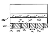
次に図4Dを参照すると、モノリシック集積ピクセル検出器210’’’の第4実施形態200’’’は、表面側216に読み出し部214と、裏面側220にピクセル化された吸収体218’’’を有するCMOS処理ウェハ212からなる。実施形態200’’’は、ウェハ製造に適した大面積単結晶の形態では成長できないが、幅w4のトレンチ254によって幅w3に隔てられたエピタキシャル吸収体パッチ252の形態のピクセル化されたエピタキシャル吸収体層218’’として大面積Si基板256上で成長可能な吸収体層218’’’に好適な実施形態である。各吸収体パッチ252の幅w3は、インプラント238によって定義されるピクセルサイズLよりも大きくても、同等でも、小さくてもよい。トレンチ254の幅w4は、各吸収体パッチ252の幅w3よりも好適には小さく、より好適にははるかに小さい。ARTの誘電体マスク開口部の間隔によって定義される吸収体パッチ252のために、トレンチの幅w4は、周知のリソグラフィおよび深反応性イオンエッチング技術で達成可能な最小幅、例えば1〜5μmに至るまで狭くてもよい。吸収体パッチ252の本質的に制約された横方向成長によって得られるトレンチの幅w4はさらに小さく、例えば100nm〜1μm、または20nm〜100nmであってもよい。
Next, referring to FIG. 4D, the fourth embodiment 200'''' of the monolithic integrated pixel detector 210'''' has a
実施形態200’’’は、Si基板256と格子的および熱的に不整合な吸収体層に最も好適な形態である。エピタキシャル吸収体層218’’’に最適な材料は、好適にはGe含有率が20%以上のSi1−xGex合金であってもよい。本実施形態の望ましい態様において、Si1−xGex合金は約0.6≦x≦0.8という高いGe含有量を有してもよい。約100〜200μmの厚みを有するこのようなSiGe合金が使用される場合、マンモグラフィーでの利用などのX線エネルギーが40keV以下に制限された適用にとりわけ適する。本実施形態のさらに望ましい態様では、Si1−xGex合金は約0.6≦x≦0.8という高いGe含有量まで組成傾斜され、任意的に、例えば直線的に傾斜された傾斜部の最終組成と等しいキャップ領域を有する。実施形態200’’’の最も望ましい態様において、Si基板256とピクセル化された吸収体218’’’の間のインターフェース258は、本質的に欠陥を有さない。これは、例えばピクセル化された吸収体218’’’を形成する半導体パッチ252の幅w3と傾斜率の両方を、吸収体218’’’がエピタキシャル成長する際のミスフィット応力の弾性的な緩和を可能にするほど十分に小さく選択することで達成できる(M.Salvalaglio,J.Appl.Phys.116,104306(2014)を例として参照し、開示された内容全体は本件に組み込まれる)。傾斜率は好ましくは約3%以下、約2%以下、または1%以下として選択される。本実施形態の他の態様では、基板256とピクセル化された吸収体218’’’のパッチ252の間のインターフェース領域258は、本質的に欠陥がない状態ではなくても、吸収体218’’’の金属化されたバック接点232’とCMOS処理ウェハ212のインプラント238に大きな電圧が印加された際に、暗電流を許容可能なレベルに抑えるのに十分小さいサイズとされる。当業者には周知のように、このような小さいインターフェース領域は、例えば貫通転位が窓の側壁でトラップされ、半導体がそこに向かって選択的に成長される誘電体マスク内に閉じ込められるアスペクト比トラッピング(ART)技術などによく利用される(I.Aberg et al.,IEDM San Francisco,2010を例として参照とし、開示された内容全体は本件に組み込まれる)。ARTの介助により、GaAs、CdTeまたはCdZnTeなどのSiGe以外の吸収体材料を用いることも可能となる。
Embodiment 200'''is the most suitable form for an absorber layer that is lattice and thermally inconsistent with the
トレンチ254の幅w4は、吸収体パッチ252の幅w3よりも好適には小さく(比率約1:2)、より好適にははるかに小さい(比率約1:10または約1:100)。自己抑制(self−limited)エピタキシャル成長工程と深掘パターニング基板が吸収体パッチ252のサイズw3を定義するために用いられる場合、トレンチの幅w4は1μm以下、または200nm以下、または100nm以下であってもよい(Von Kanelによる国際特許出願第WO2011/135432を例として参照し、開示された内容全体は本件に組み込まれる)。代替的に、ARTの方法が吸収体パッチ252のサイズw3を定義するために用いられる場合、トレンチ254の幅w4は誘電体窓の間隔によって定義されてもよく、誘電体マスクのパターニングに用いられるリソグラフィおよび深反応性イオンエッチング技術で達成可能な最小幅に至るほど狭くてもよい。CMOS処理ウェハ212の裏面側220および基板256は、密接な電気的接触を提供する共有結合250”によって、好適にはインターフェース状態をいくつか有するか全く有さないか、あるいは吸収体層218’’’とドリフト領域228の間におけるインターフェース間の電荷輸送を向上する(すなわちオーム挙動を得る)ために、ウェハ212の裏面側220全体に渡りインターフェース状態が例えば水素によって不動態化されて接合される。密接な電気接触が行われるためには、ウェハ212の裏面側220と吸収体層256の接合面は原子的に平坦で粒子のない状態で、尚且つ酸化物ゼロでなければならない。ウェハ212の裏面側220と吸収体層256の接合面には、酸化物ゼロの共有結合に必要とされる表面加工を行う前に、化学機械的研磨工程を施すことが勧められる。接合工程には、まだ酸化されていない表面の水分を低減するために任意的な仮接合アニール工程と、接合後アニール工程とが好ましくは含まれる。仮接合アニール工程および接合後アニール工程は低温で行われる。アニール温度は100℃から200℃、または200℃から300℃、または300℃から400℃の範囲とされる。いかなる場合も、CMOS処理されたウェハ212の金属化の分解を防ぐために、温度は約450℃以下でなくてはならない。各吸収体パッチ252は、吸収体ウェハの表面全体に渡って延長する金属化されたバック接点232’によって電気的に接続されてもよい。
The width w 4 of the trench 254 is preferably smaller (ratio about 1: 2) and more preferably much smaller (ratio about 1:10 or about 1: 100) than the width w 3 of the
吸収体218’’’の金属化されたバック接点232’に大きい電圧230が印加されると、吸収体ウェハ218’’’およびCMOS処理ウェハ212のドリフト領域228の空乏化につながり、吸収された高エネルギー物質粒子または光子によって生成された電子−正孔対は対応する電界において分離され、ピクセルのサイズLを定義するインプラント238および金属電極232’によってそれぞれ収集される。
When a
次に図5A〜5Gを参照すると、モノリシックピクセル検出器310の製造方法300は次の工程を含む。第1ステップ(図5A)では、好ましくは500Ωcm以上の抵抗率で軽くnドープまたは軽くpドープされたSiウェハ312は、電荷収集インプラント338の間隔によって定義されるサイズLの各ピクセルにその一部340が含まれる読み出し電子回路314を得るためにCMOS処理が施される。第2ステップ(図5B)では、ハンドリングウェハ360は、ウェハ312の任意で化学機械的研磨が施された表面側316に接合される。CMOSウェハ312の表面側316とハンドリングウェハ360の表面362との接合は永久的な接合ではなくても、第3ステップ(図5C)においてCMOSウェハ312を、例えば化学機械的研磨などによって軽くドープされた領域328’の厚みd1が200μm以下となるように薄層化するのに十分な強度を有していなければならない。本実施形態の好適な態様では、厚みd1は100μm以下、より好ましい態様では例えば10〜20μmに至るまで小さい。第4ステップ(図5D)では、薄層化されたCMOSウェハ312の裏面側320’と、共有結合に必要とされる化学機械的研磨および任意的な浅い水素注入が施されることも可能な(下面334を有する)厚みd2の吸収体ウェハ318の上面336に、例えば従来技術から周知の中性化プラズマによる表面酸化物のスパッタエッチングなどによって、酸化物ゼロの共有結合を行うための処理が行われる(C.Flotgen et al.によるECS Transactions 64,103(2014)を例として参照し、開示された内容全体は本件に組み込まれる)。第5ステップ(図5E)における好ましくは100℃から200℃の範囲、または200℃から300℃の範囲、または300℃から400℃の範囲の低温での任意的な仮接合アニール工程および接合後アニール工程によって、CMOS処理および薄層化されたウェハ312’の裏面側320’と吸収体ウェハ318の表面336との間で強力かつ導電性の接合350が提供される。任意的な接合後アニール工程は、例えば、オーム挙動が得られるようダングリングボンドを不動態化するために任意的に注入された水素を発生させることで、接合インターフェースに渡って電荷輸送を妨げるインターフェースバリアの排除に役立つこともある。
Next, referring to FIGS. 5A to 5G, the
吸収体材料がSiウェハ312’に対して熱膨張係数の不整合が大きいことを特徴とする場合、吸収体ウェハ318’はステップ6(図5F)として、望ましくない熱応力が加わるのを防ぐために、任意の接合後アニールの前に、幅w2のトレンチ354で隔たれた幅w1を有する個別のパッチ352の形態に任意でパターニングされてもよい。各吸収体パッチ352の幅w1は、インプラント338によって定義されるピクセルのサイズLよりも大きくても、同等でも、小さくてもよい。トレンチ354の幅w2は、吸収体パッチ352の幅w1よりも好適には小さく、より好適にはw1よりもはるかに小さい。トレンチ354の幅w2は、周知のリソグラフィおよび深反応性イオンエッチング技術で達成可能な最小幅に至るほど狭くてもよい(X.Li et al.,in Sensors and Actuators A87、139(2001)およびE.H.Klaaseen,in Sensors and Actuators A52,132(1996)を例として参照し、開示された内容全体は本件に組み込まれる)。各吸収体パッチ352の側壁374は、表面を不動態化することでピクセルセンサの作動時に漏洩電流を低減する誘電体膜376でコーティングされることが勧められる。第7ステップ(図5G)では、トレンチ354は任意で絶縁材372が充填されてもよく、金属接点332’は好適には各吸収体パッチ352を平行に接続する連続金属層として形成されてもよい。
If the absorber material is characterized by a large coefficient of thermal expansion mismatch with respect to the Si wafer 312', the absorber wafer 318' is in step 6 (FIG. 5F) to prevent unwanted thermal stress from being applied. , Arbitrarily patterned in the form of
吸収体ウェハ318’の金属化されたバック接点332’に大きい電圧330が印加されると、吸収体ウェハ318’および薄層化されたCMOS処理ウェハ312’のドリフト領域328’の空乏化につながり、吸収された高エネルギー物質粒子または光子によって生成された電子−正孔対は対応する電界において分離され、ピクセル検出器310のインプラント338に収集される。
When a
次に図6A〜6Kを参照すると、モノリシックピクセル検出器410の製造方法400は以下のステップを含むとされるが、開示される順番通りに実行される必要はない。第1ステップ(図6A)では、表面側416と裏面側420を有するSiウェハ412は、例えば好ましくは500Ωcm以上の抵抗率で軽くnドープまたはpドープされ、電荷収集インプラント438の間隔によって定義されるサイズLを有する各ピクセルにその一部440が含まれる読み出し電子回路414を得るためにCMOS処理が施される。第2ステップ(図6B)では、幅w4のトレンチ454によって隔たれた幅w3と高さh2を有する各パッチ452の形態でエピタキシャル成長される吸収体418の基板となるように、Si基板ウェハ456はパターニングおよび清浄されてもよい。各吸収体パッチ452の幅w3は、インプラント438によって定義されるピクセルのサイズLよりも大きくても、同等でも、小さくてもよい。従来技術から周知のように、自己抑制エピタキシャル成長工程と深掘パターニング基板が吸収体パッチ452のサイズw3を定義するために用いられる場合、トレンチの幅w4は1μm以下、または200nm以下、または100nm以下であってもよい(Von Kanelによる国際特許出願第WO2011/135432を例として参照し、開示された内容全体は本件に組み込まれる)。代替的に、ARTの方法が吸収体パッチ452のサイズw3を定義するために用いられる場合、トレンチの幅w4は誘電体窓の間隔によって定義されてもよく、リソグラフィおよび深反応性イオンエッチング技術で達成可能な最小幅に至るほど狭くてもよい(X.Li et al.,in Sensors and Actuators A87、139(2001)およびE.H.Klaassen,in Sensors and Actuators A52,132(1992)を例として参照し、開示された内容全体は本件に組み込まれる)。エピタキシャル成長が行われた後、各パッチ452の側壁474は、任意で誘電体不動態化層によって不動態化されてもよい。不動態化層は、一例としてピクセル検出器410が動作中に側壁474に沿った表面漏洩を制御するように設計された第1誘電体層436からなる。第1誘電体層は、熱酸化物または原子層蒸着(ALD)によって形成された酸化物であってもよい。任意的に、不動態化層は側壁474の環境的な影響に対する付加的な保護を提供する第2誘電体層476から構成されてもよい。それは、従来技術から周知のように原子層蒸着によって蒸着されるAl2O3から形成されてもよい。後に行われるウェハ接合工程のための処理として、吸収体層表面434に施される化学機械的研磨の任意の工程において安定性を提供するために、トレンチ454には誘電体充填材472が付加的に充填されてもよい。
Next, referring to FIGS. 6A-6K, the
図6Cを参照として第3ステップでは、Siウェハ412の表面側416は、後に行われる例えば化学機械的研磨工程などによるドリフト領域428の薄層化において機械的安定性を与えるために、ハンドリングウェハ460の表面462と接合される前に任意の化学機械的研磨が施される。図6Dを参照として類似する第4ステップ(図6D)では、エピタキシャル吸収体418の表面434は、例えば化学機械的研磨工程などによる基板456の薄層化において機械的安定性を与えるために、ハンドリングウェハ480の表面482に接合される。次に図6Eを参照として第5ステップでは、CMOS処理ウェハ412のドリフト領域428は、例えばプラズマエッチングや化学機械的研磨工程を行うことで薄層化される。薄層化されたドリフト領域428’を有する薄層化ウェハ412’の厚みはd1とされ、好ましくは約10〜100μm、より好ましくは約10〜20μmの範囲とされる。次に図6Fを参照として第6ステップでは、基板456’は、例えばプラズマエッチングや化学機械的研磨工程を行うことで薄層化される。薄層化基板456’の厚みはd2とされ、好ましくは約10〜100μm、より好ましくは約10〜20μmの範囲とされる。薄層化されたウェハ412’の表面420’および薄層化基板456’の表面490’は、任意的に浅い水素注入が施されてもよく、例えば従来技術から周知の中性化プラズマによる表面酸化物のスパッタエッチングなどによって、酸化物ゼロの共有結合を行うための処理が行われる(C.Flotgen et al.によるECS Trans.64,103(2014)を例として参照し、開示された内容全体は本件に組み込まれる)。図6Gを参照とした第7ステップでは、薄層化基板456’または薄層化CMOSウェハ412’は、任意の仮接合アニール後に表面の酸化物除去を行う前に、第8ステップ(図6H)で共有結合450によって接合されるべく、ウェハ接合のために準備された表面420’と490’が互いに向き合うように上下逆に返される。任意的な仮接合アニールおよび接合後アニール工程は双方ともに低温で行われる。アニール温度は100℃から200℃、または200℃から300℃、または300℃から400℃の範囲とされる。いかなる場合も、CMOS処理されたウェハ412の金属化の分解を防ぐために、温度は約450℃以下でなくてはならない。任意的な接合後アニール工程は、例えば、オーム挙動が得られるようダングリングボンドを不動態化するために任意的に注入された水素を発生させることで、接合インターフェースに渡って電荷輸送を妨げるインターフェースバリアの排除に役立つこともある。任意の接合後アニール工程の後、第9ステップ(図6I)においてハンドリングウェハ480は除去され、吸収体パッチ452の表面434は再び露出される。図6Jを参照とした第10ステップでは、吸収体パッチ452の表面434はハンドリングウェハ480の接合残渣を除去するための任意的な清浄工程にかけられる。その後、トレンチ454は、第2ステップ(図6B)ですでに充填材472が充填されている場合を除き、充填材472’で任意で充填される。最後に図6Kを参照とした第11ステップにおいて、ドリフト領域428’、456’および吸収体418を空乏化させるために高圧リード430が取り付けられた、連続する金属接点として作用する金属層432で吸収体パッチ452の表面434を金属化することで、完全なピクセル検出器410を得ることができる。
In the third step with reference to FIG. 6C, the
Si基板456に格子的にも熱的にも不整合のエピタキシャル吸収体層418のためのピクセル検出器410を製造するための方法としては、製造方法400が最も望ましい。吸収体層418の好適な材料は、好ましくはGe含有率が20%以上のSi1−xGex合金であってもよい。約0.6≦x≦0.8という高いGe含有量のSi1−xGex合金は、吸収体層418にとりわけ適した合金とされる。高Ge含有率のSi1−xGex合金から形成された100〜200μmの厚みを有する吸収体層が、マンモグラフィーなどの40keV以下のX線エネルギーに限定された適用に特に適切とされる。最も好ましいSi1−xGex合金は、約0.6≦x≦0.8という高いGe含有量xまで組成的に傾斜され、例えば直線的に傾斜された傾斜部の最終組成とほぼ等しいキャップ領域を有する。ピクセル検出器410の最も望ましい製造方法400において、Si基板456とピクセル化された吸収体418の間のインターフェース458は本質的に欠陥を有さないものとされる。ステップ状の勾配を有するSiGeナノ構造のより単純な例では効果的であると実証されているように、w3と傾斜率の両方を、吸収体418がエピタキシャル成長する際のミスフィット応力の弾性的な緩和を可能とするほど十分小さく選択することで、これを達成することかできる(M.Salvalaglio,J.Appl.Phys.116,104306(2014)を例として参照し、開示された内容全体は本件に組み込まれる)。傾斜率は、好ましくは約3%以下、約2%以下、または約1%以下で選択されてもよい。本実施形態の他の態様では、基板456とピクセル化された吸収体418のパッチ452の間のインターフェース領域458は、本質的に欠陥がない状態ではなくても、吸収体418の金属化されたバック接点432と薄層化CMOS処理ウェハ412’のインプラント438に大きな電圧を印加した際に暗電流を許容可能なレベルに抑えるのに十分小さいサイズとされる。このような小さなインターフェース領域は、例えば貫通転位が窓の側壁でトラップされ、半導体がそこに向かって選択的に成長される誘電体マスク内に閉じ込められるアスペクト比トラッピング(ART)技術などによく利用される(I.Aberg et al.,IEDM San Francisco,2010を例として参照とし、開示された内容全体は本件に組み込まれる)。ARTの介助により、GaAs、Ge、CdTeまたはCdZnTeなどのSiGe以外の吸収体材料を用いることも可能となる。
The
次に図7A〜7Hを参照すると、モノリシックピクセル検出器510の代案的な製造方法500は以下のステップを含むとされるが、開示される順番通りに実行される必要はない。図7Aを参照すると、第1ステップでは、表面側516と裏面側520を有するSiウェハ512は、例えば好ましくは500Ωcm以上の抵抗率で軽くnドープまたは軽くpドープされ、電荷収集インプラント538の間隔によって定義されるサイズLを有する各ピクセルに、その一部540が含まれる読み出し電子回路514を得るためにCMOS処理が施される。次に第7Bを参照すると、第2ステップでは、Siウェハ556が、吸収体518がSi基板556とのインターフェース558を形成する個別の吸収体パッチ552の形態でエピタキシャル成長する基板となるように、Siウェハ556はパターニングされてもよい。パッチ552は幅w3と高さh2を有し、幅w4のトレンチ554によって隔たれてなる。各吸収体パッチ552の幅w3は、インプラント538によって定義されるピクセルのサイズLよりも大きくても、同等でも、小さくてもよい。吸収体パッチ552の高さは約20〜50μm、好ましくは約50〜100μm、さらに好ましくは約100〜200μmとされる。従来技術から周知のように、自己抑制エピタキシャル成長工程と深掘パターニング基板が吸収体パッチ552のサイズw3を定義するために用いられる場合、トレンチの幅w4は1μm以下、または200nm以下、または100nm以下とされる(Von Kanelによる国際特許出願第WO2011/135432を例として参照し、開示された内容全体は本件に組み込まれる)。代替的に、ARTの方法が吸収体パッチ552のサイズw3を定義するために用いられる場合、トレンチの幅w4は誘電体窓の間隔によって定義されてもよく、リソグラフィおよび深反応性イオンエッチング技術で達成可能な最小幅に至るほど狭くてもよい(X.Li et al.,in Sensors and Actuators A87、139(2001)およびE.H.Klaassen,in Sensors and Actuators A52,132(1992)を例として参照し、開示された内容全体は本件に組み込まれる)。エピタキシャル成長が行われた後、各パッチ552の側壁574は、任意で誘電体不動態化層によって不動態化されてもよい。不動態化層は、一例としてピクセル検出器510が動作中に側壁574に沿った表面漏洩を制御するように設計された第1誘電体層536から構成されることも可能である。第1誘電体層は熱酸化物または原子層蒸着(ALD)によって形成された酸化物であってもよい。任意的に、不動態化層は、側壁574の環境的な影響からの付加的な保護を提供する第2誘電体層576から構成されてもよい。それは、従来技術から周知のように、原子層蒸着によって蒸着されるAl2O3から形成されてもよい。後に行われるウェハ接合のための処理として、吸収体表面534に施される化学機械的研磨の任意の工程において安定性を提供するために、トレンチ554には誘電体充填材572が付加的に充填されてもよい。
Next, referring to FIGS. 7A-7H, the
次に図7Cを参照すると、第3ステップでは、Siウェハ512の表面516には、後に行われる、例えば化学機械的研磨工程などのドリフト領域528の薄層化において機械的安定性を与えるために、ハンドリングウェハ560の表面562と接合される前に任意で化学機械的研磨が施される。第7Dを参照として第4ステップでは、エピタキシャル吸収体518の表面534は化学機械的研磨工程にかけられ、それによりエピタキシャル吸収体の高さは、例えば高さh3から1〜4μmだけわずかに低減される。次に図7Eを参照とした第5ステップでは、CMOS処理ウェハ512のドリフト領域528は、例えばプラズマエッチングまたは化学機械的研磨工程などによって薄層化される。ドリフト領域528’を有する薄層化ウェハ512’の厚みはd1とされ、好ましくは約10〜100μm、より好ましくは約10〜20μmの範囲とされる。第6ステップでは、薄層化ウェハ512’の表面520’および吸収体518の表面534は任意的に浅い水素注入が施され、例えば従来技術から周知のように(C.Flotgen et al.によるECS Transactions 64,103(2014)を例として参照し、開示された内容全体は本件に組み込まれる)中性化プラズマにより表面酸化物をスパッタエッチングすることで共有結合のための処理が施され、任意の仮接合アニール工程の後に共有結合550で接合される(図7F)。共有結合550には、任意の接合後アニール工程が施されてもよい。任意の仮接合アニール工程および接合後アニール工程は双方ともに低温で行われる。アニール温度は100℃から200℃の範囲、または200℃から300℃の範囲、または300℃から400℃の範囲とされる。いかなる場合も、CMOS処理されたウェハ512’の金属化の分解を防ぐために、温度は約450℃以下でなくてはならない。任意的な接合後アニール工程は、例えば、オーム挙動が得られるようにダングリングボンドを不動態化するために任意的に注入された水素を発生させることで、接合インターフェースに渡って電荷輸送を妨げるインターフェースバリアの排除に役立つこともある。任意の接合後アニール工程が行われた後、第7ステップにおいて、吸収体パッチ552の表面558’を露出させるように化学機械的研磨あるいはプラズマエッチングによって、エピタキシャル吸収体518の基板556は除去されてもよい(図7G)。特に基板512、512’とのインターフェースに欠陥を有する場合、高さをh4に低減するために、上記エッチング工程で吸収体パッチ552の一部をエッチングで除去することが好ましい。このエッチング工程により、ミスフィット転位だけでなく貫通転位もまた除去されるように、高さh4は高さh3よりも数μmだけ小さい数値とされる。図7Hを参照すると、第8ステップでは、ドリフト領域528および吸収体518を空乏化させるための高圧リード530が取り付けられることも可能な、金属接点として作用する金属層532を備えた吸収体パッチ552の表面558’を金属化することで、完全なピクセル検出器510を得ることができる。
Next, referring to FIG. 7C, in the third step, the
ピクセル検出器510の製造方法500は、検出器の動作中に薄層化ドリフト領域528’の厚みd1と吸収体パッチ552の高さh4のみが空乏化されればよいという利点を有する。また、Si基板556と格子的および熱的に不整合の吸収体層518のためのピクセル検出器510に好ましい製造方法でもある。吸収体層518に好ましい材料は、好ましくはGe含有率が20%以上のSi1−xGex合金であってもよい。約0.6≦x≦0.8という高いGe含有量を有するSi1−xGex合金は、エピタキシャル吸収体層518に特に適した合金とされる。このような高いGe含有率を有するSi1−xGex合金からなる約100〜200μmの厚みを有する吸収体層は、マンモグラフィーでの利用などのX線エネルギーが40keV以下に制限された適用にとりわけ適する。最も好ましいSi1−xGex合金は、約0.6≦x≦0.8という高いGe含有量まで組成傾斜され、任意的には 例えば直線的に傾斜された傾斜部の最終組成と等しいキャップ領域を有する。ピクセル検出器510の最も好ましい製造方法500において、Si基板556とピクセル化された吸収体518の間のインターフェース558は本質的に欠陥を有さない。ステップ状の勾配を有するSiGeナノ構造のより単純な例では効果的であると実証されているように(M.Salvalaglio,J.Appl.Phys.116,104306(2014)を例として参照し、開示された内容全体は本件に組み込まれる)、ピクセル化された吸収体518を形成する半導体パッチ552の幅w3と傾斜率の両方を、吸収体518がエピタキシャル成長する際のミスフィット応力の弾性的な緩和を可能とするほど十分小さく選択することで、これを達成することかできる。傾斜率は約3%以下、より好ましくは約2%以下または1%以下で選択されることが好ましい。本実施形態の他の態様では、基板556とピクセル化された吸収体518のパッチ552の間のインターフェース領域558は、本質的に欠陥がない状態ではなくても、吸収体518の金属化されたバック接点532と薄層化CMOS処理ウェハ512’のインプラント538に大きな電圧を印加した際に暗電流を許容可能なレベルに抑えるのに十分小さいサイズとされる。当業者には周知のように、このような小さなインターフェース領域は、例えば貫通転位が窓の側壁でトラップされ、半導体がそこに向かって選択的に成長される誘電体マスク内に閉じ込められるアスペクト比トラッピング(ART)技術などによく利用される(I.Aberg et al.,IEDM San Francisco,2010を例として参照とし、開示された内容全体は本件に組み込まれる)。ARTの介助により、GaAs、CdTeまたはCdZnTe合金などのSiGe以外の吸収体材料を用いることも可能となる。
(モノリシックCMOS集積ピクセル検出器を備えた光子計数CBCTの例示的な適用)
本発明のCBCTは、以下に記載される人間または動物のいずれかの医療用途、そして以下で説明されるその他の用途のための方法に組み込まれると共に使用される。
(Example application of photon counting CBCT with monolithic CMOS integrated pixel detector)
The CBCTs of the present invention are incorporated and used in methods for any of the human or animal medical uses described below, as well as other uses described below.
(投影X線撮影法(projection radiography)の実施例)
本発明のCBCTは、被写体を透過するX線がデジタル情報を生成する電気信号に変換され、さらに局所的または遠隔的にコンピュータの画面上に表示される画像に変換されるデジタルX線撮影システムとして用いられる。
(Example of projection radiography)
The CBCT of the present invention is a digital X-ray imaging system in which X-rays transmitted through a subject are converted into electrical signals that generate digital information, and further converted into images locally or remotely displayed on a computer screen. Used.
単純X線撮影に本発明のCBCTを用いたシステムおよび方法を組み合わせることで、典型的な診断が得られる病態は数多くある。それらのシステムおよび方法の例としては、様々な種類の関節炎、肺炎、骨腫瘍、骨折、先天性骨格異常およびその類の病理を診断するものを含む。 There are many pathological conditions for which a typical diagnosis can be obtained by combining simple X-ray photography with the system and method using the CBCT of the present invention. Examples of such systems and methods include those that diagnose various types of arthritis, pneumonia, bone tumors, bone fractures, congenital skeletal abnormalities and the like.
(画像化治療の実施例)
モノリシックCMOS集積ピクセル検出器を導入することで、X線透視装置の設計においてヨウ化セシウム(CsI)スクリーンの置換が可能となる。このため、応用分野は同様であっても、本発明のCBCTの定義としては「X線透視装置」よりも「4次元CT」(4DCT)の方がより正確とされる。モノリシックCMOS集積ピクセル検出器を備えた光子計数CBCTは、運動中の解剖学的構造のリアルタイムでの撮像を可能とし、この方法は任意で造影剤によって増補される。造影剤は、解剖学的な輪郭の描写および血管や例えば泌尿生殖システムまたは胃腸管などの様々なシステムの機能をみるために、嚥下または患者の体内に注射されて投与される。現在常用されている造影剤には2つある。バリウム硫酸(BaSo4)は胃腸管の評価のために被検体に経口または直腸から投与される。様々な配合のヨウ素は、経口、直腸、動脈内、静脈内の経路から投与される。これらの造影剤はX線を吸収または散乱し、リアルタイム撮像に伴い、血管系における消化管または血流内の力学的な生理的工程の撮像を可能にする。また、ヨード造影剤は、異常(例えば腫瘍、嚢胞、炎症部など)が可視できるように、異常部位では通常の組織とは異なる濃度で濃縮される。
(Example of imaging treatment)
The introduction of a monolithic CMOS integrated pixel detector allows the replacement of cesium iodide (CsI) screens in the design of fluoroscopes. Therefore, even if the fields of application are the same, the definition of CBCT of the present invention is that "four-dimensional CT" (4DCT) is more accurate than "X-ray fluoroscope". Photon counting CBCT with a monolithic CMOS integrated pixel detector allows real-time imaging of anatomical structures during motion, the method of which is optionally augmented with contrast media. Contrast agents are swallowed or injected into the patient's body for anatomical contouring and functioning of blood vessels and various systems such as the genitourinary system or gastrointestinal tract. There are two types of contrast media currently in common use. Barium sulfate (BaSo 4 ) is administered to the subject orally or rectally for evaluation of the gastrointestinal tract. Various formulations of iodine are administered by oral, rectal, arterial and intravenous routes. These contrast agents absorb or scatter X-rays, allowing imaging of mechanical physiological steps in the gastrointestinal tract or bloodstream in the vascular system with real-time imaging. In addition, the iodine contrast medium is concentrated at a concentration different from that of normal tissue at the abnormal site so that abnormalities (for example, tumors, cysts, inflamed areas, etc.) can be seen.
より一般的には、CBCTは画像化治療システムおよび方法において使用される。画像化治療には、本件で説明されたピクセル検出器を有するシステムおよび方法を用いた画像化システムによってガイドされる低侵襲処置が含まれる。それらの処置は診断的なものか、血管造影法や血管形成法などの治療やそれに用いられるシステムに関する。この例示的なシステムは、末梢血管疾患、腎動脈狭窄、下大静脈フィルター配置、胃瘻チューブ配置、胆管ステント介入および肝性介入(hepatic intervention)を診断および/または治療するためのシステムを含む。また、画像誘導型の整形、胸部、腹部、頭頸部および神経の外科処置や、生検、近接照射治療、体外放射線治療、経皮ドレナージおよびステント配置、または高周波アブレーションなどの非血管造影処置も含まれる。ピクセル検出器を用いたシステムの介助により生成された画像は、誘導のために用いられる。ピクセル検出器の介助により生成された画像は、介入的な放射線科医が被検体の病状が見られる部位まで体内に機器を誘導することを可能にするマップを提供する。これらのシステムおよび方法により、例えば血管造影的介入のある処置、画像誘導型の整形、胸部、腹部、頭頸部および神経の外科処置や、生検、近接照射治療、体外放射線治療、経皮ドレナージおよびステント配置、または高周波アブレーションなどの非血管造影処置において、被検体の身体的組織の外傷を最小限に抑え、感染率、回復期間および入院日数を低減する。 More generally, CBCT is used in imaging therapy systems and methods. Imaging therapies include minimally invasive procedures guided by imaging systems using the systems and methods with pixel detectors described in this case. These procedures are diagnostic or relate to treatments such as angiography and angioplasty and the systems used in them. This exemplary system includes a system for diagnosing and / or treating peripheral vascular disease, renal artery stenosis, inferior vena cava filter placement, gastrostomy tube placement, bile duct stent intervention and hepatic intervention. It also includes image-guided plastic surgery, chest, abdomen, head and neck and nerve surgery, and non-angiographic procedures such as biopsy, proximity radiation therapy, extracorporeal radiation therapy, percutaneous drainage and stent placement, or high frequency ablation. Is done. Images generated with the help of a system with pixel detectors are used for guidance. The images generated with the assistance of a pixel detector provide a map that allows an intervening radiologist to guide the device into the body to the site where the subject's condition is seen. These systems and methods allow, for example, procedures with angiographic interventions, image-guided orthopedics, chest, abdomen, head and neck and nerve surgery, biopsy, proximity radiation therapy, extracorporeal radiation therapy, percutaneous drainage and Minimize trauma to the body tissue of the subject and reduce infection rate, recovery time and length of stay in non-angiographic procedures such as stent placement or high frequency ablation.
以下の米国特許文献、外国特許文献およびその他の公開文書は参照により、本件に記載されたかのように本件に組み込まれ、依拠される。
米国特許文献
5,712,484 1/1998 Harada他
6,787,885 B2 9/2004 Esser他
8,237,126 B2 8/2012 von Kanel他
8,378,310 B2 2/2009 Bornefalk他
8,792,965 B2 7/2014 Ning他
その他の特許文献
EP0571135 A2 11/1993 Collins他
WO02/067271 A2 8/2002 Ruzin
EP1691422 A1 8/2006 Yasuda他
WO2006117720 A2 11/2006 Proksa他
WO2011102779 A1 8/2011 Danielsson他
WO2011/135432 A1 11/2011 von Kanel他
WO2014123726 A1 8/2014 Ning他
付加的な公開文書
http://medipix.web.cern.ch
http://www.canberra.com/products/detectors/germanium-detectors.asp
http://.dectris.ch
ttp://www.healthcare.philips.com
Alig R.C. et
al., “Scattering by ionization and phonon emission in semiconductors”, Physical
Review B 22, 5565 (1980)
Alig R.C.
“Scattering by ionization and phonon emission in semiconductors. II. Monte
Carlo calculations”, Physical Review B 27, 968 (1983)
Baba R. et al.:
Comparison of flat-panel detector and image-intensifier detector for cone-beam
CT, Comp. Med. Imaging and Graphics 26, 153 (2002)
Bale D.S. et
al.: Nature of polarization in wide bandgap semiconductor detectors under
high-flux irradiation: Application to semi-insulating Cd1-xZnxTe,
Phys. Rev. B 77, 035205 (2008)
Ballabriga R.
et al. “The Medipix3RX: a high resolution, zero dead-time pixel detector
readout chip allowing spectroscopic imaging”, 2013, JINST 8 C02016
Bertolucci E.
et al.: GaAs Pixel radiation detector as an autoradiography tool for genetic
studies, Nucl. Sci. Meth. Phys. Res. A 422, 242 (1999)
Bornefalk H./
Danielsson M.: Photon-counting spectral computed tomography using slicon strip
detectors: a feasibility study, Phys. Med. Biol. 55, 1999 (2010)
Cho Hyo-Min et
al., <Charactristic performance evaluation of a photon counting Si strip
detector for low dose spectral breast CT imaging>, Med. Phys. Sep. 2014; 41
(9), 091903
Colace L. et
al., “Low Dark-Current Germanium-on-Silicon Near-Infrared Detectors”, IEEE
Photonics Technology Letters 19, 1813-1815 (2007)
Falub C. V. et
al., “Perfect crystals grown from imperfect interfaces”, Scientific Reports 3,
2276 (2013)
Fitzgerald E.
A. et al.: Totally relaxed GexSi1-x layers with low
threading dislocation densities grown on Si substrates, Appl. Phys., Letter 59,
811 (1991)
Flotgen C. et al., “Novel surface preparation
methods for covalent and conductive bonded interfaces fabrication”, ECS
Transactions 64, 103-110 (2014)
Gros d’Allion E
et al.: Development and characterization of a 3D GaAs
X-ray
detector for medical imaging, Nucl. Instr. Meth. Phys. Res. A 727, 126 (2013)
Gupta R. et
al.: Ultra-high resolution flat-panel volume CT: fundamental principles, design
architecture, and system characterization, Eur. Radiol. 16, 1191 (2006)
Hamann E. et
al.: Performance of a Medipix3RX Spectroscopic Pixel Detector with a High
Resistivity Gallium Arsenide Sensor, IEEE Trans. Med. Imaging 34, 707, (2015)
Henry D. et
al., “TSV Last for Hybrid Pixel Detectors: Application to Particle Physics and
Imaging Experiments” in IEEE Electronic Components & Technology Conference,
568 (2013)
Hirota S. et
al.: Cone-Beam CR with Flat-Panel-Detector Digital Angiography System: Early
Experience in Abdominal Interventional Procedures, Cardiovasc, Intervent.
Radiol. 29, 1034 (2006)
Isa F. et al.:
From plastic to elastic stress relaxation in highly mismatched SiGe/Si
Heterostructures, Acta Materialia 114, 97-105 (2016)
Jiang T et al.,
“Hydrogenation of interface states at a clean grain boundary in the direct
silicon bonded wafer Phys. Sts. Sol. A 209, 990-993 (2012)
Kasap S. et
al., “Amorphous and polycrystalline photoconductors for direct conversion flat
panel X-ray image sensors”, Sensors 11, 5112-5157 (2011)
Klaassen E. H.
et al., “Silicon fusion bonding and deep reactive ion etching: a new technology
for microstructures”, Sensors and Actuators A52, 132-139 (1996)
Kreiliger T et
al., “Individual heterojunctions of 3D germanium crystals on silicon CMOS for
monolithically integrated X-ray detector”, Physica Status Solidi A 211, 131-135
(2014)
Liu X. et al.: A
Silicon-Strip Detector for Photon-Counting Spectral CT: energy Resolution From
40keV to 120keV, IEEE Transactions on Nuclear Science, vol. 61, issue 3,
pp.1099-1105 (2014)
Loshachenko A
et al., “Impact of hydrogen on electrical levels and luminescence of
dislocation network at the interface of hydrophilically bonded silicon wafers”,
Phys. Stat. Sol. C 10, 36 (2013)
Mattiazzo S. et
al., “LePIX: First results from a novel monolithic pixel sensor”, Nuclear
Instruments and Methods in Physics Research A 718, 288-291 (2013)
Orth R. C. et
al.: C-arm Cone-beam CT: General Principles and Technical Considerations for
Use in Interventional Radiology, J. Vasc Interv. Radiol. 19, 814 (2008)
Pennicard D. et
al.: Development of LAMBDA: Large Area Medipix-Based Detector Array, 2012 JINST
6, C11009
Procz S. et
al., “Medipix3 CT for material sciences”, 2013 JINST, 8 C01025
Salvalaglio M.
et al., “Fine control of plastic and elastic relaxation in Ge/Se vertical
heterostructures” Journal of Applied Physics 116, 104306 (2014)
Sechopoulos I.
“A review of breast tomosynthesis” Med Phys. 2013 Jan; 40(1): 014302
Taguchi K./
Iwanczyk J.: “Vision 20/20: Single photon counting x-ray detectors in medical
imaging”, Med Phys. Oct 2013; 40(10) 100901
Veale, M. C. et
al., Chromium compensated gallium arsenide detectors for X-ray and γ-ray spectroscopic imaging, Nucl Inst. Meth. Phys. Res, A 752,
6 (2014)
Vykydal Z. et
al. in Nucl Instr. Meth. In Phys. Res. A 591, 241 (2008)
Weber J et.
Al., “Near-band-gap photoluminescence of Si-Ge alloys”, Physical review B 40,
5683-5693 (1989)
The following US patent documents, foreign patent documents and other published documents are incorporated and relied upon in this case by reference as if they were described in this case.
U.S. Patent Documents 5,712,484 1/1998 Harada et al. 6,787,885
Other Patent Documents EP0571135 A2 11/1993 Collins et al. WO 02/067271 A2 8/2002 Ruzin
EP1691422 A1 8/2006 Yasuda et al. WO20061177720 A2 11/2006 Proksa et al. WO2011102779 A1 8/2011 Danielsson et al. WO2011 / 135432 A1 11/2011 von Kanel et al. WO2014123726 A1
Additional public documents
http://medipix.web.cern.ch
http://www.canberra.com/products/detectors/germanium-detectors.asp
http://.dectris.ch
ttp: //www.healthcare.philips.com
Alig RC et
al., “Scattering by ionization and phonon emission in semiconductors”, Physical
Alig RC
“Scattering by ionization and phonon emission in semiconductors. II. Monte
Carlo calculations ”, Physical Review B 27, 968 (1983)
Baba R. et al .:
Comparison of flat-panel detector and image-intensifier detector for cone-beam
CT, Comp. Med. Imaging and
Bale DS et
al .: Nature of polarization in wide bandgap semiconductor detectors under
high-flux irradiation: Application to semi-insulating Cd 1-x Zn x Te,
Phys. Rev. B 77, 035205 (2008)
Ballabriga R.
et al. “The Medipix3RX: a high resolution, zero dead-time pixel detector
Spectrochip allowing spectroscopic imaging ”, 2013, JINST 8 C0 2016
Bertolucci E.
et al .: GaAs Pixel radiation detector as an autoradiography tool for genetic
studies, Nucl. Sci. Meth. Phys. Res. A 422, 242 (1999)
Bornefalk H./
Danielsson M .: Photon-counting spectral computed tomography using slicon strip
detectors: a feasibility study, Phys. Med. Biol. 55, 1999 (2010)
Cho Hyo-Min et
al., <Charactristic performance evaluation of a photon counting Si strip
detector for low dose spectral breast CT imaging>, Med. Phys. Sep. 2014; 41
(9), 091903
Colace L. et
al., “Low Dark-Current Germanium-on-Silicon Near-Infrared Detectors”, IEEE
Photonics Technology Letters 19, 1813-1815 (2007)
Falub CV et
al., “Perfect crystals grown from imperfect interfaces”,
2276 (2013)
Fitzgerald E.
A. et al .: Totally relaxed Ge x Si 1-x layers with low
threading dislocation densities grown on Si recently, Appl. Phys.,
811 (1991)
Flotgen C. et al., “Novel surface preparation
methods for covalent and conductive bonded interfaces fabrication ”, ECS
Gros d'Allion E
et al .: Development and characterization of a 3D GaAs
X-ray
detector for medical imaging, Nucl. Instr. Meth. Phys. Res. A 727, 126 (2013)
Gupta R. et
al .: Ultra-high resolution flat-panel volume CT: fundamental principles, design
architecture, and system characterization, Eur. Radiol. 16, 1191 (2006)
Hamann E. et
al .: Performance of a Medipix3RX Spectroscopic Pixel Detector with a High
Resistivity Gallium Arsenide Sensor, IEEE Trans. Med.
Henry D. et
al., “TSV Last for Hybrid Pixel Detectors: Application to Particle Physics and
Imaging Experiments ”in IEEE Electronic Components & Technology Conference,
568 (2013)
Hirota S. et
al .: Cone-Beam CR with Flat-Panel-Detector Digital Angiography System: Early
Experience in Abdominal Interventional Procedures, Cardiovasc, Intervent.
Radiol. 29, 1034 (2006)
Isa F. et al .:
From plastic to elastic stress relaxation in highly mismatched SiGe / Si
Heterostructures, Acta Materialia 114, 97-105 (2016)
Jiang T et al.,
“Hydrogenation of interface states at a clean grain boundary in the direct
silicon bonded wafer Phys. Sts. Sol. A 209, 990-993 (2012)
Kasap S. et
al., “Amorphous and preferably photoconductors for direct conversion flat
panel X-ray image sensors ”, Sensors 11, 5112-5157 (2011)
Klaassen EH
et al., “Silicon fusion bonding and deep reactive ion etching: a new technology
for microstructures ”, Sensors and Actuators A52, 132-139 (1996)
Kreiliger T et
al., “Individual heterojunctions of 3D germanium crystals on silicon CMOS for
monolithically integrated X-ray detector ”, Physica Status Solidi A 211, 131-135
(2014)
Liu X. et al .: A
Silicon-Strip Detector for Photon-Counting Spectral CT: Energy Resolution From
40keV to 120keV, IEEE Transactions on Nuclear Science, vol. 61,
pp.1099-1105 (2014)
Loshachenko A
et al., “Impact of hydrogen on electrical levels and luminescence of
dislocation network at the interface of hydrophilicly bonded silicon wafers ”,
Phys. Stat.
Mattiazzo S. et
al., “LePIX: First results from a novel monolithic pixel sensor”, Nuclear
Instruments and Methods in Physics Research A 718, 288-291 (2013)
Orth RC et
al .: C-arm Cone-beam CT: General Principles and Technical Considerations for
Use in Interventional Radiology, J. Vasc Interv. Radiol. 19, 814 (2008)
Pennicard D. et
al .: Development of LAMBDA: Large Area Medipix-Based Detector Array, 2012 JINST
6, C11009
Procz S. et
al., “Medipix3 CT for material sciences”, 2013 JINST, 8 C01025
Salvalaglio M.
et al., “Fine control of plastic and elastic relaxation in Ge / Se vertical
heterostructures ”Journal of Applied Physics 116, 104306 (2014)
Sechopoulos I.
“A review of breast tomosynthesis” Med Phys. 2013 Jan; 40 (1): 014302
Taguchi K./
Iwanczyk J .: “
imaging ”, Med Phys. Oct 2013; 40 (10) 100901
Veale, MC et
al., Chromium compensated gallium arsenide detectors for X-ray and γ-ray spectroscopic imaging, Nucl Inst. Meth. Phys. Res, A 752,
6 (2014)
Vykydal Z. et
al. in Nucl Instr. Meth. In Phys. Res. A 591, 241 (2008)
Weber J et.
Al., “Near-band-gap photoluminescence of Si-Ge alloys”,
5683-5693 (1989)
(ゲルマニウム検出器)
図8はゲルマニウム検出器の例の斜視図を示す。
(Germanium detector)
FIG. 8 shows a perspective view of an example of a germanium detector.
(序文)
ゲルマニウム検出器は、p−i−n構造を有する半導体ダイオードであり、その真性(i)領域は特にX線およびガンマ線などの電離放射線に対する感応性を有する。逆バイアス下において、電界は真性領域または空乏化領域に渡って延長する。検出器の空乏化された体積内で光子が材料と相互作用すると、電荷キャリア(正孔と電子)が生成され、電界によってpおよびn電極へ移動される。この電荷は、入射する光子によって検出器に堆積されるエネルギーに比例し、積分電荷有感型プリアンプによって電圧パルスに変換される。
(preface)
The germanium detector is a semiconductor diode having a p-in structure, and its intrinsic (i) region is particularly sensitive to ionizing radiation such as X-rays and gamma rays. Under reverse bias, the electric field extends over the true or depleted region. When photons interact with the material within the depleted volume of the detector, charge carriers (holes and electrons) are generated and transferred by the electric field to the p and n electrodes. This charge is proportional to the energy deposited on the detector by the incident photons and is converted into voltage pulses by the integrated charge-sensitive preamplifier.
ゲルマニウムは比較的低いバンドギャップを有するため、電荷キャリアの熱的生成(従って逆漏れ電流)を許容可能なレベルまで低下させるために、検出器は冷却されなければならない。さもなければ、漏れ電流から発生するノイズによって検出器のエネルギー分解能が破壊されてしまう。図9は「一般的な分解能対エネルギー」を示した図である。77°Kの温度を有する液体窒素は、このような検出器のための冷却媒体として一般的に用いられる。検出器は、LN2デュワに取り付けられるか、挿入された真空チャンバに設けられる。感応性検出器の表面は、このように水分および凝縮性汚染物質から保護される。 Due to the relatively low bandgap of germanium, the detector must be cooled in order to reduce the thermal production of charge carriers (and thus the back leakage current) to acceptable levels. Otherwise, the noise generated from the leakage current will destroy the energy resolution of the detector. FIG. 9 is a diagram showing “general resolution vs. energy”. Liquid nitrogen with a temperature of 77 ° K. is commonly used as a cooling medium for such detectors. The detector is mounted in an LN2 dewar or installed in an inserted vacuum chamber. The surface of the sensitive detector is thus protected from moisture and condensable contaminants.
ゲルマニウム検出器
(ゲルマニウム検出器の種別)
キャンベラ社は業界で最も多くの種類の検出器を提供している。適切な技術を材料および処理技術の両方に用いることで、キャンベラ社は幅広い用途に最適となる検出器を提供することが可能である。このような多種多様な製品を得るために、p型とn型の両方のゲルマニウムと、拡散、注入およびバリア接点(barrier contact)式のものが用いられる。
Germanium detector (type of germanium detector)
Canberra offers the largest variety of detectors in the industry. By using the right technology for both materials and processing technologies, Canberra can provide detectors that are optimal for a wide range of applications. In order to obtain such a wide variety of products, both p-type and n-type germanium and diffusion, injection and barrier contact type germanium are used.
(クライオスタット)
液体窒素クライオスタットは、Ge検出器システムの信頼性のある長期的なパフォーマンスを保証するうえで、最も重要でおそらく最も評価されていない要素であるだろう。キャンベラ社は、最も過酷な動作条件における検出器の長寿命を保証する厳しい品質基準で、独自のクライオスタットを製造している。
(Cryostat)
Liquid nitrogen cryostats are probably the most important and perhaps the least valued factor in ensuring reliable long-term performance of Ge detector systems. Canberra manufactures its own cryostats with strict quality standards that guarantee the longevity of the detector in the harshest operating conditions.
標準的なキャンベラ社のクライオスタットは、コンパクトシリンダに検出器チャンバとプリアンプが共に搭載されるスリムデザイン型である。 The standard Canberra cryostat is a slim design with a compact cylinder and a detector chamber and preamplifier.
Ultra−LEGeやSi(Li)などの低エネルギー検出器には、この種別の検出器に関連する小径(25mm)のエンドキャップに互換性のあるフランジ型クライオスタットが用いられる。フランジ型クライオスタットは、検出器のその他の種類でも別途有料のオプションとして入手可能である。 For low energy detectors such as Ultra-LEGe and Si (Li), flanged cryostats compatible with the small diameter (25 mm) end caps associated with this type of detector are used. Flangeed cryostats are also available as a separate paid option for other types of detectors.
キャンベラ社は、小真空チャンバに搭載された検出器と併せて、当分野で再構成されることが可能な変換式クライオスタットの一連の製品も提供する。 Canberra also offers a range of convertible cryostats that can be reconfigured in the art, along with detectors mounted in small vacuum chambers.
液体窒素不使用の操作を求められる適用には、CryolectricIIがキャンベラ社から提供される。この電気的に冷却されるクライオスタットは、CFCを有さない冷却材を使用し、産業上および実験室での用途に適する。 Cryometric II is provided by Canberra for applications that require liquid nitrogen-free operation. This electrically cooled cryostat uses a CFC-free coolant and is suitable for industrial and laboratory applications.
図10は「構造コード」および「検出器の種類」に関する情報を表示する。 FIG. 10 displays information about the "structural code" and the "detector type".
図11は「線源からエンドキャップまでの間隔が2.5cmの様々なGe検出器の典型的な絶対効率曲線」を描いた図を示す。 FIG. 11 shows a diagram depicting "a typical absolute efficiency curve of various Ge detectors with a distance of 2.5 cm from the source to the end cap".
ゲルマニウム検出器
(プリアンプ)
Ge検出器で使用されるプリアンプには2つの種類しかない。これらは、インテグレータを放電するために動的な充電回復(RCフィードバック)またはパルス式の充電回復(パルス式光学またはトランジスタリセット)のいずれかの方法を用いる電荷感応型プリアンプである。以下の図は、フィードパック抵抗器の数値と約20ボルトに制限されたインテグレータの動的出力電圧範囲の関数である、分離されたRCフィードバックプリアンプのエネルギー比率の限界を表す。
Germanium detector (preamplifier)
There are only two types of preamplifiers used in Ge detectors. These are charge-sensitive preamplifiers that use either dynamic charge recovery (RC feedback) or pulsed charge recovery (pulse optics or transistor reset) to discharge the integrator. The figure below shows the limit of the energy ratio of the separated RC feedback preamplifier, which is a function of the feedpack resistor value and the integrator's dynamic output voltage range limited to about 20 volts.

エネルギー比率の限界は、低い数値の帰還抵抗を選択することで大幅に上げることができるが、もちろんそれに伴いノイズも増加する。図12は一般的な検出器の実際のパフォーマンスデータを示す。 The limit of the energy ratio can be significantly increased by selecting a low value feedback resistor, but of course the noise also increases accordingly. FIG. 12 shows the actual performance data of a typical detector.
パルス式光学リセットプリアンプは、分解能が最も重要視される低エネルギー検出器で幅広く用いられている。イベント当たりの平均エネルギーが低いまたは適度で抑えられている限り、帰還抵抗を排除することでデッドタイムに重大な影響を及ぼすことなくノイズを削減できる。5.9keV/イベントでは、キャンベラ社の2008プリアンプはリセット間でおおよそ1000パルスを処理可能とする。リセット回復時間は2〜3増幅器パルス幅となるため、この場合データの損失は少ない。しかし、光学フィードパックシステムは、FETにおける光活性化表面状態により長い回復時間を要することもある。構成要素の選択および加工を適正に行うことで、この問題は最小限に抑えることも可能ではあるが、一般的にパルス式光学システムではある程度は生じるものとされる。リセットが、例えばわずか10イベント毎の頻度で頻繁に行われる必要のある高エネルギーでは、スプリアス応答が深刻な問題になり得る。このため、同軸検出器ではパルス式光学フィードパックシステムは通常使用されない。 Pulsed optical reset preamplifiers are widely used in low energy detectors where resolution is paramount. As long as the average energy per event is low or moderately suppressed, eliminating feedback resistors can reduce noise without significantly affecting dead time. At 5.9 keV / event, Canberra's 2008 preamplifier will be able to process approximately 1000 pulses between resets. Since the reset recovery time is 2 to 3 amplifier pulse widths, data loss is small in this case. However, optical feedpack systems may require longer recovery times due to the photoactivated surface conditions in the FET. Proper selection and processing of components can minimize this problem, but it is generally assumed to occur to some extent in pulsed optical systems. Spurious responses can be a serious problem at high energies where resets need to occur frequently, for example every 10 events. For this reason, coaxial detectors typically do not use pulsed optical feedpack systems.
抵抗器リセットプリアンプは、高エネルギーでのパルス式光学リセットプリアンプに関連する問題を克服するための試みとして開発された。帰還コンデンサは、FETゲートに接続されたトランジスタスイッチによって解放される。このトランジスタによって入力回路にキャパシタンスおよびノイズが生じるが、ほとんどの高カウントまたは高エネルギー比率での適用において許容されるものである。高効率パフォーマンスのために選択された帰還抵抗を備えたRCプリアンプと比較して、トランジスタリセットプリアンプでは生じるノイズは少ないが、増幅器はプリアンプの周期的なリセットから回復するには2〜3パルス幅を必要とするため、デッドタイムを犠牲とする。このように、高いスループットレートが要求される適用では、トランジスタリセットプリアンプは良い選択とはならない。RCプリアンプが飽和するほどエネルギー比率が高い場合に使用することもできるが、この場合スループットレートは非常に小さくなる。 Resistor reset preamplifiers have been developed in an attempt to overcome the problems associated with high energy pulsed optical reset preamplifiers. The feedback capacitor is released by a transistor switch connected to the FET gate. This transistor causes capacitance and noise in the input circuit, which is acceptable for most high count or high energy ratio applications. Compared to RC preamplifiers with feedback resistors selected for high efficiency performance, transistor reset preamplifiers generate less noise, but amplifiers have a few pulse widths to recover from the preamplifier's periodic reset. Sacrifice dead time as needed. Thus, transistor reset preamplifiers are not a good choice for applications that require high throughput rates. It can also be used when the energy ratio is high enough to saturate the RC preamplifier, but in this case the throughput rate becomes very small.
(システム)
本カタログの他所で説明されるNIM、MCAおよびコンピュータシステムに加え、キャンベラ社はゲルマニウム検出器の一連の製品を補完するように設計された多くのオプションや付属品を提供する。以下は提供される機器およびシステムの一部のリストである。これらシステムのいくつかは、別の仕様書やパンフレットにて説明されるが、その他の物は特注品となる。所望する特定の要件に合致するシステムを提案および供給する準備はできている。キャンベラ社の地域の代理店または工場に連通を取り、問題や用途を説明すると、直ちに提案書を送る。
(system)
In addition to the NIM, MCA and computer systems described elsewhere in this catalog, Canberra offers many options and accessories designed to complement the range of germanium detector products. Below is a partial list of the equipment and systems offered. Some of these systems will be described in separate specifications and pamphlets, while others will be custom made. We are ready to propose and supply systems that meet the specific requirements you desire. Communicate with Canberra's local distributors or factories, explain problems and uses, and send a proposal immediately.
(付属品)
液体窒素供給デュワ
LN2移送装置
自動LN2移送システム
LN2レベル警報機
低レベル計数のための鉛遮蔽体
コンプトン抑制分光計
(accessories)
Liquid Nitrogen Supply Duwa LN2 Transfer Device Automatic LN2 Transfer System LN2 Level Alarm Lead Shield Compton Suppression Spectrometer for Low Level Counting
Medipixホームページへようこそ!
図13は、高エネルギー物理におけるアプリケーショントラッキングのためのハイブリッドシリコンピクセル検出器の能力を示した画像である。1995年のWA97実験での、50万ピクセルのテレスコープを通り抜ける153の高エネルギー粒子飛跡を示す。この画像の赤い点はそれぞれ飛跡が衝突したピクセルを表し、誤った衝突をするピクセルは1つもない、つまり、この1マイクロ秒のシャッタータイムで撮られた画像はノイズを有さないのだ。これが、ほとんど全てのLHC実験でバーテックス検出器にハイブリッドピクセル技術が導入されるようになった主要なパラメータである。また、これはこの技術が撮像応用に非常にユニークである理由でもある。
Welcome to the Medipix homepage!
FIG. 13 is an image showing the capabilities of a hybrid silicon pixel detector for application tracking in high energy physics. It shows 153 high-energy particle tracks passing through a 500,000-pixel telescope in the 1995 WA97 experiment. The red dots in this image represent the pixels that the tracks collided with, and there are no pixels that collide incorrectly, which means that the image taken with this 1 microsecond shutter time is noise-free. This is the key parameter that has led to the introduction of hybrid pixel technology in vertex detectors in almost all LHC experiments. This is also the reason why this technology is so unique for imaging applications.
Medipixのチップ系列をもって、CERNにおけるLarge Hadron Collider実験の必要性から開発された技術を科学のその他の分野への普及を図ってきた。 With the Medipix chip series, the technology developed from the need for the Large Hadron Collider experiment at CERN has been promoted to other fields of science.
4つの研究所からなる小規模の共同研究がMedipix1または光子計数チップ(PCC)を作成し、ノイズのない単一光子計数を提供する新しい技術の可能性を示した90年代にこの活動は開始した。
This activity began in the 90s when a small collaborative study of four laboratories created
1990年代の終わりには、画素サイズを縮小し、チップ当たりの画素数を増加させるために、ディープサブミクロンCMOSの潜在能力を利用することを目的としてMedipix2が形成された。その努力の賜物がMedipix2チップである。
At the end of the 1990s,
チップの広範に及ぶ特性評価において、小さい画素サイズに対するチップのパフォーマンスがセンサ内での電荷拡散により最終的に制限されることが認められた。深いディープサブミクロンCMOS処理が利用可能となったことで、イベント毎での画素の相互の連通を可能にすることによって、電荷拡散の影響を軽減することが現在では可能となった。さらに、単一の小さいピクセルに2つのカウンターを一体化することが可能となり、1つの画像が撮像される間に前の画像の読み出しが可能となる。これが、Medipix3が成し遂げたいと望んでいることである。
Extensive characterization of the chip has shown that the performance of the chip for small pixel sizes is ultimately limited by charge diffusion within the sensor. With the availability of deep deep submicron CMOS processing, it is now possible to mitigate the effects of charge diffusion by allowing pixels to communicate with each other at each event. In addition, it is possible to integrate two counters into a single small pixel, allowing the previous image to be read while one image is being captured. This is what
Claims (14)
a.少なくとも1つのX線源(9)と、
b.X線の直接検出のために配置された平面パネル検出器(8、10、210、210’、210’’、210’’’、310、410、510)(FPD)であって、
FPDは、
i.CMOS処理された表面側(16、216、316、416、516)と裏面側(20、220、320’、420’、520’)を有し、読み出し電子部(14、214、314、414、514)を表面に有する少なくとも1つのCMOS処理された読み出しウェハ(12、212、312’、412’、512’)と、
ii.読み出し電子部と通信する表面側に設けられる埋め込み電荷収集器(38、238、338、438、538)であって、各埋め込み電荷収集器は当該埋め込み電荷収集器の間隔によって定義されるサイズLの画素に関連付けられた埋め込み電荷収集器と、
iii.単結晶材料からなる少なくとも1つの吸収体ウェハ(18、50、218、218’、218’’、218’’’、318’、418、518)と、
を備え、
上記少なくとも1つのCMOS処理された読み出しウェハと上記吸収体ウェハは、共有結合性のウェハ接合(250、250’、250’’、350’、450、550)によってウェハ接合され、前記埋め込み電荷収集器(38、238、338、438、538)は、前記吸収体ウェハに入射するX線によって生成される電気信号を収集するように配置され、
c.上記FPD(8、10、210、210’、210’’、210’’’、310、410、510)からの電気信号を受信し、少なくとも1つのコンピュータ画面でコンピュータ断層画像を生成するように配置および接続された、データ収集、計算および/または記憶の機能性を提供する1つまたはそれ以上の装置と
からなることを特徴とするコーンビームコンピュータ断層(CBCT)システム。 Cone beam computer tomography (CBCT) system
a. With at least one X-ray source (9),
b. Placed flat panel detector for direct detection of X-rays a (8,10,210,210 ', 210'',210''', 310,410,510) (FPD),
FPD is
i. CMOS treated surface side (16,216,316,416,516) and back side (20, 220, 320 ', 420', 520 ') have a read electronics (14,214,314,414, At least one CMOS-processed readout wafer (12, 212, 312', 412', 512') having 514) on its surface .
ii. Embedded charge collectors (38, 238, 338, 438, 538) provided on the surface side that communicate with the readout electron section, and each embedded charge collector has a size L defined by the spacing of the embedded charge collectors. With the embedded charge collector associated with the pixel,
iii. At least one absorber wafer made of a single crystal material (18, 50, 218, 218', 218'', 218''', 318', 418, 518).
With
The at least one CMOS-processed readout wafer and the absorber wafer are wafer-bonded by covalent wafer bonding (250, 250', 250', 350', 450, 550), and the embedded charge collector. (38, 238, 338, 438, 538) are arranged to collect the electrical signals generated by the X-rays incident on the absorber wafer.
c. Arranged to receive electrical signals from the FPDs (8, 10, 210, 210', 210'', 210''', 310, 410, 510) and generate computer tomographic images on at least one computer screen. A cone-beam computer tomography (CBCT) system comprising one or more devices that provide data acquisition, computational and / or memory functionality and are connected.
a.少なくとも1つのX線源(9)を提供し、
b.CMOS処理された表面側(16、216、316、416、516)と裏面側(20、220、320’、420’、520’)を有し、読み出し電子部(14、214、314、414、514)を表面に有する少なくとも1つのCMOS処理された読み出しウェハ(12、212、312’、412’、512’)を提供し、
c.読み出し電子部と通信する表面側に設けられる埋め込み電荷収集器(38、238、338、438、538)であって、各埋め込み電荷収集器は当該埋め込み電荷収集器の間隔によって定義されるサイズLの画素に関連付けられた埋め込み電荷収集器を提供し、
d.単結晶材料からなる少なくとも1つの吸収体ウェハ(18、50、218、218’、218’’、218’’’、318’、418、518)を提供し、
e.少なくとも1つの単結晶材料からなる前記吸収体ウェハ(18、50、218、218’、218’’、218’’’、318’、418、518)を少なくとも1つのCMOS処理された前記読み出しウェハ(12、212、312’、412’、512’)に共有結合し、前記埋め込み電荷収集器(38、238、338、438、538)が、前記吸収体ウェハに入射するX線によって生成される電気信号を収集するように配置されることでモノリシックなFPDを形成し、
f.上記FPDおよびデータ収集、計算および/または記憶の機能性を提供する少なくとも1つの装置を単一光子の計数能力を提供するように配置し、
g.上記少なくとも1つのX線源およびFPDをCアーム(2)に取り付け、患者が適切な施術位置に配置された状態で、上記データ収集、計算および記憶の機能性を提供する少なくとも1つの装置と連通するように、少なくとも1つの読み出しウェハ(12、212、312’、412’、512’)を作動し、
h.上記FPDから電気信号を受信するように上記少なくとも1つの装置を配置し、
i.少なくとも1つのコンピュータ画面にコンピュータ断層画像を生成する
ステップからなる方法。 A method of performing cone-beam computed tomography (CBCT)
a. Provide at least one astrophysical source (9),
b. It has a CMOS-processed front side (16, 216, 316, 416, 516) and a back side (20, 220, 320', 420', 520'), and has a readout electronic unit (14, 214, 314, 414, Provided are at least one CMOS processed readout wafer (12, 212, 312', 412', 512') having 514) on its surface.
c. Embedded charge collectors (38, 238, 338, 438, 538) provided on the surface side that communicate with the readout electron section, and each embedded charge collector has a size L defined by the spacing of the embedded charge collectors. Provides an embedded charge collector associated with a pixel,
d. Provided at least one absorber wafer (18, 50, 218, 218', 218'', 218''', 318', 418, 518) made of a single crystal material.
e. At least one of the absorber wafer made of monocrystalline material (18,50,218,218 ', 218'',218''', 318 ', 418,518) at least one CMOS processed the read wafer ( 12, 212, 312', 412', 512') covalently coupled to the embedded charge collector (38, 238, 338, 438, 538) to generate electricity by X-rays incident on the absorber wafer. Forming a monolithic FPD by being arranged to collect signals,
f . At least one device that provides the FPD and data acquisition, computational and / or storage functionality is arranged to provide single photon counting capability.
g . The at least one X-ray source and FPD are attached to the C-arm (2) and communicated with at least one device that provides the functionality of data acquisition, calculation and memory with the patient in the appropriate treatment position. Operate at least one readout wafer (12, 212, 312', 412', 512') so that
h . Arrange the at least one device so as to receive an electrical signal from the FPD.
i . A method consisting of steps to generate a computer tomographic image on at least one computer screen.
Applications Claiming Priority (7)
| Application Number | Priority Date | Filing Date | Title |
|---|---|---|---|
| US201562211958P | 2015-08-31 | 2015-08-31 | |
| US62/211,958 | 2015-08-31 | ||
| IBPCT/IB2015/002385 | 2015-12-21 | ||
| PCT/IB2015/002385 WO2016097850A1 (en) | 2014-12-19 | 2015-12-21 | Monolithic cmos integrated pixel detector, and systems and methods for particle detection and imaging including various applications |
| US201662295720P | 2016-02-16 | 2016-02-16 | |
| US62/295,720 | 2016-02-16 | ||
| PCT/IB2016/001232 WO2017037527A1 (en) | 2015-08-31 | 2016-08-31 | Photon counting cone-beam ct apparatus with monolithic cmos integrated pixel detectors |
Publications (3)
| Publication Number | Publication Date |
|---|---|
| JP2018534087A JP2018534087A (en) | 2018-11-22 |
| JP2018534087A5 JP2018534087A5 (en) | 2019-09-19 |
| JP6903662B2 true JP6903662B2 (en) | 2021-07-14 |
Family
ID=58186937
Family Applications (1)
| Application Number | Title | Priority Date | Filing Date |
|---|---|---|---|
| JP2018529749A Expired - Fee Related JP6903662B2 (en) | 2015-08-31 | 2016-08-31 | Photon counting cone beam CT device with monolithic CMOS integrated pixel detector |
Country Status (6)
| Country | Link |
|---|---|
| US (1) | US10636834B2 (en) |
| EP (1) | EP3345220B1 (en) |
| JP (1) | JP6903662B2 (en) |
| KR (1) | KR20180074671A (en) |
| CN (1) | CN108140658A (en) |
| WO (1) | WO2017037527A1 (en) |
Families Citing this family (13)
| Publication number | Priority date | Publication date | Assignee | Title |
|---|---|---|---|---|
| KR20180114927A (en) * | 2016-02-16 | 2018-10-19 | 쥐-레이 스위츨란드 에스에이 | Structures, systems and methods for charge transport across bonded interfaces |
| CN110291423A (en) * | 2017-01-23 | 2019-09-27 | 深圳帧观德芯科技有限公司 | Method of making a semiconductor X-ray detector |
| EP3355355B1 (en) * | 2017-01-27 | 2019-03-13 | Detection Technology Oy | Asymmetrically positioned guard ring contacts |
| FR3073668B1 (en) * | 2017-11-14 | 2022-04-22 | Thales Sa | IMPROVED HYBRID OPTICAL/ELECTRONIC SYSTEM |
| WO2020106199A1 (en) * | 2018-11-19 | 2020-05-28 | Prismatic Sensors Ab | Edge-on photon-counting detector |
| EP3690490A1 (en) * | 2019-02-04 | 2020-08-05 | ams International AG | X-ray detector component, x-ray detection module, imaging device and method for manufacturing an x-ray detector component |
| US11375962B2 (en) * | 2019-08-05 | 2022-07-05 | Linev Systems, Inc. | Fast foreign object scanner for scanning human bodies |
| CN114902081A (en) * | 2020-02-26 | 2022-08-12 | 深圳帧观德芯科技有限公司 | Radiation detector |
| WO2022051040A1 (en) * | 2020-09-02 | 2022-03-10 | Direct Electron, Lp | High-dqe direct detection image sensor for electrons with 40 – 120 kev energy |
| EP3964872B1 (en) * | 2020-09-07 | 2024-07-03 | Institut de Fisica d'Altes Energies (IFAE) | Devices and methods for medical imaging |
| EP4068363B1 (en) * | 2021-03-30 | 2023-06-07 | Siemens Healthcare GmbH | Radiation detector with butted absorber tiles without dead areas |
| EP4390464A1 (en) * | 2022-12-23 | 2024-06-26 | ASML Netherlands B.V. | Detector for detecting radiation |
| JP2024156622A (en) * | 2023-04-24 | 2024-11-06 | アキュレイ インコーポレイテッド | Fundamentals of semiconductor-based photon-counting detectors |
Family Cites Families (28)
| Publication number | Priority date | Publication date | Assignee | Title |
|---|---|---|---|---|
| CA2095366C (en) | 1992-05-21 | 1999-09-14 | Timothy C. Collins | Hybridized semiconductor pixel detector arrays for use in digital radiography |
| JP3222725B2 (en) | 1995-04-21 | 2001-10-29 | 核燃料サイクル開発機構 | Method for determining photonuclear reaction cross section, nuclear conversion method, and germanium detector |
| FR2745640B1 (en) * | 1996-02-29 | 1998-04-10 | Commissariat Energie Atomique | MULTI-CUT IMAGING DEVICE |
| US5808329A (en) * | 1996-07-15 | 1998-09-15 | Raytheon Company | Low light level imager with extended wavelength response employing atomic bonded (fused) semiconductor materials |
| AU2002232089A1 (en) | 2001-02-16 | 2002-09-04 | Ramot University Authority For Applied Research And Industrial Development Ltd. | Imaging systems and particle detectors using silicon enriched by heavier elements |
| US6787885B2 (en) | 2002-11-04 | 2004-09-07 | The United States Of America As Represented By The Secretary Of The Navy | Low temperature hydrophobic direct wafer bonding |
| JP4131498B2 (en) | 2003-11-27 | 2008-08-13 | 財団法人名古屋産業科学研究所 | Semiconductor radiation detector |
| FR2872627B1 (en) * | 2004-06-30 | 2006-08-18 | Commissariat Energie Atomique | MOLECULAR ADHESION ASSEMBLY OF TWO SUBSTRATES |
| US20060118728A1 (en) * | 2004-12-03 | 2006-06-08 | Bernard Phlips | Wafer bonded silicon radiation detectors |
| JP2006346290A (en) * | 2005-06-17 | 2006-12-28 | Konica Minolta Medical & Graphic Inc | Radiographic image photographing apparatus |
| US8419259B2 (en) | 2007-03-26 | 2013-04-16 | Kimoto Co., Ltd. | Backlight unit |
| US8237126B2 (en) | 2007-08-17 | 2012-08-07 | Csem Centre Suisse D'electronique Et De Mictrotechnique Sa | X-ray imaging device and method for the manufacturing thereof |
| JP2009089739A (en) * | 2007-10-03 | 2009-04-30 | Toshiba Corp | X-ray diagnosing apparatus for mammography examination |
| WO2009072056A2 (en) * | 2007-12-04 | 2009-06-11 | Koninklijke Philips Electronics N. V. | Monolithically integrated crystalline direct-conversion semiconductor detector for detecting incident x-radiation at ultra-fine pitch and method for manufacturing such an x-ray semiconductor detector |
| ES2576644T3 (en) | 2007-12-21 | 2016-07-08 | Koning Corporation | Conical beam apparatus for CT imaging |
| US8378310B2 (en) | 2009-02-11 | 2013-02-19 | Prismatic Sensors Ab | Image quality in photon counting-mode detector systems |
| US7949095B2 (en) * | 2009-03-02 | 2011-05-24 | University Of Rochester | Methods and apparatus for differential phase-contrast fan beam CT, cone-beam CT and hybrid cone-beam CT |
| CN102460215B (en) * | 2009-04-03 | 2014-02-26 | 株式会社岛津制作所 | Manufacturing method of radiation detector, radiation detector, and radiation imaging device |
| TWI562195B (en) | 2010-04-27 | 2016-12-11 | Pilegrowth Tech S R L | Dislocation and stress management by mask-less processes using substrate patterning and methods for device fabrication |
| EP2567392A1 (en) * | 2010-05-06 | 2013-03-13 | Oerlikon Solar AG, Trübbach | Plasma reactor |
| JP2013084786A (en) * | 2011-10-11 | 2013-05-09 | Sony Corp | Solid-state imaging element and electronic equipment |
| EP2751593B1 (en) * | 2011-12-19 | 2019-10-16 | Koninklijke Philips N.V. | X-ray detector |
| US20130168796A1 (en) * | 2012-01-04 | 2013-07-04 | General Electric Company | Photodiode arrays and methods of fabrication |
| US9316751B2 (en) * | 2012-04-30 | 2016-04-19 | Koninklijke Philips N.V. | Imaging detector with anti-aliasing filter in the readout electronics and/or photosensor |
| JP5904538B2 (en) * | 2012-05-01 | 2016-04-13 | 国立研究開発法人物質・材料研究機構 | Scintillator material and X-ray detector |
| JP2013066784A (en) * | 2013-01-22 | 2013-04-18 | Toshiba Corp | X-ray diagnostic apparatus for mammography examination |
| US9364191B2 (en) * | 2013-02-11 | 2016-06-14 | University Of Rochester | Method and apparatus of spectral differential phase-contrast cone-beam CT and hybrid cone-beam CT |
| CZ2013669A3 (en) * | 2013-08-30 | 2015-01-07 | České vysoké učení technické v Praze Ústav technické a experimentální fyziky | Ionizing radiation detector enabling creation of continuous digital image |
-
2016
- 2016-08-31 CN CN201680058267.3A patent/CN108140658A/en active Pending
- 2016-08-31 JP JP2018529749A patent/JP6903662B2/en not_active Expired - Fee Related
- 2016-08-31 US US15/754,597 patent/US10636834B2/en not_active Expired - Fee Related
- 2016-08-31 EP EP16770350.3A patent/EP3345220B1/en active Active
- 2016-08-31 KR KR1020187009034A patent/KR20180074671A/en not_active Application Discontinuation
- 2016-08-31 WO PCT/IB2016/001232 patent/WO2017037527A1/en active Application Filing
Also Published As
| Publication number | Publication date |
|---|---|
| US10636834B2 (en) | 2020-04-28 |
| EP3345220A1 (en) | 2018-07-11 |
| WO2017037527A1 (en) | 2017-03-09 |
| JP2018534087A (en) | 2018-11-22 |
| CN108140658A (en) | 2018-06-08 |
| US20180240842A1 (en) | 2018-08-23 |
| KR20180074671A (en) | 2018-07-03 |
| EP3345220B1 (en) | 2022-03-30 |
Similar Documents
| Publication | Publication Date | Title |
|---|---|---|
| JP6903662B2 (en) | Photon counting cone beam CT device with monolithic CMOS integrated pixel detector | |
| US10163957B2 (en) | Monolithic CMOS integrated pixel detector, and systems and methods for particle detection and imaging including various applications | |
| US11024666B2 (en) | Electromagnetic radiation detector comprising charge transport across a bonded interface | |
| US10561382B2 (en) | Photon counting cone-beam CT apparatus with monolithic CMOS integrated pixel detectors | |
| Kasap et al. | Direct-conversion flat-panel X-ray image detectors | |
| Iniewski | CZT detector technology for medical imaging | |
| Hamann et al. | Performance of a Medipix3RX spectroscopic pixel detector with a high resistivity gallium arsenide sensor | |
| Darambara et al. | Solid state detectors in nuclear medicine | |
| Henry et al. | Solid state x-ray detectors for digital mammography | |
| Zentai | Photoconductor‐based (direct) large‐area x‐ray imagers | |
| Wermes | Trends in pixel detectors: tracking and imaging | |
| Zhao et al. | Detectors for tomosynthesis | |
| Kasap et al. | X-ray detectors | |
| Aamir et al. | Characterization of CdTe x-ray sensor layer on Medipix detector chips | |
| US11841468B2 (en) | Photon sensor | |
| Stavro | Development of an Amorphous Selenium Based Photon Counting Detector for Breast Imaging Applications | |
| WO2012109729A1 (en) | X-ray imaging heterostructure comprising two different photoconductor/semiconductor materials | |
| Lee et al. | New developments in full-field radiography detectors: Direct conversion selenium detector with avalanche gain layer | |
| Zentai | Photoconductor digital x-ray imaging | |
| Abdalla | Pixel detectors and electronics for high energy radiation imaging | |
| Ludwig et al. | Detector systems for medical diagnostics |
Legal Events
| Date | Code | Title | Description |
|---|---|---|---|
| A521 | Request for written amendment filed |
Free format text: JAPANESE INTERMEDIATE CODE: A523 Effective date: 20180427 |
|
| A524 | Written submission of copy of amendment under article 19 pct |
Free format text: JAPANESE INTERMEDIATE CODE: A525 Effective date: 20180426 |
|
| A521 | Request for written amendment filed |
Free format text: JAPANESE INTERMEDIATE CODE: A523 Effective date: 20190806 |
|
| A621 | Written request for application examination |
Free format text: JAPANESE INTERMEDIATE CODE: A621 Effective date: 20190806 |
|
| A977 | Report on retrieval |
Free format text: JAPANESE INTERMEDIATE CODE: A971007 Effective date: 20200729 |
|
| A131 | Notification of reasons for refusal |
Free format text: JAPANESE INTERMEDIATE CODE: A131 Effective date: 20200907 |
|
| A521 | Request for written amendment filed |
Free format text: JAPANESE INTERMEDIATE CODE: A523 Effective date: 20201204 |
|
| A521 | Request for written amendment filed |
Free format text: JAPANESE INTERMEDIATE CODE: A523 Effective date: 20201207 |
|
| TRDD | Decision of grant or rejection written | ||
| A01 | Written decision to grant a patent or to grant a registration (utility model) |
Free format text: JAPANESE INTERMEDIATE CODE: A01 Effective date: 20210531 |
|
| A61 | First payment of annual fees (during grant procedure) |
Free format text: JAPANESE INTERMEDIATE CODE: A61 Effective date: 20210623 |
|
| R150 | Certificate of patent or registration of utility model |
Ref document number: 6903662 Country of ref document: JP Free format text: JAPANESE INTERMEDIATE CODE: R150 |
|
| LAPS | Cancellation because of no payment of annual fees |