JP6867243B2 - Heat sink and its manufacturing method and electronic component equipment - Google Patents
Heat sink and its manufacturing method and electronic component equipment Download PDFInfo
- Publication number
- JP6867243B2 JP6867243B2 JP2017123920A JP2017123920A JP6867243B2 JP 6867243 B2 JP6867243 B2 JP 6867243B2 JP 2017123920 A JP2017123920 A JP 2017123920A JP 2017123920 A JP2017123920 A JP 2017123920A JP 6867243 B2 JP6867243 B2 JP 6867243B2
- Authority
- JP
- Japan
- Prior art keywords
- protruding portion
- protrusion
- heat radiating
- protruding
- radiating plate
- Prior art date
- Legal status (The legal status is an assumption and is not a legal conclusion. Google has not performed a legal analysis and makes no representation as to the accuracy of the status listed.)
- Active
Links
Images


Classifications
-
- H10W40/22—
-
- H10W70/027—
-
- H10W72/877—
-
- H10W74/15—
-
- H10W90/724—
-
- H10W90/734—
Landscapes
- Engineering & Computer Science (AREA)
- Physics & Mathematics (AREA)
- Condensed Matter Physics & Semiconductors (AREA)
- General Physics & Mathematics (AREA)
- Computer Hardware Design (AREA)
- Microelectronics & Electronic Packaging (AREA)
- Power Engineering (AREA)
- Cooling Or The Like Of Semiconductors Or Solid State Devices (AREA)
- Chemical & Material Sciences (AREA)
- Materials Engineering (AREA)
- Manufacturing & Machinery (AREA)
- Cooling Or The Like Of Electrical Apparatus (AREA)
Description
本発明は、放熱板及びその製造方法と電子部品装置に関する。 The present invention relates to a heat sink, a method for manufacturing the heat sink, and an electronic component device.
従来、配線基板の上に半導体チップがフリップチップ接続された半導体装置がある。そのような半導体装置では、半導体チップから発する熱を効率よく放熱するために、半導体素子の背面に放熱板が配置される。 Conventionally, there is a semiconductor device in which a semiconductor chip is flip-chip connected on a wiring board. In such a semiconductor device, a heat radiating plate is arranged on the back surface of the semiconductor element in order to efficiently dissipate heat generated from the semiconductor chip.
後述する予備的事項で説明するように、半導体装置では、半導体チップが搭載された配線基板の上に放熱板が配置され、半導体チップが放熱板に熱結合される。 As will be described in the preliminary matters described later, in the semiconductor device, the heat radiating plate is arranged on the wiring board on which the semiconductor chip is mounted, and the semiconductor chip is thermally coupled to the heat radiating plate.
半導体装置に熱サイクルがかかると、配線基板の反り状態が変化するため、放熱板に曲げ応力がかかる。このため、半導体チップと放熱板との密着性が悪くなったり、放熱板が半導体チップから剥がれたりすることがあり、良好な熱結合が得られなくなる課題がある。 When the semiconductor device is subjected to a thermal cycle, the warped state of the wiring board changes, so that bending stress is applied to the heat sink. Therefore, the adhesion between the semiconductor chip and the heat radiating plate may be deteriorated, or the heat radiating plate may be peeled off from the semiconductor chip, and there is a problem that good thermal coupling cannot be obtained.
曲げ応力に強い新規な構造の放熱板及びその製造方法と電子部品装置を提供することを目的とする。 It is an object of the present invention to provide a heat sink having a novel structure resistant to bending stress, a method for manufacturing the heat sink, and an electronic component device.
以下の開示の一観点によれば、平板部と、前記平板部の外周部に形成され、前記平板部の厚み方向に突出する環状の第1突出部と、前記第1突出部の外側に形成された外延部と、前記外延部に形成され、前記第1突出部と同じ方向又は逆方向のいずれかに突出する第2突出部とを有し、前記第1突出部は外周が四角形状であり、前記第1突出部の四隅の外側領域に前記第2突出部の開口部が設けられており、前記外延部の厚みは、前記平板部の厚みよりも薄い放熱板が提供される。 According to one aspect of the following disclosure, the flat plate portion, the annular first protruding portion formed on the outer peripheral portion of the flat plate portion and projecting in the thickness direction of the flat plate portion, and the outer side of the first protruding portion. The outer extension portion is formed, and the second protrusion is formed in the extension portion and projects in the same direction as or in the opposite direction to the first protrusion. The first protrusion has a quadrangular outer periphery. The second protruding portion is provided with openings in the outer regions of the four corners of the first protruding portion, and a heat radiating plate having a thickness of the outer extension portion smaller than the thickness of the flat plate portion is provided.
また、その開示の他の観点によれば、金属板を用意する工程と、金型によって前記金属板を押圧することにより、平板部と、前記平板部の外周部に上側に突出して配置された第1突出部と、第1突出部の上部側面から外側に延びる外延部とを形成する工程と、金型によって前記外延部を下側に押し込んで移動させることにより、前記外延部を前記第1突出部の下部側面に繋げる工程と、前記外延部を前記第1突出部の突出方向と同じ方向又は逆方向のいずれかに曲げることにより、前記第1突出部の外側に第2突出部を形成する工程とを有する放熱板の製造方法が提供される。 Further, according to another aspect of the disclosure, the metal plate is prepared, and the metal plate is pressed by the mold to be arranged so as to project upward on the flat plate portion and the outer peripheral portion of the flat plate portion. The first protruding portion is moved by the step of forming the first protruding portion and the outer extension portion extending outward from the upper side surface of the first protruding portion, and by pushing the outer extension portion downward by a mold and moving the outer extension portion. A second protruding portion is formed on the outside of the first protruding portion by a step of connecting to the lower side surface of the protruding portion and bending the outer extension portion in either the same direction as or opposite to the protruding direction of the first protruding portion. A method for manufacturing a heat radiating plate having a step of performing the process is provided.
以下の開示によれば、放熱板では、平板部の外周部に、平板部の厚み方向に突出する第1突出部が形成されている。さらに、第1突出部の外側に、第1突出部と同じ方向に突出する第2突出部が形成されている。 According to the following disclosure, in the heat radiating plate, a first protruding portion protruding in the thickness direction of the flat plate portion is formed on the outer peripheral portion of the flat plate portion. Further, a second protruding portion that protrudes in the same direction as the first protruding portion is formed on the outside of the first protruding portion.
放熱板の第1突出部及び第2突出部は、配線基板に固定される脚部として機能する。第1突出部の外側に補強用の第2突出部を配置することにより、脚部の幅が実質的に大きくなるため、放熱板の曲げ強度が補強される。 The first protruding portion and the second protruding portion of the heat radiating plate function as legs fixed to the wiring board. By arranging the second reinforcing portion for reinforcement on the outside of the first protruding portion, the width of the leg portion is substantially increased, so that the bending strength of the heat radiating plate is reinforced.
あるいは、第1突出部の外側に、第1突出部と逆方向に突出する第2突出部を形成してもよい。この態様では、放熱板の第1突出部が脚部として機能し、脚部の外側上部に壁状の第2突出部を繋げることで、同様に、放熱板の曲げ強度が補強される。 Alternatively, a second protruding portion that protrudes in the direction opposite to the first protruding portion may be formed on the outside of the first protruding portion. In this aspect, the first protruding portion of the heat radiating plate functions as a leg portion, and by connecting the second wall-shaped protruding portion to the outer upper portion of the leg portion, the bending strength of the heat radiating plate is similarly reinforced.
以下、実施の形態について、添付の図面を参照して説明する。 Hereinafter, embodiments will be described with reference to the accompanying drawings.
実施形態を説明する前に、基礎となる予備的事項について説明する。 Before explaining the embodiment, the underlying preliminary matters will be described.
図1〜図4は、予備的事項に係る放熱板を説明するための図である。予備的事項の記載は、発明者の個人的な検討内容であり、公知技術ではない技術内容を含む。 1 to 4 are diagrams for explaining a heat sink according to preliminary matters. The description of preliminary matters is the content of the inventor's personal examination and includes technical content that is not a known technology.
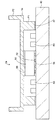
図1(a)は予備的事項に係る放熱板を示す平面図、図1(b)は図1(a)のI−Iに沿った断面斜視図である。図1(a)及び(b)に示すように、予備的事項に係る放熱板100は、平板部120と、平板部120の外周部に上側に突出して配置された突出部140とから形成される。平板部120の外周部に突出部140を配置することによって、半導体チップが収容される収容部Sが設けられている。
FIG. 1 (a) is a plan view showing a heat sink related to preliminary matters, and FIG. 1 (b) is a cross-sectional perspective view taken along the line I-I of FIG. 1 (a). As shown in FIGS. 1A and 1B, the
そして、図2に示すように、半導体チップ200が搭載された配線基板300の上に放熱板100の突出部140が固定される。これにより、放熱板100の収容部Sに半導体チップ200が収容され、半導体チップ200の背面が放熱板100に熱結合される。
Then, as shown in FIG. 2, the
図2の半導体装置の配線基板300は、常温時に凸状に反った状態となっており、熱サイクル試験や実際に半導体装置を使用する際に温度が上がると平坦な状態になる。このように、半導体装置に熱サイクルがかかると、配線基板300の反り状態が変化するため、放熱板100に曲げ応力がかかる。
The
このとき、放熱板100の突出部140の幅Wが2mm程度と小さいため、配線基板300の反り応力に抵抗できず、放熱板100が曲がってしまう。このため、放熱板100の内面と半導体チップ200の背面との密着性が悪くなったり、放熱板100が半導体チップ200から剥がれたりすることがあり、良好な熱結合が得られなくなる。
At this time, since the width W of the
放熱板100の突出部140の幅Wを4mm〜6mm程度に大きくすることにより、配線基板300の反り応力に抵抗できるようになるため、熱サイクルがかかっても放熱板100が曲りにくくなる。
By increasing the width W of the protruding
しかし、突出部140を備えた放熱板100は鍛造技術によって製造されるため、放熱板100の幅Wを大きくすることは困難である。
However, since the
図3及び図4を参照して、放熱板100を鍛造技術により製造する方法を説明する。図3に示すように、上面側に凹部420を備えた下型400と、下面側に凸部520を備えた上型500を用意する。そして、四角形状の金属板110を用意する。下型400の凹部420の平面サイズは金属板110の平面サイズに対応している。
A method of manufacturing the
また、上型500の凸部520の平面サイズは、金属板110の外周部を除く中央部に対応している。
Further, the plane size of the
そして、金属板110を下型400の凹部420に配置し、上型500の凸部520で金属板110の外周部を除く中央部を下側に押圧する。
Then, the
これにより、図4(a)に示すように、押圧されない金属板110の外周部が上側に押し上げられて、上側に突出する突出部140が形成される。このとき、突出部140は、下型400と上型500の間で外側に流動したはみ出し部140aを備えて形成される。
As a result, as shown in FIG. 4A, the outer peripheral portion of the
さらに、図4(b)に示すように、突出部140のはみ出し部140aをポンチで打ち抜いて除去する。これにより、前述した図1(a)及び(b)の突出部140を備えた放熱板100が得られる。
Further, as shown in FIG. 4B, the protruding
上記した図4(a)において、金属板110を上型500の凸部520で押圧して金属板110の外周部を上側に押し上げるにはかなりのプレス荷重をかける必要がある。通常の鍛造技術では、突出部140を形成するための金属板110の外周部の幅は2mm程度が限界である。
In FIG. 4A described above, it is necessary to apply a considerable press load in order to press the
鍛造技術では、成形時に金型が安全に耐えられる最大荷重が決まっており、金型の破損などを防止するため、最大荷重を超えるプレス荷重をかけることはできない。 In the forging technology, the maximum load that the die can safely withstand during molding is determined, and in order to prevent damage to the die, a press load exceeding the maximum load cannot be applied.
また、鍛造技術以外に、薄板の金属板の外周部を曲げ加工によって上側に屈曲させることにより、突出部140を備えた放熱板100を製造する方法がある。このような曲げ加工においても、金属板の厚みは2mm程度が限界であり、放熱板100の突出部140の幅を4mm〜6mm程度に大きくすることは困難である。
In addition to the forging technique, there is a method of manufacturing a
また、鍛造技術及び曲げ加工以外に、金属板の中央部をルータなどで切削加工して凹部を形成することにより、突出部140を備えた放熱板100を製造する方法がある。このような切削加工を使用することにより、放熱板100の突出部140の幅を4mm〜6mm程度に大きくすることは可能である。しかし、切削加工は、一枚の金属板の処理時間が長く、生産効率が悪いため、量産にはコスト面で向かない。
Further, in addition to the forging technique and the bending process, there is a method of manufacturing the
以下に説明する実施形態の放熱板及びその製造方法では、前述した課題を解消することができる。 The above-mentioned problems can be solved by the heat radiating plate and the method for manufacturing the heat radiating plate of the embodiment described below.
本願発明者は、曲げ応力に強い新規な構造の放熱板を鍛造技術によって製造する手法を見出した。 The inventor of the present application has found a method for manufacturing a heat radiating plate having a novel structure resistant to bending stress by a forging technique.
(実施の形態)
図5〜図14は実施形態の放熱板の製造方法を説明するための図、図15〜図20は実施形態の放熱板を説明するための図、図21及び図22は実施形態の電子部品装置を示す図である。以下、放熱板の製造方法を説明しながら、放熱板及び半導体装置の構造について説明する。
(Embodiment)
5 to 14 are views for explaining a method of manufacturing the heat sink of the embodiment, FIGS. 15 to 20 are views for explaining the heat sink of the embodiment, and FIGS. 21 and 22 are electronic components of the embodiment. It is a figure which shows the apparatus. Hereinafter, the structure of the heat radiating plate and the semiconductor device will be described while explaining the method of manufacturing the heat radiating plate.
実施形態の放熱板の製造方法では、図5に示すように、まず、金型として、下型20及び上型30を用意する。下型20は上面側に凹部20aを備えている。また、上型30は下面側に凸部30aを備えている。さらに、平面視で四角形状の金属板10を用意する。
In the method for manufacturing a heat sink of the embodiment, first, as a mold, a
下型20の凹部20aの平面サイズは金属板10の平面サイズに対応している。また、上型30の凸部30aの平面サイズは、金属板10の外周部を除く中央部の平面サイズに設定されている。
The plane size of the
そして、下型20の凹部20aに金属板10を配置する。例えば、金属板10として、銅板又はアルミニウム板などが使用される。また、金属板10の厚みは3mm〜4mm程度であり、金属板10の平面サイズは40mm×40mm〜70mm×70mmである。
Then, the
次いで、図6に示すように、下型20の凹部20a内で金属板10を支持した状態で、上型30の凸部30aで金属板10を下側に押圧する。
Next, as shown in FIG. 6, the
これにより、金属板10の中央部が下側に潰されることで、金属板10の外周部が上側に押し上げられる。金属板10の押し上げられた部分は下型20と上型30との間の空間に沿って外側に流動する。
As a result, the central portion of the
その結果、金属板10の中央部が潰されて厚みが薄くなった平板部10aとなる。また同時に、金属板10の外周部に、平板部10aに繋がって上側に突出する第1突出部P1と、第1突出部P1の上部側面から外側に延びる外延部10bとが形成される。
As a result, the central portion of the
この工程では、金属板10の押し上げられる外周部の幅は2mm程度に設定されるため、通常の鍛造技術により、金属板10を安定して加工することができる。
In this step, since the width of the outer peripheral portion of the
その後に、図7(a)に示すように、図6の加工された金属板10を下型20及び上型30から取り外す。図7(b)は、図7(a)の加工された金属板10を平面からみた平面図である。
After that, as shown in FIG. 7A, the processed
図7(a)及び(b)に示すように、第1突出部P1は四角形状の平板部10aの外周部の上に環状に配置される。また、外延部10bは第1突出部P1の上部側面に環状に繋がって形成される。外延部10bの長さは、例えば、4mm〜6mm程度に設定される。
As shown in FIGS. 7A and 7B, the first protruding portion P1 is arranged in an annular shape on the outer peripheral portion of the rectangular
このようにして、金型によって金属板10を押圧することにより、平板部10aと、平板部10aの外周部に上側に突出して配置された環状の第1突出部P1と、第1突出部P1の上部側面から外側に延びる外延部10bとを形成する。
By pressing the
次いで、図8に示すように、金型として、下型22及び上型32を用意する。下型22は金属板10を支持する平板状の支持部材である。
Next, as shown in FIG. 8, a
上型32は、図7(a)及び(b)の金属板10の外延部10bに対応する環状の凸部32aを備えている。また、上型32は、凸部32aで金属板10の外延部10bを押圧する際に金属板10の第1突出部P1が収容される凹部32bを備えている。
The
そして、図9に示すように、下型22の上に配置された金属板10の外延部10bを上型32の凸部32aで下側に押圧することにより、外延部10bを第1突出部P1の上部側面から下部側面に押し込んで移動させる。このとき、金属板10の第1突出部P1が上型32の凹部32bに収容された状態となる。
Then, as shown in FIG. 9, the
このようにして、金型により、外延部10bを下側に押し込んで移動させることにより、外延部10bを第1突出部P1の下部側面に繋げる。
In this way, the
その後に、図10(a)に示すように、図9の加工された金属板10を下型22及び上型32から取り外す。図10(b)は、図10(a)の加工された金属板10を平面からみた平面図である。図10(a)及び(b)に示すように、外延部10bを第1突出部P1の下部に移動させることにより、平面視で外周が四角形状の第1突出部P1となる。
After that, as shown in FIG. 10A, the processed
外延部10bは、平板部10aの外周部の第1突出部P1の下部側面に環状に繋がって配置される。外延部10bの厚みは平板部10aの厚みよりも薄くなるように加工される。後の工程で、外延部10bを曲げて第2突出部を形成する際に、曲げ加工を容易にするためである。例えば、平板部10aの厚みは2.5mm〜3.5mm程度であり、外延部10bの厚みは1mm〜2mm程度である。
The
次いで、図11に示すように、図10(a)の加工された金属板10を下型24の上に配置し、金属板10の外延部10bの先端部を上型34で打ち抜いて除去する。
Next, as shown in FIG. 11, the processed
このとき、図12の平面図に示すように、金属板10の外延部10bの先端部と共に、平板部10aの四隅の外側領域の外延部10bが上型34により打ち抜かれて除去される。これにより、金属板10の外延部10bの丸みを帯び先端面が平坦面に加工される。また同時に、金属板10の第1突出部P1の四隅の外側領域の外延部10bが除去されて開口部10xが設けられる。
At this time, as shown in the plan view of FIG. 12, the
このようにして、金属板10の外延部10bが四角形状の第1突出部P1の四辺に相互に分離された状態で配置される。
In this way, the
第1突出部P1の四隅の外側領域の外延部10bを除去しておくことにより、次の工程で、金属板10の外延部10bを上側に曲げる際に、曲げ加工が容易になる。
By removing the
次いで、図13に示すように、金型として、下型26及び上型36を用意する。下型26は上面側に凹部26aを備えている。下型26の凹部26aは、図12の加工された金属板10の第1突出部P1を含む四角領域に対応する四角形状で形成される。
Next, as shown in FIG. 13, a
そして、図12の加工された金属板10を下型26の上に配置する。このとき、金属板10の第1突出部P1の四辺に配置された各外延部10bが下型26の凹部26aの周囲の上面に配置された状態となる。また、上型36は平板状の押圧部材である。
Then, the processed
続いて、図14に示すように、図13の金属板10を上型36で下側に押圧する。これにより、外延部10bが下型26の凹部26aの開口端に接した部分で上側に曲げ加工される。
Subsequently, as shown in FIG. 14, the
その結果、水平方向に配置された外延部10bが垂直方向に曲げ加工されて、第1突出部P1に繋がる第2突出部P2となる。第1突出部P1の下部に第2突出部P2の下部が繋がって形成される。第1突出部P1と第2突出部P2とは垂直方向に並んで突出して配置される。また、第1突出部P1と第2突出部P2との間に隙間Cが設けられた状態となる。
As a result, the
このようにして、外延部10bを第1突出部P1の突出方向と同じ方向に曲げることにより、第1突出部P1の外側に第2突出部P2を形成する。
In this way, the
第1突出部P1と第2突出部P2とが接して形成されるようにしてもよい。また、第1突出部P1及び第2突出部P2の各先端面が上型36で押圧されることにより、第1突出部P1の先端面と第2突出部P2の先端面とが同じ高さ位置に配置される。
The first protruding portion P1 and the second protruding portion P2 may be formed in contact with each other. Further, since the tip surfaces of the first protrusion P1 and the second protrusion P2 are pressed by the
このように、通常の鍛造技術により、金属板10の外周部に第1突出部P1と外延部10bを形成し、外延部10bを上側に曲げ加工して補強用の第2突出部P2を容易に形成することができる。
In this way, the first protruding portion P1 and the
その後に、図14の加工された金属板10を下型26及び上型36から取り外す。
After that, the processed
以上により、図15に示すように、実施形態の放熱板1が得られる。図16(a)は実施形態の放熱板を示す平面図、図16(b)は図16(a)のII−IIに沿った斜視断面図である。
As a result, as shown in FIG. 15, the
図15、図16(a)及び(b)に示すように、実施形態の放熱板1は、四角形状の平板部10aと、平板部10aの外周部に平板部10aの厚み方向に突出する第1突出部P1とを備えている。第1突出部P1は、平板部10aの外周部に環状に繋がって形成され、平面視で外周が四角形状となっている。
As shown in FIGS. 15, 16 (a) and 16 (b), the
また、放熱板1は、第1突出部P1の外側に形成された外延部10bと、外延部10bに形成された第2突出部P2とを備えている。第2突出部P2は、第1突出部P1の下部に繋がった状態で、第1突出部P1の突出方向と同じ方向に突出している。このように、平板部10aと第1突出部P1と外延部10bと第2突出部P1とが一体的に形成されている。
Further, the
また、図16(b)に示すように、平板部10aの下面S1と外延部10bの下面S2とが面一で形成されている。第1突出部P1と第2突出部P2との間に隙間C(図15)が設けられている。隙間Cの間隔は、例えば、1mm程度である。
Further, as shown in FIG. 16B, the lower surface S1 of the
隙間Cは、第1突出部P1の外側面SXと、外延部10bの上面SYと、第2突出部P2の内側面SZとで区画された凹状の空間である。あるいは、第1突出部P1と第2突出部P2とが接した状態で形成されていてもよい。
The gap C is a concave space partitioned by the outer surface SX of the first protruding portion P1, the upper surface SY of the
また、図16の部分拡大図に示すように、外延部10bの厚みT2は平板部10aの厚みT1よりも薄く設定されている。さらに、第2突出部P2の厚みW2は、第1突出部P1の厚みW1よりも薄く設定されている。あるいは、第2突出部P2の厚みW2は、第1突出部P1の厚みW1と同じに設定されている。前述したように、外延部10bを曲げて第2突出部P2を形成する際に、曲げ加工を容易にするためである。
Further, as shown in the partially enlarged view of FIG. 16, the thickness T2 of the
また、第1突出部P1の先端面と第2突出部P2の先端面とは同じ高さ位置に配置されている。あるいは、第1突出部P1の先端面が第2突出部P2の先端面よりも突出した位置に配置されてよい。 Further, the tip surface of the first protrusion P1 and the tip surface of the second protrusion P2 are arranged at the same height position. Alternatively, the tip surface of the first protruding portion P1 may be arranged at a position protruding from the tip surface of the second protruding portion P2.
また、図16(a)に示すように、外周が四角形状の第1突出部P1の四隅の外側領域には、第2突出部P2が配置されておらず、第2突出部P2の開口部10xが設けられている。このように、第2突出部P2は、第1突出部P1の四辺に相互に分離された状態で配置されている。 Further, as shown in FIG. 16A, the second protrusion P2 is not arranged in the outer regions of the four corners of the first protrusion P1 having a quadrangular outer circumference, and the opening of the second protrusion P2. 10x is provided. In this way, the second protruding portion P2 is arranged on the four sides of the first protruding portion P1 in a state of being separated from each other.
図16(b)に示すように、平板部10aとその外周部に配置された第1突出部P1とによって電子部品が収容される収容部Sが設けられている。
As shown in FIG. 16B, an accommodating portion S in which electronic components are accommodated is provided by a
金属板10の第1突出部P1及び第2突出部P2が配線基板に固定される脚部として機能し、第1突出部P1及び第2突出部P2の各先端面が配線基板に固定される。
The first protruding portion P1 and the second protruding portion P2 of the
本実施形態の放熱板1では、平板部10aの外周部に第1突出部P1が配置され、第1突出部P2の外側に補強用の第2突出部P2が配置されている。
In the
このように、放熱板1の第1突出部P1の外側に第2突出部P2を並べて配置することにより、放熱板1の脚部の幅を実質的に大きくすることができる。このため、放熱板に曲げ応力がかかっても、放熱板が曲りにくくなる。
By arranging the second protruding portions P2 side by side on the outside of the first protruding portion P1 of the
例えば、第1突出部P1の幅W1は2mm程度であり、第2突出部P2の幅W2は1mm〜2mm程度である。この場合、第1突出部P1及び第2突出部P2のトータルの幅は、隙間Cを含めて4mm〜5mm程度に大きくなる。 For example, the width W1 of the first protruding portion P1 is about 2 mm, and the width W2 of the second protruding portion P2 is about 1 mm to 2 mm. In this case, the total width of the first protruding portion P1 and the second protruding portion P2 is as large as about 4 mm to 5 mm including the gap C.
また、通常の鍛造技術により、金属板10の外周部に第1突出部P1とそれに繋がる外延部10bを形成し、外延部10bを上側に曲げることにより、第1突出部P1の外側に補強用の第2突出部P2を容易に形成することができる。
Further, by forming a first protruding portion P1 and an outer extending
よって、特別な製造設備や製造方法を導入する必要がないため、コスト上昇を招くことなく、曲げ強度の強い放熱板を信頼性よく製造することができる。 Therefore, since it is not necessary to introduce special manufacturing equipment or manufacturing method, it is possible to reliably manufacture a heat sink having strong bending strength without causing an increase in cost.
次に、実施形態の変形例の放熱板について説明する。図17は実施形態の変形例の放熱板を示す断面図である。図18(a)は実施形態の変形例の放熱板を示す平面図、図18(b)は図18(a)のIII−IIIに沿った断面斜視図である。 Next, the heat sink of the modified example of the embodiment will be described. FIG. 17 is a cross-sectional view showing a heat sink of a modified example of the embodiment. FIG. 18A is a plan view showing a heat sink of a modified example of the embodiment, and FIG. 18B is a cross-sectional perspective view along III-III of FIG. 18A.
図17、図18(a)及び(b)に示すように、変形例の放熱板1aでは、前述した図15、図16(a)及び(b)の放熱板1の第2突出部P2が、第1突出部P1の突出方向と逆方向に突出する第2突出部P2xとなっている。
As shown in FIGS. 17, 18 (a) and 18 (b), in the
図17、図18(a)及び(b)において、第2突出部P2x以外の要素は、15、図16(a)及び(b)の放熱板1と同じである。
In FIGS. 17, 18 (a) and 18 (b), the elements other than the second protruding portion P2x are the same as those in the
図18(a)に示すように、変形例の放熱板1aにおいても、前述した図16(a)の放熱板1と同様に、外周が四角形状の第1突出部P1の四隅の外側領域には、第2突出部P2xは配置されておらず、第2突出部P2xの開口部10xが設けられている。
As shown in FIG. 18A, also in the
変形例の放熱板1aを製造する際には、前述した図13及び図14の工程で、別の金型を使用して金属板10の外延部10bを第1突出部P1の突出方向と逆方向に曲げる。
When manufacturing the
図19に示すように、前述した図13の金属板10と、金型として下型28及び上型38を用意する。下型28は上面側に凹部28aを備えている。また、上型38は下面側に凸部38aを備えている。
As shown in FIG. 19, the
そして、金属板10の第1突出部P1を下型28の凹部28aに配置した状態で、金属板10の外延部10bを下型28の凹部28aの周囲の上面に配置する。さらに、上型38の凸部38aで金属板10を下側に押圧する
これにより、図20に示すように、外延部10bが下型28の凹部28aの開口端に接した部分で上側に曲げ加工される。このようにして、外延部10bを第1突出部P1の突出方向と逆方向に曲げることより、第1突出部P1の反対側に第2突出部P2xを形成する。
Then, in a state where the first protruding portion P1 of the
図18(b)に示すように、変形例の放熱板1aでは、第1突出部P1の外側に形成された外延部10bの上面SAが第1突出部P1の外周に露出している。また、第1突出部P1の外周には、第1突出部P1の外側面SBと、外延部10bの上面SAとからなる段差Dが形成されている。
As shown in FIG. 18B, in the
また、図18(b)の部分拡大図に示された変形例の放熱板1aの各厚みT1,T2,W1,W2は、前述した図16(b)の放熱板1と同じ構成を適用することができる。
Further, the thicknesses T1, T2, W1 and W2 of the
変形例の放熱板1aでは、第1突出部P1が配線基板に固定される脚部として機能する。そして、第1突出部P1の外側上部に、第1突出部P1の突出方向と逆方向に突出する第2突出部P2xが配置されている。
In the
このように、変形例の放熱板1aでは、第1突出部P1(脚部)の四辺の上方に壁状の第2突出部P2xが立設しているため、第2突出部P2xによって放熱板1aの曲げ強度が補強される。このため、放熱板1aに曲げ応力がかかっても、放熱板1aが曲りにくくなる。
As described above, in the
また、前述した図16(a)及び(b)の放熱板1と同様に、通常の鍛造技術によって金属板10を加工することにより、第1突出部P1の外側に補強用の第2突出部P2xを容易に形成することができる。
Further, similarly to the
次に、図15、図16(a)及び(b)の実施形態の放熱板1を電子部品装置に適用する方法について説明する。図21に示すように、配線基板40を用意する。配線基板40の両面側には配線層(不図示)が形成されており、両面側の配線層は内部に形成されたビアを含む多層配線層(不図示)を介して相互接続されている。
Next, a method of applying the
さらに、下面側に接続端子52を備えた半導体チップ50を用意する。そして、半導体チップ50の接続端子52を配線基板40の上面側の配線層のパッドにフリップチップ接続する。その後に、半導体チップ50の下側の隙間にアンダーフィル樹脂54を充填する。半導体チップ50は、例えば、発熱量が大きいCPUチップなどである。
Further, a
さらに、半導体チップ50の周囲の配線基板40の上に、キャパシタ素子60を搭載する。キャパシタ素子60の他に、コントローラチップやメモリチップなどを搭載してもよい。
Further, the
半導体チップ50及びキャパシタ素子60などは電子部品の一例であり、各種の電子部品を使用することができる。このようにして、配線基板40の上に各種の電子部品が搭載される。
The
さらに、前述した図15(a)の放熱板1を用意する。そして、放熱板1の第1突出部P1及び第2突出部P2の先端面を配線基板40の上に接着剤42で接着して固定する。
Further, the
このとき同時に、半導体チップ50の背面が熱伝導材56によって放熱板1の平板部10aの内面に接続されて熱結合される。熱伝導材56としては、インジウムシート、シリコーングリース、又はカーボンナノチューブシートなどが使用される。
At the same time, the back surface of the
また、放熱板1の第1突出部P1と第2突出部P2との間に隙間Cが設けられているため、接着剤42が隙間Cに充填される。これにより、放熱板1の接着面積が大きくなるため、放熱板1の接着強度を向上させることができる。
Further, since the gap C is provided between the first protruding portion P1 and the second protruding portion P2 of the
以上により、実施形態の電子部品装置2が製造される。予備的事項で説明したように、図21の電子部品装置2の配線基板40は、常温時に凸状に反った状態となっており、熱サイクル試験や実際に半導体装置を使用する際に温度が上がると平坦な状態になる。このように、電子部品装置2に熱サイクルがかかると、配線基板40の反り状態が変化するため、放熱板1に曲げ応力がかかる。
As described above, the
電子部品装置2の放熱板1では、前述したように、配線基板40に固定される放熱板1の脚部が第1突出部P1と補強用の第2突出部P2とから形成される。このため、放熱板1の脚部の幅が実質的に大きくなるため、放熱板1の曲げ強度が補強される。
In the
よって、熱サイクルによって配線基板40の反り状態が変化することで放熱板1に曲げ応力がかかっても、放熱板1が曲りにくくなる。これにより、放熱板1の内面と半導体チップ50の背面との密着性が悪くなったり、放熱板1が半導体チップ50から剥がれたりすることが防止される。
Therefore, even if bending stress is applied to the
このように、実施形態の電子部品装置2では、半導体チップ50から発する熱を熱伝導材56を介して放熱板1に良好に放熱することができ、電子部品装置2の信頼性を向上させることができる。
As described above, in the
図22には、実施形態の変形例の電子部品装置2aが示されている。図22に示す変形例の電子部品装置2aでは、前述した図21の電子部品装置2の放熱板1の代わりに図17の変形例の放熱板1aを使用している。図22において、放熱板1a以外の要素は図21の電子部品装置2と同一であるため、同一符号を付してそれらの説明を省略する。
FIG. 22 shows an
図22に示すように、変形例の電子部品装置2aでは、放熱板1aの平板部10aの外周部から下側に突出する第1突出部P1が配置されている。さらに、第1突出部P1の外側上部に、上側に突出する第2突出部P2xが繋がって形成されている。
As shown in FIG. 22, in the
このように、配線基板40に固定される放熱板1aの第1突出部P1(脚部)の四辺の上方に壁状の第2突出部P2xが立設しているため、第2突出部P2xによって放熱板1aの曲げ強度が補強される。
In this way, since the wall-shaped second protruding portion P2x is erected above the four sides of the first protruding portion P1 (leg portion) of the
よって、図21の電子部品装置2と同様に、電子部品装置2aの配線基板40の反り状態が変化しても放熱板1aが曲りにくくなり、半導体チップ50から発する熱を放熱板1aに良好に放熱することができる。
Therefore, similarly to the
1,1a…放熱板、2,2a…電子部品装置、10…金属板、10a…平板部、10b…外延部、10x…開口部、20,22,24,26,28…下型、20a,26a,32b,26a,28a…凹部、30,32,34,36,38…上型、30a,32a,38a…凸部、40…配線基板、42…接着剤、50…半導体チップ、52…接続端子、54…アンダーフィル樹脂、56…熱伝導材、C…隙間、P1…第1突出部、P2,P2x…第2突出部。 1, 1a ... radiator plate, 2, 2a ... electronic component device, 10 ... metal plate, 10a ... flat plate portion, 10b ... extension unit, 10x ... opening, 20, 22, 24, 26, 2 8 ... lower mold, 20a , 26a, 32b, 26a, 28a ... concave, 30, 32, 34, 36, 38 ... upper mold, 30a, 32a, 38a ... convex, 40 ... wiring board, 42 ... adhesive, 50 ... semiconductor chip, 52 ... Connection terminal, 54 ... underfill resin, 56 ... heat conductive material, C ... gap, P1 ... first protruding portion, P2, P2x ... second protruding portion.
Claims (10)
前記平板部の外周部に形成され、前記平板部の厚み方向に突出する環状の第1突出部と、
前記第1突出部の外側に形成された外延部と、
前記外延部に形成され、前記第1突出部と同じ方向又は逆方向のいずれかに突出する第2突出部と
を有し、
前記第1突出部は外周が四角形状であり、
前記第1突出部の四隅の外側領域に前記第2突出部の開口部が設けられており、
前記外延部の厚みは、前記平板部の厚みよりも薄いことを特徴とする放熱板。 Flat plate and
An annular first protruding portion formed on the outer peripheral portion of the flat plate portion and projecting in the thickness direction of the flat plate portion,
An extension portion formed on the outside of the first protrusion and
It has a second protrusion that is formed on the extension and projects in either the same direction as or in the opposite direction to the first protrusion.
The first protruding portion has a quadrangular outer circumference and has a quadrangular outer circumference.
The openings of the second protrusion are provided in the outer regions of the four corners of the first protrusion .
A heat radiating plate characterized in that the thickness of the extension portion is thinner than the thickness of the flat plate portion.
前記第1突出部と前記第2突出部との間に隙間が設けられていることを特徴とする請求項1に記載の放熱板。 The second protruding portion protrudes in the same direction as the first protruding portion.
The heat radiating plate according to claim 1, wherein a gap is provided between the first protruding portion and the second protruding portion.
前記第1突出部の先端面と前記第2突出部の先端面とは同じ高さ位置に配置されていることを特徴とする請求項1又は2に記載の放熱板。 The second protruding portion protrudes in the same direction as the first protruding portion.
The heat radiating plate according to claim 1 or 2 , wherein the tip surface of the first protrusion and the tip surface of the second protrusion are arranged at the same height position.
前記配線基板の上に搭載された電子部品と、
請求項1乃至4のいずれか1項に記載の放熱板と
を有し、
前記放熱板の第1突出部が前記配線基板の上に配置されて、前記放熱板の中に前記電子部品が収容され、
前記放熱板と前記電子部品とが熱伝導材で接続されていることを特徴とする電子部品装置。 Wiring board and
Electronic components mounted on the wiring board and
The heat sink according to any one of claims 1 to 4 is provided.
The first protruding portion of the heat sink is arranged on the wiring board, and the electronic component is housed in the heat sink.
An electronic component device characterized in that the heat radiating plate and the electronic component are connected by a heat conductive material.
金型によって前記金属板を押圧することにより、平板部と、前記平板部の外周部に上側に突出して配置された第1突出部と、第1突出部の上部側面から外側に延びる外延部とを形成する工程と、
金型によって前記外延部を下側に押し込んで移動させることにより、前記外延部を前記第1突出部の下部側面に繋げる工程と、
前記外延部を前記第1突出部の突出方向と同じ方向又は逆方向のいずれかに曲げることにより、前記第1突出部の外側に第2突出部を形成する工程と
を有することを特徴とする放熱板の製造方法。 The process of preparing the metal plate and
By pressing the metal plate with a mold, a flat plate portion, a first protruding portion arranged so as to project upward on the outer peripheral portion of the flat plate portion, and an outer extension portion extending outward from the upper side surface of the first protruding portion. And the process of forming
A step of connecting the extension portion to the lower side surface of the first protrusion portion by pushing the extension portion downward by a mold and moving the extension portion.
It is characterized by having a step of forming a second protruding portion on the outside of the first protruding portion by bending the outer extension portion in either the same direction as or opposite to the protruding direction of the first protruding portion. How to manufacture a heat sink.
前記外延部を前記第1突出部の突出方向と同じ方向に曲げて前記第2突出部を形成し、
前記第1突出部と前記第2突出部との間に隙間が設けられることを特徴とする請求項6に記載の放熱板の製造方法。 In the step of forming the second protrusion,
The extension portion is bent in the same direction as the protrusion direction of the first protrusion to form the second protrusion.
The method for manufacturing a heat radiating plate according to claim 6, wherein a gap is provided between the first protruding portion and the second protruding portion.
前記第1突出部の外周は四角形状で形成され、
前記外延部を前記第1突出部の下部側面に繋げる工程の後であって、前記第2突出部を形成する工程の前に、
前記外延部の先端部を除去すると共に、前記第1突出部の四隅の外側領域の前記外延部を除去して開口部を設ける工程を有することを特徴とする請求項6又は7に記載の放熱板の製造方法。 In the step of forming the flat plate portion, the first protruding portion, and the extension portion,
The outer circumference of the first protrusion is formed in a quadrangular shape.
After the step of connecting the extension portion to the lower side surface of the first protrusion portion, and before the step of forming the second protrusion portion,
The heat dissipation according to claim 6 or 7, further comprising a step of removing the tip portion of the extension portion and removing the extension portion in the outer region of the four corners of the first protrusion to provide an opening. How to make a board.
前記外延部の厚みは前記平板部の厚みよりも薄く設定されることを特徴とする請求項6乃至8のいずれか一項に記載の放熱板の製造方法。 In the step of forming the flat plate portion, the first protruding portion, and the extension portion,
The method for manufacturing a heat radiating plate according to any one of claims 6 to 8, wherein the thickness of the extension portion is set to be thinner than the thickness of the flat plate portion.
前記外延部を前記第1突出部の突出方向と同じ方向に曲げて前記第2突出部を形成し、
前記第1突出部の先端面と前記第2突出部の先端面とが同じ高さ位置に配置されることを特徴とする請求項6乃至9のいずれか一項に記載の放熱板の製造方法。 In the step of forming the second protrusion,
The extension portion is bent in the same direction as the protrusion direction of the first protrusion to form the second protrusion.
The method for manufacturing a heat radiating plate according to any one of claims 6 to 9, wherein the tip surface of the first protrusion and the tip surface of the second protrusion are arranged at the same height position. ..
Priority Applications (2)
| Application Number | Priority Date | Filing Date | Title |
|---|---|---|---|
| JP2017123920A JP6867243B2 (en) | 2017-06-26 | 2017-06-26 | Heat sink and its manufacturing method and electronic component equipment |
| US15/987,390 US10461013B2 (en) | 2017-06-26 | 2018-05-23 | Heat sink and electronic component device |
Applications Claiming Priority (1)
| Application Number | Priority Date | Filing Date | Title |
|---|---|---|---|
| JP2017123920A JP6867243B2 (en) | 2017-06-26 | 2017-06-26 | Heat sink and its manufacturing method and electronic component equipment |
Publications (3)
| Publication Number | Publication Date |
|---|---|
| JP2019009292A JP2019009292A (en) | 2019-01-17 |
| JP2019009292A5 JP2019009292A5 (en) | 2020-02-27 |
| JP6867243B2 true JP6867243B2 (en) | 2021-04-28 |
Family
ID=64692745
Family Applications (1)
| Application Number | Title | Priority Date | Filing Date |
|---|---|---|---|
| JP2017123920A Active JP6867243B2 (en) | 2017-06-26 | 2017-06-26 | Heat sink and its manufacturing method and electronic component equipment |
Country Status (2)
| Country | Link |
|---|---|
| US (1) | US10461013B2 (en) |
| JP (1) | JP6867243B2 (en) |
Families Citing this family (3)
| Publication number | Priority date | Publication date | Assignee | Title |
|---|---|---|---|---|
| US10510595B2 (en) | 2018-04-30 | 2019-12-17 | Taiwan Semiconductor Manufacturing Company, Ltd. | Integrated fan-out packages and methods of forming the same |
| US20210035921A1 (en) * | 2019-07-30 | 2021-02-04 | Intel Corporation | Soldered metallic reservoirs for enhanced transient and steady-state thermal performance |
| JP2023183142A (en) * | 2022-06-15 | 2023-12-27 | キオクシア株式会社 | Semiconductor device and semiconductor device manufacturing method |
Family Cites Families (17)
| Publication number | Priority date | Publication date | Assignee | Title |
|---|---|---|---|---|
| US5151777A (en) * | 1989-03-03 | 1992-09-29 | Delco Electronics Corporation | Interface device for thermally coupling an integrated circuit to a heat sink |
| JPH0531248A (en) | 1991-08-02 | 1993-02-09 | Sophia Co Ltd | Game machine |
| JPH0531248U (en) * | 1991-09-30 | 1993-04-23 | シヤープ株式会社 | Resin-sealed power semiconductor device |
| JP3313009B2 (en) | 1995-05-19 | 2002-08-12 | 新光電気工業株式会社 | Heat dissipation member, lead frame and semiconductor device |
| JPH11112169A (en) | 1997-10-06 | 1999-04-23 | Nippon Light Metal Co Ltd | Heat sink for integrated circuit module and method of manufacturing the same |
| JP2001338999A (en) * | 2000-05-30 | 2001-12-07 | Kyocera Corp | Package for storing semiconductor elements |
| US20030131476A1 (en) * | 2001-09-28 | 2003-07-17 | Vlad Ocher | Heat conduits and terminal radiator for microcircuit packaging and manufacturing process |
| JP2003277853A (en) * | 2002-03-26 | 2003-10-02 | Dowa Mining Co Ltd | Copper alloy for heat spreader |
| JP2005012127A (en) * | 2003-06-20 | 2005-01-13 | Denso Corp | Electronic control device |
| JP4910439B2 (en) * | 2006-03-23 | 2012-04-04 | 富士通セミコンダクター株式会社 | Semiconductor device |
| JP5733893B2 (en) * | 2009-12-22 | 2015-06-10 | 新光電気工業株式会社 | Electronic component equipment |
| JP5368377B2 (en) * | 2010-06-02 | 2013-12-18 | 三菱電機株式会社 | Electronic component package and manufacturing method thereof |
| JP5719566B2 (en) | 2010-11-04 | 2015-05-20 | 新光電気工業株式会社 | IC package heat sink and IC package connection device having heat sink |
| JP5898919B2 (en) * | 2011-10-31 | 2016-04-06 | 新光電気工業株式会社 | Semiconductor device |
| JP6007535B2 (en) * | 2012-03-22 | 2016-10-12 | 日本電気株式会社 | Hollow sealing structure and hollow package including the same |
| US9524917B2 (en) * | 2014-04-23 | 2016-12-20 | Optiz, Inc. | Chip level heat dissipation using silicon |
| JP6421050B2 (en) * | 2015-02-09 | 2018-11-07 | 株式会社ジェイデバイス | Semiconductor device |
-
2017
- 2017-06-26 JP JP2017123920A patent/JP6867243B2/en active Active
-
2018
- 2018-05-23 US US15/987,390 patent/US10461013B2/en active Active
Also Published As
| Publication number | Publication date |
|---|---|
| US20180374773A1 (en) | 2018-12-27 |
| JP2019009292A (en) | 2019-01-17 |
| US10461013B2 (en) | 2019-10-29 |
Similar Documents
| Publication | Publication Date | Title |
|---|---|---|
| TWI614851B (en) | Electronic package including multilayer reinforcement | |
| CN110024119B (en) | Semiconductor device and manufacturing method thereof | |
| CN101547586B (en) | Heat sink, heat sink combination and fixing device thereof | |
| JP6867243B2 (en) | Heat sink and its manufacturing method and electronic component equipment | |
| CN101621905A (en) | Radiator buckle and radiating device using buckle | |
| US8553417B2 (en) | Heat-radiating substrate and method of manufacturing the same | |
| CN101547584B (en) | Heat sink, heat sink combination and fixing device thereof | |
| US10325829B2 (en) | TIM strain mitigation in electronic modules | |
| CN204217301U (en) | Heat dissipation structure and electronic equipment having the heat dissipation structure | |
| US8269343B2 (en) | Semiconductor device including a pressure-contact section | |
| CN201298543Y (en) | Fixing mould of lapping and packaging piece | |
| US9138840B2 (en) | Method for manufacturing a heat sink | |
| JP2019009292A5 (en) | ||
| KR101089649B1 (en) | Metal laminated plate and core board manufacturing method using the same | |
| JP6734594B2 (en) | Heat sink, method for manufacturing the heat sink, and electronic component package using the heat sink | |
| KR100730626B1 (en) | Method of fabricating substrate for package of semiconductor light-emitting device | |
| JP7152544B2 (en) | Semiconductor heat dissipation package structure | |
| JP7386435B2 (en) | Wiring board and its manufacturing method | |
| JP5256177B2 (en) | Semiconductor package | |
| JP2011166096A (en) | Surface-mounted device and printed board, and structure for mounting surface-mounted device using them | |
| CN104271693B (en) | Thermal pad | |
| CN105458100A (en) | Combination method of heat dissipation aluminum box and heat dissipation parts | |
| CN100403526C (en) | Heat dissipation structure of semiconductor device and semiconductor package | |
| JP5882132B2 (en) | Flexible circuit board and manufacturing method thereof | |
| US20050162827A1 (en) | Heat-dissipating device |
Legal Events
| Date | Code | Title | Description |
|---|---|---|---|
| RD03 | Notification of appointment of power of attorney |
Free format text: JAPANESE INTERMEDIATE CODE: A7423 Effective date: 20180320 |
|
| A521 | Request for written amendment filed |
Free format text: JAPANESE INTERMEDIATE CODE: A523 Effective date: 20200110 |
|
| A621 | Written request for application examination |
Free format text: JAPANESE INTERMEDIATE CODE: A621 Effective date: 20200110 |
|
| A131 | Notification of reasons for refusal |
Free format text: JAPANESE INTERMEDIATE CODE: A131 Effective date: 20201124 |
|
| A977 | Report on retrieval |
Free format text: JAPANESE INTERMEDIATE CODE: A971007 Effective date: 20201126 |
|
| A521 | Request for written amendment filed |
Free format text: JAPANESE INTERMEDIATE CODE: A523 Effective date: 20210114 |
|
| TRDD | Decision of grant or rejection written | ||
| A01 | Written decision to grant a patent or to grant a registration (utility model) |
Free format text: JAPANESE INTERMEDIATE CODE: A01 Effective date: 20210323 |
|
| A61 | First payment of annual fees (during grant procedure) |
Free format text: JAPANESE INTERMEDIATE CODE: A61 Effective date: 20210408 |
|
| R150 | Certificate of patent or registration of utility model |
Ref document number: 6867243 Country of ref document: JP Free format text: JAPANESE INTERMEDIATE CODE: R150 |