JP6851813B2 - Wiring board - Google Patents
Wiring board Download PDFInfo
- Publication number
- JP6851813B2 JP6851813B2 JP2016249490A JP2016249490A JP6851813B2 JP 6851813 B2 JP6851813 B2 JP 6851813B2 JP 2016249490 A JP2016249490 A JP 2016249490A JP 2016249490 A JP2016249490 A JP 2016249490A JP 6851813 B2 JP6851813 B2 JP 6851813B2
- Authority
- JP
- Japan
- Prior art keywords
- resin
- circuit pattern
- wiring board
- metal foil
- meandering
- Prior art date
- Legal status (The legal status is an assumption and is not a legal conclusion. Google has not performed a legal analysis and makes no representation as to the accuracy of the status listed.)
- Active
Links
Images


Classifications
-
- H—ELECTRICITY
- H05—ELECTRIC TECHNIQUES NOT OTHERWISE PROVIDED FOR
- H05K—PRINTED CIRCUITS; CASINGS OR CONSTRUCTIONAL DETAILS OF ELECTRIC APPARATUS; MANUFACTURE OF ASSEMBLAGES OF ELECTRICAL COMPONENTS
- H05K1/00—Printed circuits
- H05K1/02—Details
- H05K1/11—Printed elements for providing electric connections to or between printed circuits
- H05K1/118—Printed elements for providing electric connections to or between printed circuits specially for flexible printed circuits, e.g. using folded portions
-
- H—ELECTRICITY
- H05—ELECTRIC TECHNIQUES NOT OTHERWISE PROVIDED FOR
- H05K—PRINTED CIRCUITS; CASINGS OR CONSTRUCTIONAL DETAILS OF ELECTRIC APPARATUS; MANUFACTURE OF ASSEMBLAGES OF ELECTRICAL COMPONENTS
- H05K3/00—Apparatus or processes for manufacturing printed circuits
- H05K3/38—Improvement of the adhesion between the insulating substrate and the metal
-
- H—ELECTRICITY
- H05—ELECTRIC TECHNIQUES NOT OTHERWISE PROVIDED FOR
- H05K—PRINTED CIRCUITS; CASINGS OR CONSTRUCTIONAL DETAILS OF ELECTRIC APPARATUS; MANUFACTURE OF ASSEMBLAGES OF ELECTRICAL COMPONENTS
- H05K2201/00—Indexing scheme relating to printed circuits covered by H05K1/00
- H05K2201/09—Shape and layout
- H05K2201/09209—Shape and layout details of conductors
- H05K2201/09218—Conductive traces
- H05K2201/09263—Meander
Landscapes
- Engineering & Computer Science (AREA)
- Microelectronics & Electronic Packaging (AREA)
- Manufacturing & Machinery (AREA)
- Structure Of Printed Boards (AREA)
- Laminated Bodies (AREA)
Description
本発明は、配線基板、特に金属箔の回路パターンを備えた配線基板等に関する。また、当該配線基板を用いた構造物等に関する。 The present invention relates to a wiring board, particularly a wiring board provided with a metal foil circuit pattern. It also relates to a structure or the like using the wiring board.
近年、各種電子部品の小型化、組み立ての省力化が進められる中で、三次元形状をもつ導電性回路つき樹脂成型品が求められている。このような構造物を得る方法として、フレキシブルプリント配線基板をインサート品として一体成型するもの(例えば、特許文献1)や樹脂成型品に対して、めっきにより導電性回路を形成するもの(例えば、特許文献2)が挙げられる。 In recent years, with the progress of miniaturization and labor saving of assembly of various electronic parts, a resin molded product having a three-dimensional shape and having a conductive circuit is required. As a method for obtaining such a structure, a flexible printed wiring board is integrally molded as an insert product (for example, Patent Document 1) or a resin molded product is plated to form a conductive circuit (for example, a patent). Reference 2) can be mentioned.
ただ、金属箔の伸び率は厚みにも依存するが、大きくとも30%程度しかない一方、樹脂製フィルムの伸び率は数百%に及び、両者の成形性には大きな開きがある。その為、上記特許文献1の技術によって製造される、金属箔からなる回路が形成された樹脂製フィルムを、起伏が多い成型品に用いると、金属箔が樹脂製フィルムの成型を阻害し、期待したとおりの形状に成型されなかったり、また、回路が成型の際の伸びに追従できず断線してしまう。
However, the elongation rate of the metal foil depends on the thickness, but it is only about 30% at the maximum, while the elongation rate of the resin film reaches several hundred percent, and there is a large difference in moldability between the two. Therefore, when a resin film having a circuit made of a metal foil formed by the technique of
また、特許文献2の技術では、めっきで導電性回路を形成するため、回路厚みを厚くすることが困難であり、また、電気抵抗を下げる為には配線を太くする必要があるために配線の取り回しが困難になる。よって、大電流を流す必要がある製品へは適用が困難である。 Further, in the technique of Patent Document 2, since a conductive circuit is formed by plating, it is difficult to increase the circuit thickness, and it is necessary to increase the wiring in order to reduce the electric resistance. It becomes difficult to handle. Therefore, it is difficult to apply it to products that require a large current to flow.
本発明は、大電流を流すことが可能であり、且つ成型による変形によっても回路の断線や剥離が起こりづらい配線基板を提供することを課題とする。 An object of the present invention is to provide a wiring board capable of passing a large current and in which disconnection or peeling of a circuit is unlikely to occur even due to deformation due to molding.
本発明者らは、金属箔からなる蛇行回路パターンを備えた配線基板であれば、成型による変形によっても回路の断線が抑制されることを見出し、さらに改良を重ねて本発明を完成させるに至った。 The present inventors have found that if a wiring board has a meandering circuit pattern made of metal foil, the disconnection of the circuit can be suppressed even by deformation due to molding, and further improvements have been made to complete the present invention. It was.
本発明は例えば以下の項に記載の主題を包含する。
項1.
樹脂基板の少なくとも片面に金属箔からなる回路パターンを備えた配線基板であって、
前記回路パターンの一部又は全部が、線状の金属箔ラインが長手方向につづら折り状に折り畳まれた構造を有する、つづら折り状の蛇行回路パターンであり、
前記蛇行回路パターンの長手方向のA[mm]の範囲における当該蛇行回路パターンの金属箔ライン長をB[mm]とし、
当該蛇行回路パターンの長手方向における前記樹脂基板の引張破断伸び率をE(resin)[%]、前記金属箔の引張破断伸び率をE(metal)[%]とし、
当該金属箔の常温での0.2%耐力をF[N/mm2]、厚みをT[μm]としたとき、
以下の式(1)と式(2)を満たす、配線基板。
式(1): E(resin)/4−E(metal)<(B−A)/A×100
式(2): (F×T)≦22000
項2.
前記金属箔が、アルミニウム箔又は銅箔である、項1に記載の配線基板。
項3.
前記樹脂基板が、ポリエチレン系樹脂、ポリプロピレン系樹脂、ポリエステル系樹脂、アクリル系樹脂、及びポリカーボネート系樹脂からなる群より選択される少なくとも1種の樹脂を含む基板である、項1または2に記載の配線基板。
項4.
前記金属箔の少なくとも一部が保護用樹脂で被覆されている、項1〜3のいずれかに記載の配線基板。
項5.
前記金属箔が、接着層を介して前記樹脂基板の少なくとも一方の表面に積層されている、項1〜4のいずれかに記載の配線基板。
項6.
前記蛇行回路パターンの長手方向へ、つづら折り状の蛇行回路が引き延ばされる力が加わる成型用である、項1〜5のいずれかに記載の配線基板。
項7.
項1〜6のいずれかに記載の配線基板の成型加工物。
項8.
項1〜6のいずれかに記載の配線基板又は項7に記載の成型加工物を備える、構成物。
The present invention includes, for example, the subjects described in the following sections.
A wiring board having a circuit pattern made of metal foil on at least one side of a resin board.
A part or all of the circuit pattern is a zigzag meandering circuit pattern having a structure in which linear metal leaf lines are folded in a zigzag shape in the longitudinal direction.
The metal leaf line length of the meandering circuit pattern in the range of A [mm] in the longitudinal direction of the meandering circuit pattern is defined as B [mm].
The tensile elongation at break of the resin substrate in the longitudinal direction of the meandering circuit pattern is E (resin) [%], and the elongation at tensile elongation of the metal foil is E (metal) [%].
When the 0.2% proof stress of the metal foil at room temperature is F [N / mm 2 ] and the thickness is T [μm].
A wiring board that satisfies the following equations (1) and (2).
Equation (1): E (resin) / 4-E (metal) <(BA) / A × 100
Equation (2): (F × T) ≦ 22000
Item 2.
Item 2. The wiring board according to
Item 3.
Item 2. The
Item 4.
Item 2. The wiring board according to any one of
Item 5.
Item 2. The wiring board according to any one of
Item 6.
Item 2. The wiring board according to any one of
Item 7.
Item 7. A molded processed product of a wiring board according to any one of
Item 8.
A component comprising the wiring board according to any one of
上記の配線基板であれば、回路が金属箔であるために大電流を流すことが可能であり、且つ上記の構成を有することによって、成型の際に回路が樹脂の伸びに追従できず断線してしまったり、回路が樹脂基板から剥離してしまうことを低減することができる。 With the above wiring board, since the circuit is made of metal foil, it is possible to pass a large current, and by having the above configuration, the circuit cannot follow the elongation of the resin during molding and is disconnected. It is possible to reduce the possibility that the circuit will be peeled off from the resin substrate.
以下、本発明の各実施形態について、さらに詳細に説明する。 Hereinafter, each embodiment of the present invention will be described in more detail.
本発明に包含される配線基板は、樹脂基板の少なくとも片面(片面又は両面)に金属箔からなる回路パターンを備えた配線基板である。 The wiring board included in the present invention is a wiring board having a circuit pattern made of a metal foil on at least one side (one side or both sides) of the resin board.
当該樹脂基板は、樹脂を含有する基板である。その形状は特に制限されず、成型により変形しやすいもの(フレキシブル基板)であることが好ましい。例えば、シート状、フィルム状の樹脂基板を好ましく用いることができる。樹脂基板の厚みは、本発明の効果が損なわれない範囲であれば特に制限されないが、例えば20〜300μmが好ましく、40〜200μmがより好ましく、50〜150μmがさらに好ましい。樹脂基板が薄すぎると当該基板を用いて製造した成型加工物の強度が低くなるおそれがある。また、逆に厚すぎると成型性に支障が出たり、コストアップに繋がる。 The resin substrate is a substrate containing a resin. The shape is not particularly limited, and it is preferable that the shape is easily deformed by molding (flexible substrate). For example, a sheet-shaped or film-shaped resin substrate can be preferably used. The thickness of the resin substrate is not particularly limited as long as the effects of the present invention are not impaired, but for example, it is preferably 20 to 300 μm, more preferably 40 to 200 μm, and even more preferably 50 to 150 μm. If the resin substrate is too thin, the strength of the molded product manufactured using the substrate may decrease. On the other hand, if it is too thick, the moldability will be hindered and the cost will increase.
樹脂基板に含有される樹脂は特に制限されないが、例えば、ポリエチレン系樹脂、ポリプロピレン系樹脂、ポリエステル系樹脂、ポリアミド(ナイロン)系樹脂、アクリル系樹脂、ポリ塩化ビニル系樹脂、ポリスチレン系樹脂、ポリ塩化ビニリデン系樹脂、エチレン−酢酸ビニル共重合体ケン化物、ポリビニルアルコール系樹脂、ポリカーボネート系樹脂、ポリ酢酸ビニル系樹脂、アセタール系樹脂等が挙げられる。これらの中でも、成型加工の容易性から、ポリエチレン系樹脂、ポリプロピレン系樹脂、ポリエステル系樹脂、アクリル系樹脂、ポリカーボネート系樹脂が好ましい。これら樹脂は、1種単独で又は2種以上を組み合わせて用いることができる。また、樹脂基板には、樹脂が主成分として(例えば質量割合で50、60、70、80、90、又は95%以上)含有されることが好ましく、樹脂からなる(すなわち樹脂100%からなる)ことがさらに好ましい。 The resin contained in the resin substrate is not particularly limited, and for example, polyethylene-based resin, polypropylene-based resin, polyester-based resin, polyamide (nylon) -based resin, acrylic-based resin, polyvinyl chloride-based resin, polystyrene-based resin, and polychloride. Examples thereof include vinylidene resin, ethylene-vinyl acetate copolymer saponified product, polyvinyl alcohol resin, polycarbonate resin, polyvinyl acetate resin, acetal resin and the like. Among these, polyethylene-based resins, polypropylene-based resins, polyester-based resins, acrylic resins, and polycarbonate-based resins are preferable because of the ease of molding. These resins can be used alone or in combination of two or more. Further, the resin substrate preferably contains a resin as a main component (for example, 50, 60, 70, 80, 90, or 95% or more by mass), and is made of a resin (that is, made of 100% resin). Is even more preferable.
樹脂層基板は複数の層から構成されていてもよく、例えば上記の樹脂フィルムや樹脂シートが複数積層されたものであってもよい。 The resin layer substrate may be composed of a plurality of layers, and may be, for example, a stack of a plurality of the above resin films and resin sheets.
金属箔としては、導電性を有する金属箔であって、上述の式2において、「F×T≦22000」を満たす金属箔であればよい。特に制限されないが、好ましくはF×T≦20000、より好ましくはF×T≦18000、さらに好ましくはF×T≦16000、よりさらに好ましくはF×T≦14000、なお好ましくはF×T≦13000である。このような金属箔としては、例えば、アルミニウム箔や銅箔が挙げられる。金属箔の厚みとしては、本発明の効果が損なわれない範囲であれば特に制限されないが、例えば5〜140μmが好ましく、10〜120μmがより好ましく、20〜100μmがさらに好ましい。なお、金属箔の常温(25℃)での0.2%耐力であるF[N/mm2]はJIS Z 2241で測定した値である。 The metal foil may be any metal foil having conductivity and satisfying "F × T ≦ 22000" in the above formula 2. Although not particularly limited, it is preferably F × T ≦ 20000, more preferably F × T ≦ 18000, further preferably F × T ≦ 16000, still more preferably F × T ≦ 14000, still more preferably F × T ≦ 13000. is there. Examples of such a metal foil include an aluminum foil and a copper foil. The thickness of the metal foil is not particularly limited as long as the effect of the present invention is not impaired, but is preferably 5 to 140 μm, more preferably 10 to 120 μm, still more preferably 20 to 100 μm, for example. The 0.2% proof stress of the metal foil at room temperature (25 ° C.), F [N / mm 2 ], is a value measured by JIS Z 2241.
好ましいアルミニウム箔として、より具体的には、例えば、JIS(AA)の記号で1030、1N30、1050、1100、8021、8079等の軟質材、硬質材が挙げられる。これらの中でも加工性の面から、1N30、8021、8079の軟質材がより好ましい。また、これら具体的なアルミニウム箔を用いる場合、その厚みは、上述した金属箔の厚みが好ましく、20〜50μmがさらにより好ましい。また例えば、JIS(AA)の記号で3000番台アルミニウム箔であって、上記式(2)を満たすものも用いることができる。3000番台アルミニウム箔の場合は、厚さ80μm以上の硬質材等がより好ましい。 More specific examples of the preferred aluminum foil include soft and hard materials such as 1030, 1N30, 1050, 1100, 8021, and 8079 with the JIS (AA) symbol. Among these, 1N30, 8021, and 8079 soft materials are more preferable from the viewpoint of workability. Further, when these specific aluminum foils are used, the thickness thereof is preferably the thickness of the above-mentioned metal foil, and even more preferably 20 to 50 μm. Further, for example, an aluminum foil in the 3000 series having a JIS (AA) symbol and satisfying the above formula (2) can also be used. In the case of 3000 series aluminum foil, a hard material having a thickness of 80 μm or more is more preferable.
また、銅箔としては、上記式(2)を満たせば特に制限はされないが、例えば厚さ70μm以上のものが好ましく例示される。 The copper foil is not particularly limited as long as it satisfies the above formula (2), but for example, a copper foil having a thickness of 70 μm or more is preferably exemplified.
上記式(2)において、F×Tが22000を超える金属箔を用いた場合には、回路基板の成型を行った際に、樹脂基板の変形に金属箔が追従できず樹脂基板が不自然に変形したり、金属箔が樹脂基板から剥離するといった不具合が発生するおそれがある(図9参照)。 In the above formula (2), when a metal foil having an F × T of more than 22000 is used, the metal foil cannot follow the deformation of the resin substrate when the circuit board is molded, and the resin substrate becomes unnatural. Problems such as deformation and peeling of the metal foil from the resin substrate may occur (see FIG. 9).
また、前記金属箔は、接着層を介して前記樹脂基板の表面に積層されていてもよい。すなわち、接着剤を含んでなる接着層が樹脂基板に積層され、その上に金属箔が積層されていてもよい。接着剤としては、公知の接着剤を用いることができ、例えば、エポキシ系樹脂、ポリエステル系樹脂、アクリル系樹脂、ウレタン系樹脂、シリコン系樹脂、ポリイミド系樹脂、塩化ビニル系樹脂等が挙げられる。これら接着剤は1種単独で又は2種以上を組み合わせて用いることができる。なお、樹脂基板に含まれる樹脂と接着層に含まれる接着剤(樹脂)とが異なってもよいが、同じであることが好ましい。なお、特に、樹脂基板を構成する樹脂と接着層を構成する樹脂とが同一である場合には、接着層は樹脂基板と一体化している(つまり接着層は存在していない)ということもできる。 Further, the metal foil may be laminated on the surface of the resin substrate via an adhesive layer. That is, an adhesive layer containing an adhesive may be laminated on the resin substrate, and a metal foil may be laminated on the adhesive layer. As the adhesive, a known adhesive can be used, and examples thereof include epoxy resin, polyester resin, acrylic resin, urethane resin, silicon resin, polyimide resin, vinyl chloride resin and the like. These adhesives can be used alone or in combination of two or more. The resin contained in the resin substrate and the adhesive (resin) contained in the adhesive layer may be different, but are preferably the same. In particular, when the resin constituting the resin substrate and the resin constituting the adhesive layer are the same, it can be said that the adhesive layer is integrated with the resin substrate (that is, the adhesive layer does not exist). ..
接着層の厚みとしては、例えば0.5〜7μmの範囲が好ましく、1.5〜4μmの範囲がより好ましい。厚みが0.5μm未満の場合、樹脂基板や金属箔の凹凸を埋めることができず十分な接着強度がでないおそれがある。 The thickness of the adhesive layer is preferably in the range of 0.5 to 7 μm, more preferably 1.5 to 4 μm, for example. If the thickness is less than 0.5 μm, the unevenness of the resin substrate or the metal foil cannot be filled, and there is a possibility that sufficient adhesive strength cannot be obtained.
また金属箔の樹脂基板(又は接着層)と接していない面はその保護のため、少なくともその一部(その一部又は全部)が保護用樹脂で被覆されていることが好ましい。つまり、金属箔の、樹脂基板が配置される面の裏面上に保護用樹脂を含んでなる保護層が設けられていてもよい。また、金属箔表面だけではなく、樹脂基板の回路パターンが備えられた側表面の一部又は全体が保護用樹脂で被覆されていてもよい。(この場合、回路パターン表面も保護用樹脂で被覆される。樹脂基板の回路パターン形成側表面に保護用樹脂が積層されているということもできる。)保護用樹脂としては、公知のものを使うことができる。例えば、エポキシ系樹脂、ポリエステル系樹脂、アクリル系樹脂、ウレタン系樹脂、シリコン系樹脂、ポリイミド系樹脂、塩化ビニル系樹脂等が挙げられる。 Further, in order to protect the surface of the metal foil that is not in contact with the resin substrate (or the adhesive layer), it is preferable that at least a part (a part or the whole) thereof is covered with a protective resin. That is, a protective layer containing a protective resin may be provided on the back surface of the surface of the metal foil on which the resin substrate is arranged. Further, not only the surface of the metal foil but also a part or the whole of the side surface provided with the circuit pattern of the resin substrate may be coated with the protective resin. (In this case, the surface of the circuit pattern is also coated with the protective resin. It can be said that the protective resin is laminated on the surface of the resin substrate on the circuit pattern formation side.) A known protective resin is used. be able to. For example, epoxy-based resin, polyester-based resin, acrylic-based resin, urethane-based resin, silicon-based resin, polyimide-based resin, vinyl chloride-based resin and the like can be mentioned.
保護層の厚みとしては、例えば5〜30μmの範囲が好ましく、10〜15μmの範囲がより好ましい。厚みが5μm未満の場合、成型を行った際に保護層が部分的に薄くなることで、保護用樹脂としての機能が不十分になるおそれがある。 The thickness of the protective layer is preferably in the range of, for example, 5 to 30 μm, more preferably in the range of 10 to 15 μm. If the thickness is less than 5 μm, the protective layer is partially thinned during molding, which may result in insufficient function as a protective resin.
本発明の樹脂基板について積層体として考えた場合、少なくとも樹脂基板及び金属箔(回路パターン)を備える積層体であり、樹脂基板と金属箔の間に接着層を備えていてもよく、また少なくとも金属箔上(場合によっては、樹脂基板の回路パターン形成側表面の一部又は全部)に保護層(保護用樹脂による被覆)を備えていてもよい、ということができる。例えば、これらの層を全て備えた樹脂基板の一方の表面については「樹脂基板/接着層/金属箔(回路パターン)/保護層」などと表記することができる。 When the resin substrate of the present invention is considered as a laminate, it is a laminate having at least a resin substrate and a metal foil (circuit pattern), and an adhesive layer may be provided between the resin substrate and the metal foil, or at least a metal. It can be said that a protective layer (coating with a protective resin) may be provided on the foil (in some cases, a part or all of the circuit pattern forming side surface of the resin substrate). For example, one surface of a resin substrate provided with all of these layers can be described as "resin substrate / adhesive layer / metal foil (circuit pattern) / protective layer".
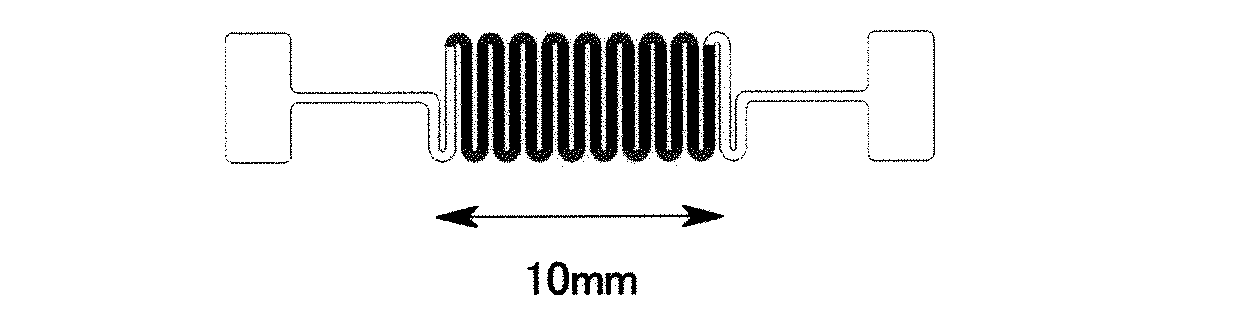
回路パターンは、その一部又は全部が、線状の金属箔ラインが長手方向につづら折り状に折り畳まれた構造を有する。当該構造の回路パターンは、つづら折り状の蛇行回路パターンということができる。 The circuit pattern has a structure in which a part or all of the linear metal foil line is folded in a zigzag shape in the longitudinal direction. The circuit pattern of the structure can be said to be a zigzag meandering circuit pattern.
線(ライン)は幅と長さを有する。本発明において、そのラインの、幅を測定する方向を幅方向、長さを測定する方向を長手方向と呼ぶ(図1参照)。金属箔ラインが、長手方向につづら折り状に折り畳まれた構造の例を図2に示す。つづら折り状の蛇行回路パターンの長手方向は、折り畳む前の金属箔ラインの長手方向と一致する。別の言い方をすれば、つづら折り状の蛇行回路パターンの長手方向は、当該蛇行回路の蛇行を文字通り蛇が曲がりくねって進むと考えた場合に、蛇の進行方向と平行方向であるということもできる。本明細書においては、つづら折り状の蛇行回路パターンの長手方向のことを、第1方向とよぶことがある。 A line has a width and a length. In the present invention, the direction of measuring the width of the line is referred to as the width direction, and the direction of measuring the length is referred to as the longitudinal direction (see FIG. 1). FIG. 2 shows an example of a structure in which the metal foil line is folded in a zigzag shape in the longitudinal direction. The longitudinal direction of the zigzag meandering circuit pattern coincides with the longitudinal direction of the metal leaf line before folding. In other words, the longitudinal direction of the zigzag meandering circuit pattern can be said to be parallel to the traveling direction of the snake, when the meandering of the meandering circuit is considered to be literally winding. In the present specification, the longitudinal direction of the zigzag meandering circuit pattern may be referred to as the first direction.
本明細書では、つづら折り状の蛇行回路パターンの幅は、蛇行したパターンの幅をいう。また、回路パターンの金属箔ラインの幅は、つづら折り状に折り畳む前の金属箔ラインの幅と同じである。また、つづら折り状の蛇行回路パターンの長さは、つづら折り状の蛇行回路パターンの長手方向の長さをいう。つづら折り状の蛇行回路パターンの金属箔ラインの長さとは、つづら折り状に折り畳まれた金属箔ラインの長さをいう。つまり、つづら折り状の蛇行回路パターンの金属箔ラインの幅及び長さは、それぞれ、折り畳む前の金属箔ラインの幅及び長さと同じであり、つづら折り状の蛇行回路パターンの幅及び長さは、折り畳んだ後のパターンの幅及び長手方向の長さ(第1方向の長さ)をいう(図3参照)。本明細書において、回路パターンの金属箔ラインの長さのことを、回路パターンライン長と呼ぶことがある。また、つづら折り状の蛇行回路パターンの長さのことを、第1方向長と呼ぶことがある。第1方向長は、特に制限はされないが、例えば5mm以上であることが好ましく、10mm以上であることがより好ましい。 In the present specification, the width of the zigzag meandering circuit pattern means the width of the meandering pattern. Further, the width of the metal leaf line of the circuit pattern is the same as the width of the metal leaf line before folding in a zigzag shape. The length of the zigzag meandering circuit pattern means the length of the zigzag meandering circuit pattern in the longitudinal direction. The length of the metal leaf line of the zigzag meandering circuit pattern means the length of the metal leaf line folded in a zigzag shape. That is, the width and length of the metal leaf line of the zigzag meandering circuit pattern are the same as the width and length of the metal leaf line before folding, respectively, and the width and length of the zigzag meandering circuit pattern are folded. The width and length of the pattern in the longitudinal direction (length in the first direction) after that (see FIG. 3). In the present specification, the length of the metal leaf line of the circuit pattern may be referred to as the circuit pattern line length. Further, the length of the zigzag meandering circuit pattern may be referred to as the length in the first direction. The length in the first direction is not particularly limited, but is preferably 5 mm or more, and more preferably 10 mm or more, for example.
本明細書における、つづら折り状の蛇行回路パターンは、当該蛇行回路パターンの長手方向と直行方向に略平行な金属箔ライン(「配線部」ということがある)と、配線部どうしを接続する金属箔ライン(「接続部」ということがある)とに分けて考えることもできる。換言すれば、前記蛇行回路パターンは、蛇行回路パターンの長手方向に隣り合う配線が相互に略平行状態を成している配線部と、当該配線部どうしを接続する接続部とからなるということができる。配線部は略直線金属箔ラインからなる。配線部の長さ(図3参照)は、式(1)が満たされる範囲であれば特に制限されず、0mm以上であればよい。例えばほぼ0mmであってもよいし、10000mm程度であってもよい。例えば0mm以上10000mm以下(また例えば、5000mm以下、3000mm以下、1000mm以下、又は500mm以下)であることが好ましい。また、配線部どうしの間隔(図3参照)も式(1)が満たされる範囲であれば特に制限はされず、例えば0.1mm〜5mm程度が例示される。例えば0.1mm以上3mm以下がより好ましく、0.5mm以上2mm以下がさらに好ましい。 In the present specification, the meandering circuit pattern in a zigzag shape is a metal leaf line (sometimes referred to as a "wiring portion") substantially parallel to the longitudinal direction and the perpendicular direction of the meandering circuit pattern, and a metal foil connecting the wiring portions. It can also be thought of as a line (sometimes called a "connection"). In other words, the meandering circuit pattern is composed of a wiring portion in which wirings adjacent to each other in the longitudinal direction of the meandering circuit pattern are substantially parallel to each other and a connection portion connecting the wiring portions. it can. The wiring part consists of a substantially straight metal leaf line. The length of the wiring portion (see FIG. 3) is not particularly limited as long as the equation (1) is satisfied, and may be 0 mm or more. For example, it may be approximately 0 mm or about 10,000 mm. For example, it is preferably 0 mm or more and 10000 mm or less (for example, 5000 mm or less, 3000 mm or less, 1000 mm or less, or 500 mm or less). Further, the distance between the wiring portions (see FIG. 3) is not particularly limited as long as the equation (1) is satisfied, and for example, about 0.1 mm to 5 mm is exemplified. For example, 0.1 mm or more and 3 mm or less is more preferable, and 0.5 mm or more and 2 mm or less is further preferable.
また、回路パターンの金属箔ライン幅も特に制限はされず、例えば0.1mm〜50mm程度が例示される。特に制限はされないが、配線部どうしの間隔は金属箔ライン幅以下であることが好ましい。また、蛇行回路パターンの中において、金属箔ライン幅は変化してもよい(すなわち、一定でなくてもよい)。例えば、蛇行回路パターンのある箇所では0.5mmだが、他のある箇所では1.0mmであってもよい。金属箔ライン幅が変化する場合は、徐々に(滑らかに)ライン幅が変化しても急激にライン幅が変化してもよいが、徐々に(滑らかに)ライン幅が変化することが好ましい。特に制限はされないが、蛇行回路パターンの中で金属箔ラインが変化する場合、最狭部と最広部との幅の比が1:1より大きい〜5程度であることが好ましく、1:2〜3程度であることがより好ましい。 Further, the width of the metal leaf line of the circuit pattern is not particularly limited, and for example, about 0.1 mm to 50 mm is exemplified. Although not particularly limited, it is preferable that the distance between the wiring portions is equal to or less than the width of the metal foil line. Also, in the meandering circuit pattern, the metal leaf line width may vary (ie, may not be constant). For example, it may be 0.5 mm in some places of the meandering circuit pattern, but 1.0 mm in other places. When the metal foil line width changes, the line width may change gradually (smoothly) or abruptly, but it is preferable that the line width changes gradually (smoothly). Although not particularly limited, when the metal leaf line changes in the meandering circuit pattern, the width ratio of the narrowest portion to the widest portion is preferably greater than 1: 1 to about 5, preferably 1: 2. More preferably, it is about ~ 3.
また、接続部は、本発明の効果を損なわず配線部を接続できるなら特に制限はされないが、例えば略U字型、略V字形、略C字型、略I字型(直線)などが挙げられる(図4参照;図4の接続部は上から順に略U字型、略V字形、略C字型、略I字型である。)。 Further, the connecting portion is not particularly limited as long as the wiring portion can be connected without impairing the effect of the present invention, and examples thereof include a substantially U-shape, a substantially V-shape, a substantially C-shape, and a substantially I-shape (straight line). (See FIG. 4; the connection portions in FIG. 4 are substantially U-shaped, substantially V-shaped, substantially C-shaped, and substantially I-shaped in order from the top).
配線部の長さ、接続部の形状、金属箔ラインの幅や長さ等により、様々なつづら折り状の蛇行回路パターンを形成することができる。本発明の効果を損なわない範囲であれば、これら様々なつづら折り状の蛇行回路パターンを用いることできる。特に制限されるわけではないが、いくつかのつづら折り状の蛇行回路パターンを図5a及び図5bに例示する。なお、図5bには、金属箔ライン幅が変化している蛇行回路パターン例を示す。 Various zigzag meandering circuit patterns can be formed depending on the length of the wiring portion, the shape of the connection portion, the width and length of the metal foil line, and the like. These various zigzag meandering circuit patterns can be used as long as the effects of the present invention are not impaired. Although not particularly limited, some zigzag meandering circuit patterns are illustrated in FIGS. 5a and 5b. Note that FIG. 5b shows an example of a meandering circuit pattern in which the width of the metal foil line changes.
また、つづら折り状の蛇行回路パターンにおける折り返し回数(換言すれば接続部の数)は、特に制限されないが、2以上が好ましく、例えば2〜1000程度が例示でき、2〜100程度がより好ましく、5〜50程度がさらに好ましい。 Further, the number of turns (in other words, the number of connecting portions) in the zigzag meandering circuit pattern is not particularly limited, but is preferably 2 or more, for example, about 2 to 1000 can be exemplified, and about 2 to 100 is more preferable. About 50 is more preferable.
また、つづら折り状の蛇行回路パターンの幅は、配線部の長さや接続部の形状等にもよるが、特に制限はされず、例えば、配線部の長さの1.05〜1.7倍程度であることが好ましく、1.1〜1.5倍程度であることがより好ましい。 Further, the width of the zigzag meandering circuit pattern depends on the length of the wiring portion, the shape of the connection portion, etc., but is not particularly limited, and is, for example, about 1.05 to 1.7 times the length of the wiring portion. It is preferably about 1.1 to 1.5 times, and more preferably about 1.1 to 1.5 times.
なお、つづら折り状の蛇行回路パターンを含む複雑な回路パターンであっても、例えば金属箔のエッチングにより、容易に得ることができる。 Even a complicated circuit pattern including a zigzag meandering circuit pattern can be easily obtained by etching a metal foil, for example.
上記の通り、本発明に係る配線基板は、
(式1): E(resin)/4−E(metal)<(B−A)/A×100
も充足する。式(1)に含まれる変数は4つであり、つづら折り状の蛇行回路パターンにおいて、長手方向のA[mm]の範囲における当該蛇行回路パターンの金属箔ライン長がB[mm]であり、また、蛇行回路パターンの長手方向における前記樹脂基板の引張破断伸び率がE(resin)[%]、前記金属箔の引張破断伸び率がE(metal)[%]である。
As described above, the wiring board according to the present invention is
(Equation 1): E (resin) / 4-E (metal) <(BA) / A × 100
Is also satisfied. The number of variables included in the equation (1) is four, and in the meandering circuit pattern of the spiral fold, the metal leaf line length of the meandering circuit pattern in the range of A [mm] in the longitudinal direction is B [mm]. The tensile elongation at break of the resin substrate in the longitudinal direction of the meandering circuit pattern is E (resin) [%], and the elongation at break of the metal foil is E (metal) [%].
ここでの樹脂基板の引張破断伸び率E(resin)[%]はJIS C 2151で測定した値であり、金属箔の引張破断伸び率E(metal)[%]はJIS Z 2241で測定した値である。 Here, the tensile elongation at break E (resin) [%] of the resin substrate is a value measured by JIS C 2151, and the tensile elongation at break E (metal) [%] of the metal foil is a value measured by JIS Z 2241. Is.
本発明に係る配線基板は、上記の構成を有することによって、成型の際に回路が樹脂の伸びに追従できず断線してしまったり、回路が樹脂基板から剥離してしまうことを低減することができる。特に、成型が、前記蛇行回路パターンの長手方向(第1方向)と略直交する曲げ線が形成される方向へ配線基板が曲げられることを含む場合において、特に好適に、樹脂基板からの回路剥離や断線が抑制される。なお、成型において曲げ線が形成される必要はなく、ここでは曲げる方向を説明するために曲げ線という文言を用いただけである。また、「略直交する」とは、特に制限はされないが、第1方向と曲げ線が形成する角度が90°±30°程度が好ましく、90°±20°程度がより好ましく、90°±10°程度がさらに好ましく、90°±5°程度がよりさらに好ましく、約90°±3°程度がなお好ましい。 By having the above configuration, the wiring board according to the present invention can reduce the possibility that the circuit cannot follow the elongation of the resin and is broken or the circuit is peeled off from the resin board during molding. it can. Particularly preferably, when the molding involves bending the wiring board in a direction in which a bending line substantially orthogonal to the longitudinal direction (first direction) of the meandering circuit pattern is formed, the circuit is peeled off from the resin substrate. And disconnection are suppressed. It should be noted that it is not necessary for the bending line to be formed in the molding, and here, the word "bending line" is only used to explain the bending direction. Further, "substantially orthogonal" is not particularly limited, but the angle formed by the bending line from the first direction is preferably about 90 ° ± 30 °, more preferably about 90 ° ± 20 °, and 90 ° ± 10 About ° is even more preferable, about 90 ° ± 5 ° is even more preferable, and about 90 ° ± 3 ° is still more preferable.
より大きな観点からみれば、本発明に係る配線基板において、つづら折り状の蛇行回路パターンは、成型時に第1方向へ伸張可能であるということができ、第1方向へ回路が引き延ばされる力が加わっても(例えば第1方向と略直交する曲げ線が形成される方向へ配線基板が曲げられても)当該回路パターンは剥離や断線を起こしづらいということができる。 From a larger point of view, in the wiring board according to the present invention, it can be said that the meandering circuit pattern in a zigzag shape can be extended in the first direction at the time of molding, and a force for extending the circuit in the first direction is applied. However (for example, even if the wiring board is bent in the direction in which the bending line substantially orthogonal to the first direction is formed), it can be said that the circuit pattern is less likely to cause peeling or disconnection.
各種金属箔からなるつづら折り状の蛇行回路パターン及び直線状回路パターンを備えた配線基板(フィルム)を折り曲げた際、直線状回路パターンでは断線が起こるが、蛇行回路パターンでは断線は起こらないことを示す写真を図8に示す。 It is shown that when a wiring board (film) having a zigzag meandering circuit pattern and a linear circuit pattern made of various metal foils is bent, the linear circuit pattern causes disconnection, but the meandering circuit pattern does not cause disconnection. The photograph is shown in FIG.
従って、本発明に係る配線基板は、前記蛇行回路パターンの長手方向(第1方向)へ回路が引き延ばされる力が加わる成型(例えば、第1方向と略直交する曲げ線が形成される方向へ配線基板が曲げられることを含む成型)用として、特に好ましく用いられる。 Therefore, the wiring board according to the present invention is molded in a direction in which a force for extending the circuit is applied in the longitudinal direction (first direction) of the meandering circuit pattern (for example, in a direction in which a bending line substantially orthogonal to the first direction is formed). It is particularly preferably used for molding) including bending of a wiring board.
本発明は、上記配線基板の成型加工物も好ましく包含する。上記の通り、本発明に係る配線基板は、前記蛇行回路パターンの長手方向(第1方向)へ回路が引き延ばされる力が加わる成型用として、特に好ましく用いられるから、当該力が加えられて成型された成型物が、特に好ましい。また、本発明は、上記配線基板や上記成型物が備えられた構成物も好ましく包含する。 The present invention preferably also includes a molded product of the wiring board. As described above, the wiring board according to the present invention is particularly preferably used for molding in which a force for extending the circuit is applied in the longitudinal direction (first direction) of the meandering circuit pattern. The molded product is particularly preferable. The present invention also preferably includes a component provided with the wiring board and the molded product.
特に制限はされないが、例えば、本発明に係る配線基板が自動車のダッシュボードの形に成型された場合、例えば当該成型済み配線基板が成型物に該当し、例えば当該成型物が備えられた自動車のダッシュボード(さらには当該自動車のダッシュボードが備えられた自動車)が構成物に該当する。 Although not particularly limited, for example, when the wiring board according to the present invention is molded in the shape of a dashboard of an automobile, for example, the molded wiring board corresponds to a molded product, for example, an automobile provided with the molded product. The dashboard (and the vehicle equipped with the dashboard of the vehicle) corresponds to the component.
なお、本明細書において「含む」とは、「本質的にからなる」と、「からなる」をも包含する(The term "comprising" includes "consisting essentially of” and "consisting of.")。 In addition, in this specification, "including" also includes "consisting essentially" and "consisting of" (The term "comprising" includes "consisting essentially of" and "consisting of.").
以下、本発明を具体的に説明するが、本発明は下記の例に限定されるものではない。
(実施例1)
厚さ80μmのアルミニウム箔(東洋アルミ二ウム株式会社製、1N30、硬質材:引張破断伸び率は6%、0.2%耐力は150N/mm2)の片面に、接着性樹脂(DIC株式会社製ウレタン系接着剤:LX500を100部と、硬化剤であるKW75を10部混合した)を塗工・乾燥させた後に、厚み60μmのポリプロピレンフィルム(フタムラ化学株式会社製FRTK−G)と貼り合わせた。なお、当該アルミニウム箔の引張破断伸び率及び0.2%耐力はJIS Z 2241により測定した。
Hereinafter, the present invention will be specifically described, but the present invention is not limited to the following examples.
(Example 1)
Adhesive resin (DIC Co., Ltd.) on one side of 80 μm thick aluminum foil (manufactured by Toyo Aluminum Co., Ltd., 1N30, hard material: tensile elongation at break 6%, 0.2% proof stress 150 N / mm 2) Urethane adhesive: 100 parts of LX500 and 10 parts of KW75, which is a curing agent, are mixed), coated and dried, and then bonded to a polypropylene film (FRTK-G manufactured by Futamura Chemical Co., Ltd.) with a thickness of 60 μm. It was. The tensile elongation at break and 0.2% proof stress of the aluminum foil were measured by JIS Z 2241.
次に、フォトリソグラフィー法によりアルミニウム箔をつづら折り状の蛇行パターンの回路へ形成した。当該回路パターンの概要を図6に示す。当該回路パターンにおいて、金属箔ライン幅は1mmであり、回路の配線部同士の間隔は約0.3mmであり、接続部は略U字型であり、接続部外縁は半円状である。 Next, the aluminum foil was formed into a zigzag meandering pattern circuit by a photolithography method. The outline of the circuit pattern is shown in FIG. In the circuit pattern, the metal leaf line width is 1 mm, the distance between the wiring portions of the circuit is about 0.3 mm, the connection portion is substantially U-shaped, and the outer edge of the connection portion is semicircular.
つづら折り状の蛇行回路パターンの長手方向(第1方向)の長さを10mmとし、この範囲内の回路の全長(回路パターンライン長)が30mmとなるようにした。また使用したポリプロピレンフィルム単体の、第1方向の引張破断伸び率は500%であった。なお、当該ポリプロピレンフィルムの第1方向の引張破断伸び率はJIS C 2151により測定した。 The length of the zigzag meandering circuit pattern in the longitudinal direction (first direction) was set to 10 mm, and the total length of the circuit within this range (circuit pattern line length) was set to 30 mm. The tensile elongation at break in the first direction of the polypropylene film used alone was 500%. The tensile elongation at break in the first direction of the polypropylene film was measured by JIS C 2151.
こうして得られた試験体に対して成型加工を行った。成型加工は、図7に示す様に、得られた試験体を回路パターン面と型が接するように固定し、先端がR(半径)2.5mmの半球上になった金属性の冶具を、50mm/分の速度で押し当てることで行った。この時、試験体に対する押し当てる冶具の位置は図6で示した回路における、10mmの範囲の中心辺りとした。また冶具を押し込む深さは、予め試験体が破断する深さの確認を行い、その深さの50%とした。 The test body thus obtained was molded. In the molding process, as shown in FIG. 7, the obtained test piece was fixed so that the circuit pattern surface and the mold were in contact with each other, and a metallic jig having a tip on a hemisphere with an R (radius) of 2.5 mm was used. This was done by pressing at a speed of 50 mm / min. At this time, the position of the jig to be pressed against the test piece was set to be around the center of the range of 10 mm in the circuit shown in FIG. Further, the depth at which the jig was pushed was set to 50% of the depth at which the depth at which the test piece was broken was confirmed in advance.
(実施例2〜8および比較例1〜6)
表1に記載した金属箔、樹脂層、回路パターンを採用した以外は、実施例1と同様にして、試験体を作製した。なお、各例によって、回路パターンライン長が異なるが、これは配線部の長さを変更することで調節したものである。
(Examples 2 to 8 and Comparative Examples 1 to 6)
A test body was prepared in the same manner as in Example 1 except that the metal foil, resin layer, and circuit pattern shown in Table 1 were adopted. The circuit pattern line length differs depending on each example, but this is adjusted by changing the length of the wiring portion.
また、各例に用いた金属箔の引張破断伸び率(E(metal))及び0.2%耐力はJIS Z 2241により、各例に用いた樹脂層(樹脂フィルム又はシート)の引張破断伸び率(E(resin))はJIS C 2151により、それぞれ測定した。 In addition, the tensile elongation at break (E (metal)) and 0.2% proof stress of the metal foil used in each example are based on JIS Z 2241, and the tensile elongation at break of the resin layer (resin film or sheet) used in each example. (E (resin)) was measured by JIS C 2151, respectively.
<評価項目及び評価基準>
上記のようにして得られた各実施例及び比較例の試験体について、以下の(A)及び(B)の観点から評価を行った。結果を表1に併せて示す。
<Evaluation items and evaluation criteria>
The test bodies of each Example and Comparative Example obtained as described above were evaluated from the viewpoints of (A) and (B) below. The results are also shown in Table 1.
(A)成型後の回路パターンの断線
各実施例、比較例で得られた試験体について目視観察および電気抵抗値測定を行い、回路パターンの断線が生じているかを確認した。評価結果は次のとおりに表示する。
(A) Disconnection of circuit pattern after molding The test pieces obtained in each Example and Comparative Example were visually observed and the electric resistance value was measured, and it was confirmed whether or not the circuit pattern was disconnected. The evaluation results are displayed as follows.
○:回路パターンの断線無し。
×:回路パターンの断線有り。
◯: No disconnection of the circuit pattern.
X: There is a disconnection in the circuit pattern.
(B)成型後の樹脂層の歪み
各実施例、比較例で得られた試験体について目視観察を行い、回路パターンが存在する近辺での樹脂層の歪みが生じているかを確認した。評価結果は次のとおりに表示する。
(B) Distortion of the resin layer after molding The test pieces obtained in each Example and Comparative Example were visually observed to confirm whether the resin layer was distorted in the vicinity of the circuit pattern. The evaluation results are displayed as follows.
○:樹脂層の歪み無し。
×:樹脂層の歪み有り。
◯: No distortion of the resin layer.
X: The resin layer is distorted.
以上の結果が示す様に、
式(1): E(resin)/4−E(metal)<(B−A)/A×100
式(2): (F×T)≦22000
をいずれも満たす配線基板は、大電流を流すことも可能でありながら、成型の際に回路の断線や剥離を抑制することもできることがわかった。
As the above results show
Equation (1): E (resin) / 4-E (metal) <(BA) / A × 100
Equation (2): (F × T) ≦ 22000
It was found that a wiring board that satisfies all of the above conditions can pass a large current and can suppress disconnection and peeling of a circuit during molding.
Claims (7)
前記回路パターンの一部又は全部が、線状の金属箔ラインが長手方向につづら折り状に折り畳まれた構造を有する、つづら折り状の蛇行回路パターンであり、
前記金属箔はアルミニウム箔であり、
前記蛇行回路パターンの長手方向のA[mm]の範囲における当該蛇行回路パターンの金属箔ライン長をB[mm]とし、
当該蛇行回路パターンの長手方向における前記樹脂基板の引張破断伸び率をJIS C 2151で測定した値をE(resin)[%]、前記金属箔の引張破断伸び率をJIS Z 2241で測定した値をE(metal)[%]とし、
当該金属箔の25℃での0.2%耐力をJIS Z 2241で測定した値をF[N/mm2]、厚みをT[μm]としたとき、
以下の式(1)と式(2)を満たす、配線基板。
式(1): E(resin)/4−E(metal)<(B−A)/A×100
式(2): (F×T)≦22000 A wiring board having a circuit pattern made of metal foil on at least one side of a resin board.
A part or all of the circuit pattern is a zigzag meandering circuit pattern having a structure in which linear metal leaf lines are folded in a zigzag shape in the longitudinal direction.
The metal foil is an aluminum foil.
The metal leaf line length of the meandering circuit pattern in the range of A [mm] in the longitudinal direction of the meandering circuit pattern is defined as B [mm].
The value measured by JIS C 2151 for the tensile elongation at break of the resin substrate in the longitudinal direction of the meandering circuit pattern is E (resin) [%], and the tensile elongation at break of the metal foil is measured by JIS Z 2241. E (metal) [%]
When the 0.2% proof stress of the metal foil at 25 ° C. was measured by JIS Z 2241 as F [N / mm 2 ] and the thickness was T [μm].
A wiring board that satisfies the following equations (1) and (2).
Equation (1): E (resin) / 4-E (metal) <(BA) / A × 100
Equation (2): (F × T) ≦ 22000
Priority Applications (2)
| Application Number | Priority Date | Filing Date | Title |
|---|---|---|---|
| JP2016249490A JP6851813B2 (en) | 2016-12-22 | 2016-12-22 | Wiring board |
| CN201711376537.8A CN108235567B (en) | 2016-12-22 | 2017-12-19 | Wiring board |
Applications Claiming Priority (1)
| Application Number | Priority Date | Filing Date | Title |
|---|---|---|---|
| JP2016249490A JP6851813B2 (en) | 2016-12-22 | 2016-12-22 | Wiring board |
Publications (2)
| Publication Number | Publication Date |
|---|---|
| JP2018107193A JP2018107193A (en) | 2018-07-05 |
| JP6851813B2 true JP6851813B2 (en) | 2021-03-31 |
Family
ID=62652486
Family Applications (1)
| Application Number | Title | Priority Date | Filing Date |
|---|---|---|---|
| JP2016249490A Active JP6851813B2 (en) | 2016-12-22 | 2016-12-22 | Wiring board |
Country Status (2)
| Country | Link |
|---|---|
| JP (1) | JP6851813B2 (en) |
| CN (1) | CN108235567B (en) |
Families Citing this family (2)
| Publication number | Priority date | Publication date | Assignee | Title |
|---|---|---|---|---|
| CN109686253B (en) * | 2019-01-08 | 2021-04-23 | 云谷(固安)科技有限公司 | Wiring structure and stretchable display device |
| JP7267468B2 (en) * | 2020-02-06 | 2023-05-01 | 三菱電機株式会社 | Semiconductor module and power converter |
Family Cites Families (16)
| Publication number | Priority date | Publication date | Assignee | Title |
|---|---|---|---|---|
| JP2956451B2 (en) * | 1993-10-25 | 1999-10-04 | 住友電装株式会社 | Method of fixing flat circuit body and flat circuit body used therefor |
| JP2000261109A (en) * | 1999-03-11 | 2000-09-22 | Sharp Corp | Wiring board |
| US7002430B2 (en) * | 2003-05-30 | 2006-02-21 | Intel Corporation | Compact non-linear geometry electromagnetic coupler for use with digital transmission systems |
| JP2005217156A (en) * | 2004-01-29 | 2005-08-11 | Sumitomo Electric Ind Ltd | Manufacturing method of three-dimensional injection molded circuit components |
| JP2006156913A (en) * | 2004-12-01 | 2006-06-15 | Ricoh Co Ltd | Printed wiring board |
| JP2007005640A (en) * | 2005-06-24 | 2007-01-11 | Three M Innovative Properties Co | Circuit board interconnection method |
| JP4699149B2 (en) * | 2005-09-15 | 2011-06-08 | ジャパンゴアテックス株式会社 | Circuit board, thin film solar cell, and manufacturing method thereof |
| JP2007194341A (en) * | 2006-01-18 | 2007-08-02 | Kyocera Chemical Corp | Flexible printed wiring board and manufacturing method thereof |
| DE102008031573B4 (en) * | 2008-07-07 | 2012-06-28 | Carl Freudenberg Kg | Stretchable fleece with ladder structures |
| JP5717961B2 (en) * | 2009-12-24 | 2015-05-13 | 日本メクトロン株式会社 | Method for manufacturing flexible circuit board |
| CN102629337A (en) * | 2012-04-12 | 2012-08-08 | 上海祯显电子科技有限公司 | Micro intelligent label |
| US9226402B2 (en) * | 2012-06-11 | 2015-12-29 | Mc10, Inc. | Strain isolation structures for stretchable electronics |
| JP2013139587A (en) * | 2013-04-22 | 2013-07-18 | Mitsubishi Chemicals Corp | Resin composition, and molding and film comprising the same |
| KR102093159B1 (en) * | 2014-05-23 | 2020-03-25 | 삼성전기주식회사 | Printed circuit board and printed circuit board for camera module |
| JP6362444B2 (en) * | 2014-06-16 | 2018-07-25 | 日本メクトロン株式会社 | Flexible printed circuit board and method for manufacturing flexible printed circuit board |
| US20160105950A1 (en) * | 2014-10-10 | 2016-04-14 | Apple Inc. | Electronic Device Having Structured Flexible Substrates With Bends |
-
2016
- 2016-12-22 JP JP2016249490A patent/JP6851813B2/en active Active
-
2017
- 2017-12-19 CN CN201711376537.8A patent/CN108235567B/en not_active Expired - Fee Related
Also Published As
| Publication number | Publication date |
|---|---|
| CN108235567B (en) | 2022-02-11 |
| JP2018107193A (en) | 2018-07-05 |
| CN108235567A (en) | 2018-06-29 |
Similar Documents
| Publication | Publication Date | Title |
|---|---|---|
| CN106133663B (en) | touch sensor | |
| EP2695733B1 (en) | Copper foil composite, copper foil used for the same, formed product and method of producing the same | |
| TWI646207B (en) | Copper foil for flexible printed circuit board, copper-clad laminate using the same, flexible printed circuit board, and electronic device | |
| JP6294376B2 (en) | Copper foil for flexible printed circuit board, copper-clad laminate using the same, flexible printed circuit board, and electronic device | |
| JP6851813B2 (en) | Wiring board | |
| JP2017005214A5 (en) | ||
| US20090038828A1 (en) | Flexible printed circuit board substrate and flexible printed circuit board fabricated using the same | |
| CN107046763B (en) | Copper foil for flexible printed circuit board, copper clad laminate using same | |
| CN112210689B (en) | Copper foil for flexible printed circuit boards | |
| JP6515808B2 (en) | Flat cable | |
| JP2006339295A (en) | Flexible circuit board | |
| JP2018174201A (en) | WIRING BOARD, STRUCTURE PROVIDED WITH THE WIRING BOARD, AND WIRING BOARD INSTALLATION METHOD | |
| WO2017056240A1 (en) | Pressure-sensitive sensor | |
| CN107046768B (en) | Copper foil for flexible printed circuit boards, copper clad laminates using the same, flexible printed circuit boards, and electronic devices | |
| CN111757599B (en) | Copper foil for flexible printed board | |
| JP4398311B2 (en) | Flexible printed circuit board | |
| JP2008279610A (en) | Flexible laminate and method for producing flexible laminate | |
| JP6884619B2 (en) | A wiring board, a structure including the wiring board, and a method of attaching the wiring board | |
| CN109385556A (en) | Copper foil for flexible printed circuit board, copper-clad laminate using the copper foil, flexible printed circuit board, and electronic device | |
| CN102574364B (en) | Method of manufacturing double-sided copper-clad laminate, and pair of copper or copper alloy foil sheets used thereupon | |
| WO2009091005A1 (en) | Composite material for electrical/electronic component, electrical/electronic component, and method for producing composite material for electrical/electronic component | |
| JP7628422B2 (en) | Manufacturing method of magnetic member and magnetic member | |
| JP5830571B2 (en) | Flexible cable | |
| JP4612408B2 (en) | Circuit structure | |
| TWI774850B (en) | Subsequent tape and subsequent tape winding reels |
Legal Events
| Date | Code | Title | Description |
|---|---|---|---|
| A621 | Written request for application examination |
Free format text: JAPANESE INTERMEDIATE CODE: A621 Effective date: 20190902 |
|
| A977 | Report on retrieval |
Free format text: JAPANESE INTERMEDIATE CODE: A971007 Effective date: 20200529 |
|
| A131 | Notification of reasons for refusal |
Free format text: JAPANESE INTERMEDIATE CODE: A131 Effective date: 20200623 |
|
| A521 | Request for written amendment filed |
Free format text: JAPANESE INTERMEDIATE CODE: A523 Effective date: 20200812 |
|
| A02 | Decision of refusal |
Free format text: JAPANESE INTERMEDIATE CODE: A02 Effective date: 20210105 |
|
| A521 | Request for written amendment filed |
Free format text: JAPANESE INTERMEDIATE CODE: A523 Effective date: 20210120 |
|
| C60 | Trial request (containing other claim documents, opposition documents) |
Free format text: JAPANESE INTERMEDIATE CODE: C60 Effective date: 20210120 |
|
| A911 | Transfer to examiner for re-examination before appeal (zenchi) |
Free format text: JAPANESE INTERMEDIATE CODE: A911 Effective date: 20210129 |
|
| C21 | Notice of transfer of a case for reconsideration by examiners before appeal proceedings |
Free format text: JAPANESE INTERMEDIATE CODE: C21 Effective date: 20210202 |
|
| TRDD | Decision of grant or rejection written | ||
| A01 | Written decision to grant a patent or to grant a registration (utility model) |
Free format text: JAPANESE INTERMEDIATE CODE: A01 Effective date: 20210302 |
|
| A61 | First payment of annual fees (during grant procedure) |
Free format text: JAPANESE INTERMEDIATE CODE: A61 Effective date: 20210310 |
|
| R150 | Certificate of patent or registration of utility model |
Ref document number: 6851813 Country of ref document: JP Free format text: JAPANESE INTERMEDIATE CODE: R150 |
|
| R250 | Receipt of annual fees |
Free format text: JAPANESE INTERMEDIATE CODE: R250 |
|
| R250 | Receipt of annual fees |
Free format text: JAPANESE INTERMEDIATE CODE: R250 |