JP6821982B2 - Manufacturing method of thin film transistor, display device and thin film transistor - Google Patents
Manufacturing method of thin film transistor, display device and thin film transistor Download PDFInfo
- Publication number
- JP6821982B2 JP6821982B2 JP2016138874A JP2016138874A JP6821982B2 JP 6821982 B2 JP6821982 B2 JP 6821982B2 JP 2016138874 A JP2016138874 A JP 2016138874A JP 2016138874 A JP2016138874 A JP 2016138874A JP 6821982 B2 JP6821982 B2 JP 6821982B2
- Authority
- JP
- Japan
- Prior art keywords
- insulating film
- gate insulating
- region
- film
- oxide semiconductor
- Prior art date
- Legal status (The legal status is an assumption and is not a legal conclusion. Google has not performed a legal analysis and makes no representation as to the accuracy of the status listed.)
- Active
Links
Images


Classifications
-
- H—ELECTRICITY
- H10—SEMICONDUCTOR DEVICES; ELECTRIC SOLID-STATE DEVICES NOT OTHERWISE PROVIDED FOR
- H10D—INORGANIC ELECTRIC SEMICONDUCTOR DEVICES
- H10D30/00—Field-effect transistors [FET]
- H10D30/60—Insulated-gate field-effect transistors [IGFET]
- H10D30/67—Thin-film transistors [TFT]
- H10D30/674—Thin-film transistors [TFT] characterised by the active materials
- H10D30/6755—Oxide semiconductors, e.g. zinc oxide, copper aluminium oxide or cadmium stannate
-
- H—ELECTRICITY
- H10—SEMICONDUCTOR DEVICES; ELECTRIC SOLID-STATE DEVICES NOT OTHERWISE PROVIDED FOR
- H10D—INORGANIC ELECTRIC SEMICONDUCTOR DEVICES
- H10D30/00—Field-effect transistors [FET]
- H10D30/60—Insulated-gate field-effect transistors [IGFET]
- H10D30/67—Thin-film transistors [TFT]
- H10D30/6729—Thin-film transistors [TFT] characterised by the electrodes
- H10D30/673—Thin-film transistors [TFT] characterised by the electrodes characterised by the shapes, relative sizes or dispositions of the gate electrodes
-
- H—ELECTRICITY
- H10—SEMICONDUCTOR DEVICES; ELECTRIC SOLID-STATE DEVICES NOT OTHERWISE PROVIDED FOR
- H10D—INORGANIC ELECTRIC SEMICONDUCTOR DEVICES
- H10D30/00—Field-effect transistors [FET]
- H10D30/60—Insulated-gate field-effect transistors [IGFET]
- H10D30/67—Thin-film transistors [TFT]
- H10D30/6729—Thin-film transistors [TFT] characterised by the electrodes
- H10D30/6737—Thin-film transistors [TFT] characterised by the electrodes characterised by the electrode materials
- H10D30/6739—Conductor-insulator-semiconductor electrodes
-
- H—ELECTRICITY
- H10—SEMICONDUCTOR DEVICES; ELECTRIC SOLID-STATE DEVICES NOT OTHERWISE PROVIDED FOR
- H10D—INORGANIC ELECTRIC SEMICONDUCTOR DEVICES
- H10D64/00—Electrodes of devices having potential barriers
- H10D64/01—Manufacture or treatment
-
- H—ELECTRICITY
- H10—SEMICONDUCTOR DEVICES; ELECTRIC SOLID-STATE DEVICES NOT OTHERWISE PROVIDED FOR
- H10D—INORGANIC ELECTRIC SEMICONDUCTOR DEVICES
- H10D64/00—Electrodes of devices having potential barriers
- H10D64/20—Electrodes characterised by their shapes, relative sizes or dispositions
- H10D64/27—Electrodes not carrying the current to be rectified, amplified, oscillated or switched, e.g. gates
- H10D64/311—Gate electrodes for field-effect devices
- H10D64/411—Gate electrodes for field-effect devices for FETs
- H10D64/511—Gate electrodes for field-effect devices for FETs for IGFETs
- H10D64/514—Gate electrodes for field-effect devices for FETs for IGFETs characterised by the insulating layers
-
- H—ELECTRICITY
- H10—SEMICONDUCTOR DEVICES; ELECTRIC SOLID-STATE DEVICES NOT OTHERWISE PROVIDED FOR
- H10D—INORGANIC ELECTRIC SEMICONDUCTOR DEVICES
- H10D64/00—Electrodes of devices having potential barriers
- H10D64/60—Electrodes characterised by their materials
- H10D64/66—Electrodes having a conductor capacitively coupled to a semiconductor by an insulator, e.g. MIS electrodes
- H10D64/68—Electrodes having a conductor capacitively coupled to a semiconductor by an insulator, e.g. MIS electrodes characterised by the insulator, e.g. by the gate insulator
- H10D64/681—Electrodes having a conductor capacitively coupled to a semiconductor by an insulator, e.g. MIS electrodes characterised by the insulator, e.g. by the gate insulator having a compositional variation, e.g. multilayered
-
- H—ELECTRICITY
- H10—SEMICONDUCTOR DEVICES; ELECTRIC SOLID-STATE DEVICES NOT OTHERWISE PROVIDED FOR
- H10D—INORGANIC ELECTRIC SEMICONDUCTOR DEVICES
- H10D99/00—Subject matter not provided for in other groups of this subclass
Landscapes
- Thin Film Transistor (AREA)
- Electroluminescent Light Sources (AREA)
Description
本発明は、薄膜トランジスタ、表示装置及び薄膜トランジスタの製造方法に関する。 The present invention relates to a thin film transistor, a display device, and a method for manufacturing a thin film transistor.
インジウム−ガリウム−亜鉛の酸化物(以下、InGaZnO)を代表とする酸化物半導体を用いた酸化物半導体薄膜トランジスタは、シリコン系半導体薄膜トランジスタに比べて、大面積上に良好な電気特性が実現できる。以下の説明では薄膜トランジスタをTFT(Thin Film Transistor)と記載する場合がある。 An oxide semiconductor thin film transistor using an oxide semiconductor typified by an oxide of indium-gallium-zinc (hereinafter, InGaZnO) can realize good electrical characteristics on a large area as compared with a silicon-based semiconductor thin film transistor. In the following description, the thin film transistor may be referred to as a TFT (Thin Film Transistor).
酸化物半導体TFTの、液晶ディスプレイ及び有機EL(Electro-Luminescence)ディスプレイへの適用が一部で始まっている。以下の説明では、液晶ディスプレイをLCD(Liquid Crystal Display)と記載する。また有機ELディスプレイをOLED(Organic Electro-Luminescence Display)と記載する。 The application of oxide semiconductor TFTs to liquid crystal displays and organic EL (Electro-Luminescence) displays has begun in part. In the following description, the liquid crystal display will be referred to as LCD (Liquid Crystal Display). Further, the organic EL display is described as OLED (Organic Electro-Luminescence Display).
酸化物半導体TFTの現在の主流はボトムゲート型TFTである。大型のLCDまたはOLEDを高速駆動する場合には、セルフアライン・トップゲート型TFTが有利である。セルフアライン・トップゲート型TFTは、ゲート電極とソース電極またはドレイン電極とが重なる領域及びゲート電極とソース領域またはドレイン領域とが重なる領域で発生する寄生容量が少ない。 The current mainstream of oxide semiconductor TFTs is bottom gate type TFTs. When driving a large LCD or OLED at high speed, a self-aligned top gate type TFT is advantageous. In the self-aligned top gate type TFT, the parasitic capacitance generated in the region where the gate electrode and the source electrode or the drain electrode overlap and the region where the gate electrode and the source region or the drain region overlap is small.
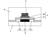
図27は、特許文献1に開示されているセルフアライン・トップゲート型TFTの概略断面図である。セルフアライン・トップゲート型TFTは、基板1、酸化物半導体層2、ゲート絶縁膜3、ゲート電極4、ソース側コンタクトホール62、ドレイン側コンタクトホール63、ソース電極72、ドレイン電極73及び層間絶縁膜5を有する。酸化物半導体層2はチャネル領域21、ソース領域22及びドレイン領域23を有する。
FIG. 27 is a schematic cross-sectional view of the self-aligned top gate type TFT disclosed in
特許文献1では、水素がドナーとして働くことにより抵抗が変化する酸化物半導体の性質を利用している。すなわち、ゲート絶縁膜3に水素の少ない窒化シリコン膜を用いることでチャネル領域21中の水素を少なくする。これにより、チャネル領域21の高抵抗を維持する。層間絶縁膜5には水素の多い窒化シリコン膜を用いることで、ソース領域22及びドレイン領域23の中へ水素を多く拡散させる。これにより、ソース領域22及びドレイン領域23を低抵抗化している。
特許文献2に、ゲート電極4に水素の拡散を抑制する機能を持たせることにより、層間絶縁膜5を成膜する際のチャネル領域21中への水素の拡散を抑制するトップゲート型TFTが開示されている。
特許文献1及び特許文献2では、ゲート電極4とゲート絶縁膜3とを同一のパターンで形成し、このパターンをマスクに層間絶縁膜5から水素を拡散させ、ソース領域22及びドレイン領域23を形成する。そのため、層間絶縁膜5の成膜時には、ゲート電極4の端部の直下にチャネル領域21とソース領域22またはドレイン領域23との境界が存在している。そこで、寄生容量を少なくするには、ソース領域22及びドレイン領域23からチャネル領域21へ向かう水素の拡散をできるだけ抑える必要がある。
In
非特許文献1に、水素の拡散係数とその活性化エネルギーを求める方法が開示されている。ソース電極72及びドレイン電極73から酸化物半導体であるInGaZnO層中に水素が拡散することにより、ソース領域22及びドレイン領域23が拡大するというモデルに基づいて、式(1)により水素の拡散係数を、式(2)により活性化エネルギーをそれぞれ求める。
Non-Patent

前述のように、寄生容量を少なくするには、水素の横方向への拡散をできるだけ抑えることが望ましい。そのために、層間絶縁膜5の成膜及びその後のアニールを低温で行う。その結果、TFTの信頼性を確保することは難しくなる。なぜなら、一般的に成膜及び成膜後のアニールを低温で行った絶縁膜の電気特性及び膜質は制約を受け、劣化したものになりやすいためである。
As mentioned above, in order to reduce the parasitic capacitance, it is desirable to suppress the lateral diffusion of hydrogen as much as possible. Therefore, the
このような電気特性の劣化した絶縁膜を層間絶縁膜5に用いる場合には、ゲート電極4のドレイン端でホットキャリア注入が起こりやすい。また、膜質が劣化して、緻密で無い絶縁膜は、水分を含みやすい。水分を含んだ絶縁膜は、分極し易く、アルカリ金属汚染にも弱い。その結果、TFT特性のシフト及びS値劣化が発生しやすくなる。ここで、S値とはドレイン電圧が一定である場合にドレイン電流を1ケタ変化させるサブスレッシュホールド領域でのゲート電圧値である。
When such an insulating film having deteriorated electrical characteristics is used for the
TFTの信頼性を良好にするために層間絶縁膜5の成膜及びアニールを高温で行う場合には、ソース領域22及びドレイン領域23中の水素がチャネル領域21へ横方向に過剰に拡散する。その結果ゲート電極4とソース領域22またはドレイン領域23とがの重なる面積が増え、寄生容量が増加する。
When the
深刻な状況である場合には、ゲート電極4及びゲート絶縁膜3上の層間絶縁膜5から、ゲート電極4及びゲート絶縁膜3を通過して、チャネル領域21中に水素が拡散する。これによりチャネル領域21中のキャリアが増加して、抵抗値が低下する。その結果、チャネル領域21とソース領域22またはドレイン領域23との間で抵抗値の差が少なくなり、TFTの性能が不十分になる。
In a serious situation, hydrogen diffuses from the
本願は、一つの側面では、低い寄生容量と高い信頼性とを両立した、酸化物半導体TFTを提供することを目的とする。 One aspect of the present application is to provide an oxide semiconductor TFT that has both low parasitic capacitance and high reliability.
一つの態様では、本発明のTFTは、絶縁性の基板と、前記基板上に設けられており、チャネル領域と該チャネル領域よりも抵抗の低いソース領域及びドレイン領域とを含む酸化物半導体層と、前記酸化物半導体層の上に設けられたゲート絶縁膜と、前記ゲート絶縁膜の上に設けられたゲート電極と、前記ゲート電極と前記ゲート絶縁膜と前記酸化物半導体層との上に設けられた膜中に水素を含有する層間絶縁膜と、前記層間絶縁膜に設けられたコンタクトホールを介して前記ソース領域と導通するソース電極と、前記層間絶縁膜に設けられたコンタクトホールを介して前記ドレイン領域と導通するドレイン電極とを有するTFTにおいて、前記ゲート絶縁膜は、一層又は二層からなり、少なくとも前記ゲート絶縁膜のいずれかの層は、前記ソース電極及び前記ドレイン電極と離れた位置にある、パターン化ゲート絶縁膜であり、前記パターン化ゲート絶縁膜の下面のチャネル長方向の長さは、前記ゲート電極の下面のチャネル長方向の長さよりも大きく、前記パターン化ゲート絶縁膜の上面のチャネル長方向の端部は、前記ゲート電極の下面のチャネル長方向の端部と離れており、前記パターン化ゲート絶縁膜の下面のチャネル長方向の長さは、前記チャネル領域のチャネル長方向の長さよりも大きく、前記ソース領域側の前記ゲート電極の端から前記ソース領域側の前記ゲート絶縁膜のうち最も小さい形状を有する最小ゲート絶縁膜の端までの距離が、前記ドレイン領域側の前記ゲート電極の端から前記ドレイン領域側の前記最小ゲート絶縁膜の端までの距離と等しく、前記チャネル領域と前記ソース領域との境界及び前記チャネル領域と前記ドレイン領域との境界は、前記ゲート電極の下にあり、前記ソース領域及び前記ドレイン領域の水素濃度は前記チャネル領域の水素濃度よりも高い。 In one embodiment, the TFT of the present invention comprises an insulating substrate and an oxide semiconductor layer provided on the substrate and including a channel region and a source region and a drain region having lower resistance than the channel region. , The gate insulating film provided on the oxide semiconductor layer, the gate electrode provided on the gate insulating film, the gate electrode, the gate insulating film, and the oxide semiconductor layer. An interlayer insulating film containing hydrogen in the interlayer insulating film, a source electrode that conducts with the source region through a contact hole provided in the interlayer insulating film, and a contact hole provided in the interlayer insulating film. In a TFT having a drain electrode conducting with the drain region, the gate insulating film is composed of one or two layers, and at least one layer of the gate insulating film is located at a position away from the source electrode and the drain electrode. The patterned gate insulating film is located in the above, and the length of the lower surface of the patterned gate insulating film in the channel length direction is larger than the length of the lower surface of the gate electrode in the channel length direction . The end of the upper surface in the channel length direction is separated from the end of the lower surface of the gate electrode in the channel length direction, and the length of the lower surface of the patterned gate insulating film in the channel length direction is the channel length of the channel region. The distance from the end of the gate electrode on the source region side to the end of the smallest gate insulating film having the smallest shape among the gate insulating films on the source region side, which is larger than the length in the direction, is on the drain region side. The distance from the end of the gate electrode to the end of the minimum gate insulating film on the drain region side is equal, and the boundary between the channel region and the source region and the boundary between the channel region and the drain region are equal to the gate electrode. The hydrogen concentration in the source region and the drain region is higher than the hydrogen concentration in the channel region.
一つの側面では、低い寄生容量と高い信頼性とを両立した、酸化物半導体TFTを提供することができる。 On one aspect, it is possible to provide an oxide semiconductor TFT that has both low parasitic capacitance and high reliability.
[実施の形態1]
まず、酸化物半導体の特性について説明する。表1は、酸化物半導体の抵抗及び水素濃度を示す。
[Embodiment 1]
First, the characteristics of the oxide semiconductor will be described. Table 1 shows the resistance and hydrogen concentration of the oxide semiconductor.
成膜前の列は、InGaZnO層の抵抗値及び水素濃度を示す。SiO2の列は、InGaZnO層の上に酸化シリコン膜を100ナノメートルの厚さで成膜した場合のInGaZnO層の抵抗及び水素濃度を示す。Al2O2の列は、InGaZnO層の上に酸化アルミニウム膜を50ナノメートルの厚さで成膜した場合のInGaZnO層の抵抗及び水素濃度を示す。SiO2/Al2O2の列はInGaZnO層の上に酸化アルミニウム膜を50ナノメートルの厚さで成膜し、その上に酸化シリコン膜を100ナノメートル積層した場合の、InGaZnO層の抵抗と水素濃度を示す。 The row before film formation shows the resistance value and hydrogen concentration of the InGaZnO layer. The rows of SiO 2 show the resistance and hydrogen concentration of the InGaZnO layer when a silicon oxide film is formed on the InGaZnO layer to a thickness of 100 nanometers. The rows of Al 2 O 2 show the resistance and hydrogen concentration of the InGaZnO layer when an aluminum oxide film is formed on the InGaZnO layer to a thickness of 50 nanometers. The row of SiO 2 / Al 2 O 2 is the resistance of the InGaZnO layer when an aluminum oxide film is formed on the InGaZnO layer to a thickness of 50 nanometers and a silicon oxide film is laminated on the InGaZnO layer by 100 nanometers. Indicates the hydrogen concentration.
酸化シリコン膜は、プラズマ化学気相堆積法を使用して成膜する。以後の説明ではプラズマ化学気相堆積法をPECVD(Plasma Enhanced Chemical Vapor Deposition)と記載する。酸化シリコン膜は、300℃のチャンバ内にて、オルトケイ酸テトラエチルと酸素ガスとを放電させて成膜する。以後の説明では、オルトケイ酸テトラエチルをTEOS(Tetraethylorthosilicate)と記載する。 The silicon oxide film is formed using a plasma chemical vapor deposition method. In the following description, the plasma chemical vapor deposition method will be referred to as PECVD (Plasma Enhanced Chemical Vapor Deposition). The silicon oxide film is formed by discharging tetraethyl orthosilicate and oxygen gas in a chamber at 300 ° C. In the following description, tetraethyl orthosilicate will be referred to as TEOS (Tetraethyl orthosilicate).
酸化アルミニウム膜は、原子層体積法を使用して成膜する。以後の説明では原子層体積法をALD(Atomic Layer Deposition)と記載する。酸化アルミニウム膜は、300℃の温度のチャンバ内にて、トリメチルアルミニウムとオゾンガスとを交互に供給して成膜する。以後の説明では、トリメチルアルミニウムをTMA(Trimethyl Aluminum)と記載する。 The aluminum oxide film is formed by using the atomic layer volumetric method. In the following description, the atomic layer volume method will be referred to as ALD (Atomic Layer Deposition). The aluminum oxide film is formed by alternately supplying trimethylaluminum and ozone gas in a chamber having a temperature of 300 ° C. In the following description, trimethylaluminum will be referred to as TMA (Trimethyl Aluminum).
水素濃度は二次イオン質量分析法で分析する。以後の説明では二次イオン質量分析法をSIMS(Secondary Ion Mass Spectrometry)法と記載する。 Hydrogen concentration is analyzed by secondary ion mass spectrometry. In the following description, the secondary ion mass spectrometry method will be referred to as a SIMS (Secondary Ion Mass Spectrometry) method.
表1に示すように、InGaZnO層の上にPECVDで酸化シリコン膜を成膜した場合にはInGaZnO層の抵抗が4.5×10⁷から4.5×10⁻³オーム・センチメートルに低下し、InGaZnO層の水素濃度は一立方センチメートルあたり2×10²⁰から4×10²⁰に増加する。 As shown in Table 1, when a silicon oxide film is formed on the InGaZnO layer by PECVD, the resistance of the InGaZnO layer decreases from 4.5 × 10 7 to 4.5 × 10 -3 ohm centimeters. , The hydrogen concentration of the InGaZnO layer increases from 2 × 10 20 to 4 × 10 20 per cubic centimeter.
InGaZnO層の上にALDで酸化アルミニウム膜を成膜した場合は、InGaZnO層の抵抗及び水素濃度は、成膜前とほぼ同じである。InGaZnO層の上にALDで酸化アルミニウム膜を成膜し、その上にPECVDで酸化シリコン膜を積層した場合も、InGaZnO層の抵抗及び水素濃度は成膜前とほぼ同じである。 When an aluminum oxide film is formed on the InGaZnO layer by ALD, the resistance and hydrogen concentration of the InGaZnO layer are almost the same as those before the film formation. Even when an aluminum oxide film is formed on the InGaZnO layer by ALD and a silicon oxide film is laminated on it by PECVD, the resistance and hydrogen concentration of the InGaZnO layer are almost the same as those before the film formation.
酸化シリコン膜には水素が一立方センチメートルあたり5×10²¹含まれる。酸化アルミニウム膜には、水素が一立方センチメートルあたり2×10²¹含まれる。これらのことから、以下のことがわかる。 The silicon oxide film contains 5 × 10 21 hydrogen per cubic centimeter. The aluminum oxide film contains 2 × 10 21 hydrogen per cubic centimeter. From these facts, the following can be understood.
InGaZnO層の上にPECVDで酸化シリコン膜を100nm成膜する場合には水素が拡散して低抵抗化する。InGaZnO層上にALDで酸化アルミニウム膜を50nm成膜する場合には、酸化アルミニウム膜自身には水素を含んでいるにも関わらず、InGaZnO層への水素の拡散を抑制して、InGaZnO層を高抵抗の状態に維持できる。酸化アルミニウム膜の上に更にPECVDで酸化シリコン膜を成膜する場合も、InGaZnO層への水素の拡散を抑制して、InGaZnO層を高抵抗の状態に維持できる。 When a silicon oxide film of 100 nm is formed on the InGaZnO layer by PECVD, hydrogen diffuses to reduce the resistance. When an aluminum oxide film of 50 nm is formed on the InGaZnO layer by ALD, the diffusion of hydrogen into the InGaZnO layer is suppressed and the InGaZnO layer is made high even though the aluminum oxide film itself contains hydrogen. Can be maintained in a state of resistance. When a silicon oxide film is further formed on the aluminum oxide film by PECVD, the diffusion of hydrogen into the InGaZnO layer can be suppressed and the InGaZnO layer can be maintained in a high resistance state.
したがって、PECVDで成膜した酸化シリコン膜を層間絶縁膜5として用いると、ソース領域22及びドレイン領域23に水素を拡散してInGaZnO層を低抵抗化することができる。ALDで成膜した酸化アルミニウム膜をゲート絶縁膜3として用いると、チャネル領域21への水素の拡散を抑制して、InGaZnO層を高抵抗に維持することができる。
Therefore, when the silicon oxide film formed by PECVD is used as the
以上の現象は、酸化シリコン膜と酸化アルミニウム膜の材料の違いだけでなく、成膜手法の違いにも起因すると考えられる。PECVDを使用する場合には、成膜室の気相中において水素は様々なラジカル及びイオンで存在し、イオンはプラズマのシース電界で加速されてInGaZnO層に到達する。ALDを使用する場合には、成膜室の気相中において水素はメタン(CH4)または水(H2O)の形で存在するため、イオンはほとんど存在せず、またシース電界も発生しないため、イオンがInGaZnO層に到達しない。そのため、酸化アルミニウム膜以外にも、酸化シリコン膜、酸化ハフニウム膜、酸化ジルコニウム膜、酸化イットリウム膜、酸化ランタン膜、酸化タンタル膜などをALDで成膜した場合には、ALDで成膜した酸化アルミニウム膜と同様の特性が得られると考えられる。 It is considered that the above phenomenon is caused not only by the difference in the materials of the silicon oxide film and the aluminum oxide film, but also by the difference in the film forming method. When PECVD is used, hydrogen exists as various radicals and ions in the gas phase of the film forming chamber, and the ions are accelerated by the sheath electric field of the plasma to reach the InGaZnO layer. When ALD is used, hydrogen exists in the form of methane (CH 4 ) or water (H 2 O) in the gas phase of the film forming chamber, so that ions are scarcely present and no sheath electric field is generated. Therefore, the ions do not reach the InGaZnO layer. Therefore, in addition to the aluminum oxide film, when a silicon oxide film, a hafnium oxide film, a zirconium oxide film, an yttrium oxide film, a lanthanum oxide film, a tantalum oxide film, etc. are formed by ALD, aluminum oxide formed by ALD is formed. It is considered that the same characteristics as the film can be obtained.
次に、アニールによる水素の横方向への拡散について説明する。非特許文献1に350℃における拡散係数と活性化エネルギーとが記載されている。この拡散係数及びアレニウスの式を用いて、式(3)に示すように温度と拡散係数との関係を求めることができる。
Next, the lateral diffusion of hydrogen by annealing will be described.
拡散係数と相補誤差関数とを用いて、式(4)に示すようにソース領域22またはドレイン領域23の縁からの距離xとアニールした後のチャネル領域21中の水素濃度との関係を求めることができる。
Using the diffusion coefficient and the complementary error function, the relationship between the distance x from the edge of the
図1は、アニール前でのソース領域22またはドレイン領域23の縁からの距離xと一時間のアニールを行った後のチャネル領域21の水素濃度との関係を計算した結果を示す説明図である。
FIG. 1 is an explanatory diagram showing the result of calculating the relationship between the distance x from the edge of the
図1は、式(3)に基づいて、200℃から450℃までの温度における拡散係数を求める。求めた拡散係数と相補誤差関数とを用いて計算した結果を示す説明図である。図1の横軸は、アニール前でのソース領域22またはドレイン領域23の縁からチャネル領域21に向かう距離xである。x=0は、アニール前でのチャネル領域21とソース領域22またはドレイン領域23との境界を示す。x>0はチャネル領域21である。縦軸はアニール後の水素濃度である。丸は200℃でアニールする場合を示す。三角は300℃でアニールする場合を示す。四角は350℃でアニールする場合を示す。菱形は400℃でアニールする場合を示す。アスタリスクは450℃でアニールする場合を示す。
In FIG. 1, the diffusion coefficient at a temperature from 200 ° C. to 450 ° C. is obtained based on the formula (3). It is explanatory drawing which shows the result of calculation using the obtained diffusion coefficient and the complementary error function. The horizontal axis of FIG. 1 is the distance x from the edge of the
表1より、アニール前のチャネル領域21の水素濃度は2×1020cm−3、アニール前のソース領域22及びドレイン領域23の水素濃度は4×1020cm−3とした。また、チャネル領域21とソース領域22またはドレイン領域23との境界の水素濃度は中間である3×1020cm−3とした。ソース領域22及びドレイン領域23の水素濃度はアニールによって変わらないと仮定した。
From Table 1, the hydrogen concentration in the
図1から、アニールによって水素が拡散することにより、チャネル領域21とソース領域22またはドレイン領域23との境界が移動する距離を見積もることができる。例えば、アニール温度を200℃から、400℃へ高くした場合、水素の拡散によって、チャネル領域21とソース領域22またはドレイン領域23との境界の位置の移動距離は約0.05マイクロメートルから約0.5マイクロメートルに変化する。この距離の分、層間絶縁膜5の成膜時にゲート電極4の端からソース領域22及びドレイン領域23の縁を離しておくことで、ゲート電極4の下への水素の過剰な拡散を抑制して、寄生容量の増加を抑えることができる。尚、400℃は、良好な電気特性及び緻密な膜質の層間絶縁膜5を得られるアニール温度である。
From FIG. 1, it is possible to estimate the distance that the boundary between the
本発明の実施の形態1に係るトップゲート型の酸化物半導体TFTについて説明する。図2は、本発明の実施の形態1のトップゲート型酸化物半導体TFTの概略断面図である。図3は、本発明の実施の形態1のトップゲート型酸化物半導体TFTの概略平面図である。図2及び図3には、両側矢印を用いてチャネル長方向を示す。以後の説明では、断面図の場合には図2に、平面図の場合には図3にそれぞれ示した方向と同様の方向がチャネル長方向を示す。 The top gate type oxide semiconductor TFT according to the first embodiment of the present invention will be described. FIG. 2 is a schematic cross-sectional view of the top gate type oxide semiconductor TFT according to the first embodiment of the present invention. FIG. 3 is a schematic plan view of the top gate type oxide semiconductor TFT according to the first embodiment of the present invention. 2 and 3 show the channel length direction using double-sided arrows. In the following description, the channel length direction is the same as the direction shown in FIG. 2 in the case of the cross-sectional view and in FIG. 3 in the case of the plan view.
実施の形態1に係るトップゲート型の酸化物半導体TFTは、ガラス基板などの絶縁性の基板1の上に、インジウム、ガリウム、亜鉛、錫、アルミニウムなどの金属の酸化物からなる酸化物半導体層2が形成されている。この酸化物半導体層2には、ソース領域22とドレイン領域23とがチャネル領域21を挟むように形成されている。このソース領域22及びドレイン領域23は、後述する層間絶縁膜5の成膜とその後のアニールで水素を拡散させることにより、チャネル領域21よりも水素濃度が高く、低抵抗に形成されている。
The top gate type oxide semiconductor TFT according to the first embodiment is an oxide semiconductor layer made of an oxide of a metal such as indium, gallium, zinc, tin, or aluminum on an insulating
酸化物半導体層2の上には、酸化シリコン膜、酸化アルミニウム膜、酸化ハフニウム膜、酸化ジルコニウム膜、酸化イットリウム膜、酸化ランタン膜、酸化タンタル膜などの単層膜またはその積層膜からなり、単一の形状を持つゲート絶縁膜3が島状に形成されている。また、ゲート絶縁膜3はチャネル長方向の長さが後述のゲート電極4のチャネル長方向の幅よりも長く、かつチャネル領域21のチャネル長方向の幅よりも長く形成されている。これは、ゲート絶縁膜3が一つの形状にパターニングされており、そのうち最も小さな形状を有するゲート絶縁膜3即ち最小ゲート絶縁膜はチャネル長方向の長さがゲート電極4のチャネル長方向の幅よりも長く、かつチャネル領域21のチャネル長方向の幅よりも長く設けられていると換言することもできる。
The
ゲート絶縁膜3の上には、モリブデン、タンタル、ニオブ、クロム、タングステン、アルミ、チタンの単層膜またはその積層膜或いはこれらの合金の金属膜からなるゲート電極4が形成されている。また、ゲート電極4はゲート絶縁膜3よりも幅狭に形成されており、チャネル長方向の長さがゲート絶縁膜3よりも短い。
On the
酸化物半導体層2、ゲート絶縁膜3、ゲート電極4の上には、酸化シリコン膜、窒化シリコン膜、酸化窒化シリコン膜などからなる層間絶縁膜5が形成されている。層間絶縁膜5は、水素を含む原料で成膜を行うため、膜中に水素を含んでいる。層間絶縁膜5の成膜時には、ゲート絶縁膜3をマスクとして水素を拡散させる。そのため、ゲート絶縁膜3が除去された場所には、ソース領域22またはドレイン領域23が形成される。一方、水素の拡散が抑制されるゲート絶縁膜3の下にはチャネル領域21が形成される。すなわち、これらチャネル領域21、ソース領域22、ドレイン領域23はゲート絶縁膜3に対してセルフアラインで形成される。
An interlayer insulating
また、ゲート絶縁膜3はゲート電極4よりもチャネル長方向に長く形成されている。そのため、チャネル領域21とソース領域22との境界及びチャネル領域21とドレイン領域23との境界は、層間絶縁膜5の成膜時では、ゲート電極4から離れた場所に形成される。そのため、ゲート電極4の下まで水素の拡散距離を確保でき、ゲート電極4の下への水素の過剰な拡散を抑制することができる。その結果、ゲート電極4とソース領域22またはドレイン領域23とが重なる面積を小さくして、寄生容量を小さくすることができる。
Further, the
ゲート電極4の下までの水素の拡散距離を確保できることから、層間絶縁膜5の高温成膜とアニールが可能になる。そのため、層間絶縁膜5の電気特性及び膜質を良好にし、信頼性の高いTFTを得ることができる。
Since the hydrogen diffusion distance to the bottom of the
層間絶縁膜5には、ソース領域22へ達するソース側コンタクトホール62と、ドレイン領域23へ達するドレイン側コンタクトホール63とが形成されている。層間絶縁膜5の上ならびにソース側コンタクトホール62及びドレイン側コンタクトホール63内には、モリブデン、タンタル、ニオブ、クロム、タングステン、アルミニウム、チタンの単層膜またはその積層膜或いはこれらの合金の金属膜からなるソース電極72とドレイン電極73とが形成されている。ソース電極72及びドレイン電極73は、ソース領域22及びドレイン領域23とそれぞれ導通している。
The
図2及び図3に示すTFTは、層間絶縁膜5の成膜の際に、パターン化したゲート絶縁膜3(パターン化ゲート絶縁膜)をマスクとして水素を拡散させ、ソース領域22及びドレイン領域23をセルフアラインで形成する。その後、アニールでソース領域22及びドレイン領域23から水素を横方向に拡散させる。そのため、ソース領域22側のゲート絶縁膜3の端からソース領域22とチャネル領域21の境界までの距離82と、ドレイン領域23側のゲート絶縁膜3の端からドレイン領域23とチャネル領域21の境界までの距離83とは実質的に等しくなる。実質的とは、0.2μm程度を指す。これは、図1に示すように、チャネル領域21とソース領域22またはドレイン領域23との界面の水素濃度C0が10%変動した場合には、水素のチャネル領域21への拡散距離が0.2μm変動するためである。尚、図1に示すように、温度が10℃変動した場合の拡散距離の変動は0.05μmに留まる。
In the TFTs shown in FIGS. 2 and 3, hydrogen is diffused using the patterned gate insulating film 3 (patterned gate insulating film) as a mask when the
ゲート絶縁膜3を除去する際に、チャネル領域21とソース領域22との境界及びチャネル領域21とドレイン領域23との境界は、ドライエッチングまたはウェットエッチングに曝される。アニールによる水素の拡散によって、チャネル領域21とソース領域22との境界及びチャネル領域21とドレイン領域23との境界を、ゲート絶縁膜3の下へ移動させる。そのため、ホットキャリア耐性を高め、TFTの信頼性を更に良好にすることができる。
When the
アニールによる水素の拡散によって、チャネル領域21とソース領域22の境界及びチャネル領域21とドレイン領域23の境界をゲート電極4の下に形成する。これによりTFTは、シングルドレイン構造となり、高いオン電流を得ることができる。
Diffusion of hydrogen by annealing forms a boundary between the
ゲート電極4の下に水素を拡散させる距離は、ゲート電極4とチャネル領域21、ソース領域22及びドレイン領域23との位置のバラツキを含んだものである必要がある。このうち、チャネル領域21、ソース領域22、ドレイン領域23は、層間絶縁膜5の成膜とその後のアニールによって、ゲート絶縁膜3に対してセルフアラインで形成される。そのため、図2及び図3に示すように、ゲート電極4もゲート絶縁膜3に対してセルフアラインで形成しておくと、ゲート電極4とチャネル領域21、ソース領域22及びドレイン領域23との位置のバラツキを小さくすることができる。その結果、ゲート電極4とソース領域22及びドレイン領域23との重なる面積の少ないTFTを均一に作製することが可能になる。このようなゲート電極4もゲート絶縁膜3に対してセルフアラインで形成した場合は、ソース領域22側のゲート電極4の端からソース領域22側のゲート絶縁膜3の端までの距離84は、ドレイン領域23側のゲート電極4の端からドレイン領域23側のゲート絶縁膜3の端までの距離85と実質的に等しくなる。
The distance for diffusing hydrogen under the
以上の構成により、寄生容量を小さくし、信頼性を良好にした、トップゲート型の酸化物半導体TFTを得ることが可能になる。 With the above configuration, it is possible to obtain a top-gate type oxide semiconductor TFT having a small parasitic capacitance and good reliability.
次に、本実施の形態のTFTの製造方法について説明する。図4から図10は、本発明の実施の形態1のトップゲート型酸化物半導体TFTの製造工程ごとの概略断面図である。 Next, a method for manufacturing the TFT of the present embodiment will be described. 4 to 10 are schematic cross-sectional views of the top gate type oxide semiconductor TFT according to the first embodiment of the present invention for each manufacturing process.
図4について説明する。ガラス基板1の上に酸化物半導体層2としてアモルファスInGaZnO層を50nm成膜する。酸化物半導体層2の上に、フォトリソグラフィー工程により、図示しない島状のレジストパターンを形成する。レジストパターンに沿ってエッチングを行う。レジスト剥離工程を経て、酸化物半導体層2の島状パターンを形成する。
FIG. 4 will be described. An amorphous InGaZnO layer of 50 nm is formed on the
尚、基板1には、ガラス基板以外に、プラスティック基板などの絶縁性の基板を用いることができる。また、酸化物半導体層2は、InGaZnO以外に、インジウム、ガリウム、亜鉛、錫、アルミニウムなどの金属の酸化物からなる酸化物半導体を用いることができる。また、アモルファス酸化物半導体、結晶性酸化物半導体のどちらも用いることができる。アモルファスInGaZnO層の膜厚は10〜200nmが適切である。
In addition to the glass substrate, an insulating substrate such as a plastic substrate can be used for the
図5について説明する。図5に示すように、ゲート絶縁膜3として、ALDで酸化アルミニウム膜を50nm成膜する。ゲート絶縁膜3は、酸化アルミニウム膜以外に、酸化シリコン膜、酸化ハフニウム膜、酸化ジルコニウム膜、酸化イットリウム膜、酸化ランタン膜、酸化タンタル膜などの単層膜またはその積層膜を用いることができる。酸化アルミニウム膜、酸化ハフニウム膜、酸化ジルコニウム膜、酸化イットリウム膜、酸化ランタン膜または酸化タンタル膜が、少なくとも50nm以上含まれていると、後述する層間絶縁膜5の成膜時において水素の拡散を特に抑制できる。ゲート絶縁膜3の成膜方法は、PECVD、スパッタ、ALDを選択可能であるが、酸化物半導体層2への水素の拡散及びイオン衝撃によるダメージの点で、ALDを使用して成膜することが望ましい。
FIG. 5 will be described. As shown in FIG. 5, an aluminum oxide film of 50 nm is formed by ALD as the
ゲート絶縁膜3の上にゲート電極4として、スパッタでモリブデンを100nm成膜する。ゲート電極4には、モリブデン以外にも、タンタル、ニオブ、クロム、タングステン、アルミニウム、チタンの単層膜またはその積層膜或いはこれらの合金の金属膜を用いることができる。ゲート電極4の膜厚は50〜500nmが適切である。
Molybdenum is formed into a 100 nm film by sputtering as a
図6に示すように、フォトリソグラフィー工程を行い、島状のレジストパターン41を形成する。レジストパターン41に沿ってエッチングを行い、ゲート電極4とゲート絶縁膜3とを形成する。
As shown in FIG. 6, a photolithography step is performed to form an island-shaped resist
図7に示すように、アッシングでレジストパターン41を片側で0.5μm細くすることでレジストパターン42を形成する。レジストパターン42に沿ってゲート電極4をエッチングする。レジストパターン42は、後述する層間絶縁膜5の成膜及びその後のアニールによって水素を拡散させる距離の分だけ、レジストパターン41を細くして形成するとよい。
As shown in FIG. 7, the resist
図8に示すように、レジスト剥離工程にてレジストパターン42を除去する。このようにすることで、ゲート絶縁膜3を単一の形状を持つパターン化ゲート絶縁膜に形成する。尚、ゲート絶縁膜3のチャネル長方向の長さは、ゲート電極4のチャネル長方向の幅よりも長く形成する。
As shown in FIG. 8, the resist
図6から図8までの工程では、ゲート電極4とゲート絶縁膜3とをセルフアラインで形成するために、レジストパターン42はレジストパターン41をアッシングで細くすることにより形成する。このような工程を採用する場合には、ソース領域22側のゲート電極4の端からソース領域22側のゲート絶縁膜3の端までの距離84と、ドレイン領域23側のゲート電極4の端からドレイン領域23側のゲート絶縁膜3の端までの距離85とは実質的に等しくなる。尚、レジストパターン41とレジストパターン42を、それぞれ個別にフォトリソグラフィー工程を行って形成することも可能である。
In the steps from FIG. 6 to FIG. 8, in order to form the
図9に示すように、層間絶縁膜5として、PECVDで酸化シリコン膜を300nm成膜する。層間絶縁膜5には、酸化シリコン膜以外にも、窒化シリコン膜、酸化窒化シリコン膜などを用いることができる。層間絶縁膜5の成膜方法には、PECVDまたはALDを用いることができる。層間絶縁膜5の原料は、水素を含むものを使用する。したがって層間絶縁膜5は膜中に水素を含んでいる。層間絶縁膜5を成膜する際に、ゲート絶縁膜3で覆われていない酸化物半導体層2へ水素を拡散させ、ソース領域22及びドレイン領域23を形成する。そのため、ソース領域22及びドレイン領域23は、チャネル領域21よりも水素濃度が高くなる。水素濃度の差は、表1に示すように2×1020cm−3となると考えられる。この時のチャネル領域21とソース領域22及びドレイン領域23の層抵抗は10桁異なるので、良好なTFT特性を十分に得ることができる。そのため、ソース領域22及びドレイン領域23は、チャネル領域21よりも2×1020cm−3以上、水素濃度が高いことが望ましい。
As shown in FIG. 9, a silicon oxide film of 300 nm is formed by PECVD as the
ゲート電極4のチャネル長方向の幅よりもチャネル長方向に長いゲート絶縁膜3をマスクとして、酸化物半導体層2へ水素を拡散させるので、チャネル領域21とソース領域22の境界及びチャネル領域21とドレイン領域23の境界は、ゲート電極4から離れて形成される。そのため、ゲート電極4の下までの水素の拡散距離を確保できる。したがって層間絶縁膜5の成膜は300℃以上の高温で行うことが可能である。そのため、電気特性が良好で、緻密な膜質の層間絶縁膜5を得やすい。
Since hydrogen is diffused into the
図10について説明する。コンタクトホール用フォトリソグラフィー工程、コンタクトエッチング工程、レジスト剥離工程を経てソース側コンタクトホール62及びドレイン側コンタクトホール63を形成する。ソース電極72及びドレイン電極73用の金属として、モリブデン100nmとアルミニウム200nmの積層膜を成膜する。ソース電極72及びドレイン電極73用のフォトリソグラフィー工程、ソース電極72及びドレイン電極73用のエッチング工程、レジスト剥離工程を行い、ソース電極72及びドレイン電極73とを形成する。ソース電極72及びドレイン電極73には、モリブデン、アルミニウム以外にもタンタル、ニオブ、クロム、タングステン、チタンの単層膜またはその積層膜或いはこれらの合金の金属膜を用いることができる。ソース電極72及びドレイン電極73の膜厚は100〜500nmが適切である。
FIG. 10 will be described. The source
400℃で1時間のアニールを行い、水素をソース領域22及びドレイン領域23から横方向に拡散させる。水素の拡散により、チャネル領域21とソース領域22との境界及びチャネル領域21とドレイン領域23との境界をゲート絶縁膜3の下、更にはゲート電極4の下まで移動させる。以上の工程により、図2及び図3のトップゲート型の酸化物半導体TFTを得る。アニールの温度は、層間絶縁膜5の電気特性及び膜質を良好にするために、300℃以上が望ましい。
Annealing is performed at 400 ° C. for 1 hour to diffuse hydrogen laterally from the
本実施の形態では、層間絶縁膜5を成膜する工程で、ゲート電極4よりも太いゲート絶縁膜3をマスクとして、酸化物半導体層2へ水素を拡散させる。チャネル領域21とソース領域22との境界及びチャネル領域21とドレイン領域23との境界は、ゲート電極4から離れて形成される。そのため、ゲート電極4の下までの水素の拡散距離を確保でき、ゲート電極4の下への水素の過剰な拡散を抑制することができる。その結果、ゲート電極4とソース領域22またはドレイン領域23とが重なる面積を小さくし、寄生容量を小さくすることができる。
In the present embodiment, in the step of forming the
前述のように、図2及び図3のTFTの層間絶縁膜5は、電気特性が良好で緻密な膜質であるため、TFTの信頼性を良好にすることができる。
As described above, since the
次に、本発明の変形例1に係るトップゲート型の酸化物半導体TFTについて説明する。図28及び図29は、本発明の変形例1のトップゲート型の酸化物半導体TFTの概略断面図及び概略平面図である。本変形例では、ゲート電極及びゲート絶縁膜を除いては実施の形態1と同様の構成を有する。本変形例の作用及び効果も、実施の形態1と同様である。そのため、ここでは主にゲート電極及びゲート絶縁膜の違いについて説明し、その他の点については省略する。 Next, the top gate type oxide semiconductor TFT according to the first modification of the present invention will be described. 28 and 29 are a schematic cross-sectional view and a schematic plan view of the top gate type oxide semiconductor TFT of the first modification of the present invention. This modification has the same configuration as that of the first embodiment except for the gate electrode and the gate insulating film. The action and effect of this modification are the same as those in the first embodiment. Therefore, here, the difference between the gate electrode and the gate insulating film will be mainly described, and other points will be omitted.
図28に示すように、酸化物半導体層2の上には、酸化シリコン膜、酸化アルミニウム膜、酸化ハフニウム膜、酸化ジルコニウム膜、酸化イットリウム膜、酸化ランタン膜、酸化タンタル膜などの単層膜またはその積層膜からなり、単一の形状を持つゲート絶縁膜3が島状に形成されている。また、ゲート絶縁膜3の断面は順テーパーに形成されている。順テーパーとは、基板1と接する面から上面方向に向かって幅が小さくなり、スロープ形状となることを意味する。それに加えて、ゲート絶縁膜3は、酸化物半導体層2と接する界面におけるチャネル長方向の長さ87が、後述のゲート電極4と接する界面におけるチャネル長方向の長さ86よりも長く形成されている。さらにチャネル長方向の長さ87は、チャネル領域21のチャネル長方向の幅よりも長く形成されている。
As shown in FIG. 28, on the
ゲート絶縁膜3の上には、モリブデン、タンタル、ニオブ、クロム、タングステン、アルミ、チタンの単層膜またはその積層膜或いはこれらの合金の金属膜からなるゲート電極4が形成されている。また、ゲート電極4の断面は順テーパーに形成されている。また、ゲート電極4は、ゲート絶縁膜3よりも幅狭に形成されている。すなわち、ゲート電極4のチャネル方向の長さは、ゲート絶縁膜3と接する界面におけるチャネル長方向の長さ86よりも短い。本変形例の場合、ゲート絶縁膜3及びゲート電極4の断面を順テーパー形状で形成している。そのため、ソース領域側のゲート電極の端からソース領域側のゲート絶縁膜の端までの距離と、ドレイン領域側のゲート電極の端からドレイン領域側のゲート絶縁膜の端までの距離とを一義的に決定することは難しいので、84及び85は図示を省略している。
On the
その他の構成は、実施の形態1と同様のため、寄生容量を小さくし、信頼性を改善した、トップゲート型の酸化物半導体TFTを得ることが可能になる。 Since the other configurations are the same as those in the first embodiment, it is possible to obtain a top gate type oxide semiconductor TFT having a small parasitic capacitance and improved reliability.
次に、本発明の変形例1のTFTの製造方法について説明する。図30から32は、本発明の変形例1のトップゲート型の酸化物半導体TFTの製造工程毎の概略断面図である。本変形例は、ゲート電極及びゲート絶縁膜の断面構造が実施の形態1と異なる。そのため、ここでは主にゲート電極及びゲート絶縁膜の製造工程の違いについて説明し、その他の点については省略する。 Next, a method for manufacturing the TFT according to the first modification of the present invention will be described. 30 to 32 are schematic cross-sectional views of the top gate type oxide semiconductor TFT of the first modification of the present invention for each manufacturing process. In this modification, the cross-sectional structure of the gate electrode and the gate insulating film is different from that of the first embodiment. Therefore, here, the difference in the manufacturing process of the gate electrode and the gate insulating film will be mainly described, and other points will be omitted.
図30について説明する。ガラス基板1上に島状の酸化物半導体層2を形成し、その上にゲート絶縁膜3及びゲート電極4を成膜した図5と同様の構造の上に、フォトリソグラフィー工程を行い、レジストパターン41を形成する。レジストパターン41は、図30のように断面が順テーパーの形状に形成する。
FIG. 30 will be described. A photolithography step is performed on a structure similar to that in FIG. 5 in which an island-shaped
図31に示すように、レジストパターン41に沿ってエッチングを行い、断面が順テーパーの形状になるようにゲート電極4とゲート絶縁膜3を形成する。このエッチングにはドライエッチングを用い、レジストパターン41を後退させながら、エッチングするとよい。
As shown in FIG. 31, etching is performed along the resist
図32に示すように、レジスト剥離工程にてレジストパターン41を除去する。このようにすることで、ゲート絶縁膜3を単一の形状で形成する。ゲート絶縁膜3の断面は順テーパーに形成される。ゲート絶縁膜3が酸化物半導体層2と接する界面におけるチャネル長方向の長さ87は、ゲート電極4がゲート絶縁膜3と接する界面におけるチャネル長方向の長さ86よりも長く形成する。
As shown in FIG. 32, the resist
その後、層間絶縁膜を成膜する工程以降は、実施の形態1と同様に行い、図28及び図29に示すTFTが完成する。 After that, after the step of forming the interlayer insulating film, the same procedure as in the first embodiment is performed to complete the TFTs shown in FIGS. 28 and 29.
本変形例では、層間絶縁膜5を成膜する工程において、ゲート電極4よりも太く形成したゲート絶縁膜3をマスクとして、水素を酸化物半導体層2へ拡散させる。そのため、実施の形態1と同様に、寄生容量を小さくしながら、TFTの信頼性を良好にすることが出来る。
In this modification, in the step of forming the
[実施の形態2]
次に、本発明の実施の形態2に係るトップゲート型の酸化物半導体TFTについて説明する。図11は、本発明の実施の形態2のトップゲート型酸化物半導体TFTの概略断面図である。図12は本発明の実施の形態2のトップゲート型酸化物半導体TFTの概略平面図である。本実施の形態は、ゲート絶縁膜3が二つの異なる形状を有する点で、実施の形態1と異なる。そのため、ここでは主にゲート絶縁膜3の違いについて説明し、その他の点については省略する。
[Embodiment 2]
Next, the top gate type oxide semiconductor TFT according to the second embodiment of the present invention will be described. FIG. 11 is a schematic cross-sectional view of the top gate type oxide semiconductor TFT according to the second embodiment of the present invention. FIG. 12 is a schematic plan view of the top gate type oxide semiconductor TFT according to the second embodiment of the present invention. The present embodiment is different from the first embodiment in that the
図11に示すように、酸化物半導体層2の上に、酸化シリコン膜、酸化アルミニウム膜、酸化ハフニウム膜、酸化ジルコニウム膜、酸化イットリウム膜、酸化ランタン膜、酸化タンタル膜などの単層膜またはその積層膜からなり、異なる二つの形状を有するゲート絶縁膜3が形成されている。ゲート絶縁膜3の一部は除去されている。
As shown in FIG. 11, on the
膜厚方向で下に位置し、第一の形状を有する第一ゲート絶縁膜31は、酸化物半導体層2全体を覆う。膜厚方向で上に位置し、第二の形状を有する第二ゲート絶縁膜32は、チャネル長方向の長さがゲート電極4のチャネル長方向の幅よりも長く、かつチャネル領域21のチャネル長方向の幅よりも長く形成されている。これは、ゲート絶縁膜3が二つの形状を有しており、そのうち最も小さな形状を有する最小ゲート絶縁膜、即ち第二ゲート絶縁膜32はチャネル長方向の長さがゲート電極4のチャネル長方向の幅よりも長く、かつチャネル領域21のチャネル長方向の幅よりも長く設けられていると換言することもできる。また、第二ゲート絶縁膜32は、パターン化ゲート絶縁膜であると換言することもできる。
The first
層間絶縁膜5の成膜時には、第二ゲート絶縁膜32をマスクとして水素を拡散させる。そのため、第二ゲート絶縁膜32が除去された場所にはソース領域22またはドレイン領域23が形成され、一方、水素の拡散が抑制される第二ゲート絶縁膜32の下にはチャネル領域21が形成される。すなわち、これらチャネル領域21、ソース領域22、ドレイン領域23は、第二ゲート絶縁膜32に対してセルフアラインで形成される。また、第二ゲート絶縁膜32はゲート電極4よりもチャネル長方向に長く形成されているため、チャネル領域21とソース領域22との境界及びチャネル領域21とドレイン領域23との境界は、層間絶縁膜5の成膜時には、ゲート電極4から離れた場所に形成される。そのため、ゲート電極4の下までの水素の拡散距離を確保でき、ゲート電極4の下への水素の過剰な拡散を抑制することができる。その結果、ゲート電極4とソース領域22またはドレイン領域23とが重なる面積を小さくし、寄生容量を小さくすることができる。
When the
ゲート電極4の下までの水素の拡散距離を確保できることから、層間絶縁膜5の高温成膜とアニールとが可能になる。そのため、層間絶縁膜5の電気特性及び膜質を良好にし、TFTの信頼性を良好にすることができる。
Since the hydrogen diffusion distance to the bottom of the
本実施の形態では、層間絶縁膜5の成膜の際に、第二ゲート絶縁膜32をマスクとして水素を拡散させ、ソース領域22及びドレイン領域23をセルフアラインで形成する。その後、アニールでソース領域22及びドレイン領域23から水素を横方向に拡散させる。そのため、ソース領域22側の第二ゲート絶縁膜32の端からソース領域22とチャネル領域21との境界までの距離82と、ドレイン領域23側の第二ゲート絶縁膜32の端からドレイン領域23とチャネル領域21との境界までの距離83とは実質的に等しい。
In the present embodiment, when the
また、アニールによる水素の拡散によって、チャネル領域21とソース領域22との境界及びチャネル領域21とドレイン領域23との境界を第二ゲート絶縁膜32、更にはゲート電極4の下に形成する。そのためシングルドレイン構造となり、高いオン電流を得ることができる。このとき、図11及び図12に示すように、ゲート電極4も第二ゲート絶縁膜32に対してセルフアラインで形成しておくことにより、ゲート電極4とチャネル領域21、ソース領域22及びドレイン領域23との位置のバラツキを小さくすることができる。その結果、ゲート電極4とソース領域22及びドレイン領域23との重なる面積の少ないTFTを均一に作製することが可能になる。このようにゲート電極4もゲート絶縁膜3に対してセルフアラインで形成する場合には、ソース領域22側のゲート電極4の端からソース領域22側のゲート絶縁膜3の端までの距離84は、ドレイン領域23側のゲート電極4の端からドレイン領域23側のゲート絶縁膜3の端までの距離85と実質的に等しくなる。
Further, by diffusion of hydrogen by annealing, a boundary between the
本実施の形態では、第一ゲート絶縁膜31で酸化物半導体層2全体を覆っているため、第一ゲート絶縁膜31と酸化物半導体層2との界面は、第二ゲート絶縁膜32及びゲート電極4をエッチングする際のエッチャント及びレジスト剥離液に曝されない。したがって、酸化物半導体層2の汚染を防止することができる。そのため、電気特性を良好に保ち、TFTの信頼性を更に良好にすることができる。
In the present embodiment, since the first
以上の構成により、寄生容量を小さくし、信頼性を良好にした、トップゲート型の酸化物半導体TFTを得ることが可能になる。 With the above configuration, it is possible to obtain a top-gate type oxide semiconductor TFT having a small parasitic capacitance and good reliability.
本実施の形態のTFTの製造方法を説明する。図13から図17は、本発明の実施の形態2のトップゲート型酸化物半導体TFTの製造工程ごとの概略断面図である。本実施の形態は、ゲート絶縁膜3の平面構造が実施の形態1と異なる。そのため、ここでは、主にゲート絶縁膜3の製造工程の違いについて説明し、その他の点については省略する。
The method for manufacturing the TFT of the present embodiment will be described. 13 to 17 are schematic cross-sectional views of the top gate type oxide semiconductor TFT according to the second embodiment of the present invention for each manufacturing process. In the present embodiment, the planar structure of the
図13について説明する。実施の形態1と同様に、ガラス基板1の上に酸化物半導体層2の島状パターンを形成する。第一ゲート絶縁膜31として、PECVDで酸化シリコン膜を100nm成膜する。第二ゲート絶縁膜32として、ALDで酸化アルミニウム膜を50nm成膜する。第二ゲート絶縁膜32の上にゲート電極材として、スパッタでモリブデンを100nm成膜する。
FIG. 13 will be described. Similar to the first embodiment, an island pattern of the
第一ゲート絶縁膜31及び第二ゲート絶縁膜32には、酸化シリコン膜または酸化アルミニウム膜以外にも、酸化ハフニウム膜、酸化ジルコニウム膜、酸化イットリウム膜、酸化ランタン膜、酸化タンタル膜などの単層膜またはその積層膜を用いることができる。第一ゲート絶縁膜31は、後述する層間絶縁膜5の成膜の際に、水素の拡散の妨げにならないことが必要であるので、PECVDの酸化シリコン膜を使用する場合であれば厚さは100nm以下が望ましい。第二ゲート絶縁膜32には、酸化アルミニウム膜、酸化ハフニウム膜、酸化ジルコニウム膜、酸化イットリウム膜、酸化ランタン膜または酸化タンタル膜が、少なくとも50nm以上含まれていることが望ましい。後述する層間絶縁膜5の成膜時において水素の拡散を特に抑制できるからである。これらの成膜方法には、PECVD、スパッタ、ALDを使用することが可能であるが、酸化物半導体層2への水素の拡散及びイオン衝撃によるダメージの点で、ALDで成膜することが望ましい。
The first
図14について説明する。フォトリソグラフィー工程を行い、レジストパターン41を形成する。レジストパターン41に沿ってエッチングして、ゲート電極4と第二ゲート絶縁膜32を形成する。このとき、第一ゲート絶縁膜31はエッチングせずに残しておく。
FIG. 14 will be described. A photolithography step is performed to form a resist
図15について説明する。アッシングでレジストパターン41を片側で0.5μm細くすることでレジストパターン42を形成する。レジストパターン42に沿ってゲート電極4をエッチングする。レジストパターン42は、後述する層間絶縁膜5の成膜及びその後のアニールによって水素を拡散させる距離の分だけ、レジストパターン41を細くして形成することが望ましい。
FIG. 15 will be described. The resist
図16について説明する。レジスト剥離工程にてレジストパターン42を除去する。このようにすることで、ゲート絶縁膜3を酸化物半導体層2と接する第一ゲート絶縁膜31とゲート電極4と接する第二ゲート絶縁膜32の二層で形成した。第二ゲート絶縁膜32のチャネル長方向の長さは、ゲート電極4のチャネル長方向の幅よりも長い。
FIG. 16 will be described. The resist
本実施の形態では、第一ゲート絶縁膜31が酸化物半導体層2全体を覆っている。そのため、第一ゲート絶縁31と酸化物半導体層2との界面は、上述した第二ゲート絶縁膜32及びゲート電極4のエッチング工程及びレジスト剥離工程で、エッチャント及びレジスト剥離液に曝されず、酸化物半導体層2の汚染を防止することができる。そのため、酸化物半導体層2の電気特性を良好に保ち、TFTの信頼性を更に良好にすることができる。
In the present embodiment, the first
図12から図16までの工程では、ゲート電極4と第二ゲート絶縁膜32とをセルフアラインで形成するために、レジストパターン42はレジストパターン41をアッシングで細くして形成した。このような工程を採用する場合には、ソース領域22側のゲート電極4の端からソース領域22側のゲート絶縁膜3の端までの距離84が、ドレイン領域23側のゲート電極4の端からドレイン領域23側のゲート絶縁膜3の端までの距離85と実質的に等しくなる。尚、レジストパターン41とレジストパターン42とを、それぞれ個別にフォトリソグラフィー工程を用いて製作することも可能である。
In the steps from FIGS. 12 to 16, the resist
図17について説明する。層間絶縁膜5として、PECVDで酸化シリコン膜を300nm成膜する。層間絶縁膜5の成膜時に、第二ゲート絶縁膜32で覆われていない酸化物半導体層2に水素が拡散して、ソース領域22及びドレイン領域23を形成する。そのため、ソース領域22及びドレイン領域23は、チャネル領域21よりも水素濃度が高い。水素濃度の差は2×1020cm−3以上であることが望ましい。
FIG. 17 will be described. As the
酸化物半導体層2へ水素を拡散させる際のマスクである第二ゲート絶縁膜32のチャネル長方向の長さは、ゲート電極4のチャネル長方向の幅よりも長い。そのため、チャネル領域21とソース領域22との境界及びチャネル領域21とドレイン領域23との境界は、ゲート電極4から離れて形成される。ゲート電極4の下までの水素の拡散距離を確保できることから、層間絶縁膜5の成膜は300℃以上の高温で行うことができる。そのため、電気特性が良好で、膜質が緻密な層間絶縁膜5を得やすくなる。
The length of the second
実施の形態1と同様に、ソース側コンタクトホール62、ドレイン側コンタクトホール63、ソース電極72及びドレイン電極73を形成する。最後に400℃で1時間のアニールを行う。水素がソース領域22及びドレイン領域23から横方向に拡散し、チャネル領域21とソース領域22との境界及びチャネル領域21とドレイン領域23との境界が、第二ゲート絶縁膜32の下、更にはゲート電極4の下まで移動する。以上の工程により、図5のトップゲート型の酸化物半導体TFTが完成する。
Similar to the first embodiment, the source
本実施の形態では、層間絶縁膜5を成膜する際に、ゲート電極4のチャネル長方向の幅よりもチャネル長方向に長い第二ゲート絶縁膜32をマスクとして、酸化物半導体層2へ水素を拡散させる。チャネル領域21とソース領域22との境界及びチャネル領域21とドレイン領域23との境界は、ゲート電極4から離れて形成される。そのため、ゲート電極4の下までの水素の拡散距離を確保でき、ゲート電極4の下への水素の過剰な拡散を抑制することができる。その結果、ゲート電極4とソース領域22またはドレイン領域23とが重なる面積を小さくし、寄生容量を小さくすることができる。
In the present embodiment, when the
また、前述のように、本実施の形態の層間絶縁膜5は電気特性が良好で、緻密な膜質であるため、TFTの信頼性を良好にすることができる。
Further, as described above, since the
[実施の形態3]
図18は、本発明の実施の形態3のトップゲート型酸化物半導体TFTの概略断面図である。図19は、本発明の実施の形態3のトップゲート型酸化物半導体TFTの概略平面図である。本実施の形態は、第一ゲート絶縁膜31が酸化物半導体層2と同一の平面形状である点が、実施の形態2と異なる。そのため、ここでは、主にゲート絶縁膜3の製造工程の違いについて説明し、その他の点については省略する。
[Embodiment 3]
FIG. 18 is a schematic cross-sectional view of the top gate type oxide semiconductor TFT according to the third embodiment of the present invention. FIG. 19 is a schematic plan view of the top gate type oxide semiconductor TFT according to the third embodiment of the present invention. The present embodiment is different from the second embodiment in that the first
図18に示すように、酸化物半導体層2の上には、酸化シリコン膜、酸化アルミニウム膜、酸化ハフニウム膜、酸化ジルコニウム膜、酸化イットリウム膜、酸化ランタン膜、酸化タンタル膜などの単層膜またはその積層膜からなり、異なる二つの形状を有するゲート絶縁膜3が形成されている。ゲート絶縁膜3の一部は除去されている。
As shown in FIG. 18, on the
膜厚方向で下に位置し、第一の形状を有する第一ゲート絶縁膜31は、酸化物半導体層2表面全体を覆い、端部を覆っていない。膜厚方向で上に位置し第二の形状を有する第二ゲート絶縁膜32はチャネル長方向の長さがゲート電極4のチャネル長方向の幅よりも長く、かつチャネル領域21のチャネル長方向の幅よりも長く形成されている。これは、ゲート絶縁膜3が二つの形状を有しており、そのうち最も小さな形状を有する最小ゲート絶縁膜、即ち第二ゲート絶縁膜32は、チャネル長方向の長さがゲート電極4のチャネル長方向の幅よりも長く、かつチャネル領域21のチャネル長方向の幅よりも長く設けられていると換言することもできる。また、第二ゲート絶縁膜32は、パターン化ゲート絶縁膜であると換言することもできる。
The first
ソース領域22側のゲート絶縁膜3の端からソース領域22とチャネル領域21との境界までの距離82と、ドレイン領域23側のゲート絶縁膜3の端からドレイン領域23とチャネル領域21との境界までの距離83とは実質的に等しい。
The
その他の構成は、実施の形態2と同様である、寄生容量を小さくし、信頼性を良好にした、トップゲート型の酸化物半導体TFTを得ることが可能になる。 Other configurations are the same as in the second embodiment, and it is possible to obtain a top gate type oxide semiconductor TFT having a small parasitic capacitance and good reliability.
実施の形態2と同様に、本実施の形態では、第一ゲート絶縁膜31が酸化物半導体層2全体を覆っている。そのため、第一ゲート絶縁膜31と酸化物半導体層2との界面は、上述した第二ゲート絶縁膜32及びゲート電極4のエッチング工程及びレジスト剥離工程で、エッチャント及びレジスト剥離液に曝されず、酸化物半導体層2の汚染を防止することができる。
Similar to the second embodiment, in the present embodiment, the first
それに加えて、第一ゲート絶縁膜31と酸化物半導体層2との界面は、酸化物半導体層2のエッチングの際にレジスト及びレジスト剥離液に曝されない。したがって、実施の形態2よりも更に酸化物半導体層2の汚染を防止することができる。そのため、電気特性を良好に保ち、TFTの信頼性を更に良好にすることができる。
In addition, the interface between the first
次に、本実施の形態のTFTの製造方法を説明する。図20から図23は、本発明の実施の形態3のトップゲート型酸化物半導体TFTの製造工程ごとの概略断面図である。本実施の形態は、第一ゲート絶縁膜31の平面構造が実施の形態2と異なる。そのため、ここでは、主に第一ゲート絶縁膜31の製造工程の違いについて説明し、その他の点については省略する。
Next, a method for manufacturing the TFT of the present embodiment will be described. 20 to 23 are schematic cross-sectional views of the top gate type oxide semiconductor TFT according to the third embodiment of the present invention for each manufacturing process. In the present embodiment, the planar structure of the first
図20について説明する。ガラス基板1上に酸化物半導体層2を成膜する。第一ゲート絶縁膜31として、PECVDで酸化シリコン膜を100nm成膜する。第一ゲート絶縁膜31には、酸化シリコン膜以外に、酸化アルミニウム膜、酸化ハフニウム膜、酸化ジルコニウム膜、酸化イットリウム膜、酸化ランタン膜、酸化タンタル膜などの単層膜またはその積層膜を用いることができる。第一ゲート絶縁膜31は、後述する層間絶縁膜5の成膜の際に、水素の拡散の妨げにならないことが必要であるので、PECVDの酸化シリコン膜を使用する場合であれば、厚さ100nm以下であることが望ましい。
FIG. 20 will be described. The
図21について説明する。フォトリソグラフィー工程を行い、レジストパターン24を形成する。レジストパターン24に沿ってエッチングを行い、第一ゲート絶縁膜31と酸化物半導体層2とを形成する。このように、酸化物半導体層2に第一ゲート絶縁膜31を積層してからエッチングすることで、第一ゲート絶縁膜31と酸化物半導体層2との界面は、酸化物半導体層2のエッチングの際にレジスト及びレジスト剥離液に曝されない。そのため、実施の形態2よりも更に酸化物半導体層2の汚染を防止することができる。
FIG. 21 will be described. A photolithography step is performed to form the resist
図22について説明する。レジスト剥離工程にてレジストパターン24を除去する。第二ゲート絶縁膜32として、ALDで酸化アルミニウム膜を50nm成膜する。第二ゲート絶縁膜32の上にゲート電極材として、スパッタでモリブデンを100nm成膜する。第二ゲート絶縁膜32には酸化アルミニウム膜以外に、酸化シリコン膜または酸化ハフニウム膜、酸化ジルコニウム膜、酸化イットリウム膜、酸化ランタン膜、酸化タンタル膜などの単層膜またはその積層膜を用いることができる。また、第二ゲート絶縁膜32には、酸化アルミニウム膜、酸化ハフニウム膜、酸化ジルコニウム膜、酸化イットリウム膜、酸化ランタン膜または酸化タンタル膜が、少なくとも50nm以上含まれていることが望ましい。後述する層間絶縁膜5の成膜時において水素の拡散を特に抑制できるからである。これらの成膜には、PECVD、スパッタまたはALDを使用することが可能であるが、酸化物半導体層2への水素の拡散及びイオン衝撃によるダメージの点で、ALDで成膜することが望ましい。
FIG. 22 will be described. The resist
図23について説明する。実施の形態2と同様に、フォトリソグラフィーとエッチングとを行い、第二ゲート絶縁膜32とゲート電極4とを形成する。すなわち、ゲート絶縁膜3を酸化物半導体層2と接する第一ゲート絶縁膜31とゲート電極4と接する第二ゲート絶縁膜32との二層で形成し、第二ゲート絶縁膜32のチャネル長方向の長さをゲート電極4のチャネル長方向の幅よりも長く形成した。
FIG. 23 will be described. Photolithography and etching are performed in the same manner as in the second embodiment to form the second
その後も実施の形態2と同様の工程を行い、図18及び図19に示すTFTが完成する。ソース領域22及びドレイン領域23は、チャネル領域21よりも水素濃度が高くなる。実施の形態2と同様に、この水素濃度の差は2×1020cm−3以上であることが望ましい。
After that, the same steps as in the second embodiment are performed to complete the TFTs shown in FIGS. 18 and 19. The
本実施の形態では、第一ゲート絶縁膜31が酸化物半導体層2の表面全体を覆っている。そのため、第一ゲート絶縁膜31と酸化物半導体層2との界面は、実施の形態2と同様に、第二ゲート絶縁膜32及びゲート電極4のエッチング工程及びレジスト剥離工程で、エッチャント及びレジスト剥離液に曝されない。したがって、酸化物半導体層2の汚染を防止することができる。
In the present embodiment, the first
それに加えて、第一ゲート絶縁膜31と酸化物半導体層2との界面は、酸化物半導体層2のエッチングを行う際にレジスト及びレジスト剥離液に曝されない。したがって、実施の形態2よりも更に酸化物半導体層2の汚染を防止することができる。そのため、電気特性を良好に保ち、TFTの信頼性を更に良好にすることができる。
In addition, the interface between the first
次に、本発明の変形例2に係るトップゲート型の酸化物半導体TFTについて説明する。図33及び図34は、本発明の変形例2のトップゲート型の酸化物半導体TFTの概略断面図及び平面図である。本変形例では、ゲート電極及びゲート絶縁膜を除いては実施の形態2と同様の構成を有する。本変形例の作用及び効果も実施の形態2と同様である。そのため、ここでは主にゲート電極及びゲート絶縁膜の違いについて説明し、その他の点については省略する。 Next, the top gate type oxide semiconductor TFT according to the second modification of the present invention will be described. 33 and 34 are schematic cross-sectional views and plan views of the top gate type oxide semiconductor TFT of the second modification of the present invention. This modification has the same configuration as that of the second embodiment except for the gate electrode and the gate insulating film. The operation and effect of this modification are the same as those in the second embodiment. Therefore, here, the difference between the gate electrode and the gate insulating film will be mainly described, and other points will be omitted.
図33に示すように、酸化物半導体層2の上には、酸化シリコン膜、酸化アルミニウム膜、酸化ハフニウム膜、酸化ジルコニウム膜、酸化イットリウム膜、酸化ランタン膜、酸化タンタル膜などの単層膜またはその積層膜からなり、異なる二つの形状を有するゲート絶縁膜3が形成されている。ゲート絶縁膜3の一部は除去されている。
As shown in FIG. 33, on the
膜厚方向で下に位置し、第一の形状を有する第一ゲート絶縁膜31は、酸化物半導体層2全体を覆う。膜厚方向で上に位置し、第二の形状を有する第二ゲート絶縁膜32の断面は順テーパーに形成されている。すなわち、第二ゲート絶縁膜32は、第一ゲート絶縁膜31と接する界面におけるチャネル長方向の長さ89が、後述のゲート電極4の第二ゲート絶縁膜32と接する界面におけるチャネル長方向の長さ88よりも長く形成されている。さらに、チャネル長方向の長さ89は、チャネル領域21のチャネル長方向の幅よりも長く形成されている。
The first
第二ゲート絶縁膜32の上には、モリブデン、タンタル、ニオブ、クロム、タングステン、アルミ、チタンの単層膜またはその積層膜或いはこれらの合金の金属膜からなるゲート電極4が形成されている。また、ゲート電極4の断面は順テーパーに形成されている。また、ゲート電極4は、第二ゲート絶縁膜32よりも幅狭に形成されている。すなわち、ゲート電極4のチャネル長方向の長さは、第二ゲート絶縁膜32と接する界面におけるチャネル長方向の長さ88よりも短い。本変形例の場合、第二ゲート絶縁膜32の断面を順テーパー形状で形成しており、ソース領域側のゲート電極の端からソース領域側の第二ゲート絶縁膜の端までの距離と、ドレイン領域側のゲート電極の端からドレイン領域側の第二ゲート絶縁膜の端までの距離とを一義に決定することは難しいので、84及び85は図示を省略している。
On the second
次に、本発明の変形例2のTFTの製造方法について説明する。図35から37は、本発明の変形例2のトップゲート型の酸化物半導体TFTの製造工程毎の概略断面図である。本変形例は、ゲート電極及びゲート絶縁膜の断面構造が実施の形態2と異なる。そのため、ここでは主にゲート電極及びゲート絶縁膜の製造工程の違いについて説明し、その他の点については省略する。 Next, a method for manufacturing the TFT of the second modification of the present invention will be described. 35 to 37 are schematic cross-sectional views of the top gate type oxide semiconductor TFT of the second modification of the present invention for each manufacturing process. In this modification, the cross-sectional structure of the gate electrode and the gate insulating film is different from that of the second embodiment. Therefore, here, the difference in the manufacturing process of the gate electrode and the gate insulating film will be mainly described, and other points will be omitted.
図35について説明する。ガラス基板1上に島状の酸化物半導体層2を形成し、その上にゲート絶縁膜3及びゲート電極4を成膜した、図13と同様の構造の上に、フォトリソグラフィー工程を行い、レジストパターン41を形成する。レジストパターン41は、図35のように断面が順テーパーの形状に形成する。
FIG. 35 will be described. A photolithography step is performed on a structure similar to that shown in FIG. 13 in which an island-shaped
図36に示すように、レジストパターン41に沿ってエッチングを行い、断面が順テーパーの形状になるようにゲート電極4と第二ゲート絶縁膜32を形成する。このエッチングにはドライエッチングを用い、レジストパターン41を後退させながら、エッチングするとよい。
As shown in FIG. 36, etching is performed along the resist
図37に示すように、レジスト剥離工程にてレジストパターン41を除去する。このようにすることで、ゲート絶縁膜3を酸化物半導体層2と接する第一ゲート絶縁膜31とゲート電極4と接する第二ゲート絶縁膜32の二層で形成した時に、第二ゲート絶縁膜32の断面は順テーパーに形成される。第二ゲート絶縁膜32が第一ゲート絶縁膜31と接する界面におけるチャネル長方向の長さ89は、ゲート電極4が第二ゲート絶縁膜32と接する界面におけるチャネル長方向の長さ88よりも長く形成する。
As shown in FIG. 37, the resist
その後、層間絶縁膜を成膜する工程以降は、実施の形態1と同様に行い、図33及び図34に示すTFTが完成する。 After that, after the step of forming the interlayer insulating film, the same procedure as in the first embodiment is performed to complete the TFTs shown in FIGS. 33 and 34.
本変形例では、層間絶縁膜5を成膜する工程において、ゲート電極4よりも太く形成した第二ゲート絶縁膜32をマスクとして、水素を酸化物半導体層2へ拡散させる。そのため、実施の形態2と同様に、寄生容量を小さくしながら、TFTの信頼性を良好にすることが出来る。
In this modification, in the step of forming the
その他の構成は、実施の形態2と同様のため、寄生容量を小さくし、信頼性を改善した、トップゲート型の酸化物半導体TFTを得ることが可能になる。 Since the other configurations are the same as those in the second embodiment, it is possible to obtain a top gate type oxide semiconductor TFT having a small parasitic capacitance and improved reliability.
なお、図38及び図39のように、変形例2のゲート電極と第二ゲート絶縁膜を実施の形態3に組み合わせることで、変形例3も実現することが出来る。その作用及び効果は実施の形態3と同様である。 In addition, as shown in FIGS. 38 and 39, the modified example 3 can also be realized by combining the gate electrode of the modified example 2 and the second gate insulating film in the third embodiment. Its action and effect are the same as in the third embodiment.
[実施の形態4]
図24は、本発明の実施の形態4のトップゲート型酸化物半導体TFTの概略断面図である。本実施の形態は、チャネル領域21とソース領域22との境界及びチャネル領域21とドレイン領域23との境界が、ゲート電極4の下ではなく、外にある点で実施の形態1と異なる。
[Embodiment 4]
FIG. 24 is a schematic cross-sectional view of the top gate type oxide semiconductor TFT according to the fourth embodiment of the present invention. This embodiment differs from the first embodiment in that the boundary between the
本実施の形態の構造は、ゲート絶縁膜3を形成する際に、ゲート絶縁膜3のチャネル長方向の長さを、ゲート電極4のチャネル長方向の幅に層間絶縁膜5の成膜後のアニールで水素が拡散する距離を加えた長さよりも長く形成しておくことにより実現できる。例えば、図1によれば、400℃1時間のアニールで水素は0.5μm拡散する。したがって、ゲート絶縁膜3をゲート電極4より片側で0.5μmより太く形成することで実現することができる。
In the structure of the present embodiment, when the
本実施の形態のTFTは、オフセット型TFTであるので、ソース電極72とドレイン電極73との間の耐圧を高くすることができる。したがって、耐圧を特に重視する場所での使用に適している。
Since the TFT of this embodiment is an offset type TFT, the withstand voltage between the
層間絶縁膜5を成膜する場合に、ゲート電極4のチャネル長方向の幅よりもチャネル長方向に長いゲート絶縁膜3をマスクとして、酸化物半導体層2へ水素を拡散させる。チャネル領域21とソース領域22との境界及びチャネル領域21とドレイン領域23との境界は、ゲート電極4から離れた場所に形成される。そのため、水素の拡散距離を確保できる。層間絶縁膜5の成膜を300℃以上の高温で行うことが可能なので、電気特性が良好で、膜質が緻密な層間絶縁膜5を得ることができる。そのため、TFTの信頼性を良好にすることができる。
When the
本実施の形態は、実施の形態1と同様に、単一の形状のゲート絶縁膜3の構造を例にして説明した。実施の形態2及び実施の形態3のような異なる二つの形状を持つゲート絶縁膜3を使用する場合にも本実施の形態の構造を適用することができる。すなわち、ゲート絶縁膜3が基板の表面に対して法線の方向からの平面視で一つ以上の形状にパターニングされており、そのうち最も小さな形状を有する最小ゲート絶縁膜のチャネル長方向の長さがゲート電極4のチャネル長方向の幅より長く設けられているゲート絶縁膜3に適用することができる。本実施の形態のゲート絶縁膜3は、パターン化ゲート絶縁膜である。
The present embodiment has been described by exemplifying the structure of the single-shaped
なお、実施の形態1から実施の形態4までは、基板1の表面に対して法線方向から見た場合に、酸化物半導体層2が単純な矩形の形状である場合を例にして説明した。酸化物半導体層2は、リング状、コの字型等の単純な矩形以外の形状であっても、断面構造の一部に実施の形態1から実施の形態4で説明した断面構造が含まれているTFTは、本発明の技術的範囲に含まれる。
In the first to fourth embodiments, the case where the
[実施の形態5]
本実施の形態は、実施の形態1から実施の形態4までで説明したTFTを使用した表示装置に関する。図25は、有機ELディスプレイとして用いられる表示装置の周辺回路を含む全体構成を示す説明図である。図25を使用して、本実施の形態の表示装置の全体構成例及び画素回路110(図26参照)の構成例について説明する。絶縁性の基板1の上に、有機EL素子114(図26参照)を含む複数の画素PXLCがマトリクス状に配置された表示領域100が形成されている。表示領域100の周辺に、信号線駆動回路としての水平セレクタ(HSEL)101、走査線駆動回路としてのライトスキャナ(WSCN)102及び電源線駆動回路としての電源スキャナ(DSCN)103が設けられている。HSELはHorizontal Selectorの略であり、水平セレクタを意味する。WSCNはWrite Scannerの略であり、ライトスキャナを意味する。DSCNはDigital Scannerの略であり、電源スキャナを意味する。
[Embodiment 5]
The present embodiment relates to a display device using the TFT described in the first to fourth embodiments. FIG. 25 is an explanatory diagram showing an overall configuration including peripheral circuits of a display device used as an organic EL display. An overall configuration example of the display device of this embodiment and a configuration example of the pixel circuit 110 (see FIG. 26) will be described with reference to FIG. 25. A
表示領域100において、列方向にはn本の信号線DTL1から信号線DTLnが配置されている。nは2以上の整数である。以後の説明では、信号線の番号を特定する必要が無い場合には信号線DTLと記載する。行方向には、m本の走査線WSL1から走査線WSLm及びm本の電源線DSL1から電源線DSLmがそれぞれ配置されている。mは2以上の整数である。以後の説明では、走査線及び電源線の番号を特定する必要が無い場合には走査線WSL及び電源線DSLと記載する。各信号線DTLと各走査線WSLとの交差点に、画素PXLCが設けられている。画素PXLCは、R、GまたはBのいずれか一つに対応する。各信号線DTLは水平セレクタ101に接続されている。水平セレクタ101は、各信号線DTLへ映像信号を供給する。各走査線WSLはライトスキャナ102に接続されている。ライトスキャナ102から各走査線WSLへ走査信号である選択パルスが供給される。各電源線DSLは電源スキャナ103に接続され、この電源スキャナ103から各電源線DSLへ電源信号である制御パルスが供給される。
In the
図26は、画素PXLCにおける具体的な回路構成の例を示す説明図である。各画素PXLCは、有機EL素子114を含む画素回路110を有している。画素回路110は、サンプリング用トランジスタ111、駆動用トランジスタ112、保持容量素子113及び有機EL素子114を有するアクティブ型の駆動回路である。サンプリング用トランジスタ111及び駆動用トランジスタ112の片方または両方に、実施の形態1から実施の形態4のいずれかで説明したTFTを使用する。
FIG. 26 is an explanatory diagram showing an example of a specific circuit configuration in the pixel PXLC. Each pixel PXLC has a
サンプリング用トランジスタ111のゲートと、対応する走査線WSLとは接続されている。サンプリング用トランジスタ111のソース及びドレインのうちの一方は対応する信号線DTLに接続され、他方は駆動用トランジスタ112のゲートに接続されている。駆動用トランジスタ112のドレインは、対応する電源線DSLに接続されている。駆動用トランジスタ112のソースは有機EL素子114のアノードに接続されている。有機EL素子114のカソードは、接地配線115に接続されている。接地配線115は、すべての画素PXLCに対して共通に配線されている。保持容量素子113は、駆動用トランジスタ112のソースとゲートとの間に配置されている。
The gate of the
サンプリング用トランジスタ111は、走査線WSLから供給される走査信号である選択パルスに応じて導通することにより、信号線DTLから供給される映像信号の信号電位をサンプリングして、保持容量素子113に保持する。駆動用トランジスタ112は、図示しない所定の第一電位に設定された電源線DSLから電流の供給を受けて、保持容量素子113に保持された信号電位に応じて、駆動電流を有機EL素子114へ供給する。有機EL素子114は、駆動用トランジスタ112から供給された駆動電流により、映像信号の信号電位に応じた輝度で発光する。
The
このような回路構成では、走査線WSLから供給される走査信号である選択パルスに応じてサンプリング用トランジスタ111が導通することにより、信号線DTLから供給された映像信号の信号電位がサンプリングされて、保持容量素子113に保持される。また、上記第一電位に設定された電源線DSLから駆動用トランジスタ112へ電流が供給され、保持容量素子113に保持された信号電位に応じて、駆動電流が有機EL素子114へ供給される。有機EL素子114は、赤色、緑色または青色に発光する。有機EL素子114は、供給された駆動電流により、映像信号の信号電位に応じた輝度で発光する。以上により、表示装置は、映像信号に基づく映像を表示する。
In such a circuit configuration, the
各実施例で記載されている技術的特徴(構成要件)はお互いに組み合わせ可能であり、組み合わせすることにより、新しい技術的特徴を形成することができる。
今回開示された実施の形態はすべての点で例示であって、制限的なものでは無いと考えられるべきである。本発明の範囲は、上記した意味では無く、特許請求の範囲によって示され、特許請求の範囲と均等の意味及び範囲内でのすべての変更が含まれることが意図される。
The technical features (constituent requirements) described in each embodiment can be combined with each other, and by combining them, a new technical feature can be formed.
The embodiments disclosed this time should be considered as exemplary in all respects and not restrictive. The scope of the present invention is indicated by the scope of claims, not the above-mentioned meaning, and is intended to include all modifications within the meaning and scope equivalent to the scope of claims.
1 基板
2 酸化物半導体層
21 チャネル領域
22 ソース領域
23 ドレイン領域
24 レジストパターン
3 ゲート絶縁膜
31 第一ゲート絶縁膜
32 第二ゲート絶縁膜
4 ゲート電極
41 レジストパターン
42 レジストパターン
5 層間絶縁膜
62 ソース側コンタクトホール
63 ドレイン側コンタクトホール
72 ソース電極
73 ドレイン電極
82 ソース領域側のゲート絶縁膜の端からソース領域とチャネル領域との境界までの距離
83 ドレイン領域側のゲート絶縁膜の端からドレイン領域とチャネル領域との境界までの距離
84 ソース領域側のゲート電極の端からソース領域側のゲート絶縁膜の端までの距離
85 ドレイン領域側のゲート電極の端からドレイン領域側のゲート絶縁膜の端までの距離
86 ゲート電極のゲート絶縁膜と接する界面におけるチャネル長方向の長さ
87 ゲート絶縁膜の酸化物半導体層と接する界面におけるチャネル長方向の長さ
88 ゲート電極の第二ゲート絶縁膜と接する界面におけるチャネル長方向の長さ
89 第二ゲート絶縁膜の第一ゲート絶縁膜と接する界面におけるチャネル長方向の長さ
100 表示領域
101 水平セレクタ
102 ライトスキャナ
103 電源スキャナ
110 画素回路
111 サンプリング用トランジスタ
112 駆動用トランジスタ
113 保持容量素子
114 有機EL素子
115 接地配線
1 Substrate 2 Oxide semiconductor layer 21 Channel area 22 Source area 23 Drain area 24 Resist pattern 3 Gate insulating film 31 First gate insulating film 32 Second gate insulating film 4 Gate electrode 41 Resist pattern 42 Resist pattern 5 Interlayer insulating film 62 Source Side contact hole 63 Drain side contact hole 72 Source electrode 73 Drain electrode 82 Distance from the end of the gate insulating film on the source region side to the boundary between the source region and the channel region 83 From the end of the gate insulating film on the drain region side to the drain region Distance to the boundary with the channel region 84 Distance from the end of the gate electrode on the source region side to the end of the gate insulating film on the source region side 85 From the end of the gate electrode on the drain region side to the end of the gate insulating film on the drain region side 86 Length in the channel length direction at the interface of the gate electrode in contact with the gate insulating film 87 Length in the channel length direction at the interface of the gate insulating film in contact with the oxide semiconductor layer 88 Interface of the gate electrode in contact with the second gate insulating film 89 Length in the channel length direction at the interface in contact with the first gate insulating film of the second gate insulating film 100 Display area 101 Horizontal selector 102 Light scanner 103 Power supply scanner 110 Pixel circuit 111 Sampling transistor 112 Drive Transistor 113 Retaining capacitance element 114 Organic EL element 115 Ground wiring
Claims (13)
前記基板上に設けられており、チャネル領域と該チャネル領域よりも抵抗の低いソース領域及びドレイン領域とを含む酸化物半導体層と、
前記酸化物半導体層の上に設けられたゲート絶縁膜と、
前記ゲート絶縁膜の上に設けられたゲート電極と、
前記ゲート電極と前記ゲート絶縁膜と前記酸化物半導体層との上に設けられた膜中に水素を含有する層間絶縁膜と、
前記層間絶縁膜に設けられたコンタクトホールを介して前記ソース領域と導通するソース電極と、
前記層間絶縁膜に設けられたコンタクトホールを介して前記ドレイン領域と導通するドレイン電極と、
を有する薄膜トランジスタにおいて、
前記ゲート絶縁膜は、一層又は二層からなり、
少なくとも前記ゲート絶縁膜のいずれかの層は、前記ソース電極及び前記ドレイン電極と離れた位置にある、パターン化ゲート絶縁膜であり、
前記パターン化ゲート絶縁膜の下面のチャネル長方向の長さは、前記ゲート電極の下面のチャネル長方向の長さよりも大きく、
前記パターン化ゲート絶縁膜の上面のチャネル長方向の端部は、前記ゲート電極の下面のチャネル長方向の端部と離れており、
前記パターン化ゲート絶縁膜の下面のチャネル長方向の長さは、前記チャネル領域のチャネル長方向の長さよりも大きく、
前記ソース領域側の前記ゲート電極の端から前記ソース領域側の前記ゲート絶縁膜のうち最も小さい形状を有する最小ゲート絶縁膜の端までの距離が、前記ドレイン領域側の前記ゲート電極の端から前記ドレイン領域側の前記最小ゲート絶縁膜の端までの距離と等しく、
前記チャネル領域と前記ソース領域との境界及び前記チャネル領域と前記ドレイン領域との境界は、前記ゲート電極の下にあり、
前記ソース領域及び前記ドレイン領域の水素濃度は前記チャネル領域の水素濃度よりも高い
ことを特徴とする薄膜トランジスタ。 With an insulating board
An oxide semiconductor layer provided on the substrate and including a channel region and a source region and a drain region having a resistance lower than that of the channel region.
A gate insulating film provided on the oxide semiconductor layer and
The gate electrode provided on the gate insulating film and
An interlayer insulating film containing hydrogen in a film provided on the gate electrode, the gate insulating film, and the oxide semiconductor layer,
A source electrode that conducts with the source region through a contact hole provided in the interlayer insulating film, and
A drain electrode that conducts with the drain region through a contact hole provided in the interlayer insulating film,
In a thin film transistor with
The gate insulating film is composed of one layer or two layers.
At least one layer of the gate insulating film is a patterned gate insulating film located at a position away from the source electrode and the drain electrode.
The length of the lower surface of the patterned gate insulating film in the channel length direction is larger than the length of the lower surface of the gate electrode in the channel length direction.
The end of the upper surface of the patterned gate insulating film in the channel length direction is separated from the end of the lower surface of the gate electrode in the channel length direction.
The length of the lower surface of the patterned gate insulating film in the channel length direction is larger than the length of the channel region in the channel length direction.
The distance from the end of the gate electrode on the source region side to the end of the smallest gate insulating film having the smallest shape among the gate insulating films on the source region side is the distance from the end of the gate electrode on the drain region side. Equal to the distance to the end of the minimum gate insulating film on the drain region side,
The boundary between the channel region and the source region and the boundary between the channel region and the drain region are below the gate electrode.
A thin film transistor characterized in that the hydrogen concentration in the source region and the drain region is higher than the hydrogen concentration in the channel region.
前記ソース領域側の前記パターン化ゲート絶縁膜の端から、前記ソース領域と前記チャネル領域との境界までの距離と、
前記ドレイン領域側の前記パターン化ゲート絶縁膜の端から、前記ドレイン領域と前記チャネル領域との境界までの距離と、
が等しい
ことを特徴とする請求項1に記載の薄膜トランジスタ。 In the oxide semiconductor layer
The distance from the edge of the patterned gate insulating film on the source region side to the boundary between the source region and the channel region, and
The distance from the end of the patterned gate insulating film on the drain region side to the boundary between the drain region and the channel region, and
The thin film transistor according to claim 1, wherein the thin film transistors are equal to each other.
前記薄膜トランジスタは請求項1から請求項5のいずれか一つに記載の薄膜トランジスタであることを特徴とする表示装置。 Each has multiple pixels, including a thin film transistor,
The display device according to any one of claims 1 to 5 , wherein the thin film transistor is the thin film transistor.
前記基板及び前記酸化物半導体層の上にゲート絶縁膜を成膜する工程と、
前記ゲート絶縁膜の上にゲート電極を形成する工程と、
前記ゲート電極の上に水素を含んだ雰囲気中で層間絶縁膜を成膜する工程と、
前記層間絶縁膜にコンタクトホールを形成する工程と、
前記層間絶縁膜の上に前記コンタクトホールを介してソース電極及びドレイン電極を形成する工程と、
前記層間絶縁膜を成膜した後にアニールを行う工程とを含む薄膜トランジスタの製造方法において、
前記基板の上に前記ゲート絶縁膜と、前記ゲート電極と、レジストとをこの順番で成膜し、
成膜した前記ゲート絶縁膜と、前記ゲート電極と、レジストとを前記基板の表面に対して法線の方向からの平面視で一つ以上の形状に形成するとともに、前記ゲート絶縁膜のうち最も小さい形状を有する最小ゲート絶縁膜のチャネル長方向の長さが完成時の前記ゲート電極のチャネル長方向の幅よりも長くなるように形成し、
形成した前記レジストの端部を後退させ、
前記ゲート電極を形成する工程では、端部を後退させた前記レジストをマスクに使用することにより、前記ゲート絶縁膜の少なくとも一部のパターンを形成するパターンを後退させてエッチングを行い、
前記層間絶縁膜を成膜する工程で、前記最小ゲート絶縁膜で覆われていない前記酸化物半導体層へ前記水素を拡散させてソース領域及びドレイン領域を形成し、前記最小ゲート絶縁膜に覆われている前記酸化物半導体層へは前記水素の拡散を抑制してチャネル領域を形成し、
前記アニールを行う工程で、前記ソース領域及び前記ドレイン領域から横方向へ水素を拡散させ、前記チャネル領域と前記ソース領域との境界及び前記チャネル領域と前記ドレイン領域との境界を前記ゲート電極の下に移動させる
ことを特徴とする薄膜トランジスタの製造方法。 A process of forming an oxide semiconductor layer having an island-like pattern on an insulating substrate, and
A step of forming a gate insulating film on the substrate and the oxide semiconductor layer, and
The step of forming the gate electrode on the gate insulating film and
A step of forming an interlayer insulating film on the gate electrode in an atmosphere containing hydrogen, and
The step of forming a contact hole in the interlayer insulating film and
A step of forming a source electrode and a drain electrode on the interlayer insulating film via the contact hole, and
In a method for manufacturing a thin film transistor, which includes a step of forming an interlayer insulating film and then annealing.
The gate insulating film, the gate electrode, and the resist are formed on the substrate in this order.
The formed gate insulating film , the gate electrode, and the resist are formed into one or more shapes in a plan view from the direction of the normal with respect to the surface of the substrate, and the most of the gate insulating films. formed to be longer than the minimum gate channel length direction of the length of the insulating film in the channel length direction of the gate electrode at the time of completion width having a small shape,
The end of the formed resist is retracted and
In the step of forming the gate electrode, by using the resist whose end is retracted as a mask, the pattern forming at least a part of the pattern of the gate insulating film is retracted and etching is performed.
In the step of forming the interlayer insulating film, the hydrogen is diffused into the oxide semiconductor layer not covered with the minimum gate insulating film to form a source region and a drain region, and the interlayer insulating film is covered with the minimum gate insulating film. A channel region is formed by suppressing the diffusion of hydrogen into the oxide semiconductor layer.
In the step of performing the annealing, hydrogen is diffused laterally from the source region and the drain region, and the boundary between the channel region and the source region and the boundary between the channel region and the drain region are under the gate electrode. A method for manufacturing a thin film transistor, which is characterized by being moved to.
前記層間絶縁膜を成膜する工程で、前記ゲート絶縁膜で覆われていない前記酸化物半導体層へ前記水素を拡散させて前記ソース領域及び前記ドレイン領域を形成し、前記ゲート絶縁膜に覆われている前記酸化物半導体層へは前記水素の拡散を抑制してチャネル領域を形成し、
前記アニールを行う工程で、前記ソース領域及び前記ドレイン領域から横方向へ水素を拡散させ、前記チャネル領域と前記ソース領域との境界及び前記チャネル領域と前記ドレイン領域との境界を前記ゲート電極の下に移動させる
ことを特徴とする請求項8に記載の薄膜トランジスタの製造方法。 In the step of forming the gate insulating film, the gate insulating film is formed into a single shape.
In the step of forming the interlayer insulating film, the hydrogen is diffused into the oxide semiconductor layer not covered with the gate insulating film to form the source region and the drain region, and the interlayer insulating film is covered with the gate insulating film. A channel region is formed by suppressing the diffusion of hydrogen into the oxide semiconductor layer.
In the step of performing the annealing, hydrogen is diffused laterally from the source region and the drain region, and the boundary between the channel region and the source region and the boundary between the channel region and the drain region are under the gate electrode. The method for manufacturing a thin film transistor according to claim 8 , wherein the thin film transistor is moved to.
前記第二ゲート絶縁膜を形成する工程で、前記第二ゲート絶縁膜のチャネル長方向の長さを前記ゲート電極のチャネル長方向の幅よりも長く形成し、
前記層間絶縁膜を成膜する工程で、前記第二ゲート絶縁膜で覆われていない前記酸化物半導体層へ前記水素を拡散させて前記ソース領域及び前記ドレイン領域を形成し、前記第二ゲート絶縁膜に覆われている前記酸化物半導体層へは前記水素の拡散を抑制してチャネル領域を形成し、
前記アニールを行う工程で、前記ソース領域及び前記ドレイン領域から横方向へ水素を拡散させ、前記チャネル領域と前記ソース領域との境界及び前記チャネル領域と前記ドレイン領域との境界を前記ゲート電極の下に移動させる
ことを特徴とする請求項8に記載の薄膜トランジスタの製造方法。 The gate insulating film is formed of two layers, a first gate insulating film in contact with the oxide semiconductor layer and a second gate insulating film in contact with the gate electrode.
In the step of forming the second gate insulating film, the length of the second gate insulating film in the channel length direction is formed longer than the width of the gate electrode in the channel length direction.
In the step of forming the interlayer insulating film, the hydrogen is diffused into the oxide semiconductor layer not covered with the second gate insulating film to form the source region and the drain region, and the second gate insulating film is formed. A channel region is formed by suppressing the diffusion of hydrogen into the oxide semiconductor layer covered with the film.
In the step of performing the annealing, hydrogen is diffused laterally from the source region and the drain region, and the boundary between the channel region and the source region and the boundary between the channel region and the drain region are under the gate electrode. The method for manufacturing a thin film transistor according to claim 8 , wherein the thin film transistor is moved to.
前記第一ゲート絶縁膜は前記酸化物半導体層と同一形状の島状パターンを形成し、
前記第二ゲート絶縁膜を形成する工程で、前記第二ゲート絶縁膜のチャネル長方向の長さを前記ゲート電極のチャネル長方向の幅よりも長く形成し、
前記層間絶縁膜を成膜する工程で、前記第二ゲート絶縁膜で覆われていない前記酸化物半導体層へ前記水素を拡散させて前記ソース領域及び前記ドレイン領域を形成し、前記第二ゲート絶縁膜に覆われている前記酸化物半導体層へは前記水素の拡散を抑制して、チャネル領域を形成し、
前記アニールを行う工程で、前記ソース領域及び前記ドレイン領域から横方向へ水素を拡散させ、前記チャネル領域と前記ソース領域との境界及び前記チャネル領域と前記ドレイン領域との境界を前記ゲート電極の下に移動させる
ことを特徴とする請求項9に記載の薄膜トランジスタの製造方法。 The gate insulating film is formed of two layers, a first gate insulating film in contact with the oxide semiconductor layer and a second gate insulating film in contact with the gate electrode.
The first gate insulating film forms an island-like pattern having the same shape as the oxide semiconductor layer.
In the step of forming the second gate insulating film, the length of the second gate insulating film in the channel length direction is formed longer than the width of the gate electrode in the channel length direction.
In the step of forming the interlayer insulating film, the hydrogen is diffused into the oxide semiconductor layer not covered with the second gate insulating film to form the source region and the drain region, and the second gate insulating film is formed. The diffusion of hydrogen is suppressed in the oxide semiconductor layer covered with the film to form a channel region.
In the step of performing the annealing, hydrogen is diffused laterally from the source region and the drain region, and the boundary between the channel region and the source region and the boundary between the channel region and the drain region are under the gate electrode. The method for manufacturing a thin film transistor according to claim 9, wherein the thin film transistor is moved to.
Priority Applications (2)
| Application Number | Priority Date | Filing Date | Title |
|---|---|---|---|
| CN201610907445.7A CN107017287B (en) | 2015-10-27 | 2016-10-18 | Thin film transistor, display device, and method for manufacturing thin film transistor |
| US15/334,930 US9859391B2 (en) | 2015-10-27 | 2016-10-26 | Thin film transistor, display device, and method for manufacturing thin film transistor |
Applications Claiming Priority (2)
| Application Number | Priority Date | Filing Date | Title |
|---|---|---|---|
| JP2015211152 | 2015-10-27 | ||
| JP2015211152 | 2015-10-27 |
Publications (2)
| Publication Number | Publication Date |
|---|---|
| JP2017085079A JP2017085079A (en) | 2017-05-18 |
| JP6821982B2 true JP6821982B2 (en) | 2021-01-27 |
Family
ID=58712047
Family Applications (1)
| Application Number | Title | Priority Date | Filing Date |
|---|---|---|---|
| JP2016138874A Active JP6821982B2 (en) | 2015-10-27 | 2016-07-13 | Manufacturing method of thin film transistor, display device and thin film transistor |
Country Status (2)
| Country | Link |
|---|---|
| JP (1) | JP6821982B2 (en) |
| CN (1) | CN107017287B (en) |
Families Citing this family (20)
| Publication number | Priority date | Publication date | Assignee | Title |
|---|---|---|---|---|
| KR102510397B1 (en) | 2017-09-01 | 2023-03-16 | 삼성디스플레이 주식회사 | Thin film transistor and display device comprising the same |
| US10490756B2 (en) | 2017-11-06 | 2019-11-26 | Wuhan China Star Optoelectronics Semiconductor Display Technology Co., Ltd. | Method for fabricating flexible OLED panel and flexible OLED panel |
| CN107819021B (en) * | 2017-11-06 | 2020-03-10 | 武汉华星光电半导体显示技术有限公司 | Preparation method of flexible OLED display panel and flexible OLED display panel |
| CN107895726A (en) * | 2017-11-30 | 2018-04-10 | 武汉天马微电子有限公司 | Array substrate, manufacturing method thereof and display device |
| JP7022592B2 (en) * | 2018-01-11 | 2022-02-18 | 株式会社ジャパンディスプレイ | Display device |
| JP2019145562A (en) * | 2018-02-16 | 2019-08-29 | 株式会社Joled | Thin film transistor and display device |
| US11087961B2 (en) * | 2018-03-02 | 2021-08-10 | Lam Research Corporation | Quartz component with protective coating |
| JP2019186301A (en) | 2018-04-04 | 2019-10-24 | 株式会社ジャパンディスプレイ | Display device and manufacturing method thereof |
| US12114540B2 (en) | 2018-08-24 | 2024-10-08 | Sharp Kabushiki Kaisha | Method for manufacturing display device, and display device |
| US11031506B2 (en) * | 2018-08-31 | 2021-06-08 | Semiconductor Energy Laboratory Co., Ltd. | Semiconductor device including transistor using oxide semiconductor |
| WO2020059027A1 (en) * | 2018-09-18 | 2020-03-26 | シャープ株式会社 | Display device |
| KR20210004795A (en) | 2019-07-04 | 2021-01-13 | 엘지디스플레이 주식회사 | Display apparatus having an oxide semiconductor pattern |
| CN112186004A (en) * | 2019-07-04 | 2021-01-05 | 乐金显示有限公司 | Display device |
| KR102856056B1 (en) * | 2019-10-02 | 2025-09-05 | 삼성디스플레이 주식회사 | Display device |
| CN113140637A (en) * | 2020-01-20 | 2021-07-20 | 京东方科技集团股份有限公司 | Display device, array substrate, thin film transistor and manufacturing method thereof |
| KR102770339B1 (en) | 2020-06-05 | 2025-02-21 | 삼성디스플레이 주식회사 | display device |
| KR20220096402A (en) * | 2020-12-31 | 2022-07-07 | 엘지디스플레이 주식회사 | Thin film transistor substrate and display apparatus comprising the same |
| CN113314615A (en) * | 2021-06-04 | 2021-08-27 | 华南理工大学 | Thin film transistor and preparation method thereof |
| CN116544245B (en) * | 2023-06-29 | 2023-09-22 | 绵阳惠科光电科技有限公司 | Array substrate, preparation method thereof and display panel |
| CN116581131B (en) | 2023-07-10 | 2024-01-30 | 惠科股份有限公司 | Array substrate, preparation method thereof and display panel |
Family Cites Families (9)
| Publication number | Priority date | Publication date | Assignee | Title |
|---|---|---|---|---|
| JP5015470B2 (en) * | 2006-02-15 | 2012-08-29 | 財団法人高知県産業振興センター | Thin film transistor and manufacturing method thereof |
| JP5704790B2 (en) * | 2008-05-07 | 2015-04-22 | キヤノン株式会社 | Thin film transistor and display device |
| JP2012033836A (en) * | 2010-08-03 | 2012-02-16 | Canon Inc | Top gate type thin film transistor and display device including the same |
| JP6168795B2 (en) * | 2012-03-14 | 2017-07-26 | 株式会社半導体エネルギー研究所 | Method for manufacturing semiconductor device |
| KR102044667B1 (en) * | 2013-05-28 | 2019-11-14 | 엘지디스플레이 주식회사 | Flat panel display device having oxide thin film transistor and method for fabricating thereof |
| US9041061B2 (en) * | 2013-07-25 | 2015-05-26 | International Business Machines Corporation | III-V device with overlapped extension regions using replacement gate |
| JP2016027597A (en) * | 2013-12-06 | 2016-02-18 | 株式会社半導体エネルギー研究所 | Semiconductor device |
| JP6506545B2 (en) * | 2013-12-27 | 2019-04-24 | 株式会社半導体エネルギー研究所 | Semiconductor device |
| US9929279B2 (en) * | 2014-02-05 | 2018-03-27 | Semiconductor Energy Laboratory Co., Ltd. | Semiconductor device and manufacturing method thereof |
-
2016
- 2016-07-13 JP JP2016138874A patent/JP6821982B2/en active Active
- 2016-10-18 CN CN201610907445.7A patent/CN107017287B/en active Active
Also Published As
| Publication number | Publication date |
|---|---|
| CN107017287A (en) | 2017-08-04 |
| JP2017085079A (en) | 2017-05-18 |
| CN107017287B (en) | 2022-05-06 |
Similar Documents
| Publication | Publication Date | Title |
|---|---|---|
| JP6821982B2 (en) | Manufacturing method of thin film transistor, display device and thin film transistor | |
| US9859391B2 (en) | Thin film transistor, display device, and method for manufacturing thin film transistor | |
| CN109216374B (en) | Display device and method for manufacturing the same | |
| US11107843B2 (en) | Array substrate, manufacturing method thereof, and display panel | |
| US8895979B2 (en) | Vertical thin-film transistor structure of display panel and method of fabricating the same | |
| US10615266B2 (en) | Thin-film transistor, manufacturing method thereof, and array substrate | |
| KR20250137110A (en) | Thin film transistor, method for manufacturing the thin film transistor and display device comprising the thin film transistor | |
| US20160027887A1 (en) | Array substrate and fabrication method thereof, and display device | |
| US10050150B2 (en) | Thin-film transistor, method of fabricating thin-film transistor, and display device | |
| JP2010205987A (en) | Thin film transistor, method for manufacturing the same, and display | |
| US10204973B2 (en) | Display device and thin-film transistors substrate | |
| CN107731858A (en) | A kind of array base palte, its preparation method and display panel | |
| WO2017092173A1 (en) | Tft backplane structure and manufacturing method therefor | |
| CN106981520A (en) | Thin film transistor (TFT) and preparation method thereof, array base palte and display device | |
| US20140167036A1 (en) | Thin film transistor and fabrication method thereof, array substrate, and display device | |
| JP2018125340A (en) | Display device | |
| EP2808916B1 (en) | Method of manufacturing an organic light emitting display device | |
| WO2018176784A1 (en) | Thin film transistor, manufacturing method therefor, array substrate and display device | |
| US9117846B2 (en) | Method of manufacturing oxide thin film transistor | |
| CN102024842A (en) | Display and method for manufacturing the same | |
| US9741588B2 (en) | Method of manufacturing thin-film transistor substrate | |
| US9893193B2 (en) | Thin-film transistor including a gate electrode with a side wall insulating layer and display device | |
| KR102860675B1 (en) | Thin film trnasistor, method for manufacturing the thin film trnasistor and display device comprising the thin film trnasistor | |
| US9627515B2 (en) | Method of manufacturing thin-film transistor substrate | |
| CN104465673B (en) | Array base palte and its manufacture method and display device |
Legal Events
| Date | Code | Title | Description |
|---|---|---|---|
| A621 | Written request for application examination |
Free format text: JAPANESE INTERMEDIATE CODE: A621 Effective date: 20190530 |
|
| A711 | Notification of change in applicant |
Free format text: JAPANESE INTERMEDIATE CODE: A711 Effective date: 20191108 |
|
| A521 | Request for written amendment filed |
Free format text: JAPANESE INTERMEDIATE CODE: A523 Effective date: 20200117 |
|
| A977 | Report on retrieval |
Free format text: JAPANESE INTERMEDIATE CODE: A971007 Effective date: 20200323 |
|
| A131 | Notification of reasons for refusal |
Free format text: JAPANESE INTERMEDIATE CODE: A131 Effective date: 20200331 |
|
| A521 | Request for written amendment filed |
Free format text: JAPANESE INTERMEDIATE CODE: A523 Effective date: 20200623 |
|
| A131 | Notification of reasons for refusal |
Free format text: JAPANESE INTERMEDIATE CODE: A131 Effective date: 20200811 |
|
| A521 | Request for written amendment filed |
Free format text: JAPANESE INTERMEDIATE CODE: A523 Effective date: 20201105 |
|
| TRDD | Decision of grant or rejection written | ||
| A01 | Written decision to grant a patent or to grant a registration (utility model) |
Free format text: JAPANESE INTERMEDIATE CODE: A01 Effective date: 20201201 |
|
| A61 | First payment of annual fees (during grant procedure) |
Free format text: JAPANESE INTERMEDIATE CODE: A61 Effective date: 20201221 |
|
| R150 | Certificate of patent or registration of utility model |
Ref document number: 6821982 Country of ref document: JP Free format text: JAPANESE INTERMEDIATE CODE: R150 |
|
| R250 | Receipt of annual fees |
Free format text: JAPANESE INTERMEDIATE CODE: R250 |
|
| R250 | Receipt of annual fees |
Free format text: JAPANESE INTERMEDIATE CODE: R250 |
|
| R250 | Receipt of annual fees |
Free format text: JAPANESE INTERMEDIATE CODE: R250 |