JP6809334B2 - Semiconductor devices and their manufacturing methods - Google Patents
Semiconductor devices and their manufacturing methods Download PDFInfo
- Publication number
- JP6809334B2 JP6809334B2 JP2017064123A JP2017064123A JP6809334B2 JP 6809334 B2 JP6809334 B2 JP 6809334B2 JP 2017064123 A JP2017064123 A JP 2017064123A JP 2017064123 A JP2017064123 A JP 2017064123A JP 6809334 B2 JP6809334 B2 JP 6809334B2
- Authority
- JP
- Japan
- Prior art keywords
- electrode
- semiconductor device
- forming surface
- electrode forming
- insulating film
- Prior art date
- Legal status (The legal status is an assumption and is not a legal conclusion. Google has not performed a legal analysis and makes no representation as to the accuracy of the status listed.)
- Active
Links
- 239000004065 semiconductor Substances 0.000 title claims description 88
- 238000004519 manufacturing process Methods 0.000 title claims description 23
- 239000000758 substrate Substances 0.000 claims description 37
- AJNVQOSZGJRYEI-UHFFFAOYSA-N digallium;oxygen(2-) Chemical compound [O-2].[O-2].[O-2].[Ga+3].[Ga+3] AJNVQOSZGJRYEI-UHFFFAOYSA-N 0.000 claims description 36
- 229910001195 gallium oxide Inorganic materials 0.000 claims description 36
- 238000000034 method Methods 0.000 claims description 23
- 230000001681 protective effect Effects 0.000 claims description 10
- 238000005498 polishing Methods 0.000 claims description 7
- 238000009751 slip forming Methods 0.000 claims description 5
- 230000000149 penetrating effect Effects 0.000 claims 1
- 238000003825 pressing Methods 0.000 claims 1
- 239000010408 film Substances 0.000 description 50
- 238000005530 etching Methods 0.000 description 10
- 238000003776 cleavage reaction Methods 0.000 description 9
- 230000007017 scission Effects 0.000 description 9
- PXHVJJICTQNCMI-UHFFFAOYSA-N Nickel Chemical compound [Ni] PXHVJJICTQNCMI-UHFFFAOYSA-N 0.000 description 8
- 230000004888 barrier function Effects 0.000 description 8
- BASFCYQUMIYNBI-UHFFFAOYSA-N platinum Chemical compound [Pt] BASFCYQUMIYNBI-UHFFFAOYSA-N 0.000 description 8
- 239000010936 titanium Substances 0.000 description 8
- 239000007772 electrode material Substances 0.000 description 6
- 229910052751 metal Inorganic materials 0.000 description 6
- 239000002184 metal Substances 0.000 description 6
- 229910005191 Ga 2 O 3 Inorganic materials 0.000 description 5
- RTAQQCXQSZGOHL-UHFFFAOYSA-N Titanium Chemical compound [Ti] RTAQQCXQSZGOHL-UHFFFAOYSA-N 0.000 description 5
- 238000001312 dry etching Methods 0.000 description 5
- 238000000227 grinding Methods 0.000 description 5
- 229910052719 titanium Inorganic materials 0.000 description 5
- 238000007740 vapor deposition Methods 0.000 description 5
- 238000005336 cracking Methods 0.000 description 4
- 229910004298 SiO 2 Inorganic materials 0.000 description 3
- 229910052782 aluminium Inorganic materials 0.000 description 3
- XAGFODPZIPBFFR-UHFFFAOYSA-N aluminium Chemical compound [Al] XAGFODPZIPBFFR-UHFFFAOYSA-N 0.000 description 3
- 239000002019 doping agent Substances 0.000 description 3
- 230000005684 electric field Effects 0.000 description 3
- 239000010931 gold Substances 0.000 description 3
- 229910052759 nickel Inorganic materials 0.000 description 3
- 229910052697 platinum Inorganic materials 0.000 description 3
- 229910052710 silicon Inorganic materials 0.000 description 3
- 229910018072 Al 2 O 3 Inorganic materials 0.000 description 2
- ZAMOUSCENKQFHK-UHFFFAOYSA-N Chlorine atom Chemical compound [Cl] ZAMOUSCENKQFHK-UHFFFAOYSA-N 0.000 description 2
- -1 Si 3 N 4 Inorganic materials 0.000 description 2
- XUIMIQQOPSSXEZ-UHFFFAOYSA-N Silicon Chemical compound [Si] XUIMIQQOPSSXEZ-UHFFFAOYSA-N 0.000 description 2
- 230000015556 catabolic process Effects 0.000 description 2
- 229910052801 chlorine Inorganic materials 0.000 description 2
- 239000000460 chlorine Substances 0.000 description 2
- 239000010949 copper Substances 0.000 description 2
- PCHJSUWPFVWCPO-UHFFFAOYSA-N gold Chemical compound [Au] PCHJSUWPFVWCPO-UHFFFAOYSA-N 0.000 description 2
- 229910052737 gold Inorganic materials 0.000 description 2
- 238000000059 patterning Methods 0.000 description 2
- 238000000206 photolithography Methods 0.000 description 2
- 239000000843 powder Substances 0.000 description 2
- 239000010703 silicon Substances 0.000 description 2
- 239000007787 solid Substances 0.000 description 2
- 238000004544 sputter deposition Methods 0.000 description 2
- 239000010409 thin film Substances 0.000 description 2
- 229910052718 tin Inorganic materials 0.000 description 2
- RYGMFSIKBFXOCR-UHFFFAOYSA-N Copper Chemical compound [Cu] RYGMFSIKBFXOCR-UHFFFAOYSA-N 0.000 description 1
- VYPSYNLAJGMNEJ-UHFFFAOYSA-N Silicium dioxide Chemical compound O=[Si]=O VYPSYNLAJGMNEJ-UHFFFAOYSA-N 0.000 description 1
- ATJFFYVFTNAWJD-UHFFFAOYSA-N Tin Chemical compound [Sn] ATJFFYVFTNAWJD-UHFFFAOYSA-N 0.000 description 1
- 239000002253 acid Substances 0.000 description 1
- 230000008901 benefit Effects 0.000 description 1
- 230000015572 biosynthetic process Effects 0.000 description 1
- 230000008859 change Effects 0.000 description 1
- 238000005229 chemical vapour deposition Methods 0.000 description 1
- 238000004140 cleaning Methods 0.000 description 1
- 239000011248 coating agent Substances 0.000 description 1
- 238000000576 coating method Methods 0.000 description 1
- 229910052802 copper Inorganic materials 0.000 description 1
- 239000013078 crystal Substances 0.000 description 1
- 230000000694 effects Effects 0.000 description 1
- 230000017525 heat dissipation Effects 0.000 description 1
- 238000002248 hydride vapour-phase epitaxy Methods 0.000 description 1
- 239000007788 liquid Substances 0.000 description 1
- 238000003754 machining Methods 0.000 description 1
- 239000000463 material Substances 0.000 description 1
- 239000000155 melt Substances 0.000 description 1
- 239000007769 metal material Substances 0.000 description 1
- 238000002488 metal-organic chemical vapour deposition Methods 0.000 description 1
- 238000012986 modification Methods 0.000 description 1
- 230000004048 modification Effects 0.000 description 1
- 238000005546 reactive sputtering Methods 0.000 description 1
- 239000011347 resin Substances 0.000 description 1
- 229920005989 resin Polymers 0.000 description 1
- 229910052814 silicon oxide Inorganic materials 0.000 description 1
- 229910000679 solder Inorganic materials 0.000 description 1
Images


Classifications
-
- H—ELECTRICITY
- H01—ELECTRIC ELEMENTS
- H01L—SEMICONDUCTOR DEVICES NOT COVERED BY CLASS H10
- H01L21/00—Processes or apparatus adapted for the manufacture or treatment of semiconductor or solid state devices or of parts thereof
- H01L21/70—Manufacture or treatment of devices consisting of a plurality of solid state components formed in or on a common substrate or of parts thereof; Manufacture of integrated circuit devices or of parts thereof
- H01L21/77—Manufacture or treatment of devices consisting of a plurality of solid state components or integrated circuits formed in, or on, a common substrate
- H01L21/78—Manufacture or treatment of devices consisting of a plurality of solid state components or integrated circuits formed in, or on, a common substrate with subsequent division of the substrate into plural individual devices
-
- H—ELECTRICITY
- H01—ELECTRIC ELEMENTS
- H01L—SEMICONDUCTOR DEVICES NOT COVERED BY CLASS H10
- H01L21/00—Processes or apparatus adapted for the manufacture or treatment of semiconductor or solid state devices or of parts thereof
- H01L21/02—Manufacture or treatment of semiconductor devices or of parts thereof
- H01L21/04—Manufacture or treatment of semiconductor devices or of parts thereof the devices having potential barriers, e.g. a PN junction, depletion layer or carrier concentration layer
- H01L21/0445—Manufacture or treatment of semiconductor devices or of parts thereof the devices having potential barriers, e.g. a PN junction, depletion layer or carrier concentration layer the devices having semiconductor bodies comprising crystalline silicon carbide
- H01L21/048—Making electrodes
- H01L21/0495—Schottky electrodes
-
- H—ELECTRICITY
- H01—ELECTRIC ELEMENTS
- H01L—SEMICONDUCTOR DEVICES NOT COVERED BY CLASS H10
- H01L23/00—Details of semiconductor or other solid state devices
- H01L23/28—Encapsulations, e.g. encapsulating layers, coatings, e.g. for protection
- H01L23/31—Encapsulations, e.g. encapsulating layers, coatings, e.g. for protection characterised by the arrangement or shape
- H01L23/3157—Partial encapsulation or coating
- H01L23/3171—Partial encapsulation or coating the coating being directly applied to the semiconductor body, e.g. passivation layer
-
- H—ELECTRICITY
- H01—ELECTRIC ELEMENTS
- H01L—SEMICONDUCTOR DEVICES NOT COVERED BY CLASS H10
- H01L23/00—Details of semiconductor or other solid state devices
- H01L23/28—Encapsulations, e.g. encapsulating layers, coatings, e.g. for protection
- H01L23/31—Encapsulations, e.g. encapsulating layers, coatings, e.g. for protection characterised by the arrangement or shape
- H01L23/3157—Partial encapsulation or coating
- H01L23/3185—Partial encapsulation or coating the coating covering also the sidewalls of the semiconductor body
-
- H—ELECTRICITY
- H10—SEMICONDUCTOR DEVICES; ELECTRIC SOLID-STATE DEVICES NOT OTHERWISE PROVIDED FOR
- H10D—INORGANIC ELECTRIC SEMICONDUCTOR DEVICES
- H10D62/00—Semiconductor bodies, or regions thereof, of devices having potential barriers
- H10D62/10—Shapes, relative sizes or dispositions of the regions of the semiconductor bodies; Shapes of the semiconductor bodies
- H10D62/102—Constructional design considerations for preventing surface leakage or controlling electric field concentration
- H10D62/103—Constructional design considerations for preventing surface leakage or controlling electric field concentration for increasing or controlling the breakdown voltage of reverse-biased devices
- H10D62/104—Constructional design considerations for preventing surface leakage or controlling electric field concentration for increasing or controlling the breakdown voltage of reverse-biased devices having particular shapes of the bodies at or near reverse-biased junctions, e.g. having bevels or moats
-
- H—ELECTRICITY
- H10—SEMICONDUCTOR DEVICES; ELECTRIC SOLID-STATE DEVICES NOT OTHERWISE PROVIDED FOR
- H10D—INORGANIC ELECTRIC SEMICONDUCTOR DEVICES
- H10D62/00—Semiconductor bodies, or regions thereof, of devices having potential barriers
- H10D62/80—Semiconductor bodies, or regions thereof, of devices having potential barriers characterised by the materials
-
- H—ELECTRICITY
- H10—SEMICONDUCTOR DEVICES; ELECTRIC SOLID-STATE DEVICES NOT OTHERWISE PROVIDED FOR
- H10D—INORGANIC ELECTRIC SEMICONDUCTOR DEVICES
- H10D8/00—Diodes
- H10D8/60—Schottky-barrier diodes
-
- H—ELECTRICITY
- H10—SEMICONDUCTOR DEVICES; ELECTRIC SOLID-STATE DEVICES NOT OTHERWISE PROVIDED FOR
- H10D—INORGANIC ELECTRIC SEMICONDUCTOR DEVICES
- H10D64/00—Electrodes of devices having potential barriers
- H10D64/60—Electrodes characterised by their materials
- H10D64/64—Electrodes comprising a Schottky barrier to a semiconductor
Landscapes
- Engineering & Computer Science (AREA)
- Physics & Mathematics (AREA)
- Condensed Matter Physics & Semiconductors (AREA)
- General Physics & Mathematics (AREA)
- Computer Hardware Design (AREA)
- Microelectronics & Electronic Packaging (AREA)
- Power Engineering (AREA)
- Manufacturing & Machinery (AREA)
- Chemical & Material Sciences (AREA)
- Crystallography & Structural Chemistry (AREA)
- Electrodes Of Semiconductors (AREA)
- Formation Of Insulating Films (AREA)
Description
本発明は半導体装置に関し、特に、基板の厚み方向に電流を流す縦型の半導体装置に関する。 The present invention relates to a semiconductor device, and more particularly to a vertical semiconductor device in which a current flows in the thickness direction of a substrate.
パワーデバイス用の半導体装置は、一般的な半導体装置と比べて非常に大きな電流を流す必要があることから、基板の厚み方向に電流を流す縦型構造が採用されることが多い。例えば、特許文献1には、縦型構造を有するダイオードが開示されている。特許文献1に記載されたダイオードは、メサ溝に相当する部分が保護膜で覆われた構造を有している。 Since a semiconductor device for a power device needs to pass a very large current as compared with a general semiconductor device, a vertical structure in which a current flows in the thickness direction of the substrate is often adopted. For example, Patent Document 1 discloses a diode having a vertical structure. The diode described in Patent Document 1 has a structure in which a portion corresponding to a mesa groove is covered with a protective film.
しかしながら、特許文献1に記載されたダイオードは、切断面であるウェハの側面が露出していることから、側面に沿ったリーク電流が生じやすいばかりでなく、側面に割れ、欠け、劈開などが生じ易いという問題があった。 However, since the side surface of the wafer, which is the cut surface, of the diode described in Patent Document 1 is exposed, not only a leak current is likely to occur along the side surface, but also cracks, chips, cleavages, etc. occur on the side surface. There was a problem that it was easy.
したがって、本発明は、側面に沿ったリーク電流や、側面の割れ、欠け、劈開などが生じにくい縦型構造の半導体装置を提供することを目的とする。 Therefore, an object of the present invention is to provide a semiconductor device having a vertical structure in which leakage current along the side surface and cracking, chipping, and cleavage of the side surface are unlikely to occur.
本発明による半導体装置は、第1の電極形成面と、前記第1の電極形成面の反対側に位置する第2の電極形成面と、前記第1の電極形成面との境界である第1のエッジ及び前記第2の電極形成面との境界である第2のエッジを有する側面とを有する半導体層と、前記第1の電極形成面に形成された第1の電極と、前記第2の電極形成面に形成された第2の電極と、前記第1のエッジを覆うよう、前記第1の電極形成面から前記側面に亘って連続的に形成された絶縁膜と、を備えることを特徴とする。 The semiconductor device according to the present invention is a first electrode forming surface, which is a boundary between a first electrode forming surface, a second electrode forming surface located on the opposite side of the first electrode forming surface, and the first electrode forming surface. A semiconductor layer having a side surface having a second edge, which is a boundary between the edge and the second electrode forming surface, a first electrode formed on the first electrode forming surface, and the second electrode. It is characterized by including a second electrode formed on the electrode forming surface and an insulating film continuously formed from the first electrode forming surface to the side surface so as to cover the first edge. And.
本発明によれば、半導体層の側面が絶縁膜で覆われていることから、側面に沿ったリーク電流が低減される。また、絶縁膜によって側面が保護されることから、側面の割れ、欠け、劈開などが生じにくくなる。しかも、第1のエッジを覆うよう第1の電極形成面から側面に亘って絶縁膜が連続的に形成されていることから、継ぎ目のない絶縁膜によって第1の電極形成面と側面を覆うことができる。 According to the present invention, since the side surface of the semiconductor layer is covered with the insulating film, the leakage current along the side surface is reduced. Further, since the side surface is protected by the insulating film, cracking, chipping, cleavage, etc. of the side surface are less likely to occur. Moreover, since the insulating film is continuously formed from the first electrode forming surface to the side surface so as to cover the first edge, the first electrode forming surface and the side surface are covered with the seamless insulating film. Can be done.
本発明において、前記半導体層は、前記第2の電極形成面を構成する半導体基板と、前記半導体基板上に設けられ前記第1の電極形成面を構成するエピタキシャル層とを含み、前記第1の少なくとも一部は前記エピタキシャル層とショットキー接触し、前記第2の電極は前記半導体基板とオーミック接触することが好ましい。これによれば、ショットキーバリアダイオードを構成することが可能となる。 In the present invention, the semiconductor layer includes a semiconductor substrate forming the second electrode forming surface and an epitaxial layer provided on the semiconductor substrate and forming the first electrode forming surface, and the first electrode forming surface is included. It is preferable that at least a part thereof is in shotkey contact with the epitaxial layer and the second electrode is in ohmic contact with the semiconductor substrate. According to this, it becomes possible to construct a Schottky barrier diode.
この場合、前記第1の電極の別の一部は、前記第1の電極形成面に形成された前記絶縁膜上に形成されていることが好ましい。これによれば、いわゆるフィールドプレート構造を得ることができる。 In this case, it is preferable that another part of the first electrode is formed on the insulating film formed on the first electrode forming surface. According to this, a so-called field plate structure can be obtained.
本発明において、前記半導体層は、酸化ガリウムからなることが好ましい。これによれば、大きなバンドギャップや大きな絶縁破壊電界が得られることから、パワーデバイス用のスイッチング素子として非常に好適である。 In the present invention, the semiconductor layer is preferably made of gallium oxide. According to this, a large band gap and a large dielectric breakdown electric field can be obtained, so that it is very suitable as a switching element for a power device.
本発明において、前記半導体層は、前記第1の電極形成面から前記第2の電極形成面に向かって断面が拡大するテーパー形状を有していても構わない。これによれば、側面に絶縁膜を形成しやすくなる。 In the present invention, the semiconductor layer may have a tapered shape whose cross section expands from the first electrode forming surface toward the second electrode forming surface. According to this, it becomes easy to form an insulating film on the side surface.
このように、本発明によれば、縦型構造を有する半導体装置において、側面に沿ったリーク電流や、側面の割れ、欠け、劈開などを低減することが可能となる。 As described above, according to the present invention, in the semiconductor device having the vertical structure, it is possible to reduce the leakage current along the side surface, the cracking, chipping, and cleavage of the side surface.
以下、添付図面を参照しながら、本発明の好ましい実施形態について詳細に説明する。 Hereinafter, preferred embodiments of the present invention will be described in detail with reference to the accompanying drawings.
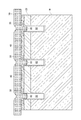
図1は、本発明の実施形態による半導体装置10の構成を示す断面図である。また、図2は、半導体装置10の上面図である。尚、図1に示す断面は、図2のA−A線に沿った断面に相当する。
FIG. 1 is a cross-sectional view showing the configuration of the
本実施形態による半導体装置10はショットキーバリアダイオードであり、図1に示すように、いずれも酸化ガリウム(β−Ga2O3)からなる半導体基板21及びエピタキシャル層22を含む半導体層20を備える。本発明においては、半導体層20を「酸化ガリウム基板」と総称することがある。半導体基板21及びエピタキシャル層22には、n型ドーパントとしてシリコン(Si)又はスズ(Sn)が導入されている。ドーパントの濃度は、エピタキシャル層22よりも半導体基板21の方が高く、これにより半導体基板21はn+層、エピタキシャル層22はn−層として機能する。
The
半導体層20は、XY面を構成する第1の電極形成面20aと、第1の電極形成面20aの反対側に位置しXY面を構成する第2の電極形成面20bと、XZ面又はYZ面を構成する4つの側面20cを有する。第1及び第2の電極形成面20a,20bは、β−Ga2O3の(001)面である。第1の電極形成面20aはエピタキシャル層22の上面によって構成され、第2の電極形成面20bは半導体基板21の下面によって構成される。第1の電極形成面20aと側面20cの境界は第1のエッジE1を構成し、第2の電極形成面20bと側面20cの境界は第2のエッジE2を構成する。
The
図1及び図2に示すように、第1の電極形成面20a及び側面20cには、SiO2、Si3N4、Al2O3、HfO2などからなる絶縁膜30が形成されている。絶縁膜30は、第1の電極形成面20aを覆う第1の部分31と、側面20cを覆う第2の部分32を含み、第1のエッジE1を覆うよう、第1の電極形成面20aから側面20cに亘って連続的に形成されている。絶縁膜30は例えば酸化シリコン(SiO2)からなり、その膜厚は300nm程度である。
As shown in FIGS. 1 and 2, an
絶縁膜30の第1の部分31は、第1の電極形成面20aを露出させる開口部30aを有している。そして、第1の電極形成面20a上には、開口部30aを介して第1の電極であるアノード電極40が形成されている。これにより、アノード電極40は、エピタキシャル層22とショットキー接触する。アノード電極40は、例えば白金(Pt)、チタン(Ti)及びアルミニウム(Al)の積層膜からなり、その膜厚は、例えば、白金層が50nm程度、チタン層が5nm程度、アルミニウム層が1μm程度である。
The
アノード電極40の大部分はエピタキシャル層22とショットキー接触するが、他の一部は絶縁膜30の第1の部分31を覆っている。これにより、いわゆるフィールドプレート構造が得られる。一般的に、ショットーバリアダイオードではアノード電極の端部に電界が集中するため、この部分が絶縁破壊電界強度を超えると素子が破壊されてしまう。しかしながら、本実施形態のようにアノード電極40の端部を絶縁膜30上に形成すれば、端部における電流集中が緩和されるため、逆方向耐圧を高めることができる。
Most of the
一方、半導体層20の第2の電極形成面20bには、第2の電極であるカソード電極50が設けられる。カソード電極50はチタン(Ti)、ニッケル(Ni)及び金(Au)の積層膜などからなり、半導体基板21とオーミック接触している。例えば、チタン層の厚さは50nm程度、ニッケル層の厚さは0.2μm程度、金層の厚さは0.2μm程度である。
On the other hand, a
以上の構成により、本実施形態による半導体装置10は、ショットキーバリアダイオードを構成する。ショットキーバリアダイオードはスイッチング素子に用いられ、アノード電極40とカソード電極50との間に順方向バイアスを印加することにより、アノード電極40とエピタキシャル層22の界面におけるショットキー障壁が低下し、アノード電極40からカソード電極50へ電流が流れる。一方、アノード電極40とカソード電極50間に逆方向バイアスを印加すると、アノード電極40とエピタキシャル層22の界面におけるショットキー障壁が高くなり、電流はほとんど流れない。
With the above configuration, the
そして、本実施形態による半導体装置10は、半導体層20の側面20cが絶縁膜で覆われていることから、側面20cに沿ったリーク電流が低減されるとともに、側面20cの割れ、欠け、劈開などが生じにくくなる。しかも、第1のエッジE1を覆うよう第1の電極形成面20aから側面20cに亘って絶縁膜30が連続的に形成されていることから、第1の電極形成面20aを覆う絶縁膜と側面20cを覆う絶縁膜をそれぞれ別個に形成する場合と比べて、上記の効果がより高められる。また、第1のエッジE1における酸化ガリウム基板の割れや欠けなども防止される。
In the
次に、本実施形態による半導体装置10の製造方法について説明する。
Next, a method of manufacturing the
図3は、本実施形態による半導体装置10の製造プロセスを示すフローチャートである。
FIG. 3 is a flowchart showing a manufacturing process of the
まず、図4に示すように、融液成長法などを用いて育成されたバルク結晶をスライスしてなる酸化ガリウムウェーハWを用意し、その表面にエピタキシャル層22を形成する。エピタキシャル層22は、酸化ガリウムウェーハWの表面に反応性スパッタリング、PLD法、MBE法、MOCVD法、HVPE法などを用いて酸化ガリウムをエピタキシャル成長させることにより形成することができる。エピタキシャル層22のキャリア濃度と膜厚は、設計に応じた耐圧を確保するよう調整される。一例として、600V程度の逆方向耐圧を得るためには、厚みを7〜8μm、キャリア濃度を1×1016cm−3程度とすればよい。キャリア濃度の制御は、Si、Snなどn型のキャリアとして機能するドーパントを所望の量だけ成膜時に導入することにより行う。これにより、酸化ガリウムウェーハWの表面にエピタキシャル層22が形成された酸化ガリウム基板が完成する(ステップS1)。
First, as shown in FIG. 4, a gallium oxide wafer W formed by slicing a bulk crystal grown by a melt growth method or the like is prepared, and an
次に、図5に示すように、エピタキシャル層22の表面である第1の電極形成面20aのうち、素子が形成される素子形成領域をエッチング用マスクM1で覆った状態でドライエッチングを行うことにより、酸化ガリウム基板に複数のスリット60を形成する(ステップS2)。スリット60は、エピタキシャル層22を貫通し、酸化ガリウムウェーハWに達する深さに設定する。具体的には、最終的な半導体層20の厚みよりも、スリット60の深さをやや深く設定する。例えば、最終的な半導体層20の厚みが50μmであれば、スリット60の深さを55μm程度に設定すればよい。
Next, as shown in FIG. 5, dry etching is performed in a state where the element forming region on which the element is formed is covered with the etching mask M1 in the first
スリット60の形成は、BCl3等の塩素系ガスを用いたRIE法によって行うことができる。特に、エッチング時間を短縮するためには、高速エッチングが可能なICP−RIE法を用いることが好ましい。エッチング用マスクM1としては、例えばGa2O3に対して選択性をもたせるため、塩素系ガスでエッチングされないニッケル(Ni)などの金属膜を使用することが好ましい。この場合、エッチング用マスクM1である金属膜は、EB蒸着法、スパッタ法などを用いて100nm程度形成すれば良く、エピタキシャル層22の全面にエッチング用マスクM1を形成した後、フォトリソグラフィー法によってパターニングすればよい。そして、パターニングされたエッチング用マスクM1をマスクとしてドライエッチングを行うことにより、酸化ガリウム基板に複数のスリット60が形成される。
The
スリット60は、平面図である図6(a)に示すようにX方向及びY方向に複数形成され、平面視でスリット60に囲まれた矩形領域が最終的に素子となる部分である。図6(b)は、図6(a)に示すB−B線に沿った略断面図である。一例として、素子サイズを1mm×1mmとする場合、幅が20μmであるスリット60を1.02mmピッチでX方向及びY方向に形成すればよい。スリット60を形成した後は、一般的な酸系エッチング液を用いてエッチング用マスクM1を除去し、基板洗浄を行う。
As shown in FIG. 6A, which is a plan view, a plurality of
このようにして形成されたスリット60は、ダイシングブレードなどを用いた機械加工によるものとは異なり、内壁61にほとんどダメージが生じない。また、内壁61の平坦性も非常に高く、具体的には凹凸が1μm以下であり、その表面性もほぼ均一となる。
The
次に、図7に示すように、エピタキシャル層22の表面及びスリット60の内壁61に、SiO2、Si3N4、Al2O3、HfO2などからなる絶縁膜30を形成する(ステップS3)。絶縁膜30の形成方法は、ALD法やCVD法などのカバレッジに優れた成膜方法を用いることが好ましく、これによりエピタキシャル層22の表面だけでなく、スリット60の内壁61のほぼ全面が絶縁膜30で覆われる。また、スリット60の開口部である第1のエッジE1部分も絶縁膜30で覆われる。絶縁膜30は複数の成膜方法を組み合わせて積層してもよい。
Next, as shown in FIG. 7, an insulating
次に、図8に示すように、絶縁膜30に開口部30aを形成した後、図9に示すように、アノード電極40を形成する(ステップS4)。開口部30aの形成は、通常のフォトリソグラフィー法によってレジストをパターニングした後、レジストをマスクとして絶縁膜30をドライエッチング又はウェットエッチングすればよい。但し、この時点で酸化ガリウム基板には複数のスリット60が形成されていることから、レジストとしては塗布型の液体レジストよりも、フィルムタイプの固体レジストを用いることが好ましい。
Next, as shown in FIG. 8, after forming the
アノード電極40は蒸着法によって形成することができ、リフトオフ工程を用いてパターニングすることができる。つまり、まず絶縁膜30の開口部30aよりも平面サイズが5μm程度大きいレジストパターンを形成した後、蒸着法により白金(Pt)を50nm、チタン(Ti)を5nm、アルミニウム(Al)を1μm程度形成する。そして、レジストパターンを除去すれば、レジストパターン上の金属層をレジストパターンごと除去することができる。ここで、スリット60内への金属膜の付着を抑えるためには、フィルムタイプの固体レジストを用いることが好ましい。或いは、全面に形成したアノード電極40をパターニングするのではなく、格子状の金属マスクなどを介して蒸着を行うことにより、アノード電極40を選択的に成膜しても構わない。但し、本実施形態においては、スリット60の内壁61が絶縁膜30で覆われていることから、僅かな金属材料がスリット60内に侵入しても、これが酸化ガリウム基板と接することはない。
The
次に、図10に示すように、酸化ガリウム基板の表面に可撓性を有する支持部材70を貼り付ける(ステップS5)。可撓性を有する支持部材70としては、厚手の樹脂フィルムのような柔軟性の高い部材を用いることが好ましい。このような柔軟性の高い支持部材70を酸化ガリウム基板の表面に貼り付けた後、ある程度の圧力を加えれば、支持部材70が変形し、その一部がスリット60に埋め込まれた保護部材80となる。この保護部材80により、アノード電極40がスリット60から空間的に遮蔽される。
Next, as shown in FIG. 10, a
次に、図11に示すように、酸化ガリウム基板を支持部材70によって支持した状態で、裏面側、つまり酸化ガリウムウェーハWの下面の研削及び研磨を行う(ステップS6)。研削及び研磨は、通常のシリコン基板の研削及び研磨と同様の方法で行うことができる。酸化ガリウムウェーハWの研削及び研磨はスリット60に達するまで行い、これにより、半導体基板21及びエピタキシャル層22からなる酸化ガリウム基板が複数個に個片化される。研削及び研磨を行った後は、洗浄を行うことにより研磨面を清浄化する。尚、研削を行うことなく、研磨のみによって個片化しても構わない。
Next, as shown in FIG. 11, in a state where the gallium oxide substrate is supported by the
次に、図12に示すように、酸化ガリウムからなる半導体基板21の下面にカソード電極50を形成する(ステップS7)。カソード電極50は、蒸着法やスパッタ法など、カバレッジ性の低い薄膜工法を用いて形成することが好ましい。これによれば、半導体基板21の下面にはカソード電極50が正しく成膜される一方、スリット60の内壁61には電極材料がほとんど回り込まないため、内壁61にはほとんど電極が形成されない。カソード電極50の電極材料は、一部がスリット60内に侵入するが、図12に示すように、スリット60の上部は支持部材70の一部からなる保護部材80で埋め込まれていることから、カソード電極50の電極材料がアノード電極40に達することはない。スリット60内への電極材料の侵入を防止するためには、格子状の金属マスクなどによってスリット60を覆った状態で蒸着などを行うことにより、カソード電極50を半導体基板21の下面に選択的に成膜することが好ましい。
Next, as shown in FIG. 12, the
そして、図13に示すように、支持部材70を剥離すれば複数の半導体装置10の作製が完了する(ステップS8)。個片化された半導体装置10は、必要に応じてパッケージに搭載される。パッケージは銅(Cu)などからなるベースプレートを有しており、半田を介してベースプレートと半導体装置10のカソード電極50が接続される。半導体装置10のアノード電極40は、ボンディングワイヤを介してパッケージのリードフレームに接続される。
Then, as shown in FIG. 13, if the
このように、本実施形態による半導体装置10の製造方法によれば、ドライエッチングによって酸化ガリウム基板の上面側に複数のスリット60を形成した後、酸化ガリウム基板の下面側を研削及び研磨することによって個片化していることから、半導体層20の側面20cが機械的ダメージを受けない。このため、ダイシングブレードなどを用いて個片化する場合とは異なり、側面20cに割れ、欠け、劈開などが生じない。特に、β−Ga2O3は、(100)面と(001)面が劈開性を有しているため、電極形成面20a,20bがβ−Ga2O3の(001)面である場合、ダイシングブレードなどを用いて個片化すると、側面20cには水平方向に多数の劈開が生じることがある。このような劈開が生じると、デバイス特性が変化するおそれがあるだけでなく、劈開によって生じた酸化ガリウム粉が飛散するおそれがある。しかしながら、本実施形態による半導体装置10の製造方法によれば、側面20cがドライエッチングによって形成された面であることから、このような劈開はほとんど生じない。仮に僅かな劈開などが生じても、側面20cが絶縁膜30で覆われていることから、酸化ガリウム粉が飛散することもない。また、酸化ガリウムは熱伝導率が低いため、順方向電流による発熱が素子の外部に効率的に放熱されず、素子が劣化しやすいという問題がある。しかしながら、本実施形態においては、酸化ガリウムウェーハWの裏面を研磨することによって半導体層20を薄型化していることから、放熱性を高めることも可能となる。
As described above, according to the method for manufacturing the
しかも、フィールドプレート構造を得るための絶縁膜30を形成する際、スリット60の内壁61にも絶縁膜30が同時に形成されることから、工程数を増やすことなく、第1の電極形成面20aとスリット60の内壁61の両方に絶縁膜30を形成することができる。このように、第1の電極形成面20aに形成される絶縁膜30(第1の部分31)と側面20cに形成される絶縁膜30(第2の部分32)は同時に形成されることから、両者間に継ぎ目などが無い。このため、側面20cに沿ったリーク電流を効果的に抑制することが可能となる。
Moreover, when the insulating
尚、上述した製造方法では、可撓性を有する支持部材70を用いることによって、支持部材70の一部からなる保護部材80をスリット60の上部に埋め込んでいるが、リジッドな支持部材70や可撓性の低い支持部材70を用いる場合には、図14に示すように、スリット60を形成した後、酸化ガリウム基板を個片化する前に、支持部材70とは別の保護部材80をスリット60に埋め込んでも構わない。また、保護部材80の埋め込みは、酸化ガリウム基板を個片化した後、カソード電極50を形成する前に行っても構わない。いずれにしても、カソード電極50を形成する際に保護部材80がスリット60に埋め込まれていれば、カソード電極50の電極材料がスリット60に侵入しても、この電極材料がアノード電極40に達することはない。
In the manufacturing method described above, by using the
また、スリット60を形成する工程(ステップS2)においては、ドライエッチングの条件を調整することによって、図15に示すように順テーパー状のスリット60を形成しても構わない。順テーパーとは、スリット幅が深さ方向に徐々に狭くなる形状を指す。これによれば、絶縁膜30を形成する工程(ステップS3)において、絶縁膜30がスリット60の内壁61に形成され易くなるという利点が得られる。このような順テーパー状のスリット60を形成した場合、最終的に得られる半導体装置10の形状は、図16に示すように、半導体層20のXY断面が第1の電極形成面20aから第2の電極形成面20bに向かって拡大するテーパー形状となる。このような形状は、パッケージ上における搭載安定性に寄与する。
Further, in the step of forming the slit 60 (step S2), the
以上、本発明の好ましい実施形態について説明したが、本発明は、上記の実施形態に限定されることなく、本発明の主旨を逸脱しない範囲で種々の変更が可能であり、それらも本発明の範囲内に包含されるものであることはいうまでもない。 Although the preferred embodiments of the present invention have been described above, the present invention is not limited to the above embodiments, and various modifications can be made without departing from the gist of the present invention, and these are also the present invention. It goes without saying that it is included in the range.
例えば、上記実施形態では、本発明をショットキーバリアダイオードに適用した場合を例に説明したが、本発明がこれに限定されるものではなく、電流が基板の厚み方向に流れる縦型の半導体装置であれば、他の種類の半導体装置に応用することも可能である。 For example, in the above embodiment, the case where the present invention is applied to a Schottky barrier diode has been described as an example, but the present invention is not limited to this, and a vertical semiconductor device in which a current flows in the thickness direction of the substrate. If so, it can be applied to other types of semiconductor devices.
また、上記実施形態では、半導体層の材料として酸化ガリウムを用いているが、本発明がこれに限定されるものではない。 Further, in the above embodiment, gallium oxide is used as the material of the semiconductor layer, but the present invention is not limited thereto.
10 半導体装置
20 半導体層
20a 第1の電極形成面
20b 第2の電極形成面
20c 側面
21 半導体基板
22 エピタキシャル層
30 絶縁膜
30a 開口部
31 第1の部分
32 第2の部分
40 アノード電極
50 カソード電極
60 スリット
61 内壁
70 支持部材
80 保護部材
E1 第1のエッジ
E2 第2のエッジ
M1 エッチング用マスク
W 酸化ガリウムウェーハ
10
Claims (8)
前記第1の電極形成面に形成された第1の電極と、
前記第2の電極形成面に形成された第2の電極と、
前記第1のエッジを覆うよう、前記第1の電極形成面から前記側面に亘って連続的に形成された絶縁膜と、を備え、
前記半導体層の前記側面は、露出することなく前記絶縁膜によって全面が覆われ、
前記第2の電極の側面は、前記絶縁膜によって覆われることなく露出していることを特徴とする半導体装置。 The first edge and the second edge, which are the boundaries between the first electrode forming surface, the second electrode forming surface located on the opposite side of the first electrode forming surface, and the first electrode forming surface. A semiconductor layer having a side surface having a second edge, which is a boundary with the electrode forming surface, and
With the first electrode formed on the first electrode forming surface,
With the second electrode formed on the second electrode forming surface,
An insulating film continuously formed from the first electrode forming surface to the side surface is provided so as to cover the first edge .
The side surface of the semiconductor layer is entirely covered with the insulating film without being exposed.
A semiconductor device characterized in that the side surface of the second electrode is exposed without being covered with the insulating film .
前記第1の電極の少なくとも一部は前記エピタキシャル層とショットキー接触し、前記第2の電極は前記半導体基板とオーミック接触すること特徴とする請求項1に記載の半導体装置。 The semiconductor layer includes a semiconductor substrate forming the second electrode forming surface and an epitaxial layer provided on the semiconductor substrate and forming the first electrode forming surface.
The semiconductor device according to claim 1, wherein at least a part of the first electrode is in Schottky contact with the epitaxial layer, and the second electrode is in ohmic contact with the semiconductor substrate.
前記エピタキシャル層を貫通し、前記酸化ガリウムウェーハに達する深さのスリットを形成する第2の工程と、
前記スリットの開口部であるエッジが覆われるよう、前記エピタキシャル層の表面及び前記スリットの内壁に絶縁膜を形成する第3の工程と、
前記絶縁膜に開口部を形成することによって前記エピタキシャル層の表面を露出させた後、前記エピタキシャル層と接するアノード電極を形成する第4の工程と、
前記第4の工程を行った後、前記スリットに達するまで前記酸化ガリウムウェーハの下面を研磨することによって個片化する第5の工程と、
前記第5の工程を行った後、前記酸化ガリウムウェーハの下面にカソード電極を形成する第6の工程と、を備えることを特徴とする半導体装置の製造方法。
The first step of forming an epitaxial layer on the surface of a gallium oxide wafer,
A second step of penetrating the epitaxial layer and forming a slit having a depth reaching the gallium oxide wafer.
A third step of forming an insulating film on the surface of the epitaxial layer and the inner wall of the slit so as to cover the edge which is the opening of the slit.
A fourth step of forming an anode electrode in contact with the epitaxial layer after exposing the surface of the epitaxial layer by forming an opening in the insulating film.
After performing the fourth step, the fifth step of polishing the lower surface of the gallium oxide wafer to individualize it until it reaches the slit, and the fifth step.
A method for manufacturing a semiconductor device, which comprises a sixth step of forming a cathode electrode on the lower surface of the gallium oxide wafer after performing the fifth step.
Priority Applications (5)
| Application Number | Priority Date | Filing Date | Title |
|---|---|---|---|
| JP2017064123A JP6809334B2 (en) | 2017-03-29 | 2017-03-29 | Semiconductor devices and their manufacturing methods |
| US16/496,715 US11164953B2 (en) | 2017-03-29 | 2018-01-26 | Semiconductor device |
| PCT/JP2018/002438 WO2018179768A1 (en) | 2017-03-29 | 2018-01-26 | Semiconductor device |
| EP18778040.8A EP3608972B1 (en) | 2017-03-29 | 2018-01-26 | Semiconductor device |
| CN201880022742.0A CN110521004B (en) | 2017-03-29 | 2018-01-26 | Semiconductor device |
Applications Claiming Priority (1)
| Application Number | Priority Date | Filing Date | Title |
|---|---|---|---|
| JP2017064123A JP6809334B2 (en) | 2017-03-29 | 2017-03-29 | Semiconductor devices and their manufacturing methods |
Publications (2)
| Publication Number | Publication Date |
|---|---|
| JP2018170305A JP2018170305A (en) | 2018-11-01 |
| JP6809334B2 true JP6809334B2 (en) | 2021-01-06 |
Family
ID=63674938
Family Applications (1)
| Application Number | Title | Priority Date | Filing Date |
|---|---|---|---|
| JP2017064123A Active JP6809334B2 (en) | 2017-03-29 | 2017-03-29 | Semiconductor devices and their manufacturing methods |
Country Status (5)
| Country | Link |
|---|---|
| US (1) | US11164953B2 (en) |
| EP (1) | EP3608972B1 (en) |
| JP (1) | JP6809334B2 (en) |
| CN (1) | CN110521004B (en) |
| WO (1) | WO2018179768A1 (en) |
Families Citing this family (6)
| Publication number | Priority date | Publication date | Assignee | Title |
|---|---|---|---|---|
| US10971634B2 (en) * | 2017-06-29 | 2021-04-06 | Mitsubishi Electric Corporation | Oxide semiconductor device and method of manufacturing oxide semiconductor device |
| JP7279354B2 (en) * | 2018-12-17 | 2023-05-23 | 富士電機株式会社 | Semiconductor device and method for identifying semiconductor device |
| JP7391326B2 (en) * | 2019-12-26 | 2023-12-05 | 株式会社ノベルクリスタルテクノロジー | semiconductor equipment |
| CN111540788A (en) * | 2020-06-18 | 2020-08-14 | 中国科学院半导体研究所 | Schottky diode and preparation method thereof |
| US12198998B2 (en) * | 2021-12-09 | 2025-01-14 | Nxp B.V. | Dielectric sidewall protection and sealing for semiconductor devices in a in wafer level packaging process |
| CN114497234B (en) * | 2022-01-25 | 2022-12-06 | 先之科半导体科技(东莞)有限公司 | Low-loss small-volume Schottky diode |
Family Cites Families (10)
| Publication number | Priority date | Publication date | Assignee | Title |
|---|---|---|---|---|
| JPH09116133A (en) * | 1995-10-13 | 1997-05-02 | Toyo Electric Mfg Co Ltd | High voltage semiconductor device |
| JP2002353227A (en) | 2001-05-28 | 2002-12-06 | Sanken Electric Co Ltd | Semiconductor device |
| JP2004119472A (en) * | 2002-09-24 | 2004-04-15 | Seiko Epson Corp | Semiconductor device and its manufacturing method, circuit board, and electronic equipment |
| JP4697397B2 (en) * | 2005-02-16 | 2011-06-08 | サンケン電気株式会社 | Composite semiconductor device |
| JP4945969B2 (en) * | 2005-09-07 | 2012-06-06 | 横河電機株式会社 | Semiconductor device and manufacturing method of semiconductor device |
| JP2009267032A (en) * | 2008-04-24 | 2009-11-12 | Toyota Motor Corp | Semiconductor device and manufacturing method thereof |
| JP2013102081A (en) * | 2011-11-09 | 2013-05-23 | Tamura Seisakusho Co Ltd | Schottky barrier diode |
| JP5914060B2 (en) * | 2012-03-09 | 2016-05-11 | 三菱電機株式会社 | Method for manufacturing silicon carbide semiconductor device |
| JP2014107499A (en) * | 2012-11-29 | 2014-06-09 | Sumitomo Electric Ind Ltd | Silicon carbide semiconductor device and method for manufacturing the same |
| JP2014225557A (en) * | 2013-05-16 | 2014-12-04 | 住友電気工業株式会社 | Method of manufacturing silicon carbide semiconductor device and semiconductor module, and silicon carbide semiconductor device and semiconductor module |
-
2017
- 2017-03-29 JP JP2017064123A patent/JP6809334B2/en active Active
-
2018
- 2018-01-26 EP EP18778040.8A patent/EP3608972B1/en active Active
- 2018-01-26 CN CN201880022742.0A patent/CN110521004B/en active Active
- 2018-01-26 WO PCT/JP2018/002438 patent/WO2018179768A1/en unknown
- 2018-01-26 US US16/496,715 patent/US11164953B2/en active Active
Also Published As
| Publication number | Publication date |
|---|---|
| US11164953B2 (en) | 2021-11-02 |
| WO2018179768A1 (en) | 2018-10-04 |
| EP3608972A1 (en) | 2020-02-12 |
| JP2018170305A (en) | 2018-11-01 |
| CN110521004A (en) | 2019-11-29 |
| EP3608972A4 (en) | 2020-12-16 |
| CN110521004B (en) | 2023-01-10 |
| EP3608972B1 (en) | 2024-03-20 |
| US20200111882A1 (en) | 2020-04-09 |
Similar Documents
| Publication | Publication Date | Title |
|---|---|---|
| JP6809334B2 (en) | Semiconductor devices and their manufacturing methods | |
| KR20140133944A (en) | III-nitride semiconductor vertical structure LED chip and manufacturing method thereof | |
| US8859315B2 (en) | Epitaxial wafer and manufacturing method thereof | |
| JP5774712B2 (en) | Semiconductor device and manufacturing method thereof | |
| KR101841631B1 (en) | High electron mobility transistor and fabrication method thereof | |
| JP6794896B2 (en) | Manufacturing method of gallium oxide semiconductor device | |
| CN113939918A (en) | Semiconductor device and method of manufacturing the same | |
| US9257574B2 (en) | Diode and method of manufacturing diode | |
| US20150200265A1 (en) | Solder-containing semiconductor device, mounted solder-containing semiconductor device, producing method and mounting method of solder-containing semiconductor device | |
| CN108788473B (en) | Compound semiconductor device, method for manufacturing the same, and resin-sealed semiconductor device | |
| WO2023095396A1 (en) | Junction barrier schottky diode | |
| JP2010177353A (en) | Method for producing gallium nitride based semiconductor electronic device | |
| TWI797493B (en) | Schottky barrier diode | |
| TWI860747B (en) | Schottky barrier diode | |
| KR20070044099A (en) | Nitride Semiconductor Light Emitting Diode and Manufacturing Method Thereof | |
| US20230030874A1 (en) | Semiconductor element, method for manufacturing semiconductor element, semiconductor device, and method for manufacturing semiconductor device | |
| TWI570957B (en) | Method for manufacturing semiconductor light emitting device | |
| KR102526716B1 (en) | Galliumnitride-based junction field effect transistor and manufacturing method thereof | |
| TW202201804A (en) | Schottky barrier diode | |
| WO2024190023A1 (en) | Schottky barrier diode | |
| KR101432908B1 (en) | Semiconductor substrate and method of manufacturing a semiconductor device having the same | |
| CN104798182A (en) | Schottky barrier diode and method for manufacturing same |
Legal Events
| Date | Code | Title | Description |
|---|---|---|---|
| A621 | Written request for application examination |
Free format text: JAPANESE INTERMEDIATE CODE: A621 Effective date: 20191212 |
|
| A131 | Notification of reasons for refusal |
Free format text: JAPANESE INTERMEDIATE CODE: A131 Effective date: 20200804 |
|
| A521 | Request for written amendment filed |
Free format text: JAPANESE INTERMEDIATE CODE: A523 Effective date: 20200928 |
|
| A131 | Notification of reasons for refusal |
Free format text: JAPANESE INTERMEDIATE CODE: A131 Effective date: 20201027 |
|
| A521 | Request for written amendment filed |
Free format text: JAPANESE INTERMEDIATE CODE: A523 Effective date: 20201029 |
|
| TRDD | Decision of grant or rejection written | ||
| A01 | Written decision to grant a patent or to grant a registration (utility model) |
Free format text: JAPANESE INTERMEDIATE CODE: A01 Effective date: 20201110 |
|
| A61 | First payment of annual fees (during grant procedure) |
Free format text: JAPANESE INTERMEDIATE CODE: A61 Effective date: 20201123 |
|
| R150 | Certificate of patent or registration of utility model |
Ref document number: 6809334 Country of ref document: JP Free format text: JAPANESE INTERMEDIATE CODE: R150 |
|
| R250 | Receipt of annual fees |
Free format text: JAPANESE INTERMEDIATE CODE: R250 |