JP6566889B2 - contact - Google Patents
contact Download PDFInfo
- Publication number
- JP6566889B2 JP6566889B2 JP2016027854A JP2016027854A JP6566889B2 JP 6566889 B2 JP6566889 B2 JP 6566889B2 JP 2016027854 A JP2016027854 A JP 2016027854A JP 2016027854 A JP2016027854 A JP 2016027854A JP 6566889 B2 JP6566889 B2 JP 6566889B2
- Authority
- JP
- Japan
- Prior art keywords
- press
- circuit board
- fit
- contact
- hole
- Prior art date
- Legal status (The legal status is an assumption and is not a legal conclusion. Google has not performed a legal analysis and makes no representation as to the accuracy of the status listed.)
- Active
Links
- 238000010586 diagram Methods 0.000 description 3
- 239000011347 resin Substances 0.000 description 3
- 229920005989 resin Polymers 0.000 description 3
- 238000004904 shortening Methods 0.000 description 3
- 230000009466 transformation Effects 0.000 description 3
- 239000004020 conductor Substances 0.000 description 2
- 238000000034 method Methods 0.000 description 2
- 230000008054 signal transmission Effects 0.000 description 2
- 238000005452 bending Methods 0.000 description 1
- 230000005540 biological transmission Effects 0.000 description 1
- 230000015572 biosynthetic process Effects 0.000 description 1
- 238000010276 construction Methods 0.000 description 1
- 238000003780 insertion Methods 0.000 description 1
- 230000037431 insertion Effects 0.000 description 1
- 239000012212 insulator Substances 0.000 description 1
- 238000004519 manufacturing process Methods 0.000 description 1
- 239000000463 material Substances 0.000 description 1
- 238000000465 moulding Methods 0.000 description 1
- 238000003825 pressing Methods 0.000 description 1
- 238000004080 punching Methods 0.000 description 1
- 239000000758 substrate Substances 0.000 description 1
Images


Classifications
-
- H—ELECTRICITY
- H01—ELECTRIC ELEMENTS
- H01R—ELECTRICALLY-CONDUCTIVE CONNECTIONS; STRUCTURAL ASSOCIATIONS OF A PLURALITY OF MUTUALLY-INSULATED ELECTRICAL CONNECTING ELEMENTS; COUPLING DEVICES; CURRENT COLLECTORS
- H01R13/00—Details of coupling devices of the kinds covered by groups H01R12/70 or H01R24/00 - H01R33/00
- H01R13/02—Contact members
- H01R13/22—Contacts for co-operating by abutting
- H01R13/24—Contacts for co-operating by abutting resilient; resiliently-mounted
- H01R13/2435—Contacts for co-operating by abutting resilient; resiliently-mounted with opposite contact points, e.g. C beam
-
- H—ELECTRICITY
- H01—ELECTRIC ELEMENTS
- H01R—ELECTRICALLY-CONDUCTIVE CONNECTIONS; STRUCTURAL ASSOCIATIONS OF A PLURALITY OF MUTUALLY-INSULATED ELECTRICAL CONNECTING ELEMENTS; COUPLING DEVICES; CURRENT COLLECTORS
- H01R12/00—Structural associations of a plurality of mutually-insulated electrical connecting elements, specially adapted for printed circuits, e.g. printed circuit boards [PCB], flat or ribbon cables, or like generally planar structures, e.g. terminal strips, terminal blocks; Coupling devices specially adapted for printed circuits, flat or ribbon cables, or like generally planar structures; Terminals specially adapted for contact with, or insertion into, printed circuits, flat or ribbon cables, or like generally planar structures
- H01R12/50—Fixed connections
- H01R12/51—Fixed connections for rigid printed circuits or like structures
- H01R12/55—Fixed connections for rigid printed circuits or like structures characterised by the terminals
- H01R12/58—Fixed connections for rigid printed circuits or like structures characterised by the terminals terminals for insertion into holes
- H01R12/585—Terminals having a press fit or a compliant portion and a shank passing through a hole in the printed circuit board
-
- H—ELECTRICITY
- H01—ELECTRIC ELEMENTS
- H01R—ELECTRICALLY-CONDUCTIVE CONNECTIONS; STRUCTURAL ASSOCIATIONS OF A PLURALITY OF MUTUALLY-INSULATED ELECTRICAL CONNECTING ELEMENTS; COUPLING DEVICES; CURRENT COLLECTORS
- H01R13/00—Details of coupling devices of the kinds covered by groups H01R12/70 or H01R24/00 - H01R33/00
- H01R13/02—Contact members
- H01R13/04—Pins or blades for co-operation with sockets
- H01R13/05—Resilient pins or blades
-
- H—ELECTRICITY
- H01—ELECTRIC ELEMENTS
- H01R—ELECTRICALLY-CONDUCTIVE CONNECTIONS; STRUCTURAL ASSOCIATIONS OF A PLURALITY OF MUTUALLY-INSULATED ELECTRICAL CONNECTING ELEMENTS; COUPLING DEVICES; CURRENT COLLECTORS
- H01R4/00—Electrically-conductive connections between two or more conductive members in direct contact, i.e. touching one another; Means for effecting or maintaining such contact; Electrically-conductive connections having two or more spaced connecting locations for conductors and using contact members penetrating insulation
- H01R4/10—Electrically-conductive connections between two or more conductive members in direct contact, i.e. touching one another; Means for effecting or maintaining such contact; Electrically-conductive connections having two or more spaced connecting locations for conductors and using contact members penetrating insulation effected solely by twisting, wrapping, bending, crimping, or other permanent deformation
Landscapes
- Coupling Device And Connection With Printed Circuit (AREA)
- Multi-Conductor Connections (AREA)
Description
本発明は、回路基板のスルーホールに圧入されて回路基板に形成された配線等と電気的に接続するコンタクトに関する。 The present invention relates to a contact that is press-fitted into a through hole of a circuit board and is electrically connected to wiring or the like formed on the circuit board.
従来より、回路基板のスルーホールに圧入される、いわゆるプレスフィットコンタクトと称されるコンタクトが知られている。 Conventionally, a so-called press-fit contact that is press-fitted into a through hole of a circuit board is known.
特許文献1の図5には、回路基板のスルーホールに圧入された状態のプレスフィットコンタクトが示されている。この図5においてスルーホールに圧入されたプレスフィットコンタクトは、回路基板に埋め込まれた配線層と電気的に導通している。ただし、プレスフィットコンタクトの圧入された部分の先端及びスルーホールは、そのスルーホールが導通している配線層の深さよりも深い位置まで達している。この構造を高速信号伝送用として使用すると、プレスフィットコンタクトの、導通している配線層よりも深く差し込まれている部分で信号の反射が発生して信号が乱れる。したがって、プレスフィットコンタクトが導通している配線層よりもスルーホールが長い場合や、プレスフィットコンタクトがその配線層よりも深くまで差し込まれている構造は、高速伝送信号の品質を下げる原因になる。このため、回路基板のプレスフィットコンタクトが挿入される面と反対側の面からドリルで削除してスルーホールを短くしたり、プレスフィットコンタクト自体を短くする対策がとられてきた。 FIG. 5 of Patent Document 1 shows a press-fit contact in a state of being press-fitted into a through hole of a circuit board. In FIG. 5, the press-fit contact press-fitted into the through hole is electrically connected to the wiring layer embedded in the circuit board. However, the tip of the press-fit contact and the through hole reach a position deeper than the depth of the wiring layer through which the through hole is conducted. When this structure is used for high-speed signal transmission, signal reflection occurs at the portion of the press-fit contact that is inserted deeper than the conductive wiring layer, and the signal is disturbed. Therefore, the case where the through hole is longer than the wiring layer in which the press-fit contact is conducted or the structure in which the press-fit contact is inserted deeper than the wiring layer causes the quality of the high-speed transmission signal to be lowered. For this reason, measures have been taken to shorten the through-holes by shortening the through-holes by shortening the through-holes by removing them from the surface of the circuit board opposite to the surface where the press-fit contacts are inserted.
ここで、特許文献1では、導電体と絶縁体とを組み合わせ、回路基板のスルーホールを突き抜ける長さとすることで、この問題を解決しようとしている。しかしながら、このようなプレスフィットコンタクトを製造するにはインサート成形等を必要とし、コスト高となるおそれがある。 Here, in patent document 1, it is going to solve this problem by combining a conductor and an insulator and making it the length which penetrates the through hole of a circuit board. However, manufacturing such a press-fit contact requires insert molding or the like, which may increase the cost.
そこで、このプレスフィットコンタクトの圧入される部分を単純に短くすることを考える。特許文献1に示されているように、このプレスフィットコンタクトの圧入される部分には開口部が存在する。プレスフィットコンタクトはその開口部を狭くしながら圧入される。圧入される部分がある程度の長さを有する場合は、その開口部の位置の公差等、プレスフィットコンタクトの各部の公差にも余裕がある。しかしながら、プレスフィットコンタクトの、スルーホールに挿し込まれる部分の長さが、例えば0.4mmなど極端に短いと、公差が厳しくなり、スルーホール内におけるプレスフィット部の高精度の位置決めが困難になる。 Accordingly, consider simply shortening the press-fitted portion of the press-fit contact. As shown in Patent Document 1, an opening exists in the press-fit contact of the press-fit contact. The press-fit contact is press-fitted while narrowing the opening. When the portion to be press-fitted has a certain length, there is a margin in the tolerance of each part of the press-fit contact, such as the tolerance of the position of the opening. However, if the length of the portion of the press-fit contact that is inserted into the through hole is extremely short, such as 0.4 mm, the tolerance becomes severe, and it becomes difficult to position the press fit portion in the through hole with high accuracy. .
本発明は、上記事情に鑑み、スルーホールへの圧入長が短くてもプレスフィット部の高精度な位置決めを可能としたコンタクトを提供することを目的とする。 In view of the above circumstances, an object of the present invention is to provide a contact that enables highly accurate positioning of a press-fit portion even if the press-fitting length into a through hole is short.
上記目的を達成する本発明のコンタクトは、
回路基板のスルーホールに圧入されるプレスフィット部と、
プレスフィット部の、スルーホールへの圧入の向きの後方に位置して塑性変形する変形部と、
変形部の、プレスフィット部との境界部分に、プレスフィット部圧入側の回路基板の表面に当接するストッパ部とを備え、
プレスフィット部をスルーホールに対面させて変形部よりも後方の位置から回路基板に向けて荷重を加えたときに、変形部が、プレスフィット部がスルーホールに圧入される荷重では塑性変形を免れてプレスフィット部が圧入されるよりも大きな荷重を加えたときに塑性変形し、ストッパ部が、変形部が塑性変形してもなお回路基板の表面に当接し続ける荷重領域が存在する形状を有することを特徴とする。
The contact of the present invention that achieves the above object is:
And a press-fit portion to be press-fitted into the through-hole of the circuit board,
Of the press-fit part, and the deformation part for 塑 deformation is located at the rear of the direction of the press-fit to the through-hole,
Provided at the boundary part of the deformed part with the press fit part is a stopper part that comes into contact with the surface of the circuit board on the press fit part press-fitting side,
When a load is applied to the circuit board from a position behind the deformed portion with the press fit portion facing the through hole, the deformed portion is free from plastic deformation when the press fit portion is press-fitted into the through hole. The press-fit part is plastically deformed when a larger load is applied than the press-fit part is pressed, and the stopper part has a shape in which there is a load region that continues to contact the surface of the circuit board even if the deformed part is plastically deformed. It is characterized by that.
ここで、本発明のコンタクトの場合、上記変形部は、プレスフィット部がスルーホールに圧入されるのに要する荷重よりも大きな荷重を受けたときに塑性変形する強さを有する。
In the case of the contact of the present invention, the deformable portion, that have a strength that plastic deformation when the press-fit portion is subjected to a large load than the load required to be press-fitted into the through-hole.
また、本発明のコンタクトは、上記変形部の、プレスフィット部との境界部分に、プレスフィット部圧入側の回路基板の表面に当接するストッパ部を有する。
The contact of the present invention, the deformable portion, the boundary between the press-fit portion, that have a contact with the stopper portion on the surface of the circuit board of the press-fit portion press-fitting side.
本発明のコンタクトは、上記のストッパ部を備えているため、変形部へのスルーホールの入り込みが確実に防止される。
Contacts of the present invention is provided with the stopper portion of the, entry of the through hole of the deformable portion can be reliably prevented.
ここで、本発明のコンタクトにおいて、プレスフィット部および変形部は、連続した1 枚の平板形状を有することが好ましい。
Here, in the contact according to the present invention, it is preferable that the press-fit portion and the deformed portion have a continuous flat plate shape.
また、本発明のコンタクトにおいて、上記回路基板が、その回路基板の厚み内に複数の配線層が埋め込まれた回路基板であって、上記プレスフィット部が、その回路基板に埋め込まれた複数の配線層のうちの最も浅い配線層との間の電気接続を担うことが好ましい。
In the contact of the present invention, the circuit board is a circuit board in which a plurality of wiring layers are embedded within the thickness of the circuit board, and the press-fit portion is a plurality of wirings embedded in the circuit board. It is preferable to provide electrical connection with the shallowest wiring layer of the layers.
本発明のコンタクトは、圧入長が短い場合に特に有効であり、回路基板に埋め込まれた複数の配線層のうちの最も浅い配線層との間の電気接続用として好適である。 The contact of the present invention is particularly effective when the press-fitting length is short, and is suitable for electrical connection with the shallowest wiring layer among a plurality of wiring layers embedded in a circuit board.
以上の本発明によれば、圧入長が短い場合であってもプレスフィット部の高精度の位置決めが可能となる。 According to the present invention described above, the press-fit portion can be positioned with high accuracy even when the press-fitting length is short.
以下、本発明の実施の形態について説明する。 Embodiments of the present invention will be described below.
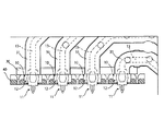
図1は、いわゆるチクレットと称される、主回路基板と子回路基板とを電気的に接続する部品の、子回路基板との接続部近傍の主要構成要素を示した図である。 FIG. 1 is a diagram showing main components in the vicinity of a connection portion between a main circuit board and a sub circuit board, which are called so-called chiclets, in the vicinity of a connection portion with the sub circuit board.
この図1には、4つ並んだ状態の、本実施形態に特徴的なコンタクト10が示されている。これらのコンタクト10は、樹脂製のハウジング30に支持されている。これらのコンタクト10は、プレスフィット部11と変形部12とを有する。プレスフィット部11は、上方からの荷重を受けて、子回路基板20のスルーホール21(図2参照)に圧入される。すなわち、このコンタクト10は子回路基板20との接続を担っている。プレスフィット部11と変形部12の詳細については後述する。
FIG. 1 shows four
また、ここには、整列板40が備えられている。この整列板40は、ハウジング30に対し図1の上下方向に可動式となっている。この図1には、上方に移動した状態の整列板40が示されている。この整列板40は、子回路基板20が存在しない状態では下方に移動した状態にあって、コンタクト10のプレスフィット部11を保護する。また、この整列板40は、コンタクト10の位置決めの役割を成し、プレスフィット部11が子回路基板20のスルーホール21に圧入される際には、子回路基板20に押されて上方に移動する。
Here, an
各コンタクト10からは、配線部13が上方から側方に曲がりながら延びている。そして、各配線部13の延びた先端部には、不図示の主回路基板に接続するための接触部(不図示)が設けられている。
A
各コンタクト10から延びる各配線部13は、樹脂31でモールドされている。また、各コンタクト10を構成するプレスフィット部11と変形部12、各コンタクト10から延びる各配線部13は、平板導体の打ち抜き加工で作製されていて、プレスフィット部11と変形部12と配線部13は、各コンタクト10ごとに繋がった各1枚の平板形状を有する。
Each
この配線部13を介して接続された主回路基板(不図示)と子回路基板20(図2参照)との間では、極めて高速な信号伝送が行われる。
Very high-speed signal transmission is performed between the main circuit board (not shown) and the sub circuit board 20 (see FIG. 2) connected via the
図2は、図1に4つ示したコンタクトを1つ取り上げて、圧入中の状態(A)と圧入完了後の状態(B)を示した図である。 FIG. 2 is a diagram showing a state during press-fitting (A) and a state after completion of press-fitting (B) by taking up one of the four contacts shown in FIG.
このコンタクト10は、上述の通り、プレスフィット部11と変形部12を有する。
As described above, the
プレスフィット部11は、子回路基板20のスルーホール21に圧入される。このプレスフィット部11は、その中央に開口部111を有し、この開口部111により、適度な荷重で圧入されるように調整されている。プレスフィット部11は、その開口部111が狭くなることにより塑性変形を生じながらスルーホール21に圧入される。
The
また、変形部12は、プレスフィット部11の、スルーホール21への圧入の向きの後方(図2に示す姿勢における、プレスフィット部11の上方)に位置する。この変形部12も、その中央に開口部121を有する。また、この変形部12の下端には、プレスフィット部11に対し左右に段状に広がった段部(ストッパ部)122が形成されている。
The
この段部122は、プレスフィット部11がスルーホール21内の正規の深さまで圧入された時点で、子回路基板20の上面(スルーホール21にプレスフィット部11が圧入される側の面)の、スルーホール21の周りの部分に突き当たる。この段部122が子回路基板20に突き当たることで、スルーホール21内へのプレスフィット部11の挿入深さが決定される。そして、この変形部12は、その後の更なる荷重を受けて、図2(B)に示す形状に塑性変形する。ここで、図示の便宜のため、この図2では、子回路基板20は、1つのスルーホール21の近傍の部分のみ示されていて、しかも、コンタクト10は上下に移動させずに、子回路基板20が相対的に持ち上げられているように示されている。後述する図3,図4も同様である。
The
この変形部12は、プレスフィット部11がスルーホール21に圧入されるのに要する荷重よりも大きな荷重を受けたときにはじめて塑性変形する強さを有する。したがって、プレスフィット部11は、変形部12の下端の段部122が子回路基板20に突き当たる深さまで確実にスルーホール21に圧入される。ここで、子回路基板20は、その子回路基板20の厚み内に、例えば20層等の多層の配線層が埋め込まれている回路基板である。そして、このプレスフィット部11は、その子回路基板20に埋め込まれている多層の配線層のうちの最も浅い配線層との間の電気接続を担っている。
The
この図2に示す構造のコンタクト10の場合、変形部12の寸法誤差や、その変形部12よりも上方の、例えばハウジング30への固定位置誤差等、また、圧入時の荷重の誤差等は、変形部12の変形により吸収される。したがって、この図2に示す構造のコンタクト10の場合、変形部12の下端の段部122を基準としたときの、その変形部12よりも先端の部分、すなわちプレスフィット部11のみ高精度の寸法を確保すればよく、これは容易に実現可能である。したがって、この構造のコンタクト10であれば、極めて短い寸法のプレスフィット部11であっても、そのプレスフィット部11を、子回路基板20に対し高精度に位置決めされた深さに圧入される。
In the case of the
なお、ここでは、変形部12を変形させる前の状態でプレスフィット部11を圧入させる工法について説明したが、プレスフィット部11の圧入の前に変形部12を変形させておいてもよい。すなわち、子回路基板20のスルーホール21よりも若干大きな、プレスフィット部11の変形を免れる程度の径の孔を有するダミーの回路基板を用意し、変形部12の段部122をそのダミーの回路基板に押し当てて変形部12を変形させる。これにより、変形部12を含む変形部12よりも上方の構成部分の寸法誤差等を吸収しておく。その後、正規の子回路基板20のスルーホール21に圧入する。この圧入に当たっては、プレスフィット部11の圧入には十分な荷重であって、変形部12は変形しない程度の荷重に抑えておく。この工法を採用した場合も、プレスフィット部11を子回路基板20のスルーホール21に高精度に圧入することができる。
Here, the method of press-fitting the press-
次に、図1,図2に示した第1例のコンタクト10とは形状が異なるコンタクトについて例示する。なお、以下では、分かり易さのため、図1,図2に示した第1例のコンタクト10の各要素に対応する要素には、形状等の相違があっても、図1,図2において付した符号と同じ符号を付して示し、特徴的な相違点のみ説明する。
Next, a contact having a shape different from that of the
図3は、第2例のコンタクトの、圧入中の状態(A)と圧入完了後の状態(B)を示した図である。 FIG. 3 is a view showing a state (A) during press-fitting and a state (B) after completion of press-fitting of the contact of the second example.
この図3に示す第2例のコンタクト10’は、図1,図2に示す第1例のコンタクト10と比べ、変形部12の形状が異なっている。すなわち、このコンタクト10’の変形部12の段部(ストッパ部)122は、は、第1例のコンタクト10の変形部12の段部122よりも狭幅である。また開口部121も、第1例のコンタクト10の変形部12の開口部121よりも小さい。
The contact 10 'of the second example shown in FIG. 3 differs from the
狭幅の段部122は、子回路基板20の表面の、スルーホール21の近傍に、別の配線パターンが存在する場合に、その配線パターンを損傷しない点で有益である。また、開口部121の形状や寸法は、変形部12が適度な荷重で変形するように、この平板形状のコンタクト10’厚み寸法や材質等に応じて設計されている。この第2例のコンタクト10’の変形部12は、図2(B)に示す形状に塑性変形する。
The
図4は、第3例のコンタクトの、圧入中の状態(A)と圧入完了後の状態(B)を示した図である。 FIG. 4 is a view showing a state (A) during press-fitting and a state (B) after completion of press-fitting of the contact of the third example.
この図4に示す第3例のコンタクト10’’は、図3に示す第2例のコンタクト10’の変形部12の段部122に代わり、その段部122とほぼ同じ寸法の、スルーホール21に対して外向きの斜面に形成された肩部(ストッパ部)123を有する。
The
図3に示す第2例のコンタクト10’の場合、そのコンタクト10’の板厚が薄く、かつ、段部122の寸法が小さ過ぎると、その段部122がスルーホール21の壁面を削りながらスルーホール21の内側に入り込むおそれがある。
In the case of the
これに対し、図4に示す第3例のコンタクト10’’の場合、第2例における段部122に代わり、斜面に形成された肩部123を有する。この肩部123はスルーホール21の入口を押し広げるように作用し、図3に示す第2例における同一長の段部122と比べると、変形部12がスルーホール21に入り込むのを阻止する能力が高い。この肩部123の形成により、子回路基板20の表面の、段部122では持ちこたえられない程度に接近した位置に他の配線パターンが存在していても、変形部12をスルーホール21に入り込ませずに、変形部12を塑性変形させることができる。
On the other hand, the
10,10’,10’’ コンタクト
11 プレスフィット部
111 開口部
12 変形部
121 開口部
122 段部
123 肩部
13 配線部
20 子回路基板
21 スルーホール
30 ハウジング
31 樹脂
40 整列板
10, 10 ', 10''
Claims (4)
前記プレスフィット部の、前記スルーホールへの圧入の向きの後方に位置して塑性変形する変形部と、
前記変形部の、前記プレスフィット部との境界部分に、該プレスフィット部圧入側の回路基板の表面に当接するストッパ部とを備え、
前記プレスフィット部を前記スルーホールに対面させて前記変形部よりも後方の位置から前記回路基板に向けて荷重を加えたときに、前記変形部が、該プレスフィット部が該スルーホールに圧入される荷重では塑性変形を免れて該プレスフィット部が圧入されるよりも大きな荷重を加えたときに塑性変形し、前記ストッパ部が、該変形部が塑性変形してもなお該回路基板の表面に当接し続ける荷重領域が存在する形状を有することを有することを特徴とするコンタクト。 And a press-fit portion to be press-fitted into the through-hole of the circuit board,
And said press-fit portion, the flexible portion of 塑 deformation located behind the direction of the press-fitting into the through hole,
A stopper portion that contacts the surface of the press-fit portion press-fitting side circuit board at a boundary portion between the deformable portion and the press-fit portion,
When the load is applied to the circuit board from a position behind the deformed portion with the press fit portion facing the through hole, the deformed portion is press-fitted into the through hole. When the load is larger than the press-fit portion is press-fitted to avoid plastic deformation, the stopper portion is still on the surface of the circuit board even if the deformed portion is plastically deformed. A contact having a shape in which a load region that continues to abut exists .
前記プレスフィット部は、前記回路基板に埋め込まれた複数の配線層のうちの最も浅い配線層との間の電気接続を担うことを特徴とする請求項1から3のうちのいずれか1項に記載のコンタクト。 The circuit board is a circuit board in which a plurality of wiring layers are embedded within the thickness of the circuit board,
The said press fit part bears the electrical connection between the shallowest wiring layers among the several wiring layers embedded in the said circuit board, The any one of Claim 1 to 3 characterized by the above-mentioned. Contact described.
Priority Applications (3)
| Application Number | Priority Date | Filing Date | Title |
|---|---|---|---|
| JP2016027854A JP6566889B2 (en) | 2016-02-17 | 2016-02-17 | contact |
| US15/433,540 US10454193B2 (en) | 2016-02-17 | 2017-02-15 | Contact having a press-fit portion |
| CN201710086144.7A CN107093811B (en) | 2016-02-17 | 2017-02-17 | Contact terminal |
Applications Claiming Priority (1)
| Application Number | Priority Date | Filing Date | Title |
|---|---|---|---|
| JP2016027854A JP6566889B2 (en) | 2016-02-17 | 2016-02-17 | contact |
Publications (3)
| Publication Number | Publication Date |
|---|---|
| JP2017147111A JP2017147111A (en) | 2017-08-24 |
| JP2017147111A5 JP2017147111A5 (en) | 2018-12-13 |
| JP6566889B2 true JP6566889B2 (en) | 2019-08-28 |
Family
ID=59559793
Family Applications (1)
| Application Number | Title | Priority Date | Filing Date |
|---|---|---|---|
| JP2016027854A Active JP6566889B2 (en) | 2016-02-17 | 2016-02-17 | contact |
Country Status (3)
| Country | Link |
|---|---|
| US (1) | US10454193B2 (en) |
| JP (1) | JP6566889B2 (en) |
| CN (1) | CN107093811B (en) |
Families Citing this family (4)
| Publication number | Priority date | Publication date | Assignee | Title |
|---|---|---|---|---|
| EP3404774B1 (en) * | 2017-05-17 | 2021-10-06 | Infineon Technologies AG | Method for electrically connecting an electronic module and electronic assembly |
| JPWO2019022105A1 (en) | 2017-07-28 | 2020-05-28 | 日本電産株式会社 | motor |
| DE102019217862A1 (en) * | 2019-11-20 | 2021-05-20 | Robert Bosch Gmbh | Connector with a guide plate |
| KR102395625B1 (en) * | 2021-11-11 | 2022-05-11 | 주식회사 위드웨이브 | Connector for high speed signal transmission with have rigid alignment function |
Family Cites Families (57)
| Publication number | Priority date | Publication date | Assignee | Title |
|---|---|---|---|---|
| FR2514955A1 (en) * | 1981-10-19 | 1983-04-22 | Bunker Ramo | Automatically insertable terminal pin for printed circuit boards - has expanding sleeve to anchor contact and can accept wire wrap, solder or other types of connection |
| JPH05121142A (en) * | 1991-10-31 | 1993-05-18 | Yazaki Corp | Board terminal manufacturing method |
| JP2753923B2 (en) * | 1992-06-09 | 1998-05-20 | 矢崎総業株式会社 | Press-connecting terminal and housing fixing method |
| CN2184272Y (en) * | 1994-01-13 | 1994-11-30 | 蔡添庆 | Improved structure of printed circuit board connector |
| US5632649A (en) * | 1994-12-22 | 1997-05-27 | The Whitaker Corporation | Hold-down device for a board mount connector |
| DE69519226T2 (en) * | 1995-07-03 | 2001-08-23 | Berg Electronics Manufacturing B.V., S'-Hertogenbosch | Connector with integrated printed circuit board |
| US5664970A (en) * | 1996-02-29 | 1997-09-09 | The Whitaker Corporation | Compliant section for electrical terminal mounted to a circuit board |
| JP2929176B2 (en) * | 1996-09-20 | 1999-08-03 | モレックス インコーポレーテッド | Press fit pin |
| DE19726759A1 (en) * | 1997-06-24 | 1999-01-07 | Elco Europ Gmbh | Press-in contact |
| JP2000021474A (en) * | 1998-06-30 | 2000-01-21 | Matsushita Electric Works Ltd | Connector |
| JP3361757B2 (en) * | 1998-10-29 | 2003-01-07 | 第一電子工業株式会社 | Press-in contact |
| US6155887A (en) * | 1999-05-27 | 2000-12-05 | Airborn, Inc. | Stackable connector system and contact for use therein |
| DE19934709C2 (en) * | 1999-07-23 | 2003-12-04 | Tyco Electronics Logistics Ag | Contact element for pressing into a hole in a printed circuit board |
| US6312296B1 (en) * | 2000-06-20 | 2001-11-06 | Hon Hai Precision Ind. Co., Ltd. | Electrical connector having enhanced retention of contacts in a housing |
| JP3489056B2 (en) * | 2000-12-06 | 2004-01-19 | 日本航空電子工業株式会社 | Connector contacts |
| US6315581B1 (en) * | 2000-12-29 | 2001-11-13 | Hon Hai Precision Ind. Co., Ltd. | Press-fit contact for an electrical connector |
| US6685484B2 (en) * | 2001-11-01 | 2004-02-03 | Molex Incorporated | Electrical connector and terminal for flat circuitry |
| CN2519453Y (en) * | 2001-11-17 | 2002-10-30 | 富士康(昆山)电脑接插件有限公司 | Electric connector terminal |
| US6592382B2 (en) * | 2001-12-17 | 2003-07-15 | Woody Wurster | Simplified board connector |
| JP3822123B2 (en) * | 2002-03-22 | 2006-09-13 | 三菱電機株式会社 | Multilayer printed wiring board |
| KR100443999B1 (en) * | 2003-02-28 | 2004-08-21 | 주식회사 파이컴 | Interconnector for Printed Circuit Board, method thereby and interconnector assembly having it |
| CN2629251Y (en) * | 2003-05-31 | 2004-07-28 | 富士康(昆山)电脑接插件有限公司 | Electric connector terminal |
| US6786775B1 (en) * | 2003-06-10 | 2004-09-07 | Molex Incorporated | Modular jack assembly |
| US7008272B2 (en) * | 2003-10-23 | 2006-03-07 | Trw Automotive U.S. Llc | Electrical contact |
| CN1722533A (en) * | 2004-05-10 | 2006-01-18 | 矢崎总业株式会社 | Press-fit terminals and circuit board modules using them |
| US7377823B2 (en) * | 2005-05-23 | 2008-05-27 | J.S.T. Corporation | Press-fit pin |
| CN2809949Y (en) * | 2005-06-10 | 2006-08-23 | 富士康(昆山)电脑接插件有限公司 | Backboard connector |
| CN100463297C (en) * | 2005-08-05 | 2009-02-18 | 凡甲科技股份有限公司 | Fixed terminal structure of electric connector |
| CN2842779Y (en) * | 2005-10-25 | 2006-11-29 | 番禺得意精密电子工业有限公司 | Electric connector |
| CN2872641Y (en) * | 2006-01-23 | 2007-02-21 | 汉达精密电子(昆山)有限公司 | Conducting ground feet |
| JP2007311092A (en) * | 2006-05-17 | 2007-11-29 | Yazaki Corp | Printed circuit board assembly, and manufacturing method thereof |
| JP4646863B2 (en) * | 2006-06-27 | 2011-03-09 | モレックス インコーポレイテド | socket |
| TWI321873B (en) * | 2006-07-10 | 2010-03-11 | Fci Connectors Singapore Pte | High speed connector |
| CN101652902B (en) * | 2007-02-02 | 2013-02-13 | 富加宜汽车控股公司 | Connection device |
| JP2008192402A (en) | 2007-02-02 | 2008-08-21 | Denso Corp | Press-fit terminal device |
| JP4812113B2 (en) | 2007-02-21 | 2011-11-09 | 日本航空電子工業株式会社 | Board connector |
| JP4978455B2 (en) | 2007-04-27 | 2012-07-18 | 株式会社アドヴィックス | Press-fit terminal and hydraulic pressure control device using the same |
| DE102008007310B4 (en) * | 2008-02-02 | 2016-01-07 | Vincotech Holdings S.à.r.l. | Electrical press-fit contact |
| JP2010009975A (en) | 2008-06-27 | 2010-01-14 | Fujitsu Ltd | Press-fit contact, connector and connection structure of press-fit contact |
| JP5623701B2 (en) | 2009-01-06 | 2014-11-12 | Necネットワークプロダクツ株式会社 | Terminal, device using the terminal, and terminal connection confirmation method |
| DE102009025113A1 (en) * | 2009-06-11 | 2010-12-16 | Continental Teves Ag & Co. Ohg | Press-in contact for connecting an electronic component to a printed circuit board and press-fit tool |
| CN101950866B (en) * | 2009-07-10 | 2014-03-05 | 深圳富泰宏精密工业有限公司 | Elastic sheet structure and electronic device applying same |
| JP5268970B2 (en) * | 2010-03-05 | 2013-08-21 | 豊田鉄工株式会社 | Press-fit terminal |
| CN102456960B (en) * | 2010-10-26 | 2014-04-23 | 泰科电子(上海)有限公司 | Connecting Terminals and Terminal Mounting Devices |
| US8690586B2 (en) * | 2011-05-17 | 2014-04-08 | Interplex Industries, Inc. | Inter-board connection system with compliant flexible pin deformation prevention |
| JP5506737B2 (en) * | 2011-05-27 | 2014-05-28 | 株式会社日立製作所 | Signal transmission circuit |
| KR200479082Y1 (en) * | 2011-06-10 | 2015-12-16 | 한국단자공업 주식회사 | Terminal |
| KR20130032584A (en) * | 2011-09-23 | 2013-04-02 | 한국단자공업 주식회사 | Terminal |
| KR101951513B1 (en) * | 2011-12-22 | 2019-02-22 | 니혼앗짜쿠단시세이소 가부시키가이샤 | Press-fit terminal, connector and press-fit connector continuous body employing same, and wound press-fit connector continuous body |
| TWI493798B (en) * | 2012-02-03 | 2015-07-21 | Jx Nippon Mining & Metals Corp | Push-in terminals and electronic parts for their use |
| JP5454646B1 (en) * | 2012-09-25 | 2014-03-26 | 第一精工株式会社 | Electrical connector |
| EP2943999B1 (en) * | 2013-01-14 | 2017-11-29 | Vishay General Semiconductor LLC | Electrical press-fit pin for a semiconductor module |
| CN103094730A (en) * | 2013-01-31 | 2013-05-08 | 华为技术有限公司 | Mother-daughter board connector and communication device applying the same |
| JP6155820B2 (en) * | 2013-05-08 | 2017-07-05 | 第一精工株式会社 | Connector terminal for press-fit |
| JP5692333B1 (en) * | 2013-10-30 | 2015-04-01 | 第一精工株式会社 | Electrical connector housing |
| CN203747071U (en) * | 2013-12-27 | 2014-07-30 | 上海徕木电子股份有限公司 | Fisheye terminal with ribs arranged in crimping part |
| CN203983542U (en) * | 2014-08-05 | 2014-12-03 | 泰科电子(上海)有限公司 | Splicing ear and connector assembly |
-
2016
- 2016-02-17 JP JP2016027854A patent/JP6566889B2/en active Active
-
2017
- 2017-02-15 US US15/433,540 patent/US10454193B2/en active Active
- 2017-02-17 CN CN201710086144.7A patent/CN107093811B/en active Active
Also Published As
| Publication number | Publication date |
|---|---|
| JP2017147111A (en) | 2017-08-24 |
| CN107093811A (en) | 2017-08-25 |
| CN107093811B (en) | 2020-10-16 |
| US20170237188A1 (en) | 2017-08-17 |
| US10454193B2 (en) | 2019-10-22 |
Similar Documents
| Publication | Publication Date | Title |
|---|---|---|
| JP4710627B2 (en) | Board to board connector | |
| JP6566889B2 (en) | contact | |
| US7762819B2 (en) | Substrate connecting member and connecting structure | |
| JP4988629B2 (en) | Electronic equipment and in-vehicle modules | |
| US9444200B2 (en) | Electrical connector and manufacturing method thereof | |
| JP2010237133A (en) | Inspection socket and manufacturing method of the same | |
| JP2009218455A5 (en) | ||
| US20050250356A1 (en) | Press-fit terminal and circuit board module using the same | |
| KR20110039375A (en) | Relay terminal member, a circuit structure having the same, and an electronic unit | |
| JP2007535102A (en) | Pins, press-fit tools and methods for forming solderless electrical connections for solderless electrical connections to printed wiring boards | |
| WO2008075401A1 (en) | Board structure, process for manufacturing circuit board, method of inspecting circuit board and electronic equipment | |
| US20080297183A1 (en) | Probe card having columnar base portion and method of producing the same | |
| KR20100038425A (en) | Terminal support structure | |
| JP4079444B2 (en) | connector | |
| JP6292111B2 (en) | Press-fit terminal | |
| CN111342267B (en) | Interposer and method for manufacturing interposer | |
| CN103124009A (en) | Connector structure and manufacturing method thereof | |
| KR20140105320A (en) | Electrical connector having metal frame structure, Electrical connector assembly including the same and Method for manufacturing the same | |
| JP5013296B2 (en) | Electronic components | |
| JP2014235977A (en) | Circuit board | |
| JP2006294857A (en) | Lead frame, semiconductor device, manufacturing method therefor and mold for injection molding | |
| KR101928192B1 (en) | Rubber socket and method of manufactureing the same | |
| US20150351231A1 (en) | Circuit board and method of manufacturing circuit board | |
| JP4762947B2 (en) | INJECTION MOLDING APPARATUS AND METHOD FOR MANUFACTURING MOLD AND ELECTRIC DEVICE CASE | |
| JP2007122880A (en) | Fabricating method of electric contact, and manufacturing method of electric connector |
Legal Events
| Date | Code | Title | Description |
|---|---|---|---|
| A521 | Request for written amendment filed |
Free format text: JAPANESE INTERMEDIATE CODE: A523 Effective date: 20181101 |
|
| A621 | Written request for application examination |
Free format text: JAPANESE INTERMEDIATE CODE: A621 Effective date: 20181101 |
|
| A131 | Notification of reasons for refusal |
Free format text: JAPANESE INTERMEDIATE CODE: A131 Effective date: 20190618 |
|
| A977 | Report on retrieval |
Free format text: JAPANESE INTERMEDIATE CODE: A971007 Effective date: 20190620 |
|
| A521 | Request for written amendment filed |
Free format text: JAPANESE INTERMEDIATE CODE: A523 Effective date: 20190712 |
|
| TRDD | Decision of grant or rejection written | ||
| A01 | Written decision to grant a patent or to grant a registration (utility model) |
Free format text: JAPANESE INTERMEDIATE CODE: A01 Effective date: 20190730 |
|
| A61 | First payment of annual fees (during grant procedure) |
Free format text: JAPANESE INTERMEDIATE CODE: A61 Effective date: 20190730 |
|
| R150 | Certificate of patent or registration of utility model |
Ref document number: 6566889 Country of ref document: JP Free format text: JAPANESE INTERMEDIATE CODE: R150 |
|
| R250 | Receipt of annual fees |
Free format text: JAPANESE INTERMEDIATE CODE: R250 |
|
| R250 | Receipt of annual fees |
Free format text: JAPANESE INTERMEDIATE CODE: R250 |
|
| R250 | Receipt of annual fees |
Free format text: JAPANESE INTERMEDIATE CODE: R250 |