JP6478922B2 - Light modulation element - Google Patents
Light modulation element Download PDFInfo
- Publication number
- JP6478922B2 JP6478922B2 JP2015553441A JP2015553441A JP6478922B2 JP 6478922 B2 JP6478922 B2 JP 6478922B2 JP 2015553441 A JP2015553441 A JP 2015553441A JP 2015553441 A JP2015553441 A JP 2015553441A JP 6478922 B2 JP6478922 B2 JP 6478922B2
- Authority
- JP
- Japan
- Prior art keywords
- liquid crystal
- phase modulation
- partial
- modulation amount
- electrodes
- Prior art date
- Legal status (The legal status is an assumption and is not a legal conclusion. Google has not performed a legal analysis and makes no representation as to the accuracy of the status listed.)
- Active
Links
- 239000004973 liquid crystal related substance Substances 0.000 claims description 317
- 230000003287 optical effect Effects 0.000 claims description 141
- 230000004907 flux Effects 0.000 claims description 23
- 238000000605 extraction Methods 0.000 claims description 11
- 238000010586 diagram Methods 0.000 description 22
- 230000004075 alteration Effects 0.000 description 14
- 238000012986 modification Methods 0.000 description 12
- 230000004048 modification Effects 0.000 description 12
- 239000000758 substrate Substances 0.000 description 11
- 230000010287 polarization Effects 0.000 description 6
- 206010010071 Coma Diseases 0.000 description 2
- 239000000463 material Substances 0.000 description 2
- 230000002194 synthesizing effect Effects 0.000 description 2
- 230000001427 coherent effect Effects 0.000 description 1
- 238000000280 densification Methods 0.000 description 1
- 230000005684 electric field Effects 0.000 description 1
- 239000011521 glass Substances 0.000 description 1
- 238000003384 imaging method Methods 0.000 description 1
- 229910003437 indium oxide Inorganic materials 0.000 description 1
- PJXISJQVUVHSOJ-UHFFFAOYSA-N indium(iii) oxide Chemical compound [O-2].[O-2].[O-2].[In+3].[In+3] PJXISJQVUVHSOJ-UHFFFAOYSA-N 0.000 description 1
- 238000000034 method Methods 0.000 description 1
- 238000000059 patterning Methods 0.000 description 1
- 239000012466 permeate Substances 0.000 description 1
- 239000011347 resin Substances 0.000 description 1
- 229920005989 resin Polymers 0.000 description 1
- XOLBLPGZBRYERU-UHFFFAOYSA-N tin dioxide Chemical compound O=[Sn]=O XOLBLPGZBRYERU-UHFFFAOYSA-N 0.000 description 1
- 229910001887 tin oxide Inorganic materials 0.000 description 1
Images


Classifications
-
- G—PHYSICS
- G02—OPTICS
- G02F—OPTICAL DEVICES OR ARRANGEMENTS FOR THE CONTROL OF LIGHT BY MODIFICATION OF THE OPTICAL PROPERTIES OF THE MEDIA OF THE ELEMENTS INVOLVED THEREIN; NON-LINEAR OPTICS; FREQUENCY-CHANGING OF LIGHT; OPTICAL LOGIC ELEMENTS; OPTICAL ANALOGUE/DIGITAL CONVERTERS
- G02F1/00—Devices or arrangements for the control of the intensity, colour, phase, polarisation or direction of light arriving from an independent light source, e.g. switching, gating or modulating; Non-linear optics
- G02F1/01—Devices or arrangements for the control of the intensity, colour, phase, polarisation or direction of light arriving from an independent light source, e.g. switching, gating or modulating; Non-linear optics for the control of the intensity, phase, polarisation or colour
- G02F1/13—Devices or arrangements for the control of the intensity, colour, phase, polarisation or direction of light arriving from an independent light source, e.g. switching, gating or modulating; Non-linear optics for the control of the intensity, phase, polarisation or colour based on liquid crystals, e.g. single liquid crystal display cells
- G02F1/133—Constructional arrangements; Operation of liquid crystal cells; Circuit arrangements
- G02F1/1333—Constructional arrangements; Manufacturing methods
- G02F1/1343—Electrodes
- G02F1/134309—Electrodes characterised by their geometrical arrangement
-
- G—PHYSICS
- G02—OPTICS
- G02F—OPTICAL DEVICES OR ARRANGEMENTS FOR THE CONTROL OF LIGHT BY MODIFICATION OF THE OPTICAL PROPERTIES OF THE MEDIA OF THE ELEMENTS INVOLVED THEREIN; NON-LINEAR OPTICS; FREQUENCY-CHANGING OF LIGHT; OPTICAL LOGIC ELEMENTS; OPTICAL ANALOGUE/DIGITAL CONVERTERS
- G02F1/00—Devices or arrangements for the control of the intensity, colour, phase, polarisation or direction of light arriving from an independent light source, e.g. switching, gating or modulating; Non-linear optics
- G02F1/01—Devices or arrangements for the control of the intensity, colour, phase, polarisation or direction of light arriving from an independent light source, e.g. switching, gating or modulating; Non-linear optics for the control of the intensity, phase, polarisation or colour
- G02F1/13—Devices or arrangements for the control of the intensity, colour, phase, polarisation or direction of light arriving from an independent light source, e.g. switching, gating or modulating; Non-linear optics for the control of the intensity, phase, polarisation or colour based on liquid crystals, e.g. single liquid crystal display cells
- G02F1/133—Constructional arrangements; Operation of liquid crystal cells; Circuit arrangements
- G02F1/1333—Constructional arrangements; Manufacturing methods
- G02F1/1343—Electrodes
- G02F1/13439—Electrodes characterised by their electrical, optical, physical properties; materials therefor; method of making
-
- G—PHYSICS
- G02—OPTICS
- G02F—OPTICAL DEVICES OR ARRANGEMENTS FOR THE CONTROL OF LIGHT BY MODIFICATION OF THE OPTICAL PROPERTIES OF THE MEDIA OF THE ELEMENTS INVOLVED THEREIN; NON-LINEAR OPTICS; FREQUENCY-CHANGING OF LIGHT; OPTICAL LOGIC ELEMENTS; OPTICAL ANALOGUE/DIGITAL CONVERTERS
- G02F1/00—Devices or arrangements for the control of the intensity, colour, phase, polarisation or direction of light arriving from an independent light source, e.g. switching, gating or modulating; Non-linear optics
- G02F1/01—Devices or arrangements for the control of the intensity, colour, phase, polarisation or direction of light arriving from an independent light source, e.g. switching, gating or modulating; Non-linear optics for the control of the intensity, phase, polarisation or colour
- G02F1/13—Devices or arrangements for the control of the intensity, colour, phase, polarisation or direction of light arriving from an independent light source, e.g. switching, gating or modulating; Non-linear optics for the control of the intensity, phase, polarisation or colour based on liquid crystals, e.g. single liquid crystal display cells
- G02F1/133—Constructional arrangements; Operation of liquid crystal cells; Circuit arrangements
- G02F1/1333—Constructional arrangements; Manufacturing methods
- G02F1/1345—Conductors connecting electrodes to cell terminals
-
- G—PHYSICS
- G02—OPTICS
- G02F—OPTICAL DEVICES OR ARRANGEMENTS FOR THE CONTROL OF LIGHT BY MODIFICATION OF THE OPTICAL PROPERTIES OF THE MEDIA OF THE ELEMENTS INVOLVED THEREIN; NON-LINEAR OPTICS; FREQUENCY-CHANGING OF LIGHT; OPTICAL LOGIC ELEMENTS; OPTICAL ANALOGUE/DIGITAL CONVERTERS
- G02F1/00—Devices or arrangements for the control of the intensity, colour, phase, polarisation or direction of light arriving from an independent light source, e.g. switching, gating or modulating; Non-linear optics
- G02F1/01—Devices or arrangements for the control of the intensity, colour, phase, polarisation or direction of light arriving from an independent light source, e.g. switching, gating or modulating; Non-linear optics for the control of the intensity, phase, polarisation or colour
- G02F1/13—Devices or arrangements for the control of the intensity, colour, phase, polarisation or direction of light arriving from an independent light source, e.g. switching, gating or modulating; Non-linear optics for the control of the intensity, phase, polarisation or colour based on liquid crystals, e.g. single liquid crystal display cells
- G02F1/133—Constructional arrangements; Operation of liquid crystal cells; Circuit arrangements
- G02F1/1333—Constructional arrangements; Manufacturing methods
- G02F1/1347—Arrangement of liquid crystal layers or cells in which the final condition of one light beam is achieved by the addition of the effects of two or more layers or cells
- G02F1/13471—Arrangement of liquid crystal layers or cells in which the final condition of one light beam is achieved by the addition of the effects of two or more layers or cells in which all the liquid crystal cells or layers remain transparent, e.g. FLC, ECB, DAP, HAN, TN, STN, SBE-LC cells
-
- G—PHYSICS
- G02—OPTICS
- G02F—OPTICAL DEVICES OR ARRANGEMENTS FOR THE CONTROL OF LIGHT BY MODIFICATION OF THE OPTICAL PROPERTIES OF THE MEDIA OF THE ELEMENTS INVOLVED THEREIN; NON-LINEAR OPTICS; FREQUENCY-CHANGING OF LIGHT; OPTICAL LOGIC ELEMENTS; OPTICAL ANALOGUE/DIGITAL CONVERTERS
- G02F1/00—Devices or arrangements for the control of the intensity, colour, phase, polarisation or direction of light arriving from an independent light source, e.g. switching, gating or modulating; Non-linear optics
- G02F1/29—Devices or arrangements for the control of the intensity, colour, phase, polarisation or direction of light arriving from an independent light source, e.g. switching, gating or modulating; Non-linear optics for the control of the position or the direction of light beams, i.e. deflection
- G02F1/294—Variable focal length devices
-
- G—PHYSICS
- G02—OPTICS
- G02F—OPTICAL DEVICES OR ARRANGEMENTS FOR THE CONTROL OF LIGHT BY MODIFICATION OF THE OPTICAL PROPERTIES OF THE MEDIA OF THE ELEMENTS INVOLVED THEREIN; NON-LINEAR OPTICS; FREQUENCY-CHANGING OF LIGHT; OPTICAL LOGIC ELEMENTS; OPTICAL ANALOGUE/DIGITAL CONVERTERS
- G02F2203/00—Function characteristic
- G02F2203/50—Phase-only modulation
Landscapes
- Physics & Mathematics (AREA)
- Nonlinear Science (AREA)
- Mathematical Physics (AREA)
- Chemical & Material Sciences (AREA)
- Crystallography & Structural Chemistry (AREA)
- General Physics & Mathematics (AREA)
- Optics & Photonics (AREA)
- Geometry (AREA)
- Liquid Crystal (AREA)
- Optical Modulation, Optical Deflection, Nonlinear Optics, Optical Demodulation, Optical Logic Elements (AREA)
Description
本発明は、光束に位相分布を与える液晶光学デバイスに関する。 The present invention relates to a liquid crystal optical device that gives a phase distribution to a light beam.
従来より、光学系内に液晶素子を配置して、その液晶素子の屈折率可変性を利用して、液晶素子を透過する光束に所望の位相分布を与えることにより、光学系の焦点距離を変更したり、あるいは、収差を補正することが研究されている。例えば、特許文献1には、液晶層を有し、その液晶層の少なくとも一方の面に、複数のリング状の透明電極を同心円状に設け、各透明電極と液晶層を挟んで対向する他方の透明電極間に印加する電圧を各リング状の透明電極ごとに調節することで、焦点距離を調節可能な液晶素子が開示されている。
Conventionally, the focal length of an optical system is changed by arranging a liquid crystal element in the optical system and using the refractive index variability of the liquid crystal element to give a desired phase distribution to the light beam transmitted through the liquid crystal element. Or, correction of aberrations has been studied. For example,
上記のように、液晶層の屈折率は、液晶層を挟んで対向する二つの透明電極間に印加される電圧によって調節される。そのため、液晶層の少なくとも一方の面に設けられる透明電極を、異なる電圧を印加可能な複数の部分電極で形成してパターン化することにより、その透明電極のパターンに応じて液晶層の屈折率が調節される。そして、液晶層を透過する光束に対して与えられる位相分布は、透明電極のパターンに応じた離散的な分布となる。したがって、液晶層を透過する光束に対して与えようとする、理想的かつ連続的な位相分布と実際に与えられる位相分布の差を小さくするには、個々の部分電極を小さくするとともに、部分電極の数を増やす必要が有る。 As described above, the refractive index of the liquid crystal layer is adjusted by the voltage applied between the two transparent electrodes facing each other across the liquid crystal layer. Therefore, by forming the transparent electrode provided on at least one surface of the liquid crystal layer with a plurality of partial electrodes to which different voltages can be applied and patterning the liquid crystal layer, the refractive index of the liquid crystal layer can be changed according to the pattern of the transparent electrode. Adjusted. And the phase distribution given with respect to the light beam which permeate | transmits a liquid-crystal layer turns into a discrete distribution according to the pattern of a transparent electrode. Therefore, in order to reduce the difference between the ideal and continuous phase distribution to be given to the light beam transmitted through the liquid crystal layer and the phase distribution actually given, the individual partial electrodes are made smaller and the partial electrodes are made smaller. Need to increase the number of
しかし、部分電極の数が増えると、隣接する部分電極同士を絶縁するためのギャップも増える。また、液晶素子の制御回路と各部分電極とを電気的に接続するために、各部分電極から液晶素子の外部まで引き出される引き出し電極の数も増える。液晶層のうち、ギャップ及び引き出し電極に相当する部分を透過した光は、液晶層による所望の位相変調を受けないので、ギャップ及び引き出し電極の増加は、液晶素子の光学性能の低下を招く。また、液晶層の表面に透明電極を設ける際の加工技術の制約により、部分電極の細密化には限界がある。 However, as the number of partial electrodes increases, the gap for insulating adjacent partial electrodes also increases. Further, in order to electrically connect the control circuit of the liquid crystal element and each partial electrode, the number of extraction electrodes drawn from each partial electrode to the outside of the liquid crystal element increases. The light transmitted through the portion corresponding to the gap and the extraction electrode in the liquid crystal layer is not subjected to the desired phase modulation by the liquid crystal layer, so that the increase in the gap and the extraction electrode causes a decrease in the optical performance of the liquid crystal element. Moreover, there is a limit to the densification of the partial electrodes due to processing technology restrictions when providing transparent electrodes on the surface of the liquid crystal layer.
そこで、本発明は、液晶層の表面に形成される透明電極パターンの解像度よりも微細な解像度の位相分布を光束に与えることができる液晶光学デバイスを提供する。 Therefore, the present invention provides a liquid crystal optical device capable of giving a light flux a phase distribution with a resolution finer than the resolution of a transparent electrode pattern formed on the surface of a liquid crystal layer.
本発明の一つの実施形態によれば、光軸に沿って配列されたN個の液晶素子を有し、かつNは2以上の整数である液晶光学デバイスが提供される。この液晶光学デバイスにおいて、N個の液晶素子のそれぞれは、所定の方向に配向された液晶分子が封入された液晶層と、液晶層を挟んで対向するように配置された二つの透明電極とを有し、二つの透明電極のうちの少なくとも一方は、複数の部分電極を有し、かつ、液晶層を透過する光束に与える位相分布における位相変調量の最大値と最小値の差を所定のレベル数で分割したときの各レベルごとに、そのレベルの位相変調量を光束に与える液晶層の部分に複数の部分電極の少なくとも一つが配置され、光束に対する、隣接する二つの部分電極間の境界の位置が液晶素子ごとに異なる箇所を有することを特徴とする。 According to one embodiment of the present invention, there is provided a liquid crystal optical device having N liquid crystal elements arranged along the optical axis, and N is an integer of 2 or more. In this liquid crystal optical device, each of the N liquid crystal elements includes a liquid crystal layer in which liquid crystal molecules aligned in a predetermined direction are encapsulated, and two transparent electrodes arranged to face each other with the liquid crystal layer interposed therebetween. And at least one of the two transparent electrodes has a plurality of partial electrodes, and the difference between the maximum value and the minimum value of the phase modulation amount in the phase distribution given to the light beam transmitted through the liquid crystal layer is a predetermined level. For each level when divided by a number, at least one of a plurality of partial electrodes is disposed in the portion of the liquid crystal layer that imparts a phase modulation amount of that level to the light beam, and the boundary between two adjacent partial electrodes for the light beam The position is different for each liquid crystal element.
この液晶光学デバイスにおいて、各レベルの位相変調量が、位相変調量の最大値と最小値の差を所定のレベル数で等分割したときの隣接レベル間の差に相当する位相変調量をNで等分割して得られる位相変調量の差ずつ、液晶素子ごとにずれるように、各液晶素子について複数の部分電極が配置されることが好ましい。 In this liquid crystal optical device, the phase modulation amount of each level is represented by N as the phase modulation amount corresponding to the difference between adjacent levels when the difference between the maximum value and the minimum value of the phase modulation amount is equally divided by a predetermined number of levels. It is preferable that a plurality of partial electrodes are arranged for each liquid crystal element so that the difference in phase modulation amount obtained by equal division is shifted for each liquid crystal element.
さらに、この液晶光学デバイスでは、N個の液晶素子のうちの少なくとも一つにおいて、位相変調量の隣接する二つの極値のそれぞれに相当する、光軸に直交する面における位置の間隔が小さいほど、その間隔に含まれる位相変調量のレベルの数が少なくなるように複数の部分電極が配置されることが好ましい。 Furthermore, in this liquid crystal optical device, as at least one of the N liquid crystal elements, the smaller the distance between the positions on the plane orthogonal to the optical axis corresponding to each of two adjacent extreme values of the phase modulation amount, It is preferable that the plurality of partial electrodes be arranged so that the number of levels of the phase modulation amount included in the interval is reduced.
さらに、この液晶光学デバイスにおいて、光軸に直交する面における、複数の部分電極に電力を供給する引き出し電極の位置が複数の液晶素子のそれぞれについて同一であることが好ましい。 Furthermore, in this liquid crystal optical device, it is preferable that the positions of the extraction electrodes for supplying power to the plurality of partial electrodes on the surface orthogonal to the optical axis are the same for each of the plurality of liquid crystal elements.
また、液晶光学デバイスは、N個の液晶素子のそれぞれについて、複数の部分電極のそれぞれと対向する透明電極との間に、液晶層のうちのその部分電極が設けられた部分を透過する光束に与える位相変調量のレベルに応じた電圧を印加する制御回路をさらに有することが好ましい。 In addition, the liquid crystal optical device converts each of the N liquid crystal elements into a light beam that passes through a portion of the liquid crystal layer where the partial electrode is provided between each of the plurality of partial electrodes. It is preferable to further include a control circuit that applies a voltage according to the level of the phase modulation amount to be applied.
さらに、この液晶光学デバイスにおいて、N個の液晶素子のそれぞれについて、複数の部分電極のうちの互いに隣接する二つの部分電極は、それぞれ抵抗子によって接続されることが好ましい。この場合において、制御回路は、位相変調プロファイルにおける位相変調量が極大値となる位置に対応する部分電極及び位相変調量が極小値となる位置に対応する部分電極と、対向する透明電極との間に、それぞれ、位相変調量が極大値及び極小値となるように電圧を印加することが好ましい。 Further, in this liquid crystal optical device, for each of the N liquid crystal elements, it is preferable that two adjacent partial electrodes among the plurality of partial electrodes are connected by resistors. In this case, the control circuit includes a partial electrode corresponding to the position where the phase modulation amount in the phase modulation profile becomes the maximum value, a partial electrode corresponding to the position where the phase modulation amount becomes the minimum value, and the opposing transparent electrode. In addition, it is preferable to apply a voltage so that the phase modulation amount becomes a maximum value and a minimum value, respectively.
さらに、この液晶光学デバイスにおいて、N個の液晶素子のうちの第1の液晶素子についての所定のレベル数は第1のレベル数であり、N個の液晶素子のうちの他の液晶素子についての所定のレベル数は第1のレベル数に1を加えた第2のレベル数であることが好ましい。この場合において、制御回路は、第1の液晶素子における、複数の部分電極のうちの位相変調量の最大値に対応する部分電極と対向する透明電極との間に印加される電圧と、位相変調量の最小値に対応する部分電極と対向する透明電極との間に印加される電圧との第1の電圧差に対する、他の液晶素子における、複数の部分電極のうちの位相変調量の最大値に対応する部分電極と対向する透明電極との間に印加される電圧と、位相変調量の最小値に対応する部分電極と対向する透明電極との間に印加される電圧との第2の電圧差の比が、第1のレベル数に対する第2のレベル数の比と等しくなるように、各液晶素子の各部分電極と対向する透明電極との間の電圧を制御することが好ましい。 Further, in this liquid crystal optical device, the predetermined number of levels for the first liquid crystal element of the N liquid crystal elements is the first level number, and the number of the other liquid crystal elements of the N liquid crystal elements. The predetermined number of levels is preferably a second level number obtained by adding 1 to the first level number. In this case, the control circuit includes a voltage applied between the partial electrode corresponding to the maximum value of the phase modulation amount among the plurality of partial electrodes and the transparent electrode facing the first liquid crystal element, and the phase modulation. The maximum value of the phase modulation amount of the plurality of partial electrodes in another liquid crystal element with respect to the first voltage difference from the voltage applied between the partial electrode corresponding to the minimum value of the amount and the transparent electrode facing the partial electrode The second voltage of the voltage applied between the partial electrode corresponding to the transparent electrode facing the partial electrode and the voltage applied between the partial electrode corresponding to the minimum value of the phase modulation amount and the transparent electrode facing the second voltage It is preferable to control the voltage between each partial electrode of each liquid crystal element and the opposing transparent electrode so that the difference ratio is equal to the ratio of the second level number to the first level number.
本発明によれば、液晶光学デバイスは、液晶光学素子を透過する光束に液晶層の表面に形成される透明電極パターンの解像度よりも微細な解像度の位相分布を与えることができる。 According to the present invention, the liquid crystal optical device can give a phase distribution having a resolution finer than the resolution of the transparent electrode pattern formed on the surface of the liquid crystal layer to the light beam transmitted through the liquid crystal optical element.
以下、図面を参照しつつ、本発明による液晶光学デバイスの好適な実施の形態について詳細に説明する。
この液晶光学デバイスは、光軸方向に沿って複数の液晶素子を有する。各液晶素子は、液晶層と、液晶層を挟んで対向する二つの透明電極とを有する。そして各液晶素子に設けられる二つの透明電極のうちの少なくとも一方は、液晶光学デバイスを透過する光束に与える位相分布に応じて配置される複数の部分電極により形成される。そして液晶層のうちの互いに隣接する二つの部分電極に対応するそれぞれの領域を透過した部分光束間に対して与えられる位相変調量のレベル差が等しくなるように、部分電極の配置が決定される。さらに、液晶光学デバイスを透過する光束に対する部分電極間の境界の位置が、液晶素子ごとにずれるように、部分電極は配置される。これにより、この液晶光学デバイスは、個々の液晶素子の透明電極のパターンの解像度よりも微細な解像度を持つ位相分布を光束に与える。Hereinafter, preferred embodiments of a liquid crystal optical device according to the present invention will be described in detail with reference to the drawings.
This liquid crystal optical device has a plurality of liquid crystal elements along the optical axis direction. Each liquid crystal element has a liquid crystal layer and two transparent electrodes facing each other with the liquid crystal layer interposed therebetween. At least one of the two transparent electrodes provided in each liquid crystal element is formed by a plurality of partial electrodes arranged in accordance with the phase distribution given to the light beam transmitted through the liquid crystal optical device. Then, the arrangement of the partial electrodes is determined so that the level difference of the phase modulation amount given to the partial light fluxes transmitted through the respective regions corresponding to the two adjacent partial electrodes in the liquid crystal layer becomes equal. . Furthermore, the partial electrodes are arranged so that the position of the boundary between the partial electrodes with respect to the light beam transmitted through the liquid crystal optical device is shifted for each liquid crystal element. Thereby, this liquid crystal optical device gives a phase distribution having a resolution finer than the resolution of the pattern of the transparent electrode of each liquid crystal element to the light flux.
なお、液晶光学デバイスに入射する光束が平行光束である場合、光軸から部分電極間の境界までの距離が液晶素子ごとに異なれば、液晶光学デバイスを透過する光束に対する部分電極間の境界の位置が、液晶素子ごとに異なる。一方、液晶光学デバイスに入射する光束が拡散光または収束光である場合、光軸から光束の外周までの距離に対する、光軸から部分電極間の境界までの距離の比が液晶素子ごとに異なれば、液晶光学デバイスを透過する光束に対する部分電極間の境界の位置が、液晶素子ごとに異なることになる。 When the light beam incident on the liquid crystal optical device is a parallel light beam, the position of the boundary between the partial electrodes with respect to the light beam transmitted through the liquid crystal optical device is different if the distance from the optical axis to the boundary between the partial electrodes differs for each liquid crystal element. However, it is different for each liquid crystal element. On the other hand, when the light beam incident on the liquid crystal optical device is diffused light or convergent light, the ratio of the distance from the optical axis to the boundary between the partial electrodes with respect to the distance from the optical axis to the outer periphery of the light beam is different for each liquid crystal element. The position of the boundary between the partial electrodes with respect to the light beam transmitted through the liquid crystal optical device differs for each liquid crystal element.
図1は、本発明の一つの実施形態による液晶光学デバイスの概略構成図である。液晶光学デバイス1は、液晶光学デバイスが配置される光学系の光軸OAに沿って、3個の液晶素子2−1〜2−3と、各液晶素子を制御する制御回路3とを有する。そして液晶光学デバイス1を透過する光束は、各液晶素子2−1〜2−3のそれぞれが有する液晶層を透過することにより、各液晶素子2−1〜2−3によって位相変調される。これにより、液晶光学デバイス1は、光束に対して所望の位相分布、例えば、液晶光学デバイス1が配置された光学系にて発生する波面収差を補正する位相分布を与える。
なお、液晶光学デバイス1が有する液晶素子の数は3個に限られず、2個以上であればよい。FIG. 1 is a schematic configuration diagram of a liquid crystal optical device according to an embodiment of the present invention. The liquid crystal
The number of liquid crystal elements included in the liquid crystal
以下、液晶光学デバイス1が有する液晶素子2−1〜2−3について説明する。なお、液晶素子2−1〜2−3は、透明電極の配置パターンを除いて、同じ構造及び機能を有する。そこで以下では、液晶素子2−1についてのみ説明する。
Hereinafter, the liquid crystal elements 2-1 to 2-3 included in the liquid crystal
図2(A)は、液晶素子2−1の概略正面図であり、図2(B)は、液晶素子2−1の概略側面図である。
液晶素子2−1は、液晶層10と、光軸OAに沿って液晶層10の両側に略平行に配置された透明基板11、12を有する。そして液晶層10に含まれる液晶分子15は、透明基板11及び12と、シール部材16との間に封入されている。なお、図2(B)において、説明のために、液晶分子15のサイズは、実際の液晶分子のサイズよりも誇張されている。また液晶素子2−1は、透明基板11と液晶層10の間に配置された透明電極13と、液晶層10と透明基板12の間に配置された透明電極14とを有する。なお、透明基板11、12は、例えば、ガラスまたは樹脂など、所定の波長域に含まれる波長を持つ光に対して透明な材料により形成される。また透明電極13、14は、例えば、ITOと呼ばれる、酸化インジウムに酸化スズを添加した材料により形成される。また、透明電極13、14と、液晶層10の間には、液晶分子15を所定の方向に配向させる配向膜(図示せず)が配置されてもよい。2A is a schematic front view of the liquid crystal element 2-1, and FIG. 2B is a schematic side view of the liquid crystal element 2-1.
The liquid crystal element 2-1 includes a
透明電極13は、光軸OAを中心とする同心円状に配置された、複数の輪帯電極13−1〜13−nを有する。各輪帯電極は、部分電極の一例である。そして複数の輪帯電極により、液晶層10のうち、制御回路3によって液晶分子が駆動されることで、液晶素子2−1を透過する光束の位相を変調できる領域であるアクティブ領域全体が覆われる。一方、透明電極14は、アクティブ領域全体を覆う円形状の一つの電極として形成される。なお、透明電極14も、透明電極13と同様に、同心円状に配置された複数の輪帯電極を有してもよい。各輪帯電極と透明電極14との間にそれぞれ互いに異なる電圧が印加されることにより、個々の輪帯電極に対応する液晶層10の輪帯状の部分(以下では、便宜上、単に輪帯と呼ぶ)ごとに、異なる位相変調量が光束に与えられる。このため、制御回路3が、各輪帯電極に印加する電圧を調節することで、液晶素子2−1を透過する光束に所望の位相分布を与えることができる。
The
液晶層10に封入された液晶分子15は、例えば、液晶分子15の長軸方向が、液晶素子2−1に入射する直線偏光の偏光面と略平行となるようにホモジニアス配向される。すなわち、液晶分子15のそれぞれは、その長軸方向がお互いに平行となり、かつ、透明基板11、12と液晶層10との界面と平行に並んでいる。なお、液晶素子2−2、2−3の液晶層に封入される液晶分子も、液晶素子2−1の液晶分子の配向方向と同じ方向に配向される。
The
液晶分子15は、その長軸方向における屈折率と長軸方向に直交する方向における屈折率とが異なり、液晶分子15の長軸方向に平行な偏光成分(異常光線)に対する屈折率neは、液晶分子15の短軸方向に平行な偏光成分(常光線)に対する屈折率noよりも高い。そのため、液晶分子15をホモジニアス配向させた液晶素子2−1は、1軸性の複屈折素子として振舞う。The
液晶分子15は、誘電率異方性を持ち、一般に液晶分子長軸が電界方向に倣う方向に力が働く。すなわち、液晶分子15を挟む2枚の透明基板11、12に設けられた透明電極13、14間に電圧が印加されると、液晶分子15の長軸方向は、透明基板11、12に平行な状態から、印加される電圧に応じて透明基板11、12の表面に直交する方向に傾いてくる。このとき、液晶分子15の長軸に平行な偏光成分の光束を考えると、液晶層10の屈折率nψは、no≦nψ≦ne(noは常光の屈折率、neは異常光の屈折率)となる。そのため、液晶層10の厚さがdであると、液晶層10のうち、電圧が印加された領域を通る光束と印加されていない領域を通る光束の間に、光路長差Δnd(=ned−nψd)が生じる。したがって、その二つの光束間の位相差は、2πΔnd/λとなる。なお、λは、液晶層10に入射する光束の波長である。また、ある輪帯に印加される電圧がVaのときの液晶層10のその輪帯の屈折率がnaであり、他の輪帯に印加される電圧がVbのときの液晶層10のその輪帯の屈折率がnbであるとすると、その二つの輪帯を透過した光束間に生じる位相差は2π(na-nb)d/λとなる。
なお、液晶層10に入射する光束の波長によって、液晶層10の屈折率は変化する。そこで制御回路3が、入射する光束の波長に応じて各輪帯電極に印加する電圧を調節することで、入射する光束の波長によらずに液晶素子2−1を透過する光束に対して所定の位相分布が与えられる。The
Note that the refractive index of the
次に、各液晶素子2−1〜2−3の透明電極13が有する各輪帯電極の配置パターンの決定方法について説明する。まずは、液晶光学デバイス1に表示したい位相変調プロファイルを決定する。この位相変調プロファイルは、例えば、液晶光学デバイス1を含む光学系全体で発生する、球面収差といった、光軸OAを中心とする対称性の波面収差を補正するように決定される。この場合、位相変調プロファイルは、液晶光学デバイス1を含む光学系全体で発生する波面収差の位相分布と逆の位相分布を表す。
Next, a method for determining the arrangement pattern of the annular electrodes included in the
図3は、液晶光学デバイス1が光束に与える対称性の波面収差補正用の位相変調プロファイルの一例を示す図である。図3の上側において、横軸は光軸OAに直交する面における位置を表す。なお横軸において光軸OAの位置は0で表される。縦軸は位相変調量を表す。曲線300は、位相変調プロファイルを表す。本実施形態では、互いに隣接する輪帯間での位相差が等間隔になるように、位相変調プロファイル300を分割することにより、輪帯電極の配置パターンが決定される。互いに隣接する輪帯間での位相差が等間隔となる場合、後述するように、隣接する二つの輪帯電極ごとに、同じ抵抗値を持つ抵抗で接続することで位相変調プロファイル300を離散的に近似する位相変調プロファイル310を与えることができる。
FIG. 3 is a diagram illustrating an example of a phase modulation profile for correcting symmetrical wavefront aberration given to the light flux by the liquid crystal
図3の下側には、離散的な位相変調プロファイル310に対応する輪帯電極のパターン320が示される。なお、図3では、輪帯電極間のギャップは実線で示されている。すなわち、実線で区切られた個々のリングまたは円が、中心から順に、それぞれ、一つの輪帯電極320−1〜320−11に対応する。この例では、位相変調プロファイル300の最大位相変調量と最小位相変調量の差が6等分され(すなわち、位相変調量のレベル数が6)、対応する輪帯電極が11個となる。
The lower side of FIG. 3 shows a
さらに、本実施形態では、各液晶素子間で、位相変調量が変化する境界、すなわち、輪帯間の境界が、液晶光学デバイス1を透過する光束の異なる位置となるように、各液晶素子の輪帯電極のパターンが決定される。例えば、液晶光学デバイス1が表示する位相変調プロファイルの最大位相変調量と最小位相変調量の差をM等分(すなわち、位相変調量のレベル数がMであり、Mは2以上の整数)したときの、位相変調量が最小となるレベルからL番目のレベルの位相変調量を光束に与える各液晶素子の輪帯の位置及び範囲は、次式に従って決定される。
(1)式が満たされる座標(x,y)の集合がL番目の輪帯の位置及び範囲となる。そして個々の輪帯に、それぞれ、一つの輪帯電極が配置される。すなわち、各液晶素子には、位相変調量の最小値と最大値の差を所定のレベル数で等分割したときの各位相変調量のレベルに相当する位置ごとに、液晶層に印加する電圧が異なる輪帯電極が設けられる。そのため、隣接レベル間の位相変調量の差は、各液晶素子において同一となる。さらに、位相変調量の各レベルについて、位相変調量の最小値と最大値の差を所定のレベル数で等分割したときの隣接レベル間の位相変調量の差を、液晶光学デバイスが有する液晶素子の数で等分割して得られる位相変調量の差だけ、液晶素子ごとにずらす。これにより、各液晶素子の個々の輪帯が、その輪帯の幅の略1/Nずつ、他の液晶素子の輪帯に対してずれるようになる。 A set of coordinates (x, y) that satisfies the formula (1) is the position and range of the L-th annular zone. One annular electrode is disposed in each annular zone. That is, each liquid crystal element has a voltage applied to the liquid crystal layer at each position corresponding to the level of each phase modulation amount when the difference between the minimum value and the maximum value of the phase modulation amount is equally divided by a predetermined number of levels. Different annular electrodes are provided. Therefore, the difference in phase modulation amount between adjacent levels is the same in each liquid crystal element. Further, for each level of the phase modulation amount, a liquid crystal element having a difference in phase modulation amount between adjacent levels when the difference between the minimum value and the maximum value of the phase modulation amount is equally divided by a predetermined number of levels. Is shifted for each liquid crystal element by the difference in the amount of phase modulation obtained by equal division. As a result, the individual annular zones of each liquid crystal element are displaced from the annular zones of other liquid crystal elements by approximately 1 / N of the width of the annular zone.
図4(A)〜図4(C)は、それぞれ、N=3、M=6としたときに、(1)式に従って決定された、液晶素子2−1〜2−3の位相変調プロファイルの一例及び対応する輪帯電極パターンを表す図である。図4(A)〜図4(C)の上側において、横軸は光軸OAに直交する面における位置を表す。なお横軸において光軸OAの位置は0で表される。縦軸は位相変調量を表す。図4(A)〜図4(C)の下側には、液晶素子2−1〜2−3に設けられる輪帯電極のパターン411、421、431を表す。図3と同様に、輪帯電極間のギャップは実線で示されている。
4A to 4C show the phase modulation profiles of the liquid crystal elements 2-1 to 2-3 determined according to the equation (1) when N = 3 and M = 6, respectively. It is a figure showing an example and a corresponding ring zone electrode pattern. 4A to 4C, the horizontal axis represents the position on the plane orthogonal to the optical axis OA. In the horizontal axis, the position of the optical axis OA is represented by 0. The vertical axis represents the phase modulation amount. 4A to 4C,
図4(A)の位相変調プロファイル410に示されるように、液晶素子2−1(k=0)が与える位相変調量は、6レベルに等分割される。そして、図3の位相変調プロファイル300に対応する、理想的な位相変調プロファイル400において、中心の位相変調量と光束の最外周の位相変調量が等しい場合、11個の輪帯が設定される。すなわち、図4(A)の位相変調プロファイルは、先に示した図3の位相変調プロファイル310と同一であり、液晶素子2−1の輪帯電極のパターン411は、図3で示されている輪帯電極のパターン320と同一となる。一方、図4(B)、図4(C)の位相変調プロファイル420、430に示されるように、液晶素子2−2(k=1)及び液晶素子2−3(k=2)が与える位相変調量は、7レベルに等分割される。そのため、液晶素子2−2、2−3の輪帯電極パターン421、431では、13個の輪帯が設定される。この場合、隣接する輪帯間の境界の位置が、液晶素子ごとに異なる。
As shown in the
図5は、各液晶素子が光束に与える位相分布のずれを表す図である。また図6は、液晶光学デバイス全体を透過した光束に与えられる位相分布の一例を示す図である。図5及び図6において、横軸は光軸OAに直交する面における位置を表す。なお横軸において光軸OAの位置は0で表される。縦軸は位相変調量を表す。そして図5における曲線400は、理想的な位相変調プロファイルを表し、図4(A)〜図4(C)における位相変調プロファイル400に対応する。また図6において点線で示される位相変調プロファイル600は、各液晶素子により与えられる位相変調プロファイルを合成して得られる位相変調プロファイル610に対応する、理想的な位相変調プロファイルを表す(すなわち、位相変調プロファイル600は、各液晶素子についての理想的な位相変調プロファイルの位相変調量の3倍の位相変調量を持つ)。位相変調プロファイル410〜430は、それぞれ、液晶素子2−1〜2−3が光束に与える位相変調を表し、図4(A)〜図4(C)における位相変調プロファイル410〜430に対応する。図5に示されるように、液晶素子ごとに、位相変調量の隣接レベル間の境界位置が異なる。そのため、図6の位相変調プロファイル610に示されるように、液晶光学デバイス1を透過する光束に対して与えられる位相変調量は、35個の輪帯によって18レベルに等分割されたものとなる。このように、各液晶素子が有する透明電極パターンの解像度よりも、液晶光学デバイス1を透過する光束に与えられる位相分布の解像度の方が高くなる。そして位相変調プロファイル610の方が、位相変調プロファイル410〜430よりも、理想的な位相変調プロファイル400をより適切に近似できる。
FIG. 5 is a diagram illustrating a phase distribution shift given to the light flux by each liquid crystal element. FIG. 6 is a diagram showing an example of the phase distribution given to the light beam transmitted through the entire liquid crystal optical device. 5 and 6, the horizontal axis represents the position on the plane orthogonal to the optical axis OA. In the horizontal axis, the position of the optical axis OA is represented by 0. The vertical axis represents the phase modulation amount. A
なお、各液晶素子における、位相変調量のレベル数Mは、上記の例に限られない。位相変調量のレベル数Mは、液晶光学デバイス1の用途及び仕様に応じて適宜設定されればよい。例えば、位相変調素子のレベル数Mは16であってもよい。すなわち、N個の液晶素子のうちの一つについては、位相変調量の最大値と最小値間の差が16レベルに分割され、他の液晶素子については位相変調量の最大値と最小値間の差が17レベルに分割される。この場合において、液晶素子の数が3個(すなわち、N=3)であれば、液晶光学デバイス1を透過する光束に対して与えられる位相変調量は、48レベルに分割されたものとなる。
Note that the number M of phase modulation amounts in each liquid crystal element is not limited to the above example. The level number M of the phase modulation amount may be set as appropriate according to the application and specification of the liquid crystal
液晶層10の隣接する輪帯間の位相変調量の差を、各輪帯について同一とするためには、隣接する輪帯に設けられた輪帯電極間の液晶層10に印加する電圧の差も、各輪帯電極について同一とすればよい。そして隣接する輪帯電極間の印加電圧の差が同一となるように、各輪帯電極の印加電圧を設定するために、位相変調プロファイルから、位相変調量が最大となる位置及び最小となる位置に対応する輪帯電極が決定される。そして制御回路3が、最大位相変調量となる印加電圧と最低相変調量となる印加電圧を、それぞれに対応する輪帯電極に加える。また、複数の輪帯電極は、それぞれ隣接する輪帯電極間を同一の電気抵抗を持つ電極(抵抗子)によって接続される。このため、抵抗分割により隣接する輪帯電極間の電圧差は同一となる。また、このように印加電圧を制御することで、各輪帯電極に印加する電圧を独立に制御するよりも、引き出し電極の数を減らすことができるとともに、制御回路3の構成を簡単化できる。
In order to make the difference in phase modulation amount between adjacent annular zones of the
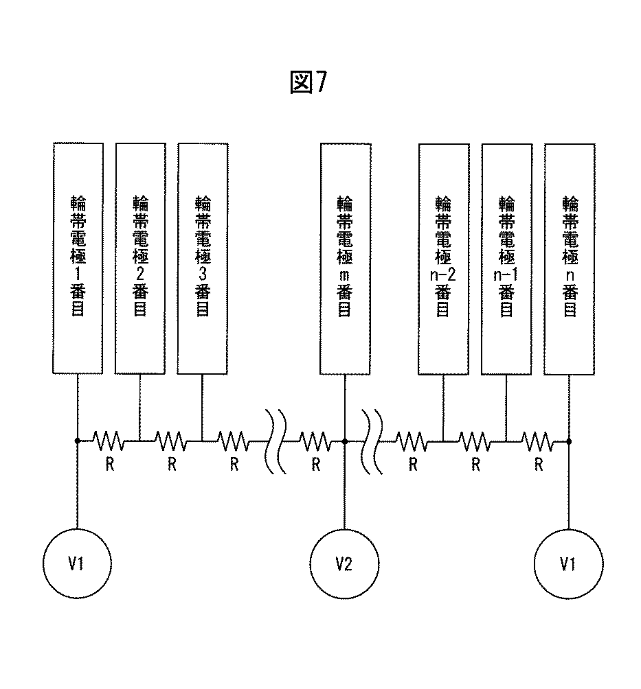
図7は、液晶素子2−1〜2−3がn個の輪帯電極を有する場合の、各輪帯電極と印加される電圧との関係を示す図である。図7では、中心電極を輪帯電極1、最外周の輪帯電極を輪帯電極n、最大電圧を印加する輪帯電極を輪帯電極mとする。この例では、中心電極の輪帯電極1番目と最外周の輪帯電極n番目に同一の電圧V1が、輪帯電極m番目に電圧V2が印加される。
FIG. 7 is a diagram illustrating the relationship between each annular electrode and the applied voltage when the liquid crystal elements 2-1 to 2-3 have n annular electrodes. In FIG. 7, the center electrode is the
ここで、(1)式より、k=0に対応する液晶素子(例えば、液晶素子2−1)の位相変調量のレベル数はMとなり、k≠0に対応する液晶素子(例えば、液晶素子2−2、2−3)の位相変調量のレベル数(M+1)よりも一つ少ない。そこで、k=0に対応する液晶素子における、最大電圧V2と最小電圧V1の差ΔV0=(V2-V1)に対して、k≠0に対応する液晶素子における、最大電圧V2と最小電圧V1の差ΔV1=(V2-V1)は、ΔV1=ΔV0(M+1)/Mとなるように設定される。例えば、図4(A)〜図4(C)に示されるように、k=0に対応する液晶素子2−1のレベル数が6であり、液晶素子2−1において最大位相変調量を与えるレベルと最小位相変調量を与えるレベル間の電圧差がVであれば、レベル数が7となる、液晶素子2−2、2−3において最大位相変調量を与えるレベルと最小位相変調量を与えるレベル間の電圧差は7/6Vとなる。Here, from equation (1), the number of levels of the phase modulation amount of the liquid crystal element (for example, liquid crystal element 2-1) corresponding to k = 0 is M, and the liquid crystal element (for example, liquid crystal element) corresponding to k ≠ 0 One less than the number of levels (M + 1) of the phase modulation amount of 2-2, 2-3). Therefore, in the liquid crystal element corresponding to k = 0, with respect to the difference between the maximum voltage V2 and the minimum voltage V1 ΔV 0 = (V2-V1 ), in the liquid crystal element corresponding to k ≠ 0, the maximum voltage V2 and the minimum voltage V1 The difference ΔV 1 = (V2−V1) is set so as to satisfy ΔV 1 = ΔV 0 (M + 1) / M. For example, as shown in FIGS. 4A to 4C, the number of levels of the liquid crystal element 2-1 corresponding to k = 0 is 6, and the maximum phase modulation amount is given in the liquid crystal element 2-1. If the voltage difference between the level and the level giving the minimum phase modulation amount is V, the level number is 7, and the level giving the maximum phase modulation amount and the minimum phase modulation amount are given in the liquid crystal elements 2-2 and 2-3. The voltage difference between levels is 7 / 6V.
また、各液晶素子の最大位相変調量及び最小位相変調量が、液晶光学デバイス1全体が光束に与える最大位相変調量及び最小位相変調量を、液晶光学デバイス1が有する液晶素子の数で当分した位相変調量となるように、各液晶素子に印加される電圧は決定されればよい。
Further, the maximum phase modulation amount and the minimum phase modulation amount of each liquid crystal element are equivalent to the maximum phase modulation amount and the minimum phase modulation amount given to the light beam by the entire liquid crystal
また、液晶光学デバイス1が光束に与える位相分布は、光軸対称な分布でなくてもよい。例えば、液晶光学デバイス1は、液晶光学デバイス1が配置された光学系全体で生じるコマ収差といった、光軸に対して非対称な波面収差を補正する位相分布を光束に与えられるように、各液晶素子の透明電極13の配置パターンが決定されてもよい。
Further, the phase distribution given to the light flux by the liquid crystal
図8は、N=3、M=7としたときに、(1)式に従って決定された、液晶素子2−1〜2−3の位相変調プロファイルの他の一例を表す図である。また図9は、液晶光学デバイス1全体を透過した光束に与えられる位相変調プロファイルの他の一例を示す図である。図8に示される理想的な位相変調プロファイル800、及び、図9に示される各液晶素子が高速に与える位相変調プロファイルを合成したものに対応する理想的な位相変調プロファイル900は、例えば、液晶光学デバイス1を有する光学系が生じるコマ収差といった非対称な収差を補正するものである。
FIG. 8 is a diagram illustrating another example of the phase modulation profile of the liquid crystal elements 2-1 to 2-3 determined according to the equation (1) when N = 3 and M = 7. FIG. 9 is a diagram showing another example of the phase modulation profile given to the light beam transmitted through the entire liquid crystal
図8及び図9において、横軸は光軸OAに直交する面における位置を表す。なお横軸において光軸OAの位置は0で表される。縦軸は位相変調量を表す。図8の位相変調プロファイル810に示されるように、液晶素子2−1(k=0)が与える位相変調量は、6レベルに等分割される。そして各レベルに対応する液晶層10の部分ごとに部分電極が配置される。一方、位相変調プロファイル820、830に示されるように、液晶素子2−2(k=1)及び液晶素子2−3(k=2)が与える位相変調量は、7レベルに等分割される。この場合も、位相変調量の隣接レベル間の境界の位置、すなわち、隣接する部分電極間の境界の位置が、液晶素子ごとに異なる。そのため、図9の位相変調プロファイル910に示されるように、液晶光学デバイス1を透過する光束に対して与えられる位相変調量は、18レベルに等分割されたものとなる。このように、液晶光学デバイス1全体が光束に与える位相変調プロファイル910と対応する理想的な位相変調プロファイル900の差は、個々の液晶素子が光束に与える位相変調プロファイル810〜830と理想的な位相変調プロファイル800の差よりも小さくなっている。
8 and 9, the horizontal axis represents a position on a plane orthogonal to the optical axis OA. In the horizontal axis, the position of the optical axis OA is represented by 0. The vertical axis represents the phase modulation amount. As shown in the
なお、図8に示されるように、位相変調量の極大点、極小点及び液晶層のアクティブ領域の最外周での位相変調量がそれぞれ異なる場合には、その極大点、極小点及びアクティブ領域の最外周に設けられた部分電極に、引き出し電極を介して、その部分電極が設けられた部分の位相変調量に応じた電圧が制御回路3から供給される。そして、隣接する部分電極間は同一の電気抵抗を持つ電極(抵抗子)によって接続されればよい。
As shown in FIG. 8, when the maximum and minimum points of the phase modulation amount are different from each other and the phase modulation amount at the outermost periphery of the active region of the liquid crystal layer is different, the maximum point, the minimum point, and the active region. A voltage corresponding to the phase modulation amount of the portion where the partial electrode is provided is supplied from the
なお、制御回路3から各液晶素子の輪帯電極に電力を供給するための引き出し電極は、それぞれ、光軸OAと直交する面における同じ位置に設けられてもよい。これにより、液晶光学デバイス1に入射する光束のうち、引き出し電極を透過する部分の割合が小さくなるので、液晶光学デバイス1は、その入射光束のより多くの部分に対して所望の位相分布を与えることができる。
Note that the extraction electrode for supplying power from the
以上に説明してきたように、この液晶光学デバイスは、入射する光束に対する部分電極間の境界の位置が液晶素子ごとに異なるように透明電極のパターンが決定される。そのため、この液晶光学デバイスは、個々の液晶素子の透明電極のパターンの解像度よりも微細な解像度を持つ位相分布を透過する光束に与えることができる。そのため、この液晶光学デバイスは、光束に与える理想的でかつ連続的な位相分布と実際に光束に与えられる離散的な位相分布との誤差を少なくすることができるので、光束に対してより適切な位相分布を与えることができる。さらに、この液晶光学デバイスは、液晶光学デバイス全体として光束に与える位相変調量のレベル数よりも、個々の液晶素子が光束に与える位相変調量のレベル数を少なくできるので、個々の液晶素子が有する部分電極の数も少なくて済む。そのため、この液晶光学デバイスは、部分電極間のギャップ及び引き出し電極の数を抑制できる。 As described above, in this liquid crystal optical device, the pattern of the transparent electrode is determined so that the position of the boundary between the partial electrodes with respect to the incident light beam is different for each liquid crystal element. Therefore, this liquid crystal optical device can give a light flux that transmits a phase distribution having a resolution finer than the resolution of the pattern of the transparent electrode of each liquid crystal element. For this reason, this liquid crystal optical device can reduce an error between an ideal and continuous phase distribution given to the light flux and a discrete phase distribution actually given to the light flux. A phase distribution can be given. Furthermore, since this liquid crystal optical device can reduce the number of levels of the phase modulation amount given to the light beam by each liquid crystal element, compared to the number of levels of the phase modulation amount given to the light beam as a whole of the liquid crystal optical device, each liquid crystal element has The number of partial electrodes can be small. Therefore, this liquid crystal optical device can suppress the gap between the partial electrodes and the number of extraction electrodes.
なお、各液晶素子における、隣接する二つの部分電極間の複数の境界のうちの一部の境界については、各液晶素子を透過する光束に対して同じ位置となっていてもよい。この場合でも、隣接する二つの部分電極間の複数の境界の他の境界については、各液晶素子を透過する光束に対して異なる位置となるため、液晶光学デバイスは、個々の液晶素子の透明電極のパターンの解像度よりも微細な解像度を持つ位相分布を透過する光束に与えることができる。 Note that some of the plurality of boundaries between two adjacent partial electrodes in each liquid crystal element may be at the same position with respect to the light beam transmitted through each liquid crystal element. Even in this case, since the other boundaries of the plurality of boundaries between the two adjacent partial electrodes are in different positions with respect to the light beams transmitted through the respective liquid crystal elements, the liquid crystal optical device is a transparent electrode of each liquid crystal element. The phase distribution having a resolution finer than the resolution of the pattern can be given to the transmitted light beam.
また、変形例によれば、液晶光学デバイスは、任意の方向の偏光面を持つ光束についても所望の位相変調を行えるように、上記の液晶素子の組を二組有し、各組の液晶素子の電極の配置パターン及び液晶の配列方向を互いに直交させてもよい。あるいは、液晶光学デバイスは、補正対象とする収差の種類ごとに、上記の液晶素子の組を有してもよい。 Further, according to the modification, the liquid crystal optical device has two sets of the above liquid crystal elements so that a desired phase modulation can be performed even for a light beam having a polarization plane in an arbitrary direction. The electrode arrangement pattern and the liquid crystal arrangement direction may be orthogonal to each other. Alternatively, the liquid crystal optical device may have a set of the above liquid crystal elements for each type of aberration to be corrected.
さらに他の変形例によれば、隣接する部分電極間の印加電圧の差は異なっていてもよい。すなわち、個々の液晶素子による、位相変調量の隣接レベル間の差はレベルごとに異なっていてもよい。例えば、部分電極が微細になることを避けるために、少なくとも一つの液晶素子において、位相調整量の隣接する二つの極値間の光軸に直交する面に沿った間隔が狭いほど、すなわち、位相調整量が急峻に変化するほど、その間隔に含まれる位相変調量のレベルの数を少なくしてもよい。 According to still another modification, the difference in applied voltage between adjacent partial electrodes may be different. That is, the difference between adjacent levels of the phase modulation amount due to individual liquid crystal elements may be different for each level. For example, in order to prevent the partial electrode from becoming finer, in at least one liquid crystal element, the smaller the interval along the plane perpendicular to the optical axis between two adjacent extreme values of the phase adjustment amount, that is, the phase As the adjustment amount changes sharply, the number of levels of the phase modulation amount included in the interval may be reduced.
図10(A)〜図10(C)は、それぞれ、変形例による、図3に示された位相変調プロファイルに相当する位相変調を光束に与えるための、液晶素子2−1〜2−3の位相変調プロファイルの一例及び対応する輪帯電極パターンを表す図である。図10(A)〜図10(C)の上側において、横軸は光軸OAに直交する面における位置を表す。なお横軸において光軸OAの位置は0で表される。縦軸は位相変調量を表す。図10(A)〜図10(C)の下側には、液晶素子2−1〜2−3に設けられる輪帯電極のパターン1011、1021、1031が表される。図3と同様に、輪帯電極間のギャップは実線で示されている。なお、この変形例でも、N=3として、(1)式に従って輪帯電極パターンが決定されている。
FIGS. 10A to 10C respectively show liquid crystal elements 2-1 to 2-3 for applying phase modulation corresponding to the phase modulation profile shown in FIG. It is a figure showing an example of a phase modulation profile and a corresponding annular zone electrode pattern. 10A to 10C, the horizontal axis represents a position on a plane orthogonal to the optical axis OA. In the horizontal axis, the position of the optical axis OA is represented by 0. The vertical axis represents the phase modulation amount. 10A to 10C show
図10(A)の位相変調プロファイル1010に示されるように、位相変調量が極小値となる光軸の位置0から、位相変調量が極大値となる位置r1までは、図4(A)に示される位相変調プロファイルと同様に、位相変調量は6レベル(すなわち、M=6)に等分割されている。一方、位置r1から、アクティブ領域の最外周となる位置、すなわち、位置r1に隣接する、位相変調量が極小値となる位置r2までは、位相変調量は4レベルに分割されている。特に、位相変調量が急峻になる部分では、隣接レベル間の位相変調量の差が、位置0からr1までの範囲における隣接レベル間の位相変調量の差の2倍になっている。そのため、この変形例では、図3の位相変調プロファイル300に対応する、理想的な位相変調プロファイル1000において、図4(A)に示される輪帯電極パターンが有する輪帯の数よりも少ない、9個の輪帯が設定される。
As shown in the
なお、図7に示されるように、位相変調量が極値となる輪帯電極が制御回路3と接続される例では、このような位相変調プロファイルを実現するために、隣接レベル間の位相変調量差が大きくなるほど、対応する二つの輪帯電極を結ぶ抵抗子の抵抗値が大きくなればよい。図10(A)の例では、液晶素子2−1の輪帯電極のパターン1011において、隣接レベル間の位相変調量の差が、他の部分における、隣接レベル間の位相変調量の差の2倍となる部分に相当する、最外周から2番目の輪帯電極1011aと3番目の輪帯電極1011bとの間に接続される抵抗子、及び、輪帯電極1011bと最外周から4番目の輪帯電極1011cとの間に接続される抵抗子は、他の輪帯電極間に接続される抵抗子の抵抗値と比較して、2倍の抵抗値を持つ。
As shown in FIG. 7, in the example in which the annular electrode whose phase modulation amount is an extreme value is connected to the
同様に、図10(B)、図10(C)の位相変調プロファイル1020、1030に示されるように、光軸の位置0から、位相変調量が極大値となる位置r1までは、液晶素子2−2(k=1)及び液晶素子2−3(k=2)が与える位相変調量は、7レベルに等分割される。一方、位置r1から位置r2までは、位相変調量は、それぞれ、5レベル、4レベルに分割されている。そして位相変調プロファイル1020及び1030においても、位相変調量が急峻になる部分では、隣接レベル間の位相変調量の差が、位置0からr1までの範囲における隣接レベル間の位相変調量の差の2倍になっている。そのため、液晶素子2−2、2−3の輪帯電極パターン1021、1031では、図4(B)及び図4(C)に示される輪帯電極パターンが有する輪帯の数よりも少ない、11個、10個の輪帯が設定される。なお、この変形例においても、隣接する輪帯間の境界の位置が、液晶素子ごとに異なる。
Similarly, as shown in the
図11は、図10(A)〜図10(C)に示される輪帯電極パターンを持つ各液晶素子が光束に与える位相分布のずれを表す図である。また図12は、液晶光学デバイス全体を透過した光束に与えられる位相分布の一例を示す図である。図11及び図12において、横軸は光軸OAに直交する面における位置を表す。なお横軸において光軸OAの位置は0で表される。縦軸は位相変調量を表す。そして図11における曲線1000は、個々の液晶素子が光束に与える理想的な位相変調プロファイルを表し、図10(A)〜図10(C)における位相変調プロファイル1000に対応する。位相変調プロファイル1010〜1030は、それぞれ、液晶素子2−1〜2−3が光束に与える位相変調を表し、図10(A)〜図10(C)における位相変調プロファイル1010〜1030に対応する。また図12において点線で示される位相変調プロファイル1200は、各液晶素子により与えられる位相変調プロファイルを合成して得られる位相変調プロファイル1210に対応する、理想的な位相変調プロファイルを表す。図11に示されるように、液晶素子ごとに、位相変調量の隣接レベル間の境界位置が異なる。そのため、図12の位相変調プロファイル1210に示されるように、液晶光学デバイス1を透過する光束に対して与えられる位相変調量は、30個の輪帯によって18レベルに等分割されたものとなる。したがって、この変形例においても、各液晶素子が有する透明電極パターンの解像度よりも、液晶光学デバイス1を透過する光束に与えられる位相分布の解像度の方が高くなる。またこの変形例では、上記の実施形態と比較して、個々の輪帯の幅のうちの最小となる幅が広くなるので、透明基板上での透明電極パターンの形成が容易となる。
FIG. 11 is a diagram showing a phase distribution shift that each liquid crystal element having the annular electrode pattern shown in FIGS. 10A to 10C gives to the light flux. FIG. 12 is a diagram showing an example of the phase distribution given to the light beam transmitted through the entire liquid crystal optical device. 11 and 12, the horizontal axis represents a position on a plane orthogonal to the optical axis OA. In the horizontal axis, the position of the optical axis OA is represented by 0. The vertical axis represents the phase modulation amount. A
また、位相変調量の隣接レベル間の差を個別に調節する場合には、各液晶素子の各部分電極は、互いに絶縁され、各部分電極は、それぞれ、引き出し電極を介して、制御回路から個別にその部分電極が設けられた部分が光束に与える位相変調量に応じた電圧を受ければよい。 Further, when individually adjusting the difference between adjacent levels of the phase modulation amount, each partial electrode of each liquid crystal element is insulated from each other, and each partial electrode is individually separated from the control circuit via the extraction electrode. It is only necessary to receive a voltage corresponding to the amount of phase modulation given to the light flux by the portion where the partial electrode is provided.
図13は、本発明の一つの実施形態または変形例による液晶光学デバイスを備えたレーザー顕微鏡100の概略構成図を示している。コヒーレント光源であるレーザー光源101から出射したレーザー光束は、コリメート光学系102により平行光に調整され、その平行光は、上記の実施形態または変形例による液晶光学デバイス103を透過した後、対物レンズ104によって試料105上に集光される。試料105により反射または散乱した光束もしくは試料により発生した蛍光等、試料の情報を含んだ光束は、光路を逆にたどり、ビームスプリッター106で反射され、第2の光学系であるコンフォーカル光学系107で再び共焦点ピンホール108上に集光される。そして、共焦点ピンホール108が、試料の焦点位置以外からの光束をカットするので、検出器109でSN比の良好な信号が得られる。なお、レーザー光源101は、放射するレーザーの波長が異なる複数のレーザー光源を有していてもよい。
FIG. 13 is a schematic configuration diagram of a laser microscope 100 including a liquid crystal optical device according to one embodiment or a modification of the present invention. The laser beam emitted from the
ここで、対物レンズ104を含む、レーザー光源1から光束の集光位置までの光学系により発生する波面収差を見積もり、その波面収差をキャンセルするような位相分布を位相変調プロファイルとして液晶光学デバイス103に表示することで、このレーザー顕微鏡100は、結像性能を向上させる。
Here, the wavefront aberration generated by the optical system from the
また、以上説明してきた実施形態では、本発明の液晶光学デバイスをレーザー顕微鏡などの光学系の収差補正に用いる例を示したが、本発明は、これらの実施例に限られるものではない。例えば、本発明の液晶光学デバイスは、光軸対称な屈折率分布レンズとして用いられてもよい。 In the embodiments described above, examples of using the liquid crystal optical device of the present invention for aberration correction of an optical system such as a laser microscope are shown, but the present invention is not limited to these examples. For example, the liquid crystal optical device of the present invention may be used as an optical axis symmetric refractive index distribution lens.
1 液晶光学デバイス
2−1〜2−3 液晶素子
3 制御回路
10 液晶層
11、12 透明基板
13、14 透明電極
13−1〜13−n 輪帯電極(部分電極)
15 液晶分子
16 シール部材
100 レーザー顕微鏡
101 レーザー光源
102 コリメート光学系
103 収差補正デバイス
104 対物レンズ
105 試料
106 ビームスプリッター
107 コンフォーカル光学系
108 共焦点ピンホール
109 検出器DESCRIPTION OF
DESCRIPTION OF
Claims (6)
前記N個の液晶素子のそれぞれは、
所定の方向に配向された液晶分子が封入された液晶層と、
前記液晶層を挟んで対向するように配置された二つの透明電極とを有し、
前記二つの透明電極のうちの少なくとも一方は、複数の部分電極を有し、かつ、前記液晶層を透過する光束に与える、前記光軸から前記光束の最外周の間に位相変調量の極値を持つ位相分布における位相変調量の最大値と最小値の差を所定のレベル数で分割したときの各レベルごとに、当該レベルの位相変調量を前記光束に与える前記液晶層の部分に前記複数の部分電極の少なくとも一つが配置され、かつ、前記複数の部分電極のそれぞれの前記光軸から離れる方向の幅は、当該部分電極に対応する位置での前記光軸から離れる方向に沿った前記位相分布における前記位相変調量の変化が緩やかなほど広くなり、
前記光束に対する、隣接する二つの前記部分電極間の境界の位置が前記液晶素子ごとに異なる箇所を有し、
前記N個の液晶素子のうちの少なくとも一つにおいて、
前記位相変調量の隣接する二つの極値のそれぞれに相当する、前記光軸に直交する面における位置の間隔が小さいほど、当該間隔に含まれる位相変調量のレベルの数が少なくなるように前記複数の部分電極が配置されることを特徴とする液晶光学デバイス。 A liquid crystal optical device having N liquid crystal elements arranged along an optical axis, and N is an integer of 2 or more,
Each of the N liquid crystal elements is
A liquid crystal layer encapsulating liquid crystal molecules aligned in a predetermined direction;
Two transparent electrodes arranged to face each other across the liquid crystal layer,
At least one of the two transparent electrodes has a plurality of partial electrodes, and is given to a light beam transmitted through the liquid crystal layer, and an extreme value of a phase modulation amount between the optical axis and the outermost periphery of the light beam For each level when the difference between the maximum value and the minimum value of the phase modulation amount in the phase distribution having a predetermined number of levels is divided, the plurality of the phase modulation amounts of the level are applied to the portion of the liquid crystal layer that gives the luminous flux. And the width of each of the plurality of partial electrodes in the direction away from the optical axis is the phase along the direction away from the optical axis at a position corresponding to the partial electrode. The slower the change in the phase modulation amount in the distribution, the wider it becomes,
With respect to the light beam, to have a portion where the position of the boundary between two adjacent of said partial electrodes is different for each of the liquid crystal element,
In at least one of the N liquid crystal elements,
The smaller the interval between positions in the plane orthogonal to the optical axis corresponding to each of two adjacent extreme values of the phase modulation amount, the smaller the number of levels of the phase modulation amount included in the interval. A liquid crystal optical device comprising a plurality of partial electrodes .
前記制御回路は、前記位相変調プロファイルにおける位相変調量が極大値となる位置に対応する前記部分電極及び前記位相変調量が極小値となる位置に対応する前記部分電極と、対向する前記透明電極との間に、それぞれ、前記位相変調量が極大値及び極小値となるように電圧を印加する、請求項4に記載の液晶光学デバイス。 For each of the N liquid crystal elements, two adjacent partial electrodes of the plurality of partial electrodes are connected by resistors, respectively.
The control circuit includes the partial electrode corresponding to a position where the phase modulation amount in the phase modulation profile is a maximum value, the partial electrode corresponding to the position where the phase modulation amount is a minimum value, and the transparent electrode facing the partial electrode. 5. The liquid crystal optical device according to claim 4 , wherein a voltage is applied so that the phase modulation amount becomes a maximum value and a minimum value, respectively.
前記制御回路は、前記第1の液晶素子における、前記複数の部分電極のうちの前記位相変調量の最大値に対応する部分電極と対向する前記透明電極との間に印加される電圧と、前記位相変調量の最小値に対応する部分電極と対向する前記透明電極との間に印加される電圧との第1の電圧差に対する、前記他の液晶素子における、前記複数の部分電極のうちの前記位相変調量の最大値に対応する部分電極と対向する前記透明電極との間に印加される電圧と、前記位相変調量の最小値に対応する部分電極と対向する前記透明電極との間に印加される電圧との第2の電圧差の比が、前記第1のレベル数に対する前記第2のレベル数の比と等しくなるように、各液晶素子の各部分電極と対向する前記透明電極との間の電圧を制御する、請求項4または5に記載の液晶光学デバイス。 The predetermined number of levels for the first liquid crystal element of the N liquid crystal elements is a first level number, and the predetermined number of levels for the other liquid crystal elements of the N liquid crystal elements. Is a second level number obtained by adding 1 to the first level number,
The control circuit includes a voltage applied between the transparent electrode facing the partial electrode corresponding to the maximum value of the phase modulation amount among the plurality of partial electrodes in the first liquid crystal element; Of the plurality of partial electrodes in the other liquid crystal element, with respect to a first voltage difference from a voltage applied between the partial electrode corresponding to the minimum value of the phase modulation amount and the transparent electrode facing the partial electrode. Applied between a voltage applied between the partial electrode corresponding to the maximum value of the phase modulation amount and the transparent electrode facing the partial electrode, and between the transparent electrode facing the partial electrode corresponding to the minimum value of the phase modulation amount Of the transparent electrode facing each partial electrode of each liquid crystal element so that the ratio of the second voltage difference to the applied voltage is equal to the ratio of the second level number to the first level number. controlling the voltage between, claim 4 or The liquid crystal optical device according to.
Applications Claiming Priority (3)
| Application Number | Priority Date | Filing Date | Title |
|---|---|---|---|
| JP2013262481 | 2013-12-19 | ||
| JP2013262481 | 2013-12-19 | ||
| PCT/JP2014/080758 WO2015093223A1 (en) | 2013-12-19 | 2014-11-20 | Optical modulation element |
Publications (2)
| Publication Number | Publication Date |
|---|---|
| JPWO2015093223A1 JPWO2015093223A1 (en) | 2017-03-16 |
| JP6478922B2 true JP6478922B2 (en) | 2019-03-06 |
Family
ID=53402578
Family Applications (1)
| Application Number | Title | Priority Date | Filing Date |
|---|---|---|---|
| JP2015553441A Active JP6478922B2 (en) | 2013-12-19 | 2014-11-20 | Light modulation element |
Country Status (5)
| Country | Link |
|---|---|
| US (1) | US20160320677A1 (en) |
| EP (1) | EP3086167A4 (en) |
| JP (1) | JP6478922B2 (en) |
| CN (1) | CN105829958B (en) |
| WO (1) | WO2015093223A1 (en) |
Families Citing this family (5)
| Publication number | Priority date | Publication date | Assignee | Title |
|---|---|---|---|---|
| CN104732168B (en) * | 2015-03-20 | 2017-08-25 | 京东方科技集团股份有限公司 | A kind of display system, control method |
| JP6721698B2 (en) * | 2016-09-26 | 2020-07-15 | 株式会社日立製作所 | Imaging device |
| US11054680B1 (en) * | 2018-08-07 | 2021-07-06 | UltResFP, LLC | Electronically configurable variable aperture and grating for optical and spectral applications |
| CN109782498B (en) * | 2019-01-24 | 2022-02-18 | 南京奥谱依电子科技有限公司 | Liquid crystal micro-mirror for wave-front addressing testing and adjusting, preparation method thereof and optical microscope |
| JP7408422B2 (en) * | 2020-01-30 | 2024-01-05 | 株式会社ジャパンディスプレイ | Light control device and lighting device |
Family Cites Families (10)
| Publication number | Priority date | Publication date | Assignee | Title |
|---|---|---|---|---|
| US4952036A (en) * | 1989-06-07 | 1990-08-28 | In Focus Systems, Inc. | High resolution LCD display system |
| JP4349781B2 (en) * | 2002-09-10 | 2009-10-21 | パイオニア株式会社 | Liquid crystal lens and driving method and apparatus thereof |
| WO2006054803A1 (en) * | 2004-11-22 | 2006-05-26 | Citizen Holdings Co., Ltd. | Liquid crystal optical element and manufacturing method thereof |
| US8885139B2 (en) | 2005-01-21 | 2014-11-11 | Johnson & Johnson Vision Care | Adaptive electro-active lens with variable focal length |
| JP5452834B2 (en) * | 2005-12-28 | 2014-03-26 | エルジー ディスプレイ カンパニー リミテッド | Liquid crystal display |
| US8243251B2 (en) * | 2007-12-06 | 2012-08-14 | Citizen Holdings Co., Ltd. | Liquid crystal fresnel lens |
| US8154804B2 (en) * | 2008-03-25 | 2012-04-10 | E-Vision Smart Optics, Inc. | Electro-optic lenses for correction of higher order aberrations |
| JP5417005B2 (en) * | 2009-03-26 | 2014-02-12 | パナソニック株式会社 | Lighting device |
| CN103309096A (en) * | 2013-06-09 | 2013-09-18 | 京东方科技集团股份有限公司 | Double-layer structural liquid crystal lens and three-dimensional display device |
| KR20150051755A (en) * | 2013-11-05 | 2015-05-13 | 삼성디스플레이 주식회사 | Liquid crystal lens panel and method for manufacturing the same |
-
2014
- 2014-11-20 WO PCT/JP2014/080758 patent/WO2015093223A1/en not_active Ceased
- 2014-11-20 CN CN201480069445.3A patent/CN105829958B/en not_active Expired - Fee Related
- 2014-11-20 US US15/106,094 patent/US20160320677A1/en not_active Abandoned
- 2014-11-20 JP JP2015553441A patent/JP6478922B2/en active Active
- 2014-11-20 EP EP14871172.4A patent/EP3086167A4/en not_active Withdrawn
Also Published As
| Publication number | Publication date |
|---|---|
| EP3086167A1 (en) | 2016-10-26 |
| US20160320677A1 (en) | 2016-11-03 |
| CN105829958B (en) | 2019-08-20 |
| CN105829958A (en) | 2016-08-03 |
| WO2015093223A1 (en) | 2015-06-25 |
| JPWO2015093223A1 (en) | 2017-03-16 |
| EP3086167A4 (en) | 2017-09-13 |
Similar Documents
| Publication | Publication Date | Title |
|---|---|---|
| RU2601227C2 (en) | Multicelled liquid crystal optical instrument with conjugated electric field control | |
| JP6478922B2 (en) | Light modulation element | |
| CN107209437B (en) | Liquid crystal beam steering device with improved area transition and method of making the same | |
| KR100854183B1 (en) | Optical element | |
| US11747708B2 (en) | Polarization-insensitive phase modulator | |
| US9007554B2 (en) | Liquid crystal optical apparatus and image display device | |
| US10168586B2 (en) | Electrically tunable optical phase modulation element | |
| JP6742207B2 (en) | Beam splitting element and microscope device | |
| JP2004101885A (en) | Liquid crystal lens and its driving method, and device | |
| JP2016506541A (en) | Liquid crystal optical device with advanced electric field control capability | |
| JP2012141552A (en) | Liquid crystal cylindrical lens array and display device | |
| CN103365001B (en) | Image display device | |
| US9442302B2 (en) | Liquid crystal lens device and image display device | |
| US10838251B2 (en) | Phase modulation device | |
| JP2018101026A (en) | Liquid crystal lens array | |
| JP2015038535A (en) | Liquid crystal optical element and image display device | |
| US20130215368A1 (en) | Liquid crystal optical apparatus and image display device | |
| US8724063B2 (en) | Liquid crystal optical apparatus, drive device, and image display device | |
| US20190086761A1 (en) | Flat liquid crystal layered fresnel lens device | |
| US11327385B2 (en) | Polarization-insensitive phase modulator | |
| JP2016114899A (en) | Liquid crystal optical device | |
| EP3696598B1 (en) | Phase modulation device | |
| TW201725423A (en) | Liquid crystal beam control device with improved region transition and manufacturing method thereof | |
| JP2017083615A (en) | Liquid crystal optical element | |
| JP2014041381A (en) | Liquid crystal optical element and image display device |
Legal Events
| Date | Code | Title | Description |
|---|---|---|---|
| A621 | Written request for application examination |
Free format text: JAPANESE INTERMEDIATE CODE: A621 Effective date: 20170508 |
|
| A131 | Notification of reasons for refusal |
Free format text: JAPANESE INTERMEDIATE CODE: A131 Effective date: 20180605 |
|
| A521 | Request for written amendment filed |
Free format text: JAPANESE INTERMEDIATE CODE: A523 Effective date: 20180806 |
|
| TRDD | Decision of grant or rejection written | ||
| A01 | Written decision to grant a patent or to grant a registration (utility model) |
Free format text: JAPANESE INTERMEDIATE CODE: A01 Effective date: 20190108 |
|
| A61 | First payment of annual fees (during grant procedure) |
Free format text: JAPANESE INTERMEDIATE CODE: A61 Effective date: 20190205 |
|
| R150 | Certificate of patent or registration of utility model |
Ref document number: 6478922 Country of ref document: JP Free format text: JAPANESE INTERMEDIATE CODE: R150 |
|
| R250 | Receipt of annual fees |
Free format text: JAPANESE INTERMEDIATE CODE: R250 |
|
| R250 | Receipt of annual fees |
Free format text: JAPANESE INTERMEDIATE CODE: R250 |