JP6474640B2 - Current detection resistor - Google Patents
Current detection resistor Download PDFInfo
- Publication number
- JP6474640B2 JP6474640B2 JP2015037759A JP2015037759A JP6474640B2 JP 6474640 B2 JP6474640 B2 JP 6474640B2 JP 2015037759 A JP2015037759 A JP 2015037759A JP 2015037759 A JP2015037759 A JP 2015037759A JP 6474640 B2 JP6474640 B2 JP 6474640B2
- Authority
- JP
- Japan
- Prior art keywords
- resistor
- current
- fusing
- terminal
- terminals
- Prior art date
- Legal status (The legal status is an assumption and is not a legal conclusion. Google has not performed a legal analysis and makes no representation as to the accuracy of the status listed.)
- Active
Links
- 238000001514 detection method Methods 0.000 title claims description 28
- 239000000758 substrate Substances 0.000 claims description 9
- 230000004048 modification Effects 0.000 description 10
- 238000012986 modification Methods 0.000 description 10
- 239000002184 metal Substances 0.000 description 6
- 230000020169 heat generation Effects 0.000 description 5
- 238000004519 manufacturing process Methods 0.000 description 5
- 239000000463 material Substances 0.000 description 5
- 238000002844 melting Methods 0.000 description 4
- 230000008018 melting Effects 0.000 description 4
- 238000000926 separation method Methods 0.000 description 4
- 239000000956 alloy Substances 0.000 description 3
- 229910017566 Cu-Mn Inorganic materials 0.000 description 2
- 229910017871 Cu—Mn Inorganic materials 0.000 description 2
- 229910018487 Ni—Cr Inorganic materials 0.000 description 2
- 206010037660 Pyrexia Diseases 0.000 description 2
- 229910045601 alloy Inorganic materials 0.000 description 2
- 238000005520 cutting process Methods 0.000 description 2
- 238000003466 welding Methods 0.000 description 2
- 230000002159 abnormal effect Effects 0.000 description 1
- 238000004891 communication Methods 0.000 description 1
- 239000012141 concentrate Substances 0.000 description 1
- 230000002500 effect on skin Effects 0.000 description 1
- 238000010894 electron beam technology Methods 0.000 description 1
- 230000017525 heat dissipation Effects 0.000 description 1
- 238000010438 heat treatment Methods 0.000 description 1
- 238000009434 installation Methods 0.000 description 1
- 239000011810 insulating material Substances 0.000 description 1
- 238000005304 joining Methods 0.000 description 1
- 238000000691 measurement method Methods 0.000 description 1
- 239000007769 metal material Substances 0.000 description 1
- 230000002093 peripheral effect Effects 0.000 description 1
- 238000004080 punching Methods 0.000 description 1
- 230000005855 radiation Effects 0.000 description 1
- 229910000679 solder Inorganic materials 0.000 description 1
- 238000009423 ventilation Methods 0.000 description 1
Images


Landscapes
- Fuses (AREA)
Description
本発明は、抵抗体に流れる電流を検出する電流検出用抵抗器に関する。 The present invention relates to a current detection resistor that detects a current flowing through a resistor.
各種電気機器、例えば、電気自動車やその充電施設等において、電流検出が行われている。電流検出においては、シャント式の電流測定法が用いられ、一例として、金属板の抵抗体および電極端子を備えた電流検出用抵抗器が用いられている。 Current detection is performed in various electric devices such as electric vehicles and charging facilities thereof. In the current detection, a shunt-type current measurement method is used. As an example, a current detection resistor including a metal plate resistor and an electrode terminal is used.
そして、上記電気機器においては、故障時などに過電流が流れることによる安全性確保の対応が必要であり、過電流に対する対策、すなわち、過電流が流れることによる機器損傷の被害拡大の防止の対策を施すことが必要となっている。 And in the above electrical equipment, it is necessary to take measures to ensure safety due to overcurrent flowing at the time of failure, etc., and measures against overcurrent, that is, measures to prevent the expansion of damage to equipment due to overcurrent flowing. It is necessary to apply.
過電流による機器損傷防止の対策として、例えば電流ヒューズを搭載し、過電流を遮断して機器を保護するのが一般的である。しかしながら、一方で機器の小型化の要求もあり、電流遮断機能を備えた電流ヒューズ等を搭載するスペースの確保が困難な場合もある。 As a measure for preventing damage to equipment due to overcurrent, for example, a current fuse is generally mounted, and overcurrent is interrupted to protect the equipment. However, on the other hand, there is a demand for miniaturization of equipment, and it may be difficult to secure a space for mounting a current fuse or the like having a current interruption function.
ところで、下記特許文献1が知られている。この文献には、電流検出用抵抗器31の金属抵抗体からなる脚部35と梁部34の境界付近に開口32を形成した構造が記載されている(図1参照)。そして、開口32を設けることで、全体の形状を大きくすることなく、且つ強度を低下させることなく所望の抵抗値が得られ、しかも、金属抵抗体で発生したジュール熱がスムーズにプリント基板に流れ、且つ通風を良好にして、温度があまり上昇しないことが記載されている。従って、「電流遮断機能を備える」ことについては一切記載がない。
Incidentally, the following Patent Document 1 is known. This document describes a structure in which an
本発明は、上述の事情に基づいてなされたもので、電流遮断機能を備えた電流検出用抵抗器を提供することを目的とする。 The present invention has been made based on the above-described circumstances, and an object thereof is to provide a current detection resistor having a current interrupt function.
本発明の電流検出用抵抗器は、抵抗体と、該抵抗体に接続された一対の端子と、少なくとも一方の端子の一部に、狭い電流路とした溶断部を備えた抵抗器であって、前記溶断部は、前記電流路を狭くする狭小部を備え、所定の溶断電流が印加されたときに、前記溶断部が溶断するようにした、ことを特徴とする。
A current detection resistor according to the present invention is a resistor including a resistor, a pair of terminals connected to the resistor, and a fusing part as a narrow current path in a part of at least one of the terminals. The fusing part includes a narrow part that narrows the current path, and the fusing part is blown when a predetermined fusing current is applied.
本発明によれば、抵抗器の端子に電流遮断機能を具備したので、過電流の遮断が可能な電流検出用抵抗器を、通常の電流検出用抵抗器と略同サイズで形成できる。Cu等の端子材は高導電性で、高熱伝導性で且つ正の高いTCRを有する。抵抗体に隣接した端子部分に狭い電流路である溶断部を形成したことで、大電流によりまず抵抗体のジュール熱で溶断部が加熱され、高い正のTCRにより溶断部自体の抵抗が増加して発熱が加速することで、溶断に至ると考えられる。これにより、コンパクトな構造で電流遮断機能を形成できる。 According to the present invention, since the resistor terminal is provided with a current interruption function, a current detection resistor capable of interrupting overcurrent can be formed in substantially the same size as a normal current detection resistor. A terminal material such as Cu has high conductivity, high thermal conductivity, and high positive TCR. By forming a fusing part which is a narrow current path in the terminal part adjacent to the resistor, the fusing part is first heated by the Joule heat of the resistor due to a large current, and the resistance of the fusing part itself is increased by a high positive TCR. It is thought that the fever accelerates and leads to fusing. Thereby, a current interruption function can be formed with a compact structure.
以下、本発明の実施形態について、図1乃至図10を参照して説明する。なお、各図中、同一または相当する部材または要素には、同一の符号を付して説明する。 Hereinafter, embodiments of the present invention will be described with reference to FIGS. 1 to 10. In addition, in each figure, the same code | symbol is attached | subjected and demonstrated to the same or equivalent member or element.
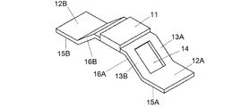
図1は本発明の実施例1の電流検出用抵抗器を示す。この抵抗器は、抵抗体11と、抵抗体に接続された一対の端子12A、12Bと、を備えた抵抗器である。抵抗体11には、Cu−Mn系、Ni−Cr系などの低抵抗率で且つ低TCR(抵抗温度係数)の抵抗合金材が用いられる。端子12A,12Bには、Cu等の高導電性で、高熱伝導性で、且つ正の高いTCRを有する金属材が用いられる。抵抗体11は一部を削る等により抵抗値調整をしてもよい。
FIG. 1 shows a current detection resistor according to a first embodiment of the present invention. This resistor is a resistor provided with a
この抵抗器においては、一方の端子12Aの一部に、狭い電流路とした溶断部13A,13Bを形成し、所定の溶断電流が印加されたときに、該溶断部が溶断するようにしている。すなわち、電流検出用抵抗器の端子部分に所定の溶断電流で溶断し、電流を遮断するヒューズ機能を持たせている。
In this resistor,
この実施例1では、端子12Aに開口部14が形成されている。この開口部14によって、溶断部13A,13Bが開口部14の両側に2ヶ所形成されている。溶断部13A,13Bの幅、厚み、長さは略同一として、電気抵抗が略同じになるようにする。これにより、溶断部13A,13Bへの電流負荷がなるべく偏らず、均等になる。そして、溶断部の幅、厚み、長さ等により溶断電流が決まってくる。
In the first embodiment, an
図2は実施例1の抵抗器が実装された状態を示す。一対の端子12A,12Bは、抵抗器が実装される実装基板20上の実装ランド21A,21Bに接する実装部15A,15Bを備え、該実装部がハンダ等により実装ランド21A,21Bに接合される。そして、抵抗体11および溶断部13A,13Bが実装基板20から離隔した構造となるように、端子12A,12Bは離隔部16A,16Bを備える。溶断部13A、13Bは、実装部15Aから抵抗体11に及んで構成されている。
FIG. 2 shows a state where the resistor of the first embodiment is mounted. The pair of
これにより、抵抗体11および溶断部13A,13Bは浮いた状態となり、その下に、電圧検出配線パターン22A,22Bが配置され、該電圧検出配線パターンは実装ランド21A,21Bに接続されている。従って、抵抗体11を流れる電流によって生じた電圧は離隔部16A,16B、実装部15A,15Bおよび電圧検出パターン22A,22Bを介して図示しない電圧検出装置により取り出される。
As a result, the
溶断部13A,13Bにより形成される電流路は、端子12Aの実装部15Aや端子12Bの実装部15Bよりも幅が狭く、また抵抗体11よりも幅が狭く、電流が集中する構造である。ただし、当然のことながら、溶断部の電気抵抗値は抵抗体の電気抵抗値よりも低い。
The current path formed by the
抵抗体11は、TCRが、端子(Cu)12A,12BのTCRよりもはるかに低く、端子(Cu)部分は高い正のTCRを有する。そして、電流検出用抵抗器は、抵抗体11と端子12A,12Bとが直列に接続されている。すなわち、同じ電流に対して、二乗に比例して温度上昇する部分(抵抗体部分)と、二乗以上に比例して温度上昇する部分(端子部分)を直列に接続した構成である。
The
また、抵抗体11と溶断部13A,13Bは隣接しており、該抵抗体と該溶断部は熱的に良好に接続された構造である。このため、抵抗器が通常使用される電流領域、即ち抵抗体それ自体の発熱が支配的な電流領域では、温度上昇はほぼ電流の二乗に比例するが、電流がある閾値を超えると、TCRが高い端子部分(溶断部13A,13B)の温度が上昇して支配的となり、これに抵抗体11の発熱が加わることで、端子(溶断部13A,13B)部分の温度上昇が更に加速する。これにより、該溶断部の発熱が促進され、溶断に至る。したがって、コンパクトな構造で電流遮断機能を形成でき、例えばCu線のみからなる通常の電流ヒューズとは異なる電流遮断特性が得られる。
Further, the
また、突入電流(溶断電流)の立ち上がりが大きく、大電流である場合は、表皮効果によって端子(溶断部13A,13B)の外周部への電流密度の集中が期待出来る。このため、溶断部13A,13Bのように、端子12Aの外側に抵抗の大きな溶断部を配する構造にすれば、該溶断部が溶断し易くなる。一方の溶断部が溶断すれば、他方の溶断部へ負荷が集中して溶断するので、電流が遮断される。
In addition, when the inrush current (melting current) rises greatly and is a large current, the concentration of current density on the outer peripheral portion of the terminal (melting
溶断電流(異常電流)印加時に、溶断部13A,13Bが溶断温度に速やかに達する為に、該溶断部(及び抵抗体11)からの外因性の放熱を極力抑える方が良い。このため、該溶断部と、発熱体である該抵抗体が実装基板等への外因性の放熱体に接触する事を避けることが望ましい。このため、本実施例においては、端子12A,12Bをフォーミングして離隔部16A,16Bを形成することによって、該溶断部と該抵抗体を実装基板20から浮かせる構造としている。
When the fusing current (abnormal current) is applied, in order for the
図3A−3Dは実施例1の抵抗器の製造工程例を示す。まず、図3Aに示すように、抵抗体に用いるCu−Mn系或いはNi−Cr系等の抵抗合金板材31と、端子に用いるCu等の金属板材32を準備する。そして、抵抗合金板材31の両側に端子用の金属板材32を接合する。接合はレーザー溶接や電子ビーム溶接等により形成される。
3A to 3D show an example of a manufacturing process of the resistor of the first embodiment. First, as shown in FIG. 3A, a Cu-Mn-based or Ni-Cr-based
これにより、図3Bに示すように、抵抗体11の両側に端子12A,12Bを備えた本件発明の抵抗器の原型となる構造が得られる。そして、図3Cに示すように、端子12Aの一部をパンチング等により打ち抜いて、貫通した開口部14を形成する。これにより、開口部14の両側に溶断部13A,13Bが形成される。
Thereby, as shown to FIG. 3B, the structure used as the prototype of the resistor of this invention provided with terminal 12A, 12B on the both sides of the
次に、端子12A,12Bを折り曲げ加工し、抵抗体11および溶断部13A,13Bを実装面から離隔した構造にする離隔部16A、16Bを形成する。これにより、図3Dに示すように、実装ランド21A,21Bに接合する実装部15A,15Bを底面に備え、端子12A,12Bを折り曲げ加工して、抵抗体11および溶断部13A,13Bが実装面から浮き上がり離隔した構造の抵抗器が完成する。
Next, the
図4は実施例1の抵抗器の変形例を示す。この変形例においては、溶断部13A,13Bに、さらに電流路を狭くした狭小部Sを形成するための切り込み17A,17Bを備えている。これにより、局所的に電流路の抵抗値を上げることができるので、溶断するポイントを予め特定することができる。
FIG. 4 shows a modification of the resistor of the first embodiment. In this modification, the fusing
すなわち、切り込み17A,17Bを設けることで、その部分で電流路の抵抗値が上昇し、その部分で発熱量が多くなることから、その部分で溶断する。切り込み17A,17Bは、抵抗体11の発熱を良好に伝導させるため、抵抗体11に近い位置にすることが望ましい。そして、切り込み17A,17Bの大小および設置位置で溶断電流の大きさを調整可能である。
That is, by providing the
図5Aは実施例2の抵抗器を示す。この実施例2は、溶断部13Cを一ヶ所に構成した例である。この例でも、溶断部13Cは、実装部15Aから抵抗体11に及んで構成されている。そして、一方の端子12Aの一部に、他方の端子12Bおよび抵抗体11よりも狭い電流路とした溶断部13Cを形成し、所定の溶断電流が印加されたときに、溶断部13Cが溶断する。
FIG. 5A shows the resistor of the second embodiment. This Example 2 is an example in which the
図5Bは実施例2の変形例を示す。この変形例においても、溶断部13Cに、さらに電流路を狭くした狭小部Sを形成するための切り込み17A,17Bを備えている。これにより、その部分で電流路の抵抗値が上昇し、その部分で発熱量が多くなることから、その部分で溶断する。なお、切り込み17A,17Bはどちらか一ヶ所でもよい。
FIG. 5B shows a modification of the second embodiment. Also in this modification, the fusing
図6は実施例3の抵抗器を示す。低抵抗値の電流検出用抵抗器においては、端子の抵抗成分が抵抗体の抵抗値に対して無視できない場合、二端子構造では端子の抵抗成分による誤差電圧が検出電圧に影響を及ぼすという問題がある。この問題は下記実施例3−5で述べる電流端子と電圧端子を分離した四端子構造で解消可能である。 FIG. 6 shows a resistor according to the third embodiment. In the case of a low-resistance current detection resistor, when the resistance component of the terminal cannot be ignored relative to the resistance value of the resistor, the error voltage due to the resistance component of the terminal affects the detection voltage in the two-terminal structure. is there. This problem can be solved by a four-terminal structure in which a current terminal and a voltage terminal described in Example 3-5 below are separated.
実施例3の抵抗器は、実施例1の抵抗器を四端子構造としたものであり、電流端子12C,12Dに併設して電圧端子12c,12dを構成した例である。実施例1の抵抗器においては、図2に示すように、端子12Aに溶断部13A,13Bを形成したことにより、端子12Aの抵抗成分により電圧検出パターン22A,22Bにより検出される電圧が、抵抗体11の両端に形成される電圧よりも高くなり、検出誤差が生じる。
The resistor of the third embodiment is an example in which the resistor of the first embodiment has a four-terminal structure, and the
実施例3の抵抗器によれば、電流端子12Cと電圧端子12c,電流端子12Dと電圧端子12dに、端子を分離しているので、電圧端子12c,12dは抵抗体11の直近での電圧検出が可能となり、電流端子12Cの溶断部13A,13Bにおける抵抗分増大の影響を受けることなく、高精度の電圧検出が可能となる。
According to the resistor of the third embodiment, since the terminals are separated into the
図7Aと図7Bは実施例4の抵抗器を示す。この抵抗器も実施例3の抵抗器と同様に四端子構造の電流検出用抵抗器である。しかしながら、実施例3の抵抗器が電流端子と電圧端子を併設しているのに対し、実施例4では電圧端子を開口部の抵抗体側中央に配置し、その両側に電流端子を配置した構成である点で相違する。 7A and 7B show the resistor of Example 4. FIG. Similar to the resistor of the third embodiment, this resistor is also a four-terminal current detection resistor. However, while the resistor of Example 3 has both a current terminal and a voltage terminal, in Example 4, the voltage terminal is arranged in the center of the resistor side of the opening, and the current terminals are arranged on both sides thereof. There are some differences.
電流端子として機能する端子12Eから開口部14Aを打ち抜き形成する際に、端子材の一部を残しておき、曲げ加工して電圧端子12eを構成した例である。電流端子として機能する端子12F側も、端子12Eと同様に、開口部14Bを形成して、打ち抜いた端子材を曲げ加工して電圧端子12fを形成する。
In this example, when the
このとき、開口部14Bは開口部14Aよりも細く形成して、開口部14Bにおける溶断部に相当する部位(連通部)を、溶断部13A,13Bよりも低い抵抗値となるようにしている。従って、溶断は電流路が狭い溶断部13A,13Bにて生じる。なお、開口部14Bを形成したことにより、抵抗体11の発熱が端子12F側に放熱されることが抑制されるため、溶断部13A,13Bに対して抵抗体11の熱をより伝え易くすることができる。
At this time, the
図8は実施例5の抵抗器を示す。この抵抗器も実施例3と4の抵抗器と同様に四端子構造の電流検出用抵抗器である。しかしながら、実施例5では電圧端子12g,12hを抵抗器の側部に引き出す構成を採用している点で、実施例3と4の抵抗器と相違する。
FIG. 8 shows the resistor of the fifth embodiment. Similar to the resistors of the third and fourth embodiments, this resistor is also a four-terminal structure current detection resistor. However, the fifth embodiment is different from the resistors of the third and fourth embodiments in that a configuration is adopted in which the
係る構成を採用することで、電圧端子12g,12hが抵抗体11の接合面で、抵抗体11の両端に生じる電圧を直接検出できるという利点が生じる。そして、電流端子12Hに開口や電圧端子のスペースを設ける必要が無く、電流端子としてその全幅を利用できるという利点が生じる。
By adopting such a configuration, there is an advantage that the
図9Aと図9Bは実施例1の他の変形例を示す。この抵抗器は両方の端子12A,12Bにそれぞれ開口部14A,14Bを形成し、それぞれの両側を溶断部13A,13Bとしたものである。開口部14A,14Bを両方の端子に対称に形成することで、実装時の方向性がなくなり、また、抵抗体11の基板20への放熱が抑制されるため、溶断部13A,13Bを高温にするのに好適である。この構造に加えて、図6〜図8に示すように、電圧検出端子を設けた構造にしてもよい。
9A and 9B show another modification of the first embodiment. In this resistor,
図10は抵抗器を実装した状態(図2)の変形例を示す。本発明の抵抗器を基板に実装した場合、溶断時に溶けた金属が飛散し、基板の実装ランド21A,21B間を導通させることが考えられる。それを防ぐために、絶縁材23で実装ランド21A,21B間を絶縁した構造である。これにより、溶断部は溶断したがなお過電流が流れ続ける事態を防止できる。
FIG. 10 shows a modification of the state in which the resistor is mounted (FIG. 2). When the resistor of the present invention is mounted on a substrate, it is conceivable that the metal melted at the time of fusing scatters and makes the mounting
これまで本発明の一実施形態について説明したが、本発明は上述の実施形態に限定されず、その技術的思想の範囲内において種々異なる形態にて実施されてよいことは言うまでもない。 Although one embodiment of the present invention has been described so far, it is needless to say that the present invention is not limited to the above-described embodiment, and may be implemented in various forms within the scope of the technical idea.
本発明は、電流遮断機能が要求される回路で使用される電流検出用抵抗器に好適に利用可能である。 The present invention can be suitably used for a current detection resistor used in a circuit that requires a current interrupt function.
Claims (4)
前記溶断部は、前記電流路を狭くする狭小部を備え、
所定の溶断電流が印加されたときに、前記溶断部が溶断するようにした、電流検出用抵抗器。 A resistor, a pair of terminals connected to the resistor, and a resistor having a fusing part as a narrow current path in a part of at least one terminal ,
The fusing part includes a narrow part that narrows the current path ,
A current detection resistor in which the fusing part is blown when a predetermined fusing current is applied.
Priority Applications (1)
| Application Number | Priority Date | Filing Date | Title |
|---|---|---|---|
| JP2015037759A JP6474640B2 (en) | 2015-02-27 | 2015-02-27 | Current detection resistor |
Applications Claiming Priority (1)
| Application Number | Priority Date | Filing Date | Title |
|---|---|---|---|
| JP2015037759A JP6474640B2 (en) | 2015-02-27 | 2015-02-27 | Current detection resistor |
Publications (2)
| Publication Number | Publication Date |
|---|---|
| JP2016162522A JP2016162522A (en) | 2016-09-05 |
| JP6474640B2 true JP6474640B2 (en) | 2019-02-27 |
Family
ID=56847273
Family Applications (1)
| Application Number | Title | Priority Date | Filing Date |
|---|---|---|---|
| JP2015037759A Active JP6474640B2 (en) | 2015-02-27 | 2015-02-27 | Current detection resistor |
Country Status (1)
| Country | Link |
|---|---|
| JP (1) | JP6474640B2 (en) |
Families Citing this family (4)
| Publication number | Priority date | Publication date | Assignee | Title |
|---|---|---|---|---|
| JP6851070B2 (en) * | 2016-12-13 | 2021-03-31 | 株式会社日之出電機製作所 | Fuse with shunt resistor |
| JP6783389B2 (en) * | 2017-05-31 | 2020-11-11 | 三菱電機株式会社 | Current blocking element and ozone generator |
| KR101884680B1 (en) * | 2017-08-28 | 2018-08-02 | 인텍전기전자 주식회사 | Dc circuit breaker comprising shunt and method for manufacturing shunt of dc circuit breaker |
| WO2024224466A1 (en) * | 2023-04-25 | 2024-10-31 | 三菱電機株式会社 | Printed circuit board and power conversion device |
Family Cites Families (4)
| Publication number | Priority date | Publication date | Assignee | Title |
|---|---|---|---|---|
| JPS5127050U (en) * | 1974-08-20 | 1976-02-27 | ||
| JP2542570Y2 (en) * | 1989-10-18 | 1997-07-30 | ローム 株式会社 | Chip type resistor |
| JP2012119507A (en) * | 2010-12-01 | 2012-06-21 | Fujitsu Ten Ltd | Shunt resistor, electronic controller, and mounting method |
| JP6051947B2 (en) * | 2013-02-28 | 2016-12-27 | 株式会社デンソー | Electronic component and electronic control device |
-
2015
- 2015-02-27 JP JP2015037759A patent/JP6474640B2/en active Active
Also Published As
| Publication number | Publication date |
|---|---|
| JP2016162522A (en) | 2016-09-05 |
Similar Documents
| Publication | Publication Date | Title |
|---|---|---|
| JP6437262B2 (en) | Mounting body manufacturing method, thermal fuse element mounting method, and thermal fuse element | |
| JP6474640B2 (en) | Current detection resistor | |
| JP6580504B2 (en) | Protective element | |
| JP2011034755A5 (en) | ||
| JP4663760B2 (en) | Secondary battery protection circuit | |
| JP2017010859A (en) | Flexible printed wiring board and manufacturing method of flexible printed wiring board | |
| US20170162302A1 (en) | Current detection resistor | |
| KR102481793B1 (en) | Thermal Fuse and Printed Circuit Board with Thermal Fuse | |
| US8937525B2 (en) | Surface mountable over-current protection device | |
| TW201805984A (en) | Protection element | |
| JP7433811B2 (en) | Fuse elements, fuse elements and protection elements | |
| JP2006190981A (en) | Ptc circuit protective device having parallel effective resistance regions | |
| CN110957188A (en) | Disconnecting element and disconnecting element circuit | |
| KR20150029023A (en) | Fuse | |
| KR101529829B1 (en) | The complex protection device of blocking the abnormal state of current and voltage | |
| JP6569693B2 (en) | Electronic circuit and overheat detection method | |
| US10895609B2 (en) | Circuit protection device with PTC element and secondary fuse | |
| JP6102266B2 (en) | fuse | |
| JP7154090B2 (en) | protective element | |
| JP6171500B2 (en) | fuse | |
| JP2002203701A (en) | Resistor unit | |
| JP5494165B2 (en) | Overcurrent detection composite element and overcurrent interruption device provided with overcurrent detection composite element | |
| TWI547967B (en) | Complex protection device | |
| EP3389077B1 (en) | Printed circuit fuse and method for use of the same | |
| JPH11339615A (en) | Substrate type resistor thermal fuse |
Legal Events
| Date | Code | Title | Description |
|---|---|---|---|
| A621 | Written request for application examination |
Free format text: JAPANESE INTERMEDIATE CODE: A621 Effective date: 20180130 |
|
| A977 | Report on retrieval |
Free format text: JAPANESE INTERMEDIATE CODE: A971007 Effective date: 20181026 |
|
| A131 | Notification of reasons for refusal |
Free format text: JAPANESE INTERMEDIATE CODE: A131 Effective date: 20181106 |
|
| A521 | Request for written amendment filed |
Free format text: JAPANESE INTERMEDIATE CODE: A523 Effective date: 20181212 |
|
| TRDD | Decision of grant or rejection written | ||
| A01 | Written decision to grant a patent or to grant a registration (utility model) |
Free format text: JAPANESE INTERMEDIATE CODE: A01 Effective date: 20190108 |
|
| A61 | First payment of annual fees (during grant procedure) |
Free format text: JAPANESE INTERMEDIATE CODE: A61 Effective date: 20190130 |
|
| R150 | Certificate of patent or registration of utility model |
Ref document number: 6474640 Country of ref document: JP Free format text: JAPANESE INTERMEDIATE CODE: R150 |
|
| R250 | Receipt of annual fees |
Free format text: JAPANESE INTERMEDIATE CODE: R250 |
|
| R250 | Receipt of annual fees |
Free format text: JAPANESE INTERMEDIATE CODE: R250 |
|
| R250 | Receipt of annual fees |
Free format text: JAPANESE INTERMEDIATE CODE: R250 |
|
| R250 | Receipt of annual fees |
Free format text: JAPANESE INTERMEDIATE CODE: R250 |