JP6396177B2 - Failure detection device, air conditioner including the same, failure detection method and program - Google Patents
Failure detection device, air conditioner including the same, failure detection method and program Download PDFInfo
- Publication number
- JP6396177B2 JP6396177B2 JP2014225279A JP2014225279A JP6396177B2 JP 6396177 B2 JP6396177 B2 JP 6396177B2 JP 2014225279 A JP2014225279 A JP 2014225279A JP 2014225279 A JP2014225279 A JP 2014225279A JP 6396177 B2 JP6396177 B2 JP 6396177B2
- Authority
- JP
- Japan
- Prior art keywords
- semiconductor element
- inverter circuit
- failure
- predetermined period
- circuit
- Prior art date
- Legal status (The legal status is an assumption and is not a legal conclusion. Google has not performed a legal analysis and makes no representation as to the accuracy of the status listed.)
- Expired - Fee Related
Links
Images


Landscapes
- Inverter Devices (AREA)
Description
本発明は、故障検出装置、それを備えた空気調和装置、及び故障検出方法並びにプログラムに関するものである。 The present invention relates to a failure detection device, an air conditioner including the failure detection device, a failure detection method, and a program.
例えば、インバータエアコンに用いられる圧縮機は、インバータを構成する上下対の3相分の6個の半導体素子を順次オンオフ制御させることで生成される交流電流で駆動される圧縮機モータにより、駆動されている。
ところで、圧縮機が起動不良である場合、半導体素子または圧縮機に不良が生じていることが考えられるが、どちらの不良であるか判断が付けられない場合がある。そのため、従来は、圧縮機を駆動する圧縮機モータに電力供給するインバータの出力端に、半導体素子の不良の有無をテストするためのチェッカーを接続し、半導体素子に不良が生じているか否かを判断していた。
下記特許文献1では、インバータを構成するインバータブリッジ素子のオンオフを切り替えることにより、短絡電流により検出される素子破壊と、通常V/F((Voltage/Frequency)モードにより交流電動機を駆動して検出される過負荷とを区別して表示することが記載されている。
For example, a compressor used in an inverter air conditioner is driven by a compressor motor driven by an alternating current generated by sequentially turning on and off six semiconductor elements for three phases of upper and lower pairs constituting the inverter. ing.
By the way, when the compressor is defective in starting, it is conceivable that a defect has occurred in the semiconductor element or the compressor, but it may not be possible to determine which one is defective. Therefore, conventionally, a checker for testing whether or not a semiconductor element is defective is connected to an output terminal of an inverter that supplies power to a compressor motor that drives the compressor, and whether or not the semiconductor element is defective is determined. I was judging.
In the following Patent Document 1, switching between ON and OFF of an inverter bridge element that constitutes an inverter is detected by driving an AC motor in a normal V / F ((Voltage / Frequency) mode and element breakdown detected by a short-circuit current. It is described that the overload is distinguished and displayed.
しかしながら、従来のようにチェッカーを用いる場合には、インバータからの出力端にチェッカーを接続する配備作業や、チェッカーのメンテナンス作業が必要となり、コストがかかるという問題があった。また、素子に生じる故障は、短絡故障に限られず開放故障も含まれるが、上記特許文献1の方法では、素子に開放故障が生じている場合には、検出できず、インバータの不具合を正確に検出できないという問題があった。 However, when a checker is used as in the prior art, there is a problem that a deployment work for connecting the checker to the output terminal from the inverter and a maintenance work for the checker are required, which increases costs. In addition, the failure occurring in the element is not limited to a short-circuit failure, and includes an open failure. However, in the method of Patent Document 1, when an open failure occurs in the element, it cannot be detected, and the failure of the inverter is accurately detected. There was a problem that it could not be detected.
本発明は、このような事情に鑑みてなされたものであって、簡便に、かつ、安価にインバータの不具合を正確に検出することのできる故障検出装置、それを備えた空気調和装置、及び故障検出方法並びにプログラムを提供することを目的とする。 The present invention has been made in view of such circumstances, a failure detection device capable of accurately detecting a failure of an inverter simply and inexpensively, an air conditioner including the failure detection device, and a failure An object is to provide a detection method and a program.
上記課題を解決するために、本発明は以下の手段を採用する。
本発明の参考例は、直流電力を交流電力に変換してモータに電力供給するインバータ回路の故障検出装置であって、前記モータと前記インバータ回路とが未接続状態とされ、前記インバータ回路は、前記直流電力が供給される正負の電源線と接続され、上アーム回路を構成する第1半導体素子と下アーム回路を構成する第2半導体素子とが直列接続された素子対を複数備えており、各前記第1半導体素子及び各前記第2半導体素子のオンオフ状態を切り替える駆動手段と、前記インバータ回路に流れる電流値を検出する電流検出手段と、各前記素子対において、前記第1半導体素子及び前記第2半導体素子が、同時に第1所定期間オン状態にされる第1制御、及びどちらか一方が前記第1所定期間オン状態にされる第2制御によって検出される前記電流値に基づいて、不具合の有無を判定する不具合判定手段とを具備する故障検出装置を提供する。
In order to solve the above problems, the present invention employs the following means.
A reference example of the present invention is a failure detection device for an inverter circuit that converts DC power into AC power and supplies power to the motor, wherein the motor and the inverter circuit are in an unconnected state, and the inverter circuit is A plurality of element pairs connected in series to a first semiconductor element constituting an upper arm circuit and a second semiconductor element constituting a lower arm circuit, connected to positive and negative power supply lines to which the DC power is supplied; In each of the element pairs, the first semiconductor element and the drive means for switching the on / off state of each of the first semiconductor elements and the second semiconductor elements, current detection means for detecting a current value flowing through the inverter circuit, and Detected by the first control in which the second semiconductor element is simultaneously turned on for the first predetermined period and the second control in which one of the second semiconductor elements is turned on for the first predetermined period. Based on the current value, to provide a failure detection device comprising a fault judging means for judging the presence or absence of a defect.
本発明の参考例の構成によれば、上アーム回路を構成する第1半導体素子と下アーム回路を構成する第2半導体素子とが直列に接続された素子対が複数備えられ、正負の電源線から供給された直流電力を交流電力に変換してモータに電力供給するインバータ回路の故障検出装置は、各素子対において、モータはインバータ回路と未接続状態とされており、第1半導体素子及び第2半導体素子を同時に第1所定期間オン状態にすると、不具合がなければ、第1半導体素子と第2半導体素子とを通じて電流が流れるので、インバータ回路には電流が流れることが推定されるが、所望の電流値が検出されなければ不具合(例えば、開放故障または駆動手段の故障)が生じていると判定される。また、各素子対において、第1半導体素子または第2半導体素子のどちらか一方を第1所定期間オン状態にすると、不具合がなければ、モータはインバータ回路と未接続状態とされており、一方はオフ状態にされているのでインバータ回路に電流が流れないことが推定されるが、電流が検出されれば不具合(例えば、短絡故障または駆動手段の故障)が生じていると判定される。 According to the configuration of the reference example of the present invention , there are provided a plurality of element pairs in which a first semiconductor element constituting the upper arm circuit and a second semiconductor element constituting the lower arm circuit are connected in series, and positive and negative power supply lines In the inverter circuit failure detection device that converts the DC power supplied from the AC power into the AC power and supplies the motor with power, the motor is not connected to the inverter circuit in each element pair. If the two semiconductor elements are turned on for the first predetermined period at the same time, if there is no problem, current flows through the first semiconductor element and the second semiconductor element. If no current value is detected, it is determined that a malfunction (for example, an open failure or a drive means failure) has occurred. Further, in each element pair, when one of the first semiconductor element and the second semiconductor element is turned on for the first predetermined period, if there is no problem, the motor is not connected to the inverter circuit. It is estimated that no current flows through the inverter circuit because it is in the off state, but if a current is detected, it is determined that a malfunction (for example, a short circuit failure or a drive means failure) has occurred.
このように、本発明の参考例によれば、インバータ回路を構成する素子対の第1半導体素子及び第2半導体素子を同時に第1所定期間オン状態、或いは一方を第1所定期間オン状態に切り替えた場合に検出されるインバータ回路の電流値に基づいて、簡便にインバータ回路の不具合有無を検出できる。また、本発明の参考例によれば、従来用いていた異常判定機器が不要となるので、異常判定機器の配備やメンテナンスが不要になり、異常判定機器の費用も不要となる。
また、第1半導体素子または第2半導体素子の1つずつをオン状態に切り換えて故障を検出する第2制御においては、不具合箇所が明確になり、確実な検査となる。
Thus, according to the reference example of the present invention , the first semiconductor element and the second semiconductor element of the element pair constituting the inverter circuit are simultaneously switched on for the first predetermined period, or one is switched on for the first predetermined period. On the basis of the current value of the inverter circuit detected in the case of failure, it is possible to easily detect the presence or absence of the inverter circuit. In addition, according to the reference example of the present invention, the conventionally used abnormality determination device is not required, so that the deployment and maintenance of the abnormality determination device is not required, and the cost of the abnormality determination device is also unnecessary.
Further, in the second control in which each of the first semiconductor element or the second semiconductor element is switched on to detect a failure, a defective portion is clarified and a reliable inspection is performed.
本発明の参考例は、直流電力を交流電力に変換してモータに電力供給するインバータ回路の故障検出装置であって、前記モータと前記インバータ回路とが接続状態とされ、前記インバータ回路は、前記直流電力が供給される正負の電源線と接続され、上アーム回路を構成する半導体素子である第1半導体素子と下アーム回路を構成する前記半導体素子である第2半導体素子とが直列に接続された素子対を複数備えており、各前記第1半導体素子及び各前記第2半導体素子のオンオフ状態を切り替える駆動手段と、前記インバータ回路に流れる電流値を検出する電流検出手段と、各前記素子対において、前記第1半導体素子及び前記第2半導体素子が、同時に第1所定期間オン状態にされる第1制御、及びいずれか一の前記素子対のどちらか一方の前記半導体素子が前記第1所定期間オン状態にされる第2制御によって検出される前記電流値に基づいて、不具合の有無を判定する不具合判定手段とを具備し、前記不具合判定手段は、いずれか一の前記素子対のどちらか一方の前記半導体素子を前記第1所定期間オン状態にしても第1所定値以上の前記電流値が検出されない場合には、前記第1所定期間より長い期間である第2所定期間オン状態にする第3制御をし、前記第3制御の結果、第2所定値以上の前記電流値が検出されれば、他の前記素子対に不具合があると判定する故障検出装置を提供する。 A reference example of the present invention is a failure detection device for an inverter circuit that converts DC power into AC power and supplies power to the motor, wherein the motor and the inverter circuit are in a connected state, and the inverter circuit is A first semiconductor element, which is a semiconductor element constituting the upper arm circuit, and a second semiconductor element, which is the semiconductor element constituting the lower arm circuit, are connected in series with positive and negative power supply lines to which DC power is supplied. A plurality of element pairs, drive means for switching on / off states of the first semiconductor elements and the second semiconductor elements, current detection means for detecting a current value flowing through the inverter circuit, and each of the element pairs. In the first control, the first semiconductor element and the second semiconductor element are simultaneously turned on for a first predetermined period, and either one of the element pairs A failure determination means for determining the presence or absence of a failure based on the current value detected by the second control in which the semiconductor element is turned on for the first predetermined period. If the current value greater than or equal to the first predetermined value is not detected even if one of the semiconductor elements of the one pair of elements is in the ON state for the first predetermined period, the period is longer than the first predetermined period. A failure in which the third control for turning on the second predetermined period is performed, and if the current value equal to or greater than the second predetermined value is detected as a result of the third control, the other element pair has a problem. A detection device is provided.
本発明の参考例の構成によれば、上アーム回路を構成する第1半導体素子と下アーム回路を構成する第2半導体素子とが直列に接続された素子対が複数備えられ、正負の電源線から供給された直流電力を交流電力に変換してモータに電力供給するインバータ回路の故障検出装置は、各素子対において、第1半導体素子及び第2半導体素子を同時に第1所定期間オン状態にすると、不具合がなければ、第1半導体素子と第2半導体素子とを通じて電流が流れるので、インバータ回路には電流が流れることが推定されるが、所望の電流値が検出されなければ不具合(例えば、開放故障)が生じていると判定される。また、いずれか一の素子対において、第1半導体素子または第2半導体素子のどちらか一方を第1所定期間オン状態にすると、他方の半導体素子はオフ状態にされているので、不具合がなければ、インバータ回路に電流が流れないことが推定されるが、電流が検出されれば不具合(例えば、短絡故障)が生じていると判定される。 According to the configuration of the reference example of the present invention , there are provided a plurality of element pairs in which a first semiconductor element constituting the upper arm circuit and a second semiconductor element constituting the lower arm circuit are connected in series, and positive and negative power supply lines In the inverter circuit failure detection device that converts the DC power supplied from the AC power into the AC power and supplies the motor with power, the first semiconductor element and the second semiconductor element are simultaneously turned on for a first predetermined period in each element pair. If there is no malfunction, current flows through the first semiconductor element and the second semiconductor element, so that it is estimated that current flows in the inverter circuit. However, if a desired current value is not detected, malfunction (for example, open circuit) It is determined that a failure has occurred. Further, in any one of the element pairs, when one of the first semiconductor element and the second semiconductor element is turned on for the first predetermined period, the other semiconductor element is turned off. It is estimated that no current flows through the inverter circuit, but if a current is detected, it is determined that a malfunction (for example, a short-circuit failure) has occurred.
さらに、いずれか一の素子対のどちらか一方の半導体素子を第1所定期間オン状態にしたときに電流検出手段で電流が検出されなくても、第1所定期間より長い第2所定期間オン状態にした場合に第2所定値以上の電流が検出された場合には、接続されるモータのインダクタンス成分によって電流が上昇したものと推定される。その場合には、他の素子対を構成する半導体素子に電流が流れることを示すので、こうした場合には他の素子対の不具合(例えば、短絡故障)が生じていると判定できる。 Further, even if one of the semiconductor elements in any one of the pair of elements is turned on for the first predetermined period, the current detection means does not detect current, but the second predetermined period is longer than the first predetermined period. If a current greater than or equal to the second predetermined value is detected in this case, it is estimated that the current has increased due to the inductance component of the connected motor. In that case, it indicates that a current flows through a semiconductor element constituting another element pair. In such a case, it can be determined that a defect (for example, a short-circuit failure) has occurred in the other element pair.
このように、本発明の参考例によれば、インバータ回路を構成する素子対の第1半導体素子及び第2半導体素子を同時に第1所定期間オン状態、或いは一方を第1所定期間オン状態に切り替えた場合に検出されるインバータ回路の電流値、及び第1所定期間より長い第2所定期間オン状態に切り換えた場合に検出されるインバータ回路の電流値に基づいて、簡便にインバータ回路の不具合有無を検出できる。また、本発明の参考例によれば、従来用いていた異常判定機器が不要となるので、異常判定機器の配備やメンテナンスが不要になり、異常判定機器の費用も不要となる。
本発明の参考例の構成に示したように、インバータ回路にモータを接続したまま検査することができるので、モータ未接続のテストの場合と比較して、モータを取り外す作業が省略でき、不具合検出手順が簡便となる。
Thus, according to the reference example of the present invention , the first semiconductor element and the second semiconductor element of the element pair constituting the inverter circuit are simultaneously switched on for the first predetermined period, or one is switched on for the first predetermined period. Based on the current value of the inverter circuit detected in the case of switching and the on-state current value of the inverter circuit detected when switched on for a second predetermined period longer than the first predetermined period, the presence or absence of the malfunction of the inverter circuit is easily determined. It can be detected. In addition, according to the reference example of the present invention, the conventionally used abnormality determination device is not required, so that the deployment and maintenance of the abnormality determination device is not required, and the cost of the abnormality determination device is also unnecessary.
As shown in the configuration of the reference example of the present invention , since the motor can be inspected with the inverter circuit connected, the operation of removing the motor can be omitted compared to the case of the motor non-connection test, and defect detection is performed. The procedure becomes simple.
本発明は、直流電力を交流電力に変換してモータに電力供給するインバータ回路の故障検出装置であって、前記モータと前記インバータ回路とが接続状態とされ、前記インバータ回路は、前記直流電力が供給される正負の電源線と接続され、上アーム回路を構成する半導体素子である第1半導体素子と下アーム回路を構成する前記半導体素子である第2半導体素子とが直列に接続された素子対を複数備えており、各前記第1半導体素子及び各前記第2半導体素子のオンオフ状態を切り替える駆動手段と、前記インバータ回路に流れる電流値を検出する電流検出手段と、各前記素子対において、前記第1半導体素子及び前記第2半導体素子が、同時に第1所定期間オン状態にされる第1制御、及びどちらか一方が第2所定期間オン状態にされる第2制御によって検出される前記電流値に基づいて、不具合の有無を判定する不具合判定手段とを具備し、前記不具合判定手段は、前記電流値が第1所定値以上となるまでの期間である第2所定期間が所定時間未満であれば、オン状態にした前記半導体素子と同一前記素子対におけるオフ状態の前記半導体素子の不具合と判定し、前記第2所定期間が所定時間以上であれば、オン状態にした前記半導体素子と異なる前記素子対における前記半導体素子の不具合と判定する故障検出装置を提供する。 The present invention is a failure detection device for an inverter circuit that converts DC power into AC power and supplies power to the motor, wherein the motor and the inverter circuit are connected, and the inverter circuit An element pair in which a first semiconductor element which is a semiconductor element constituting an upper arm circuit and a second semiconductor element which is a semiconductor element constituting a lower arm circuit are connected in series to a positive and negative power supply line supplied In each of the element pairs, the driving means for switching the on / off state of each of the first semiconductor elements and the second semiconductor elements, the current detecting means for detecting the current value flowing through the inverter circuit, A first control in which the first semiconductor element and the second semiconductor element are simultaneously turned on for a first predetermined period, and either one is turned on for a second predetermined period. A failure determination means for determining the presence or absence of a failure based on the current value detected by the second control, wherein the failure determination means is a period until the current value becomes equal to or greater than a first predetermined value. 2 If the predetermined period is less than the predetermined time, it is determined that the semiconductor element is in the off state in the same element pair as the semiconductor element in the on state, and if the second predetermined period is longer than the predetermined time, the on state Provided is a failure detection apparatus for determining a failure of the semiconductor element in the element pair different from the semiconductor element in a state.
本発明の構成によれば、上アーム回路を構成する第1半導体素子と下アーム回路を構成する第2半導体素子とが直列に接続された素子対が複数備えられ、正負の電源線から供給された直流電力を交流電力に変換してモータに電力供給するインバータ回路の故障検出装置は、各素子対において、第1半導体素子及び第2半導体素子を同時に第1所定期間オン状態にすると、モータはインバータ回路と接続状態とされており、不具合がなければ、第1半導体素子と第2半導体素子とを通じて電流が流れるので、インバータ回路には電流が流れることが推定されるが、所望の電流値が検出されなければ不具合(例えば、開放故障)が生じていると判定される。また、各素子対において、第1半導体素子または第2半導体素子のどちらか一方を第2所定期間オン状態にすると、モータはインバータ回路と接続状態とされており、不具合がなければ、一方はオフ状態にされているのでインバータ回路に電流が流れないことが推定されるが、電流が検出されれば不具合(例えば、短絡故障)が生じていると判定される。さらに、この第2所定期間が、所定値未満であれば、オン状態に制御した素子対と同じ素子対の他の半導体素子に不具合があると判定され、第2所定期間が所定値以上であれば、接続されるモータのインダクタンス成分によって徐々に電流が上昇したものと推定されるので、オン状態に制御した素子対と異なる素子対における半導体素子(すなわち、オン状態にされた半導体素子から、モータを介して接続される半導体素子)に不具合があると判定される。 According to the configuration of the present invention, there are provided a plurality of element pairs in which the first semiconductor element constituting the upper arm circuit and the second semiconductor element constituting the lower arm circuit are connected in series and supplied from the positive and negative power supply lines. In the inverter circuit failure detection device that converts the DC power converted into AC power and supplies power to the motor, when the first semiconductor element and the second semiconductor element are simultaneously turned on for a first predetermined period in each element pair, the motor If it is connected to the inverter circuit and there is no problem, current flows through the first semiconductor element and the second semiconductor element. Therefore, it is estimated that current flows in the inverter circuit, but the desired current value is If it is not detected, it is determined that a malfunction (for example, open failure) has occurred. In each element pair, when either the first semiconductor element or the second semiconductor element is turned on for the second predetermined period, the motor is connected to the inverter circuit. Since it is in a state, it is estimated that no current flows through the inverter circuit. However, if a current is detected, it is determined that a malfunction (for example, a short circuit fault) has occurred. Further, if the second predetermined period is less than a predetermined value, it is determined that there is a problem with another semiconductor element in the same element pair as the element pair controlled to be in the ON state, and the second predetermined period is greater than or equal to the predetermined value. For example, since it is estimated that the current gradually increases due to the inductance component of the connected motor, a semiconductor element in an element pair different from the element pair controlled to the on state (that is, the motor element from the semiconductor element that is turned on) It is determined that there is a defect in the semiconductor element connected via the.
このように、本発明によれば、インバータ回路を構成する素子対の第1半導体素子及び第2半導体素子を同時に第1所定期間オン状態、或いは一方を第2所定期間オン状態に切り替えた場合に検出されるインバータ回路の電流値に基づいて、簡便にインバータ回路の不具合有無を検出できる。また、本発明によれば、従来用いていた異常判定機器が不要となるので、異常判定機器の配備やメンテナンスが不要になり、異常判定機器の費用も不要となる。
また、第1半導体素子または第2半導体素子の1つずつをオン状態に切り換えて故障を検出する第2制御においては、不具合箇所が明確になり、確実な検査となる。
本発明の構成に示したように、インバータ回路にモータを接続したまま検査することができるので、モータ未接続のテストの場合と比較して、モータを取り外す作業が省略でき、不具合検出手順が簡便となる。
また、第2制御の半導体素子をオンさせる時間(第2所定期間)を指定せず、電流値を超えるまでの期間の長さに応じて、不具合箇所を判定することにより、過剰に過電流を流すことがなく、安全に不具合判定できる。
Thus, according to the present invention, when the first semiconductor element and the second semiconductor element of the element pair constituting the inverter circuit are simultaneously switched on for the first predetermined period, or one is switched on for the second predetermined period. Based on the detected current value of the inverter circuit, it is possible to easily detect whether or not the inverter circuit is defective. Further, according to the present invention, since the abnormality determining device that has been used conventionally is not required, the deployment and maintenance of the abnormality determining device is unnecessary, and the cost of the abnormality determining device is also unnecessary.
Further, in the second control in which each of the first semiconductor element or the second semiconductor element is switched on to detect a failure, a defective portion is clarified and a reliable inspection is performed.
As shown in the configuration of the present invention, the inspection can be performed with the motor connected to the inverter circuit, so that the work of removing the motor can be omitted and the trouble detection procedure is simpler than in the case of the test in which the motor is not connected. It becomes.
In addition, by not specifying the time (second predetermined period) for turning on the semiconductor element of the second control and determining the fault location according to the length of the period until the current value is exceeded, excessive overcurrent is generated. It is possible to safely determine the failure without flowing.
上記故障検出装置の前記不具合判定手段は、少なくともいずれか一の前記素子対において前記不具合を検出した場合に、前記インバータ回路または前記駆動手段に前記不具合があると判定してもよい。 The failure determination unit of the failure detection apparatus may determine that the inverter circuit or the driving unit has the failure when the failure is detected in at least one of the element pairs.
流れるはずの電流が検出されなければ開放故障とされ、流れるべきでない電流が検出されれば短絡故障とされるが、開放故障及び短絡故障であるかどうかは、素子対を構成する第1半導体素子または第2半導体素子そのものに不具合が生じているケースに加え、第1半導体素子または第2半導体素子を駆動する駆動手段に不具合が生じているケースが考えられる。本発明によれば、インバータ回路または駆動手段のいずれかに不具合があることとして判定しているので、こうした判定がされた場合には、インバータ回路及び制御手段を交換することにより、安全側に対処でき、確実な不具合の解消に繋がる。
また、インバータ回路を構成する素子対のうち、1つでも不具合が検出されればインバータ回路は正常に動作しないので、少なくとも一の素子対で不具合が検出された場合に不具合があると判定することによって、故障検出を速やかに行うことができる。
If a current that should flow is not detected, an open fault is detected. If a current that should not flow is detected, a short fault is determined. Whether an open fault or a short fault is detected depends on the first semiconductor element constituting the element pair. Alternatively, in addition to the case where the second semiconductor element itself is defective, there may be a case where the driving means for driving the first semiconductor element or the second semiconductor element is defective. According to the present invention, since it is determined that either the inverter circuit or the driving means is defective, when such a determination is made, the inverter side and the control means are replaced to cope with the safety side. Yes, it will lead to the reliable resolution of defects.
In addition, if even one of the element pairs constituting the inverter circuit is detected to be defective, the inverter circuit does not operate normally. Therefore, if at least one element pair detects a problem, it is determined that there is a problem. Therefore, failure detection can be performed quickly.
上記故障検出装置において、前記第1所定期間は、前記インバータ回路に与えられるキャリア周波数を所定数で分割した場合の1パルス分の期間としてもよい。 In the failure detection apparatus, the first predetermined period may be a period of one pulse when the carrier frequency given to the inverter circuit is divided by a predetermined number.
キャリア周波数を所定数で分割した場合の1パルス分の極短時間で第1半導体素子及び/または第2半導体素子がオン状態にされた場合であっても、インバータ回路に流れ電流検出手段で検出される電流値は大きな値となる。これにより、1パルス分の極短時間のオン時間であっても十分に開放故障及び短絡故障を検出できる。なお、例えば、キャリア周波数を5〔kHz〕とし、1周期は200〔μ秒〕とする場合に、1パルス分の極短時間は数〔μ秒〕程度とする。 Even when the first semiconductor element and / or the second semiconductor element are turned on in an extremely short time for one pulse when the carrier frequency is divided by a predetermined number, the current flows through the inverter circuit and is detected by the current detection means. The current value to be obtained is a large value. As a result, an open failure and a short-circuit failure can be sufficiently detected even with an extremely short on-time for one pulse. For example, when the carrier frequency is 5 [kHz] and one period is 200 [μsec], the extremely short time for one pulse is about several [μsec].
上記故障検出装置において、前記第2所定期間は、前記第1所定期間で与えられる前記1パルスを複数パルス与える期間としてもよい。
第1所定期間で与えていたパルスのパルス数を増やすことで簡便に第2所定期間に調整できる。
In the failure detection apparatus, the second predetermined period may be a period in which a plurality of pulses of the one pulse given in the first predetermined period are given.
By increasing the number of pulses given in the first predetermined period, the second predetermined period can be easily adjusted.
上記故障検出装置において、前記第2所定期間は、前記第1所定期間で与えられる前記1パルスの期間より長くした1パルスで与えられる期間としてもよい。
パルスの長さを長くする調整をすることで、簡便に第2所定期間を調整できる。
In the failure detection apparatus, the second predetermined period may be a period given by one pulse that is longer than the one pulse period given by the first predetermined period.
By adjusting to increase the length of the pulse, the second predetermined period can be easily adjusted.
上記故障検出装置の前記インバータ回路は、不具合判定を行うテストモードと、前記不具合判定を行わない通常モードとが切り替え可能とされており、
前記不具合判定手段は、前記テストモードが選択された場合のみ有効とされてもよい。
The inverter circuit of the failure detection device can be switched between a test mode for performing a failure determination and a normal mode in which the failure determination is not performed.
The defect determination means may be valid only when the test mode is selected.
不具合判定は、通常モードでは行なわず、テストモードが選択された場合のみ有効とされるので、不必要に故障検出手順が行われることがない。 Defect determination is not performed in the normal mode, and is valid only when the test mode is selected, so that a failure detection procedure is not performed unnecessarily.
上記故障検出装置において、前記第1制御によって検出される不具合を開放故障とし、前記第2制御によって検出される不具合を短絡故障とし、前記短絡故障よりも先に前記開放故障を検査することとしてもよい。 In the failure detection apparatus, the failure detected by the first control may be an open failure, the failure detected by the second control may be a short-circuit failure, and the open failure may be inspected prior to the short-circuit failure. Good.
第1半導体素子及び第2半導体素子を同時にオン状態にする開放故障を検出する手順を短絡故障の検出する手順より先に行う方が、故障有無の切り分けを簡便にすることができる。 If the procedure for detecting an open fault that turns on the first semiconductor element and the second semiconductor element at the same time is performed before the procedure for detecting a short-circuit fault, it is possible to simplify the determination of the presence or absence of a fault.
本発明は、上記いずれかに記載のインバータ回路の故障検出装置と、上アーム回路及び下アーム回路の直列回路を内蔵した素子対が複数設けられ、かつ、各前記素子対は、前記上アーム回路を構成する第1半導体素子と、前記下アーム回路を構成する第2半導体素子とを備えるインバータ回路と前記インバータ回路の負荷であり、空気調和装置の圧縮機を駆動するモータと、を具備する空気調和装置を提供する。 According to the present invention, there is provided a plurality of device pairs each including a failure detection device for an inverter circuit according to any one of the above and a series circuit of an upper arm circuit and a lower arm circuit, and each of the device pairs includes the upper arm circuit An air circuit comprising: an inverter circuit comprising a first semiconductor element constituting the lower arm circuit; a second semiconductor element constituting the lower arm circuit; and a motor which is a load of the inverter circuit and drives a compressor of the air conditioner. A harmony device is provided.
本発明の参考例は、直流電力を交流電力に変換してモータに電力供給するインバータ回路の故障検出方法であって、前記モータと前記インバータ回路とが未接続状態とされ、前記インバータ回路は、前記直流電力が供給される正負の電源線と接続され、上アーム回路を構成する第1半導体素子と下アーム回路を構成する第2半導体素子とが直列接続された素子対を複数備えており、各前記第1半導体素子及び各前記第2半導体素子のオンオフ状態を切り替える第1過程と、前記インバータ回路に流れる電流値を検出する第2過程と、各前記素子対において、前記第1半導体素子及び前記第2半導体素子が、同時に第1所定期間オン状態にされる第1制御、及びどちらか一方が前記第1所定期間オン状態にされる第2制御によって検出される前記電流値に基づいて、不具合の有無を判定する第3過程とを具備する故障検出方法を提供する。 A reference example of the present invention is a failure detection method for an inverter circuit that converts DC power into AC power and supplies power to the motor, wherein the motor and the inverter circuit are in an unconnected state, and the inverter circuit is A plurality of element pairs connected in series to a first semiconductor element constituting an upper arm circuit and a second semiconductor element constituting a lower arm circuit, connected to positive and negative power supply lines to which the DC power is supplied; In each of the element pairs, a first process of switching on and off states of each of the first semiconductor elements and the second semiconductor elements, a second process of detecting a current value flowing through the inverter circuit, Before the second semiconductor element is detected by the first control in which the second semiconductor element is turned on at the same time for the first predetermined period and the second control in which one of the second semiconductor elements is turned on for the first predetermined period. Based on the current value, to provide a failure detection method comprising a third step determines the presence or absence of defects.
本発明の参考例は、直流電力を交流電力に変換してモータに電力供給するインバータ回路の故障検出プログラムであって、前記モータと前記インバータ回路とが未接続状態とされ、各前記第1半導体素子及び各前記第2半導体素子のオンオフ状態を切り替える第1処理と、前記直流電力が供給される正負の電源線と接続され、上アーム回路を構成する第1半導体素子と下アーム回路を構成する第2半導体素子とが直列接続された素子対を複数備えているインバータ回路に流れる電流値を検出する第2処理と、各前記素子対において、前記第1半導体素子及び前記第2半導体素子が、同時に第1所定期間オン状態にされる第1制御、及びどちらか一方が前記第1所定期間オン状態にされる第2制御によって検出される前記電流値に基づいて、不具合の有無を判定する第3処理とをコンピュータに実行させるための故障検出プログラムを提供する。 A reference example of the present invention is a failure detection program for an inverter circuit that converts DC power into AC power and supplies power to the motor, wherein the motor and the inverter circuit are not connected, and each of the first semiconductors A first process for switching on and off states of the element and each of the second semiconductor elements, and a positive and negative power supply line to which the DC power is supplied, and a first semiconductor element and a lower arm circuit constituting an upper arm circuit A second process for detecting a current value flowing in an inverter circuit including a plurality of element pairs connected in series with a second semiconductor element; and in each of the element pairs, the first semiconductor element and the second semiconductor element are: Based on the current value detected by the first control that is turned on for the first predetermined period and the second control that is turned on for the first predetermined period at the same time, Providing fault detection program for executing a third process for determining the presence or absence of focus in the computer.
本発明の参考例は、直流電力を交流電力に変換してモータに電力供給するインバータ回路の故障検出方法であって、前記モータと前記インバータ回路とが接続状態とされ、前記インバータ回路は、前記直流電力が供給される正負の電源線と接続され、上アーム回路を構成する半導体素子である第1半導体素子と下アーム回路を構成する前記半導体素子である第2半導体素子とが直列に接続された素子対を複数備えており、各前記第1半導体素子及び各前記第2半導体素子のオンオフ状態を切り替える第1過程と、前記インバータ回路に流れる電流値を検出する第2過程と、各前記素子対において、前記第1半導体素子及び前記第2半導体素子が、同時に第1所定期間オン状態にされる第1制御、及びいずれか一の前記素子対のどちらか一方の前記半導体素子が前記第1所定期間オン状態にされる第2制御によって検出される前記電流値に基づいて、不具合の有無を判定する第3過程とを有し、前記第3過程は、いずれか一の前記素子対のどちらか一方の前記半導体素子を前記第1所定期間オン状態にしても第1所定値以上の前記電流値が検出されない場合には、前記第1所定期間より長い期間である第2所定期間オン状態にする第3制御をし、前記第3制御の結果、第2所定値以上の前記電流値が検出されれば、他の前記素子対に不具合があると判定する故障検出方法を提供する。 A reference example of the present invention is a failure detection method for an inverter circuit that converts DC power into AC power and supplies power to the motor, wherein the motor and the inverter circuit are in a connected state, and the inverter circuit is A first semiconductor element, which is a semiconductor element constituting the upper arm circuit, and a second semiconductor element, which is the semiconductor element constituting the lower arm circuit, are connected in series with positive and negative power supply lines to which DC power is supplied. A first process for switching on / off states of the first semiconductor element and the second semiconductor element, a second process for detecting a current value flowing through the inverter circuit, and each of the elements. In the pair, a first control in which the first semiconductor element and the second semiconductor element are simultaneously turned on for a first predetermined period, and either one of the element pairs And a third step of determining the presence or absence of a defect based on the current value detected by the second control in which the semiconductor element is turned on for the first predetermined period. If the current value greater than or equal to the first predetermined value is not detected even if one of the semiconductor elements in the element pair is in the ON state for the first predetermined period, the period is longer than the first predetermined period. Fault detection that performs third control to turn on for a second predetermined period and determines that another element pair has a fault if the current value equal to or greater than the second predetermined value is detected as a result of the third control. Provide a method.
本発明の参考例は、直流電力を交流電力に変換してモータに電力供給するインバータ回路の故障検出プログラムであって、前記モータと前記インバータ回路とが接続状態とされ、前記インバータ回路は、前記直流電力が供給される正負の電源線と接続され、上アーム回路を構成する半導体素子である第1半導体素子と下アーム回路を構成する前記半導体素子である第2半導体素子とが直列に接続された素子対を複数備えており、各前記第1半導体素子及び各前記第2半導体素子のオンオフ状態を切り替える第1処理と、前記インバータ回路に流れる電流値を検出する第2処理と、各前記素子対において、前記第1半導体素子及び前記第2半導体素子が、同時に第1所定期間オン状態にされる第1制御、及びいずれか一の前記素子対のどちらか一方の前記半導体素子が前記第1所定期間オン状態にされる第2制御によって検出される前記電流値に基づいて、不具合の有無を判定する第3処理とをコンピュータに実行させ、前記第3処理は、いずれか一の前記素子対のどちらか一方の前記半導体素子を前記第1所定期間オン状態にしても第1所定値以上の前記電流値が検出されない場合には、前記第1所定期間より長い期間である第2所定期間オン状態にする第3制御をし、前記第3制御の結果、第2所定値以上の前記電流値が検出されれば、他の前記素子対に不具合があると判定する故障検出プログラムを提供する。 A reference example of the present invention is a failure detection program for an inverter circuit that converts DC power into AC power and supplies power to the motor, wherein the motor and the inverter circuit are connected, and the inverter circuit A first semiconductor element, which is a semiconductor element constituting the upper arm circuit, and a second semiconductor element, which is the semiconductor element constituting the lower arm circuit, are connected in series with positive and negative power supply lines to which DC power is supplied. A plurality of element pairs, a first process for switching on / off states of the first semiconductor elements and the second semiconductor elements, a second process for detecting a current value flowing through the inverter circuit, and the elements. In the pair, the first semiconductor element and the second semiconductor element are simultaneously turned on for a first predetermined period, and either one of the element pairs And causing the computer to execute a third process for determining the presence or absence of a defect based on the current value detected by the second control in which the other semiconductor element is turned on for the first predetermined period. If the current value equal to or higher than the first predetermined value is not detected even when the semiconductor element of any one of the element pairs is in the ON state for the first predetermined period, the first predetermined period is exceeded. If the third control for turning on the second predetermined period, which is a long period, is performed, and the current value equal to or greater than the second predetermined value is detected as a result of the third control, the other element pair has a problem. A failure detection program for determining is provided.
本発明は、直流電力を交流電力に変換してモータに電力供給するインバータ回路の故障検出方法であって、前記モータと前記インバータ回路とが接続状態とされ、前記インバータ回路は、前記直流電力が供給される正負の電源線と接続され、上アーム回路を構成する半導体素子である第1半導体素子と下アーム回路を構成する半導体素子である第2半導体素子とが直列に接続された素子対を複数備えており、各前記第1半導体素子及び各前記第2半導体素子のオンオフ状態を切り替える第1過程と、前記インバータ回路に流れる電流値を検出する第2過程と、各前記素子対において、前記第1半導体素子及び前記第2半導体素子が、同時に第1所定期間オン状態にされる第1制御、及びどちらか一方が第2所定期間オン状態にされる第2制御によって検出される前記電流値に基づいて、不具合の有無を判定する第3過程とを具備し、前記第3過程は、前記電流値が第1所定値以上となるまでの期間である第2所定期間が所定時間未満であれば、オン状態にした前記半導体素子と同一前記素子対におけるオフ状態の前記半導体素子の不具合と判定し、前記第2所定期間が所定時間以上であれば、オン状態にした前記半導体素子と異なる前記素子対における前記半導体素子の不具合と判定する故障検出方法を提供する。 The present invention relates to a failure detection method for an inverter circuit that converts DC power into AC power and supplies power to the motor, wherein the motor and the inverter circuit are connected, and the inverter circuit has the DC power An element pair in which a first semiconductor element which is a semiconductor element constituting an upper arm circuit and a second semiconductor element which is a semiconductor element constituting a lower arm circuit are connected in series to a positive and negative power supply line to be supplied. A plurality of first semiconductor elements and a second process of switching the on / off state of each of the second semiconductor elements; a second process of detecting a current value flowing through the inverter circuit; and A first control in which the first semiconductor element and the second semiconductor element are simultaneously turned on for a first predetermined period, and a second control in which one of the first semiconductor element and the second semiconductor element is in an on state for a second predetermined period A third process for determining the presence / absence of a defect based on the detected current value, wherein the third process is a period until the current value becomes equal to or greater than a first predetermined value. If the period is less than a predetermined time, it is determined that the semiconductor element is in the off state in the same element pair as the semiconductor element in the on state. If the second predetermined period is equal to or longer than the predetermined time, the semiconductor element is in the on state. A failure detection method for determining a failure of the semiconductor element in the element pair different from the semiconductor element is provided.
本発明は、直流電力を交流電力に変換してモータに電力供給するインバータ回路の故障検出プログラムであって、前記モータと前記インバータ回路とが接続状態とされ、各前記第1半導体素子及び各前記第2半導体素子のオンオフ状態を切り替える第1処理と、前記直流電力が供給される正負の電源線と接続され、上アーム回路を構成する半導体素子である第1半導体素子と下アーム回路を構成する半導体素子である第2半導体素子とが直列に接続された素子対を複数備えているインバータ回路に流れる電流値を検出する第2処理と、各前記素子対において、前記第1半導体素子及び前記第2半導体素子が、同時に第1所定期間オン状態にされる第1制御、及びどちらか一方が第2所定期間オン状態にされる第2制御によって検出される前記電流値に基づいて、不具合の有無を判定する第3処理とをコンピュータに実行させ、前記第3処理は、前記電流値が第1所定値以上となるまでの期間である第2所定期間が所定時間未満であれば、オン状態にした前記半導体素子と同一前記素子対におけるオフ状態の前記半導体素子の不具合と判定し、前記第2所定期間が所定時間以上であれば、オン状態にした前記半導体素子と異なる前記素子対における前記半導体素子の不具合と判定するための故障検出プログラムを提供する。 The present invention is a failure detection program for an inverter circuit that converts DC power into AC power and supplies power to the motor, wherein the motor and the inverter circuit are connected, and each of the first semiconductor elements and The first process for switching the on / off state of the second semiconductor element and the first semiconductor element and the lower arm circuit, which are semiconductor elements constituting the upper arm circuit, are connected to the positive and negative power supply lines to which the DC power is supplied. A second process for detecting a current value flowing in an inverter circuit including a plurality of element pairs connected in series with a second semiconductor element that is a semiconductor element; and in each of the element pairs, the first semiconductor element and the first semiconductor element The two semiconductor elements are detected by the first control that is turned on for the first predetermined period at the same time, and the second control that one of them is turned on for the second predetermined period. Based on the flow value, the computer executes a third process for determining whether or not there is a defect, and the third process has a second predetermined period, which is a period until the current value becomes equal to or higher than the first predetermined value. If it is less than the time, it is determined that the semiconductor element in the off state in the same element pair as the semiconductor element in the on state is defective. If the second predetermined period is equal to or longer than the predetermined time, the semiconductor in the on state is determined. A failure detection program for determining a defect of the semiconductor element in the element pair different from an element is provided.
本発明は、簡便に且つ安価にインバータの不具合を検出できるという効果を奏する。 The present invention has an effect that it is possible to detect a malfunction of an inverter easily and inexpensively.
以下に、本発明に係る故障検出装置、それを備えた空気調和装置、及び故障検出方法並びにプログラムの実施形態について、図面を参照して説明する。
以下では、本発明の故障検出装置を、空気調和装置の圧縮機モータを駆動するインバータ回路を制御するインバータ制御装置に適用した場合の各実施形態について説明する。なお、本発明の故障検出装置によって制御されるインバータ回路の適用先は、空気調和装置の圧縮機モータに限られず、交流電源からの交流電力を直流電力に変換して用いるような装置に対して広く適用可能である。
DESCRIPTION OF EMBODIMENTS Embodiments of a failure detection device, an air conditioner including the failure detection method, a failure detection method, and a program according to the present invention will be described below with reference to the drawings.
Below, each embodiment at the time of applying the failure detection apparatus of this invention to the inverter control apparatus which controls the inverter circuit which drives the compressor motor of an air conditioning apparatus is described. In addition, the application destination of the inverter circuit controlled by the failure detection apparatus of the present invention is not limited to the compressor motor of the air conditioner, but for an apparatus that converts AC power from an AC power source into DC power and uses it. Widely applicable.
〔第1の実施形態〕
図1には、本発明の第1の実施形態に係る空気調和装置100の概略構成図が示されている。空気調和装置100は、室外機20と、少なくとも1台以上の室内機30と、室内機30に接続されているリモコン40とを備えて構成されている。室外機20と室内機30は、図示省略の冷媒配管を介して接続されているとともに、室外機20と室内機30およびリモコン40は、それぞれ通信線を介して接続されている。
[First Embodiment]
The schematic block diagram of the air conditioning apparatus 100 which concerns on the 1st Embodiment of this invention is shown by FIG. The air conditioner 100 includes an
室内機30は、室内の天井等に設置され、冷媒配管及び電気配線を介して屋外の適所に設置された室外機20と接続されて用いられる。また、室内機30は、吸込口から空気を吸い込み、DCファンモータにより駆動されるファンによって吹出口に送り出す。
室外機20は、室内機30に設けられる熱交換器(図示略)と共に冷凍サイクルを構成し、空気調和装置100に供給する冷媒の調整機能を担うものである。また、室外機20は、インバータ回路3と、圧縮機モータ4と、電流センサ6と、表示部8とを備えるとともに、インバータ回路3の制御、インバータの不具合判定(故障検出)及び不具合の判定結果を通知するインバータ制御装置(故障検出装置を含む)2を備えている。
The
The
表示部8は、例えば、室外機20の基板上のLEDや、7セグメントLEDであり、不具合があると判定された場合(詳細は後述する)は、インバータ制御装置2からの指令により、インバータ回路3または駆動部(詳細は後述する)21に不具合がある旨を表示する。
なお、不具合の情報は通信線を介して、室内機30に設けられる表示部31及びリモコン40の表示部46に送信されることで、表示部31及び表示部46においても表示可能とされている。
リモコン40は、異常表示部等を含む表示部46や空気調和装置100の操作や異常表示消去をする操作部47等を備えている。
The
The defect information is transmitted to the
The
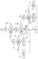
図2は、本実施形態に係るインバータ回路3の概略構成を示した回路図である。
本実施形態に係るインバータ回路3は、入力端子P、Nを介して入力される直流電力をインバータ回路3において3相交流電力に変換して、圧縮機モータ(モータ)4に供給する。なお、本実施形態では、3相交流電圧により駆動される圧縮機モータ4を駆動対象としているため、インバータ回路3の出力は3相となっているが、これに限られず、2相の出力を供給する構成とされていてもよい。
FIG. 2 is a circuit diagram showing a schematic configuration of the
The
インバータ回路3には、直流母線(電源線)Lを通じて直流電圧が供給される。
インバータ回路3は、直流電力が供給される正(P)側と負(N)側の直流母線Lと接続され、U相、V相、W相の各相に対応して設けられた上アーム回路を構成する第1スイッチング素子(第1半導体素子)U1,V1,W1と、下アーム回路を構成する第2スイッチング素子(第2半導体素子)U2,V2,W2とが直列接続された半導体モジュール(素子対)5u,5v,5wを3つ備えている。以下、特に明記しない場合には、半導体モジュールを半導体モジュール5として示す。
A DC voltage is supplied to the
The
なお、本実施形態においては、素子対5u,5v,5wをそれぞれ半導体モジュールとし、半導体モジュールを複数備えてインバータ回路3を構成することとして説明しているが、これに限定されない。例えば、素子対5u,5v,5wが1つのパッケージとなった半導体モジュールを備えてインバータ回路3を構成していてもよく、その場合には、以下の「半導体モジュール」との記載を「素子対(第1スイッチング素子と第2スイッチング素子とが直列接続されたスイッチング素子対)」と読み替える。第2の実施形態及び第3の実施形態についても同様である。
In the present embodiment, the
インバータ回路3は、直流電圧から3相交流電圧を生成し、生成した3相交流電圧を圧縮機モータ4に供給する。これらのスイッチング素子が駆動部21(後述する)により制御されることにより、圧縮機モータ4に供給される3相交流電圧(インバータ出力)が制御される。
The
電流センサ6は、直流母線Lを流れる直流電流Idcを検出し、検出された直流電流Idcをインバータ制御装置2に出力する。ここで、電流センサ6の一例としては、シャント抵抗が挙げられる。なお、図1では、電流センサ6を直流電源の負極側に設けているが、正極側に設けることとしてもよい。
インバータ制御装置2は、例えば、MPU(Micro Processing Unit)であり、以下に記載する各処理を実行するためのプログラムが記録されたコンピュータ読み取り可能な記録媒体を有しており、CPUがこの記録媒体に記録されたプログラムをRAM等の主記憶装置に読み出して実行することにより、以下の各処理が実現される。コンピュータ読み取り可能な記録媒体としては、例えば、磁気ディスク、光磁気ディスク、半導体メモリ等が挙げられる。
The
インバータ制御装置2は、圧縮機モータ4の回転数を、上位の制御装置(図示略)から与えられる回転数指令ωに一致させるようなPWM信号を相毎に生成し、インバータ回路3に与える。また、インバータ制御装置2は、インバータ回路3またはインバータ回路3を駆動する駆動部21に不具合があるか否かを判定して、判定結果を出力する。
具体的には、インバータ制御装置2は、駆動部(駆動手段)21と、電流検出部(電流検出手段)22と、不具合判定部(不具合判定手段)23と、切替部24とを備えている。
The
Specifically, the
なお、図2においては、インバータ回路3と圧縮機モータ4が接続される図を例示しているが、本第1の実施形態のインバータ制御装置2において不具合検出(故障検出)をする場合には、インバータ回路3と圧縮機モータ4とは非接続状態とされる。
FIG. 2 illustrates a diagram in which the
駆動部21は、各第1スイッチング素子U1,V1,W1及び各第2スイッチング素子U2,V2,W2のオンオフ状態を切り替える。
具体的には、駆動部21は、不具合の有無を判定する場合に、各半導体モジュール5において、第1スイッチング素子U1,V1,W1及び第2スイッチング素子U2,V2,W2を、同時に第1所定期間オン状態に制御する第1制御と、各半導体モジュール5において、上アーム回路(第1スイッチング素子U1,V1,W1)及び下アーム回路(第2スイッチング素子U2,V2,W2)のどちらか一方を第1所定期間オン状態に制御する第2制御とを行う。
The
Specifically, when determining whether or not there is a malfunction, the driving
電流検出部22は、インバータ回路3に流れる電流値を検出する。具体的には、電流センサ6から電流値の情報を取得して、電流値を検出し、検出結果を不具合判定部23に出力する。
不具合判定部23は、各半導体モジュール5において、第1スイッチング素子U1,V1,W1及び第2スイッチング素子U2,V2,W2が、同時に第1所定期間オン状態にされる第1制御、及びどちらか一方が第1所定期間オン状態にされる第2制御によって検出される電流値に基づいて、不具合の有無を判定する。また、不具合判定部23は、不具合と判定される基準となる所定の電流値(過電流)の情報を有しており、第1制御及び第2制御によって検出された電流値が過電流であるか否かに応じて、不具合があるか否かを判定する。
The
In each
なお、不具合判定部23は、少なくともいずれか一の半導体モジュール5において不具合を検出した場合に、インバータ回路3または駆動部21に不具合があると判定する。
これは、流れるはずの電流が検出されなければ開放故障とされ、流れるべきでない電流が検出されれば短絡故障とされるが、開放故障及び短絡故障であるかどうかは、半導体モジュールを構成する第1スイッチング素子U1,V1,W1または第2スイッチング素子U2,V2,W2の素子そのものに不具合が生じているケースに加え、第1スイッチング素子U1,V1,W1または第2スイッチング素子U2,V2,W2を駆動する駆動部21に不具合が生じているケースが考えられるためである。
The failure determination unit 23 determines that there is a failure in the
This is an open fault if a current that should flow is not detected, and a short circuit fault if a current that should not flow is detected. In addition to the case where the first switching elements U1, V1, W1 or the second switching elements U2, V2, W2 are defective, the first switching elements U1, V1, W1 or the second switching elements U2, V2, W2 This is because there may be a case where the
そのため、本実施形態では、インバータ回路3または駆動部21のいずれかに不具合があることとして判定するので、不具合があると判定された場合には、インバータ回路3及び駆動部21の両方を交換すれば、安全側に対処でき、確実な不具合の解消に繋がる。また、インバータ回路3を構成する半導体モジュール5のうち、1つでも不具合が検出されればインバータ回路3は正常に動作しないので、少なくとも一の半導体モジュール5で不具合が検出された場合に不具合があると判定することによって、故障検出を速やかに行うことができる。
Therefore, in this embodiment, since it is determined that either the
ここで、第1所定期間は、インバータ回路3に与えられるキャリア周波数を所定数で分割した場合の1パルス分の期間とする。
図3は、駆動部21によって第1スイッチング素子U1,V1,W1及び第2スイッチング素子U2,V2,W2をオン状態にする場合に、各スイッチング素子(第1スイッチング素子U1,V1,W1及び第2スイッチング素子U2,V2,W2)に与えるパルスの一例を示している。図3に示されるように、第1所定期間は、キャリア周波数を所定数で分割した場合の1パルス分の期間とする。例えば、キャリア周波数が5〔kHz〕とし、1周期が200〔μ秒〕とした場合には、第1所定期間は数〔μ秒〕程度とする。
また、第1所定期間が数〔μ秒〕程度であっても、各スイッチング素子のオンオフ制御によってインバータ回路3に流れる電流(すなわち、電流センサ6で検出される電流値)は、図4に示されるように、極短時間であっても急峻な電流変化が得られる程度の電流が流れる。
Here, the first predetermined period is a period of one pulse when the carrier frequency given to the
FIG. 3 illustrates the switching elements (the first switching elements U1, V1, W1, and the first switching elements) when the first switching elements U1, V1, W1 and the second switching elements U2, V2, W2 are turned on by the driving
Further, even if the first predetermined period is about several [μ seconds], the current flowing through the
ここで、不具合判定部23による不具合の判定について説明する。
本実施形態においては、半導体モジュール5毎にそれぞれ第1制御及び第2制御を行う。ここでは、第一に半導体モジュール5uに対して第1制御及び第2制御を行い、続いて半導体モジュール5v、半導体モジュール5wの順にそれぞれ第1制御及び第2制御を行うこととする。
第1制御により第1スイッチング素子U1及び第2スイッチング素子U2が同時に第1所定期間オン状態にされた場合に、通常動作(つまり、不具合が生じていない)であれば、電流センサ6で所定の電流値(例えば、図4)が計測されると推定される。これに対し、第1制御により第1スイッチング素子U1及び第2スイッチング素子U2が同時に第1所定期間オン状態にされた場合であっても、電流センサ6で所定の電流値が計測されない場合には、第1スイッチング素子U1または第2スイッチング素子U2の少なくとも一方に開放故障(オープン破壊)が生じている、或いは、U相を駆動する駆動部21に不具合が生じていると判定される。
Here, the defect determination by the defect determination unit 23 will be described.
In the present embodiment, the first control and the second control are performed for each
When the first switching element U1 and the second switching element U2 are simultaneously turned on for the first predetermined period by the first control, if the normal operation (that is, no malfunction occurs), the
また、第2制御により第1スイッチング素子U1(または第2スイッチング素子U2)を第1所定期間オン状態にされた場合、他方の第2スイッチング素子U2(または第1スイッチング素子U1)はオフ状態にされているので、通常動作(つまり、不具合が生じていない)であれば、電流センサ6で電流値は計測されないことが推定される。これに対し、第2制御により第1スイッチング素子U1(または第2スイッチング素子U2)が第1所定期間オン状態にされた場合に、電流センサ6で図4に示すような電流値が計測された場合には、他方の第2スイッチング素子U2(または第1スイッチング素子U1)に短絡故障(短絡破壊)が生じている、或いは、U相を駆動する駆動部21に不具合が生じていることと判定される。
When the first switching element U1 (or the second switching element U2) is turned on for the first predetermined period by the second control, the other second switching element U2 (or the first switching element U1) is turned off. Therefore, it is estimated that the current value is not measured by the
こうして、U相に対して第1制御及び第2制御を行い、不具合が生じていると判定された場合には、判定処理を終了して、現在のインバータ回路3及び駆動部21に不具合があることとして、判定する。
U相に対する第1制御及び第2制御で不具合が検出されない場合には、続いてV相について同様に第1制御及び第2制御を行い、V相においても不具合が検出されない場合にはW相について同様に第1制御及び第2制御を行う。
Thus, when the first control and the second control are performed on the U phase and it is determined that a problem has occurred, the determination process is terminated and the
If no trouble is detected in the first control and the second control for the U phase, the first control and the second control are performed similarly for the V phase. If no trouble is detected in the V phase, the W phase is used. Similarly, the first control and the second control are performed.
なお、インバータ制御装置2は、不具合判定を行う「テストモード」と、不具合判定を行わない「通常モード」とを有しており、切替部24によって「テストモード」と「通常モード」とが切り替え可能とされている。なお、テストモードが選択される場合には、不具合判定用のテストプログラムのみが稼働するようにしている。
切替部24は、例えば、室外機20に設けられるスイッチとし、管理者によってスイッチが押下されることによってテストモードと通常モードとが切り替えられてもよいし、リモコン40の操作部47においてテストモードを起動するためのボタン押下(例えば、通常モードでは使わない組み合わせでボタンを押下する等)によってテストモードと通常モードとが切り替えられてもよい。
Note that the
The switching
不具合判定部23による不具合の判定は、切替部24によって「テストモード」が選択された場合のみ有効とされることにより、通常の空調運転の際に、不必要に短絡電流を流すことがなく、安全である。
The determination of the defect by the defect determination unit 23 is enabled only when the “test mode” is selected by the switching
以下に本実施形態に係るインバータ制御装置2の作用について図5から図7を用いて説明する。
管理者により、インバータ回路3の不具合判定を行うテストモードが選択されると、インバータ制御装置2において、不具合判定を行うための制御プログラムが読み出される。
U相の第1スイッチング素子U1及び第2スイッチング素子U2が第1所定期間オン状態に制御される(図5のステップSA1)。過電流が検出されたか否かが判定され(図5のステップSA2)、過電流が検出されなかった場合には、第1スイッチング素子U1または第2スイッチング素子U2が開放故障している、或いは、第1スイッチング素子U1または第2スイッチング素子U2を駆動させる駆動部21が不良であると判定し(図5のステップSA3)、本処理を終了する。
The operation of the
When the administrator selects a test mode for determining a failure of the
The U-phase first switching element U1 and second switching element U2 are controlled to be in the ON state for a first predetermined period (step SA1 in FIG. 5). It is determined whether or not an overcurrent is detected (step SA2 in FIG. 5). If no overcurrent is detected, the first switching element U1 or the second switching element U2 has an open failure, or It determines with the
図5のステップSA2において、過電流が検出された場合には、第1スイッチング素子U1及び第2スイッチング素子U2をオフ状態にし(図5のステップSA4)、続いて、V相の第1スイッチング素子V1及び第2スイッチング素子V2が第1所定期間オン状態にされる(図5のステップSA5)。過電流が検出されたか否かが判定され(図5のステップSA6)、過電流が検出されなかった場合には、第1スイッチング素子V1または第2スイッチング素子V2が開放故障している、或いは、第1スイッチング素子V1または第2スイッチング素子V2を駆動させる駆動部21が不良であると判定し(図5のステップSA7)、本処理を終了する。
If an overcurrent is detected in step SA2 in FIG. 5, the first switching element U1 and the second switching element U2 are turned off (step SA4 in FIG. 5), and then the V-phase first switching element V1 and the second switching element V2 are turned on for a first predetermined period (step SA5 in FIG. 5). It is determined whether or not an overcurrent is detected (step SA6 in FIG. 5). If no overcurrent is detected, the first switching element V1 or the second switching element V2 has an open failure, or It determines with the
図5のステップSA6において、過電流が検出された場合には、第1スイッチング素子V1及び第2スイッチング素子V2をオフ状態にし(図5のステップSA8)、続いてW相の第1スイッチング素子W1及び第2スイッチング素子W2が第1所定期間オン状態にされる(図5のステップSA9)。過電流が検出されたか否かが判定され(図5のステップSA10)、過電流が検出されなかった場合には、第1スイッチング素子W1または第2スイッチング素子W2が開放故障している、或いは、第1スイッチング素子W1または第2スイッチング素子W2を駆動させる駆動部21が不良であると判定し(図5のステップSA11)、本処理を終了する。
図5のステップSA10において、過電流が検出された場合には、第1スイッチング素子W1及び第2スイッチング素子W2をオフ状態にし、第1制御を終了し(図5のステップSA12)、続いて第2制御としてU相から判定を進める(図6に進む)。
If an overcurrent is detected in step SA6 in FIG. 5, the first switching element V1 and the second switching element V2 are turned off (step SA8 in FIG. 5), and then the W-phase first switching element W1. The second switching element W2 is turned on for a first predetermined period (step SA9 in FIG. 5). It is determined whether or not an overcurrent has been detected (step SA10 in FIG. 5). If no overcurrent is detected, the first switching element W1 or the second switching element W2 has an open failure, or It determines with the
If an overcurrent is detected in step SA10 in FIG. 5, the first switching element W1 and the second switching element W2 are turned off, the first control is terminated (step SA12 in FIG. 5), and then the first As the second control, the determination proceeds from the U phase (proceed to FIG. 6).
本実施形態に係る第2制御では、第2スイッチング素子のオン制御より先に第1スイッチング素子をオン制御しているが、第1スイッチング素子のオン制御より先に第2スイッチング素子のオン制御することとしてもよい。
U相の第1スイッチング素子U1を第1所定期間オン状態にし、第2スイッチング素子U2はオフ状態のままとする(図6のステップSA13)。過電流が検出されたか否かが判定され(図6のステップSA14)、過電流が検出された場合には、第1スイッチング素子U1をオフ状態にし(図6のステップSA15)、同相の他のスイッチング素子、即ち、第2スイッチング素子U2が短絡故障、或いは第2スイッチング素子U2を駆動する駆動部21が不良であると判定し(図6のステップSA16)、本処理を終了する。
In the second control according to the present embodiment, the first switching element is turned on before the second switching element is turned on. However, the second switching element is turned on before the first switching element is turned on. It is good as well.
The U-phase first switching element U1 is turned on for a first predetermined period, and the second switching element U2 is kept off (step SA13 in FIG. 6). It is determined whether or not an overcurrent is detected (step SA14 in FIG. 6). If an overcurrent is detected, the first switching element U1 is turned off (step SA15 in FIG. 6), It is determined that the switching element, that is, the second switching element U2 is a short circuit failure, or the
図6のステップSA14において、過電流が検出されない場合には、第1スイッチング素子U1をオフ状態にし、続いて、第2スイッチング素子U2を第1所定期間オン状態にする(図6のステップSA17)。過電流が検出されたか否かが判定され(図6のステップSA18)、過電流が検出された場合には、第2スイッチング素子U2をオフ状態にし(図6のステップSA19)、他方のスイッチング素子、即ち、第1スイッチング素子U1が短絡故障、或いは第1スイッチング素子U1を駆動する駆動部21が不良であると判定し(図6のステップSA20)、本処理を終了する。
If no overcurrent is detected in step SA14 in FIG. 6, the first switching element U1 is turned off, and then the second switching element U2 is turned on for a first predetermined period (step SA17 in FIG. 6). . It is determined whether or not an overcurrent is detected (step SA18 in FIG. 6). If an overcurrent is detected, the second switching element U2 is turned off (step SA19 in FIG. 6), and the other switching element is selected. That is, it is determined that the first switching element U1 is short-circuited or the
図6のステップSA18で過電流が検出されない場合には、第2スイッチング素子U2がオフ状態にされ、続いてV相の第1スイッチング素子V1が第1所定期間オン状態にされる(図6のステップSA21)。過電流が検出されるか否かが判定され(図6のステップSA22)、過電流が検出された場合には、第1スイッチング素子V1をオフ状態にし(図6のステップSA23)、同相で他方のスイッチング素子、即ち、第2スイッチング素子V2が短絡故障、或いは第2スイッチング素子V2を駆動する駆動部21が不良であると判定し(図6のステップSA24)、本処理を終了する。
図6のステップSA22において、過電流が発生していない場合には、第1スイッチング素子V1をオフ状態にし、続いて第2スイッチング素子V2を第1所定期間オン状態にする(図6のステップSA25)。
If no overcurrent is detected in step SA18 of FIG. 6, the second switching element U2 is turned off, and then the V-phase first switching element V1 is turned on for a first predetermined period (FIG. 6). Step SA21). It is determined whether or not an overcurrent is detected (step SA22 in FIG. 6). If an overcurrent is detected, the first switching element V1 is turned off (step SA23 in FIG. 6), and the other in the same phase. The switching element, that is, the second switching element V2 is short-circuited or the
In step SA22 in FIG. 6, if no overcurrent has occurred, the first switching element V1 is turned off, and then the second switching element V2 is turned on for a first predetermined period (step SA25 in FIG. 6). ).
過電流が検出されたか否かが判定され(図7のステップSA26)、過電流が検出された場合には、第2スイッチング素子V2をオフ状態にし(図7のステップSA27)、同相で他方のスイッチング素子、即ち第1スイッチング素子V1が短絡故障、或いは、第1スイッチング素子V1を駆動する駆動部21が不良であると判定し(図7のステップSA28)、本処理を終了する。
It is determined whether or not an overcurrent is detected (step SA26 in FIG. 7). If an overcurrent is detected, the second switching element V2 is turned off (step SA27 in FIG. 7). It is determined that the switching element, that is, the first switching element V1 is a short circuit failure, or the
図7のステップSA26で過電流が検出されない場合には、第2スイッチング素子V2をオフ状態にし、続いてW相の第1スイッチング素子W1を第1所定期間オン状態にする(図7のステップSA29)。過電流が検出されるか否かが判定され(図7のステップSA30)、過電流が検出された場合には、第1スイッチング素子W1がオフ状態にされ(図7のステップSA31)、同相で他方のスイッチング素子、即ち、第2スイッチング素子W2が短絡故障している、或いは第2スイッチング素子W2を駆動する駆動部21が不良であると判定し(図7のステップSA32)、本処理を終了する。
If no overcurrent is detected in step SA26 in FIG. 7, the second switching element V2 is turned off, and then the W-phase first switching element W1 is turned on for a first predetermined period (step SA29 in FIG. 7). ). It is determined whether or not an overcurrent is detected (step SA30 in FIG. 7). If an overcurrent is detected, the first switching element W1 is turned off (step SA31 in FIG. 7) and is in phase. It is determined that the other switching element, that is, the second switching element W2 has a short-circuit failure, or that the
図7のステップSA30で過電流が検出されない場合には、第1スイッチング素子W1をオフ状態にし、第2スイッチング素子W2を第1所定期間オン状態にする(図7のステップSA33)。過電流が検出されたか否かが判定され(図7のステップSA34)、過電流が検出された場合には、第2スイッチング素子W2をオフ状態にし(図7のステップSA35)、同相で他方のスイッチング素子、即ち、第1スイッチング素子W1が短絡故障している、或いは、第1スイッチング素子W1を駆動する駆動部21が不良であると判定し(図7のステップSA36)、本処理を終了する。
なお、図7のステップSA34において、過電流が検出されなかった場合には、インバータ回路3は正常であると判定し、本処理を終了する(図7のステップSA37)。
If no overcurrent is detected in step SA30 in FIG. 7, the first switching element W1 is turned off and the second switching element W2 is turned on for a first predetermined period (step SA33 in FIG. 7). It is determined whether or not an overcurrent has been detected (step SA34 in FIG. 7). If an overcurrent is detected, the second switching element W2 is turned off (step SA35 in FIG. 7), It is determined that the switching element, that is, the first switching element W1 has a short circuit failure, or the
If no overcurrent is detected in step SA34 in FIG. 7, it is determined that the
判定結果は、室外機20の基板上のLED,7セグメントLED等の表示部8で不具合(故障)表示するようにしてもよいし、通信を介して室内機30に不具合(故障)の情報を送信して表示部31上で表示させてもよいし、通信を介してリモコン40に不具合(故障)の情報を送信して表示部46上で表示させてもよい。
これにより、室外機20、室内機30、及びリモコン40のいずれかを確認することにより、管理者が不具合の有無を速やかに把握できる。
The determination result may be displayed as a failure (failure) on the
Thereby, by confirming any of the
以上説明してきたように、本実施形態に係るインバータ制御装置2、それを備えた空気調和装置100、及び故障検出方法並びにプログラムによれば、各半導体モジュール5において、第1制御をすると、不具合がなければ、第1スイッチング素子U1,V1,W1と第2スイッチング素子U2,V2,W2とを通じて電流が流れるので、インバータ回路3には電流が流れることが推定されるが、所望の電流値が検出されなければ不具合(例えば、開放故障または駆動部21の故障)が生じていると判定される。また、各半導体モジュール5において、第2制御をすると、圧縮機モータ4はインバータ回路3と未接続状態とされており、不具合がなければ、一方のスイッチング素子がオフ状態にされているので、インバータ回路3に電流が流れないことが推定されるが、電流が検出されれば不具合(例えば、短絡故障または駆動部21の故障)が生じていると判定される。
As described above, according to the
このように、本実施形態によれば、第1制御または第2制御を行った場合に検出されるインバータ回路3の電流値に基づいて、簡便にインバータ回路3の不具合有無を検出できる。また、本実施形態によれば、従来用いていた異常判定機器が不要となるので、異常判定機器の配備やメンテナンスが不要になり、異常判定機器の費用も不要となる。
また、第1スイッチング素子U1,V1,W1または第2スイッチング素子U2,V2,W2の1つずつをオン状態に切り換えて故障を検出する第2制御においては、不具合箇所が明確になり、確実な検査を行うことができる。
なお、第2制御より第1制御を先に行う方が、不具合(故障)有無の切り分けを簡便にすることができるので、本実施形態においては、第2制御よりも先に第1制御を行っている。
As described above, according to the present embodiment, it is possible to easily detect whether or not the
Further, in the second control in which the failure is detected by switching one of the first switching elements U1, V1, W1 or the second switching elements U2, V2, W2 one by one, the trouble location becomes clear and reliable. Inspection can be performed.
In addition, in the present embodiment, the first control is performed prior to the second control because the first control prior to the second control can simplify the determination of the presence or absence of a malfunction (failure). ing.
〔第2の実施形態〕
次に、本発明の第2の実施形態について図1、図2及び図8から図11を用いて説明する。本実施形態は、インバータ制御装置2において故障検出をするにあたり、インバータ回路3と圧縮機モータ4とが接続状態とされている点と第3制御を行う点で、上述した第1の実施形態と異なる。以下、本実施形態について、第1の実施形態と共通する点については説明を省略し、異なる点について主に説明する。
[Second Embodiment]
Next, a second embodiment of the present invention will be described with reference to FIGS. 1, 2, and 8 to 11. FIG. The present embodiment is different from the first embodiment described above in that the
本第2の実施形態においては、インバータ制御装置2において故障検出をするにあたり、インバータ回路3と圧縮機モータ4とは接続状態とされている。
In the second embodiment, the
不具合判定部23は、各半導体モジュール5u,5v,5wにおいて、第1スイッチング素子U1,V1,W1及び第2スイッチング素子U2,V2,W2が、同時に第1所定期間オン状態にされる第1制御、及びいずれか一の半導体モジュール5u,5v,5wの上アーム下アームどちらか一方のスイッチング素子が第1所定期間オン状態にされる第2制御によって検出される電流値に基づいて、不具合の有無を判定する。
また、不具合判定部23は、いずれか一の半導体モジュール5u,5v,5wの上アーム下アームどちらか一方のスイッチング素子を第1所定期間オン状態にしても第1所定値以上の電流値が検出されない場合には、第1所定期間より長い期間である第2所定期間オン状態にする第3制御をし、第3制御の結果、第2所定値以上の電流値が検出されれば、他の半導体モジュール5u,5v,5wの(オン状態にしたスイッチング素子のアームとは逆側の)スイッチング素子に不具合があると判定する。
In the
In addition, the failure determination unit 23 detects a current value greater than or equal to the first predetermined value even if any one of the switching elements of the upper arms and lower arms of the
ここで、第1所定期間は、インバータ回路3に与えられるキャリア周波数を所定数で分割した場合の1パルス分の期間とし、第2所定期間は、1パルス分の期間を第1所定期間より長く設定する(図8参照)。
なお、本実施形態においては、第2所定期間は、1パルス分の期間を第1所定期間より長く設定することとして説明するが、これに限定されず、例えば、第1所定期間で与えられる1パルスを複数パルス(例えば、10パルス)与え、第2所定期間としてもよい。
Here, the first predetermined period is a period corresponding to one pulse when the carrier frequency supplied to the
In the present embodiment, the second predetermined period is described as setting a period of one pulse longer than the first predetermined period. However, the present invention is not limited to this. For example, the first predetermined period is given as 1 A plurality of pulses (for example, 10 pulses) may be given for the second predetermined period.
図9には、第3制御において、第2所定期間スイッチング素子をオン状態にした場合に得られる時間と電流値との関係の一例が示されている。
上述したように、第3制御をする場合には、各相と圧縮機モータ4とが図2に示されるように接続状態にされているので、例えば、U相の第2スイッチング素子U2をオフ状態にし、第1スイッチング素子U1を第2所定期間オン状態にした場合に、正常動作(つまり、不具合がない)の場合には電流センサ6による電流値は検出されないが、圧縮機モータ4を介して接続される他相(例えば、V相、W相)に短絡故障が生じている場合には、電流センサ6によって電流値が検出される。このとき、圧縮機モータ4を通して電流が流れると、インダクタンス成分等の影響によって、電流センサ6から検出される電流値は徐々に上昇する(図9参照)。
FIG. 9 shows an example of the relationship between the time and the current value obtained when the switching element is turned on for the second predetermined period in the third control.
As described above, when the third control is performed, each phase and the
このように、第3制御の場合に検出される電流値の時間変化は、第1制御及び第2制御と比較して緩やかになるので、第3制御における電流値の時間変化に基づいて過電流か否かを判定する場合には、この点を勘案するとよい。なお、第3制御における電流値の時間変化(つまり、時間に対する電流値の傾き)は、インバータ回路3に接続されるモータに応じて制御チューニングする必要がある。
As described above, the time change of the current value detected in the case of the third control becomes gentler than that of the first control and the second control. Therefore, the overcurrent is based on the time change of the current value in the third control. This point should be taken into consideration when determining whether or not. The time change of the current value in the third control (that is, the slope of the current value with respect to time) needs to be controlled and tuned according to the motor connected to the
以下に本実施形態に係るインバータ制御装置2の作用について図2から図10及び図11を用いて説明する。なお、本実施形態における第1制御は、第1の実施形態と同様であるため(図5参照)、説明を省略し、本実施形態の第2制御の開始から説明をする。
第1制御で不具合がないと判定されると(図5参照)、図10に進み、U相の第1スイッチング素子U1を第1所定期間オン状態にする(図10のステップSB1)。過電流が検出されたか否かが判定され(図10のステップSB2)過電流が検出された場合には第1スイッチング素子U1をオフ状態にし(図10のステップSB3)、同相の他方のスイッチング素子、即ち第2スイッチング素子U2が短絡故障している、或いは第2スイッチング素子U2を駆動させる駆動部21が不良であると判定され(図10のステップSB4)、本処理を終了する。
Hereinafter, the operation of the
If it is determined that there is no problem in the first control (see FIG. 5), the process proceeds to FIG. 10, and the U-phase first switching element U1 is turned on for a first predetermined period (step SB1 in FIG. 10). It is determined whether or not an overcurrent is detected (step SB2 in FIG. 10). If an overcurrent is detected, the first switching element U1 is turned off (step SB3 in FIG. 10), and the other switching element in the same phase That is, it is determined that the second switching element U2 is short-circuited or the
図10のステップSB2において、過電流が検出されない場合には、第1スイッチング素子U1を一旦オフ状態にし、第1スイッチング素子U1を第2所定期間オン状態にする(図10のステップSB5)。第2所定期間オン状態にすることにより過電流が検出されたか否かが判定され(図10のステップSB6)、過電流が検出された場合には、第1スイッチング素子U1をオフ状態にし(図10のステップSB7)、他相かつ他アームのスイッチング素子、即ち、圧縮機モータ4を介して接続状態にされるV相の第2スイッチング素子V2またはW相の第2スイッチング素子W2が短絡故障している、或いは、V相の第2スイッチング素子V2またはW相の第2スイッチング素子W2を駆動する駆動部21が不良であると判定される(図10のステップSB8)。
If no overcurrent is detected in step SB2 of FIG. 10, the first switching element U1 is temporarily turned off and the first switching element U1 is turned on for a second predetermined period (step SB5 of FIG. 10). It is determined whether or not an overcurrent has been detected by turning on the second predetermined period (step SB6 in FIG. 10). If an overcurrent is detected, the first switching element U1 is turned off (see FIG. 10). 10 step SB7), the switching element of the other phase and the other arm, that is, the second switching element V2 of the V phase or the second switching element W2 of the W phase which is connected via the
図10のステップSB6において、過電流が検出されない場合には、第1スイッチング素子U1をオフ状態にし、第2スイッチング素子U2を第1所定期間オン状態にする(図10のステップSB9)。過電流が検出されるか否かが判定され(図11のステップSB10)、過電流が検出された場合には、第2スイッチング素子U2をオフ状態にし(図11のステップSB11)、同相で他方のスイッチング素子、即ち、第1スイッチング素子U1が短絡故障している或いは第1スイッチング素子U1を駆動する駆動部21が不良であると判定される(図11のステップSB12)。
If no overcurrent is detected in step SB6 in FIG. 10, the first switching element U1 is turned off and the second switching element U2 is turned on for a first predetermined period (step SB9 in FIG. 10). It is determined whether or not an overcurrent is detected (step SB10 in FIG. 11). If an overcurrent is detected, the second switching element U2 is turned off (step SB11 in FIG. 11), and the other is in phase. That is, it is determined that the first switching element U1 is short-circuited or the
図11のステップSB10において、過電流が検出されない場合には、第2スイッチング素子U2を一旦オフ状態にし、その後第2スイッチング素子U2の第2所定期間オン状態にする(図11のステップSB13)。過電流が検出されたか否かが判定され(図11のステップSB14)、過電流が検出された場合には、第2スイッチング素子U2をオフ状態にし(図11のステップSB15)、他相の第1スイッチング素子V1または第1スイッチング素子W1が短絡故障している、或いは他相の第1スイッチング素子V1または第1スイッチング素子W1を駆動する駆動部21が不良であると判定される(図11のステップSB16)。
なお、図11のステップSB14において、過電流が検出されない場合には、インバータ回路3は正常であると判定され(図11のステップSB17)、本処理を終了する。
If no overcurrent is detected in step SB10 of FIG. 11, the second switching element U2 is temporarily turned off, and then the second switching element U2 is turned on for a second predetermined period (step SB13 of FIG. 11). It is determined whether or not an overcurrent is detected (step SB14 in FIG. 11). If an overcurrent is detected, the second switching element U2 is turned off (step SB15 in FIG. 11), It is determined that the first switching element V1 or the first switching element W1 has a short circuit failure, or the driving
If no overcurrent is detected in step SB14 in FIG. 11, it is determined that the
以上説明してきたように、本実施形態に係るインバータ制御装置2、それを備えた空気調和装置100、及び故障検出方法並びにプログラムによれば、第1スイッチング素子U1,V1,W1と第2スイッチング素子U2,V2,W2とが直列に接続された半導体モジュール5が複数備えられ、正負の直流母線Lから供給された直流電力を交流電力に変換して圧縮機モータ4に電力供給するインバータ回路3のインバータ制御装置2は各半導体モジュール5において、第1制御をすると不具合がなければ、第1スイッチング素子U1,V1,W1と第2スイッチング素子U2,V2,W2とを通じて電流が流れるので、インバータ回路3には電流が流れることが推定されるが、所望の電流値が検出されなければ不具合(例えば、開放故障)が生じていると判定される。
As explained above, according to the
また、各半導体モジュール5において、第2制御をすると、同相の他方のスイッチング素子はオフ状態にされているので、不具合がなければ、インバータ回路3に電流が流れないことが推定されるが、電流が検出されれば不具合(例えば、短絡故障)が生じていると判定される。
さらに、第2制御によって電流が検出されなくても、第3制御によって電流が検出されると、他相の半導体モジュール5を構成するスイッチング素子に電流が流れることを示すので、こうした場合には他の半導体モジュール5を構成するスイッチング素子に不具合(例えば、短絡故障)が含まれると判定される。なお、このとき検出される電流は、接続される圧縮機モータ4のインダクタンス成分等の影響により、第1制御及び第2制御より緩やかな変化率となる。
In each
Furthermore, even if the current is not detected by the second control, if the current is detected by the third control, it indicates that the current flows through the switching elements constituting the
このように、本実施形態によれば、インバータ回路3を構成する半導体モジュール5を第1制御、第2制御、及び第3制御し、インバータ回路3に流れる電流値に基づいて、簡便にインバータ回路3の不具合有無を検出できる。
本実施形態の構成では、インバータ回路3に圧縮機モータ4を接続したまま検査することができるので、第1の実施形態で示される圧縮機モータ4を未接続として検査する場合と比較して、圧縮機モータ4を取り外す作業が省略でき、不具合検出手順が簡便となる。
As described above, according to the present embodiment, the
In the configuration of the present embodiment, since the
〔第3の実施形態〕
次に、本発明の第3の実施形態について図1、図2及び図11を用いて説明する。本実施形態に係るインバータ制御装置2は、第2制御において、スイッチング素子をオン状態にする場合のパルスのオン期間を指定せず、過電流が検出された場合に過電流が検出された期間の長さに応じて不具合箇所の判定を異ならせる点で、上述した第1の実施形態、第2の実施形態と異なる。以下、本実施形態について、第1の実施形態、第2の実施形態と共通する点については説明を省略し、異なる点について主に説明する。
[Third Embodiment]
Next, a third embodiment of the present invention will be described with reference to FIGS. In the second control, the
不具合判定部23は、電流値が第1所定値以上となるまでの期間である第2所定期間が所定時間未満であれば、オン状態にしたスイッチング素子と同一の半導体モジュール5u,5v,5wにおけるオフ状態のスイッチング素子の不具合と判定し、第2所定期間が所定時間以上であれば、オン状態にしたスイッチング素子と異なる半導体モジュール5における(オン状態にしたアームと逆側のアームの)スイッチング素子の不具合と判定する。
If the second predetermined period, which is a period until the current value becomes equal to or greater than the first predetermined value, is less than the predetermined time, the defect determination unit 23 determines that the
以下に本実施形態に係るインバータ制御装置2の作用について図2及び図12を用いて説明する。なお、本実施形態における第1制御は、第1の実施形態、第2の実施形態と同様であるため、説明を省略し(図5参照)、本第3実施形態の第2制御の開始から説明をする。
第1制御により不具合がないと判定されると(図5参照)、続いて、U相の第1スイッチング素子U1がオン状態にされる(図12のステップSC1)。過電流が検出されたか否かが判定され(図12のステップSC2)、過電流が検出された場合に第1スイッチング素子U1がオフ状態にされる(図12のステップSC3)。検出された過電流が所定時間内か否かが判定され(図12のステップSC4)、過電流が流れた時間が所定時間未満であれば、第2スイッチング素子U2が短絡破壊または第2スイッチング素子U2を駆動する駆動部21が不良であると判定され(図12のステップSC5)、本処理を終了する。
Below, the effect | action of the
If it is determined by the first control that there is no malfunction (see FIG. 5), then, the U-phase first switching element U1 is turned on (step SC1 in FIG. 12). It is determined whether or not an overcurrent is detected (step SC2 in FIG. 12), and when the overcurrent is detected, the first switching element U1 is turned off (step SC3 in FIG. 12). It is determined whether or not the detected overcurrent is within a predetermined time (step SC4 in FIG. 12). If the time during which the overcurrent flows is less than the predetermined time, the second switching element U2 is short-circuit broken or the second switching element. It is determined that the
また、過電流が流れた時間が所定時間以上である場合には、オン状態にされたスイッチング素子とは異なる相の他方のスイッチング素子(例えば、V相の第2スイッチング素子V2またはW相の第2スイッチング素子W2)において、短絡破壊またはそれらスイッチング素子を駆動する駆動部21が不良であると判定される(図12のステップSC6)。
また、図12のステップSC2において、過電流が発生していないと判定された場合には、第1スイッチング素子U1をオフ状態にし、第2スイッチング素子U2をオン状態にする(図12のステップSC7)。過電流が検出されたか否かが判定され(図12のステップSC8)、過電流が発生した場合には、第2スイッチング素子U2がオフ状態にされ(図12のステップSC9)過電流が所定時間内か否かが判定される(図12のステップSC10)。
When the overcurrent flows for a predetermined time or more, the other switching element of a phase different from the switching element that is turned on (for example, the V-phase second switching element V2 or the W-phase first switching element). In the two switching elements W2), it is determined that the short circuit breakage or the
If it is determined in step SC2 in FIG. 12 that no overcurrent has occurred, the first switching element U1 is turned off and the second switching element U2 is turned on (step SC7 in FIG. 12). ). It is determined whether or not an overcurrent has been detected (step SC8 in FIG. 12). If an overcurrent has occurred, the second switching element U2 is turned off (step SC9 in FIG. 12), and the overcurrent is maintained for a predetermined time. It is determined whether it is within (step SC10 in FIG. 12).
過電流が所定時間未満であれば、他方のスイッチング素子である第1スイッチング素子U1の短絡破壊、または第1スイッチング素子U1を駆動する駆動部21が不良であると判定される(図12のステップSC11)。図12のステップSC10において、過電流が所定時間以上であると判定された場合には、他相の他アームのスイッチング素子であるV相の第1スイッチング素子V1またはW相の第1スイッチング素子W1が短絡故障しているか、駆動させる駆動部21が不良であると判定される(図12のステップSC12)。
なお、図12のステップSC8において、過電流が検出されなかった場合には、インバータ回路3は正常であると判定される(図12のステップSC13)。
If the overcurrent is less than the predetermined time, it is determined that the first switching element U1, which is the other switching element, is short-circuited or that the
If no overcurrent is detected in step SC8 in FIG. 12, it is determined that
以上説明してきたように、本実施形態に係るインバータ制御装置2、それを備えた空気調和装置100、及び故障検出方法並びにプログラムによれば、第2所定期間が、所定値未満であれば、オン状態に制御した半導体モジュール5と同じ半導体モジュール5の他のスイッチング素子に不具合があると判定され、第2所定期間が所定値以上であれば、オン状態に制御した半導体モジュール5と異なる半導体モジュール5における他のアーム側のスイッチング素子に不具合があると判定される。
このように、本実施形態によれば、インバータ回路3を構成する半導体モジュールの第1半導体素子及び第2半導体素子を同時に第1所定期間オン状態、或いは一方を第2所定期間オン状態に切り替えた場合に検出されるインバータ回路3の電流値に基づいて、簡便にインバータ回路の不具合有無を検出できる。
As described above, according to the
Thus, according to the present embodiment, the first semiconductor element and the second semiconductor element of the semiconductor module constituting the
また、本発明によれば、従来用いていた異常判定機器が不要となるので、異常判定機器の配備やメンテナンスが不要になり、異常判定機器の費用も不要となる。
また、本実施形態のように、スイッチング素子に与えるパルスは時間を指定しなくても、所望の過電流が検出された時点でスイッチング素子をオフにして、それまでにパルスがオンされた時間を遡って確認するので、パルスの時間制御をする必要がなく、簡便に検査できる。
また、本第3の実施形態の構成に示したように、インバータ回路3に圧縮機モータ4を接続したまま検査することができるので、圧縮機モータ4が未接続となっている検査の場合と比較して、圧縮機モータ4を取り外す作業が省略でき、不具合検出手順が簡便となる。
Further, according to the present invention, since the abnormality determining device that has been used conventionally is not required, the deployment and maintenance of the abnormality determining device is unnecessary, and the cost of the abnormality determining device is also unnecessary.
Further, as in this embodiment, even if the pulse given to the switching element does not specify a time, the switching element is turned off when a desired overcurrent is detected, and the time when the pulse is turned on until then is determined. Since it is confirmed retroactively, it is not necessary to control the time of the pulse, and the inspection can be performed easily.
Further, as shown in the configuration of the third embodiment, since the
本発明は上述した実施形態に限定されることはなく、その要旨を逸脱しない範囲内において適宜変更することができる。 The present invention is not limited to the above-described embodiment, and can be changed as appropriate without departing from the scope of the invention.
2 インバータ制御装置(故障検出装置を含む)
3 インバータ回路
4 圧縮機モータ
5u,5v,5w 半導体モジュール(素子対)
6 電流センサ
21 駆動部
22 電流検出部
23 不具合判定部
24 切替部
U1,V1,W1 第1スイッチング素子
U2,V2,W2 第2スイッチング素子
2 Inverter control device (including failure detection device)
3
6
Claims (8)
前記モータと前記インバータ回路とが接続状態とされ、
前記インバータ回路は、前記直流電力が供給される正負の電源線と接続され、上アーム回路を構成する半導体素子である第1半導体素子と下アーム回路を構成する前記半導体素子である第2半導体素子とが直列に接続された素子対を複数備えており、
各前記第1半導体素子及び各前記第2半導体素子のオンオフ状態を切り替える駆動手段と、
前記インバータ回路に流れる電流値を検出する電流検出手段と、
各前記素子対において、前記第1半導体素子及び前記第2半導体素子が、同時に第1所定期間オン状態にされる第1制御、及びどちらか一方がオン状態にされる第2制御によって検出される前記電流値に基づいて、不具合の有無を判定する不具合判定手段とを具備し、
前記不具合判定手段は、前記電流値が第1所定値以上となるまでの期間である第2所定期間が所定時間未満であれば、オン状態にした前記半導体素子と同一前記素子対におけるオフ状態の前記半導体素子の不具合と判定し、前記第2所定期間が所定時間以上であれば、オン状態にした半導体素子と異なる前記素子対における前記半導体素子の不具合と判定する故障検出装置。 A failure detection device for an inverter circuit that converts DC power into AC power and supplies power to the motor,
The motor and the inverter circuit are connected,
The inverter circuit is connected to positive and negative power supply lines to which the DC power is supplied, and a first semiconductor element which is a semiconductor element constituting an upper arm circuit and a second semiconductor element which is the semiconductor element constituting a lower arm circuit And a plurality of element pairs connected in series,
Driving means for switching on and off states of each of the first semiconductor elements and each of the second semiconductor elements;
Current detecting means for detecting a current value flowing through the inverter circuit;
In each of the element pairs, the first semiconductor element and the second semiconductor element are detected by the first control in which the first semiconductor element and the second semiconductor element are simultaneously turned on for the first predetermined period and the second control in which one of them is turned on. A failure determination means for determining the presence or absence of a failure based on the current value;
If the second predetermined period, which is a period until the current value becomes equal to or greater than the first predetermined value, is less than a predetermined time, the defect determining means determines that the off state in the same element pair as the semiconductor element in the on state A failure detection device that determines that the semiconductor element is defective, and determines that the semiconductor element is defective in the element pair different from the semiconductor element that is turned on if the second predetermined period is equal to or longer than a predetermined time.
前記不具合判定手段は、前記テストモードが選択された場合のみ有効とされる請求項1から請求項3のいずれかに記載の故障検出装置。 The inverter circuit can be switched between a test mode for performing a failure determination and a normal mode in which the failure determination is not performed.
It said fault judging means, the failure detection device according to any one of claims 1 to 3, wherein the test mode is effective only when it is selected.
前記短絡故障よりも先に前記開放故障を検査する請求項1から請求項4に記載のいずれかに故障検出装置。 The failure detected by the first control is an open failure, the failure detected by the second control is a short-circuit failure,
Failure detection device to any according to claims 1 to 4 for inspecting the open-circuit failure earlier than the short-circuit failure.
上アーム回路及び下アーム回路の直列回路を内蔵した素子対が複数設けられ、かつ、各前記素子対は、前記上アーム回路を構成する第1半導体素子と、前記下アーム回路を構成する第2半導体素子とを備えるインバータ回路と、
前記インバータ回路の負荷であり、空気調和装置の圧縮機を駆動するモータと、
を具備する空気調和装置。 A fault detection device for an inverter circuit according to any one of claims 1 to 5 ,
A plurality of element pairs each including a series circuit of an upper arm circuit and a lower arm circuit are provided, and each of the element pairs includes a first semiconductor element constituting the upper arm circuit and a second semiconductor element constituting the lower arm circuit. An inverter circuit comprising a semiconductor element;
A motor that is a load of the inverter circuit and drives a compressor of the air conditioner;
An air conditioner comprising:
前記モータと前記インバータ回路とが接続状態とされ、
前記インバータ回路は、前記直流電力が供給される正負の電源線と接続され、上アーム回路を構成する半導体素子である第1半導体素子と下アーム回路を構成する前記半導体素子である第2半導体素子とが直列に接続された素子対を複数備えており、
各前記第1半導体素子及び各前記第2半導体素子のオンオフ状態を切り替える第1過程と、
前記インバータ回路に流れる電流値を検出する第2過程と、
各前記素子対において、前記第1半導体素子及び前記第2半導体素子が、同時に第1所定期間オン状態にされる第1制御、及びどちらか一方が第2所定期間オン状態にされる第2制御によって検出される前記電流値に基づいて、不具合の有無を判定する第3過程とを具備し、
前記第3過程は、前記電流値が第1所定値以上となるまでの期間である第2所定期間が所定時間未満であれば、オン状態にした前記半導体素子と同一前記素子対におけるオフ状態の前記半導体素子の不具合と判定し、前記第2所定期間が所定時間以上であれば、オン状態にした前記半導体素子と異なる前記素子対における前記半導体素子の不具合と判定する故障検出方法。 A failure detection method for an inverter circuit that converts DC power into AC power and supplies power to the motor,
The motor and the inverter circuit are connected,
The inverter circuit is connected to positive and negative power supply lines to which the DC power is supplied, and a first semiconductor element which is a semiconductor element constituting an upper arm circuit and a second semiconductor element which is the semiconductor element constituting a lower arm circuit And a plurality of element pairs connected in series,
A first step of switching on and off states of each of the first semiconductor elements and each of the second semiconductor elements;
A second process of detecting a current value flowing through the inverter circuit;
In each of the element pairs, the first control in which the first semiconductor element and the second semiconductor element are simultaneously turned on for a first predetermined period, and the second control in which one is turned on for a second predetermined period. A third step of determining the presence or absence of a defect based on the current value detected by
In the third process, if the second predetermined period, which is a period until the current value becomes equal to or higher than the first predetermined value, is less than a predetermined time, the off state in the same element pair as the semiconductor element in the on state is determined. A failure detection method for determining a failure of the semiconductor element and determining that the semiconductor element has a failure in the element pair different from the semiconductor element in an on state if the second predetermined period is equal to or longer than a predetermined time.
前記モータと前記インバータ回路とが接続状態とされ、
各第1半導体素子及び各第2半導体素子のオンオフ状態を切り替える第1処理と、
前記直流電力が供給される正負の電源線と接続され、上アーム回路を構成する半導体素子である第1半導体素子と下アーム回路を構成する前記半導体素子である第2半導体素子とが直列に接続された素子対を複数備えているインバータ回路に流れる電流値を検出する第2処理と、
各前記素子対において、前記第1半導体素子及び前記第2半導体素子が、同時に第1所定期間オン状態にされる第1制御、及びどちらか一方が第2所定期間オン状態にされる第2制御によって検出される前記電流値に基づいて、不具合の有無を判定する第3処理とをコンピュータに実行させ、
前記第3処理は、前記電流値が第1所定値以上となるまでの期間である第2所定期間が所定時間未満であれば、オン状態にした前記半導体素子と同一前記素子対におけるオフ状態の前記半導体素子の不具合と判定し、前記第2所定期間が所定時間以上であれば、オン状態にした前記半導体素子と異なる前記素子対における前記半導体素子の不具合と判定するための故障検出プログラム。 A fault detection program for an inverter circuit that converts DC power into AC power and supplies power to the motor,
The motor and the inverter circuit are connected,
A first process for switching on and off states of each first semiconductor element and each second semiconductor element;
A first semiconductor element, which is a semiconductor element constituting the upper arm circuit, and a second semiconductor element, which is the semiconductor element constituting the lower arm circuit, are connected in series to the positive and negative power supply lines to which the DC power is supplied. A second process for detecting a current value flowing in an inverter circuit including a plurality of element pairs,
In each of the element pairs, the first control in which the first semiconductor element and the second semiconductor element are simultaneously turned on for a first predetermined period, and the second control in which one is turned on for a second predetermined period. A third process for determining the presence or absence of a defect based on the current value detected by the computer,
In the third process, if the second predetermined period, which is a period until the current value becomes equal to or higher than the first predetermined value, is less than a predetermined time, the off state in the same element pair as the semiconductor element in the on state is determined. A failure detection program for determining a defect of the semiconductor element and determining that the defect of the semiconductor element in the element pair is different from the semiconductor element turned on when the second predetermined period is equal to or longer than a predetermined time.
Priority Applications (1)
| Application Number | Priority Date | Filing Date | Title |
|---|---|---|---|
| JP2014225279A JP6396177B2 (en) | 2014-11-05 | 2014-11-05 | Failure detection device, air conditioner including the same, failure detection method and program |
Applications Claiming Priority (1)
| Application Number | Priority Date | Filing Date | Title |
|---|---|---|---|
| JP2014225279A JP6396177B2 (en) | 2014-11-05 | 2014-11-05 | Failure detection device, air conditioner including the same, failure detection method and program |
Publications (2)
| Publication Number | Publication Date |
|---|---|
| JP2016092977A JP2016092977A (en) | 2016-05-23 |
| JP6396177B2 true JP6396177B2 (en) | 2018-09-26 |
Family
ID=56019262
Family Applications (1)
| Application Number | Title | Priority Date | Filing Date |
|---|---|---|---|
| JP2014225279A Expired - Fee Related JP6396177B2 (en) | 2014-11-05 | 2014-11-05 | Failure detection device, air conditioner including the same, failure detection method and program |
Country Status (1)
| Country | Link |
|---|---|
| JP (1) | JP6396177B2 (en) |
Families Citing this family (2)
| Publication number | Priority date | Publication date | Assignee | Title |
|---|---|---|---|---|
| KR102337700B1 (en) | 2017-03-17 | 2021-12-08 | 엘에스일렉트릭(주) | diagnosing device of three phase inverter |
| US12301130B2 (en) | 2021-07-07 | 2025-05-13 | Tmeic Corporation | Power conversion device and method of diagnosing failures of switching devices |
Family Cites Families (3)
| Publication number | Priority date | Publication date | Assignee | Title |
|---|---|---|---|---|
| JPS6331478A (en) * | 1986-07-24 | 1988-02-10 | Toshiba Corp | Troubleshooting device for inverter |
| JPH07114548B2 (en) * | 1988-05-30 | 1995-12-06 | ダイキン工業株式会社 | Inverter pulse width modulation controller |
| JP4438833B2 (en) * | 2007-07-04 | 2010-03-24 | トヨタ自動車株式会社 | Abnormality detection apparatus and abnormality detection method for power converter |
-
2014
- 2014-11-05 JP JP2014225279A patent/JP6396177B2/en not_active Expired - Fee Related
Also Published As
| Publication number | Publication date |
|---|---|
| JP2016092977A (en) | 2016-05-23 |
Similar Documents
| Publication | Publication Date | Title |
|---|---|---|
| JP6831023B2 (en) | Inverter device | |
| CN109863685B (en) | Air conditioner and drive device | |
| EP3093984B1 (en) | Power conversion device | |
| CN108604876B (en) | motor control device | |
| JP2016144226A (en) | Motor drive device with change function for current detection mode | |
| JP6396177B2 (en) | Failure detection device, air conditioner including the same, failure detection method and program | |
| CN111727557B (en) | Motor drives and refrigeration cycle application equipment | |
| CN104682682A (en) | Identifying Function Defect Of At Least One Active Switch Element Of Active Bridge Rectifier | |
| CN110915127B (en) | Air conditioner | |
| EP1796255B1 (en) | Air conditioner | |
| JP6402788B2 (en) | Power converter | |
| JP4155307B2 (en) | Control device for air conditioner | |
| KR101195157B1 (en) | Motor Controlling Inverter Having Function For Sensing Mis-Wiring | |
| JP2006054943A (en) | Power converter and failure diagnosing method for same | |
| JP5001642B2 (en) | Electric motor drive device and phase loss detection method thereof | |
| US12525855B2 (en) | Methods and circuits for line synchronization during transition of an electric motor between variable frequency inverter power and line frequency power | |
| JP2014143782A (en) | Motor control device | |
| CN101599703B (en) | Method for converting three-phase power supply into single-phase voltage output and AC power supply | |
| JP2015002659A (en) | Inverter device inspection method | |
| JP2006141114A (en) | Air conditioner control device | |
| CN115684753A (en) | Test circuit and method for soft start module in frequency converter | |
| JP2011117622A (en) | Controlling device of air conditioner | |
| JP2008236896A (en) | Air conditioner control device | |
| JP2010035318A (en) | Drive system of brushless motor |
Legal Events
| Date | Code | Title | Description |
|---|---|---|---|
| A621 | Written request for application examination |
Free format text: JAPANESE INTERMEDIATE CODE: A621 Effective date: 20170929 |
|
| A977 | Report on retrieval |
Free format text: JAPANESE INTERMEDIATE CODE: A971007 Effective date: 20180418 |
|
| A131 | Notification of reasons for refusal |
Free format text: JAPANESE INTERMEDIATE CODE: A131 Effective date: 20180508 |
|
| A711 | Notification of change in applicant |
Free format text: JAPANESE INTERMEDIATE CODE: A712 Effective date: 20180704 |
|
| A521 | Request for written amendment filed |
Free format text: JAPANESE INTERMEDIATE CODE: A523 Effective date: 20180709 |
|
| TRDD | Decision of grant or rejection written | ||
| A01 | Written decision to grant a patent or to grant a registration (utility model) |
Free format text: JAPANESE INTERMEDIATE CODE: A01 Effective date: 20180731 |
|
| A61 | First payment of annual fees (during grant procedure) |
Free format text: JAPANESE INTERMEDIATE CODE: A61 Effective date: 20180829 |
|
| R150 | Certificate of patent or registration of utility model |
Ref document number: 6396177 Country of ref document: JP Free format text: JAPANESE INTERMEDIATE CODE: R150 |
|
| LAPS | Cancellation because of no payment of annual fees |