JP6382084B2 - Chip parts manufacturing method - Google Patents
Chip parts manufacturing method Download PDFInfo
- Publication number
- JP6382084B2 JP6382084B2 JP2014240698A JP2014240698A JP6382084B2 JP 6382084 B2 JP6382084 B2 JP 6382084B2 JP 2014240698 A JP2014240698 A JP 2014240698A JP 2014240698 A JP2014240698 A JP 2014240698A JP 6382084 B2 JP6382084 B2 JP 6382084B2
- Authority
- JP
- Japan
- Prior art keywords
- substrate
- slit
- chip component
- forming
- film
- Prior art date
- Legal status (The legal status is an assumption and is not a legal conclusion. Google has not performed a legal analysis and makes no representation as to the accuracy of the status listed.)
- Active
Links
- 238000004519 manufacturing process Methods 0.000 title claims description 13
- 239000000758 substrate Substances 0.000 claims description 46
- 238000005530 etching Methods 0.000 claims description 13
- 238000005520 cutting process Methods 0.000 claims description 10
- 230000015572 biosynthetic process Effects 0.000 claims description 4
- 230000000149 penetrating effect Effects 0.000 claims 1
- 238000000708 deep reactive-ion etching Methods 0.000 description 10
- 239000002184 metal Substances 0.000 description 9
- 238000000034 method Methods 0.000 description 4
- 238000000206 photolithography Methods 0.000 description 4
- 229910052710 silicon Inorganic materials 0.000 description 4
- 239000010703 silicon Substances 0.000 description 4
- 238000004544 sputter deposition Methods 0.000 description 4
- 238000010586 diagram Methods 0.000 description 3
- 239000000463 material Substances 0.000 description 3
- 229910000679 solder Inorganic materials 0.000 description 3
- 230000003287 optical effect Effects 0.000 description 2
- 239000004065 semiconductor Substances 0.000 description 2
- 230000008878 coupling Effects 0.000 description 1
- 238000010168 coupling process Methods 0.000 description 1
- 238000005859 coupling reaction Methods 0.000 description 1
- 238000009792 diffusion process Methods 0.000 description 1
- 239000012528 membrane Substances 0.000 description 1
- 230000035515 penetration Effects 0.000 description 1
- 238000000992 sputter etching Methods 0.000 description 1
- 238000007740 vapor deposition Methods 0.000 description 1
Images


Landscapes
- Drying Of Semiconductors (AREA)
- Semiconductor Lasers (AREA)
Description
本発明は、基板からチップ部品を形成するチップ部品製造方法に関する。 The present invention relates to a chip component manufacturing method for forming a chip component from a substrate.
従来、基板からチップ部品を形成する方法として、基板のチップ部品形成領域に予めレジストパターンをマスクとしてメタルで回路パターンを形成した後、チップ部品形成領域の外周部に沿ってダイシングにより切断する製造方法や、文献1に示されるように、基板に切込溝を形成した後、チップ外表面に所定の電極を形成する製造方法が知られている。
2. Description of the Related Art Conventionally, as a method of forming a chip component from a substrate, a circuit pattern is previously formed in a chip component formation region of the substrate using a resist pattern as a mask and then cut by dicing along the outer periphery of the chip component formation region. As shown in
従来の基板からチップを形成するチップ部品製造方法の一例を、図を用いて説明する。図7に示すように、基板100には複数のチップ部品101が形成され、それぞれのチップ部品101には、回路パターン102や、電極103が形成される。
An example of a chip component manufacturing method for forming a chip from a conventional substrate will be described with reference to the drawings. As shown in FIG. 7, a plurality of
回路パターン102や電極103を形成した後、ダイシングブレード113により、基板100に、チップ部品101の外周部に沿った切断溝114を形成し、図8に示すような、上面104に回路パターン102や電極103を備え、側面が切断面106からなる個片のチップ部品101を得る。
After the
また、基板に切断溝を形成する方法として、DRIE(Deep-Reactive Ion Etching)を用いることも知られている。DRIEで形成する切断溝の断面形状は、マスクによって変化し、開口部が狭いマスクを用いることで垂直性の高い切断溝を形成することができる。 It is also known to use DRIE (Deep-Reactive Ion Etching) as a method for forming a cut groove in a substrate. The cross-sectional shape of the cutting groove formed by DRIE varies depending on the mask, and a cutting groove with high perpendicularity can be formed by using a mask having a narrow opening.
図8に示すような、ダイシングブレード113で切断したチップ部品101の切断面(側面)106は、荒れた状態となり、またチップ部品101の上面104と切断面(側面)106のなす角の角度が90度に対して大きくずれてしまう。このため、チップ部品101の位置精度を必要とする場合、切断面(側面)106を基準面として用いることができない。チップ部品101の上面104に光学機能部品を載置し、切断面106を基準として配置する位置精度を必要とする用途の場合、上述した切断面(側面)106では、光学的結合効率を大幅に低下させてしまう。
As shown in FIG. 8, the cut surface (side surface) 106 of the
また、DRIEを用いることで、側面と上面のなす角度を垂直とすることが知られているが、DRIEで、側面を垂直に形成するためには、エッチングガスの入り込み性を均整化するために比較的開口部の狭いマスクを用いることが必要となる。しかし、DRIEで垂直に形成した側面へ、蒸着やスパッタで膜付けを行うには、開口部が狭いため、膜の材料が入り込み難くなるため膜付けが困難となる。 In addition, it is known that the angle formed between the side surface and the top surface is vertical by using DRIE. However, in order to form the side surface vertically by using DRIE, in order to level the etching gas penetration property. It is necessary to use a mask having a relatively narrow opening. However, in order to form a film on a side surface formed perpendicularly by DRIE by vapor deposition or sputtering, the film is difficult to be formed because the film material is difficult to enter because the opening is narrow.
本発明は、垂直度の高い側面を形成し、かつ、容易に側面への膜付けができるチップ部品製造方法を提供することを目的とする。 An object of the present invention is to provide a chip component manufacturing method that can form side surfaces with high verticality and can easily form films on the side surfaces.
基板を個片化し複数のチップ部品を形成するチップ部品製造方法において、基板の表面にレジストパターンを形成するレジストパターン形成工程と、レジストパターンをマスクとして、基板をエッチングし、チップ部品の少なくとも1つの側面を含む第一スリットを形成する第一スリット形成工程と、第一スリットを含む第二スリットを形成する第二スリット形成工程と、第二スリット形成工程の後、チップ部品の少なくとも1つの側面に膜付けを行う膜形成工程と、を有するチップ部品製造方法とする。
In the chip component manufacturing method for forming a a singulated plurality of chip component substrate, and the resist pattern forming step of forming a resist pattern on the surface of the substrate, a resist pattern as a mask, the substrate is etched, the chip component at least one After the first slit forming step for forming the first slit including the side surface, the second slit forming step for forming the second slit including the first slit, and the second slit forming step, on at least one side surface of the chip component And a film forming process for forming a film.
基板の下面を、保持部材により保持し、基板の上面にレジストパターンを形成し、第一スリットは、基板を貫通し、かつ、環状に形成され、第二スリットは、環状に形成された第一スリットに囲まれた部位を基板より取り除くことで形成されるチップ部品製造方法とする。 The lower surface of the substrate is held by a holding member, a resist pattern is formed on the upper surface of the substrate, the first slit penetrates the substrate and is formed in an annular shape, and the second slit is formed in an annular shape A chip part manufacturing method is formed by removing a portion surrounded by the slit from the substrate.
膜形成工程の後、基板を切断することで、チップ部品の他の側面を形成し、かつ、個片化するチップ部品製造方法とする。 After the film forming step, the substrate is cut to form the other side surface of the chip component, and to obtain a chip component manufacturing method in which the chip component is separated.
エッチングにより、第一スリットを形成することで、チップ部品の上面とのなす角が垂直、かつ、平滑な少なくとも1つの側面が形成され、第一スリットを含む第二スリットを形成することで、側面への膜付けを容易にすることができる。 By forming the first slit by etching, at least one side surface having a vertical and smooth angle formed with the upper surface of the chip component is formed, and by forming the second slit including the first slit, the side surface is formed. The film can be easily attached to the film.
本発明によると、垂直度の高い側面を形成し、かつ、容易に側面への膜付けできるチップ部品製造方法を提供することができる。 ADVANTAGE OF THE INVENTION According to this invention, the chip component manufacturing method which can form the side surface with high perpendicularity and can form the film | membrane on a side surface easily can be provided.
本発明のチップ部品製造方法について、基板の材料として半導体材料であるシリコンを用いた例として説明する。また、本実施例のチップ部品はレーザーダイオード(LD)を搭載するサブマウントとし、チップ部品の上面にレーザーダイオードを搭載し、チップ部品の側面を基準面として、被実装部材への実装面として用いるものとする。以下、本発明の実施形態について、図を用いて詳細に説明する。 The chip component manufacturing method of the present invention will be described as an example using silicon as a semiconductor material as a substrate material. Further, the chip component of this embodiment is a submount on which a laser diode (LD) is mounted, the laser diode is mounted on the upper surface of the chip component, and the side surface of the chip component is used as a reference surface and used as a mounting surface on a mounted member. Shall. Hereinafter, embodiments of the present invention will be described in detail with reference to the drawings.
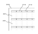
図1は、第一スリットを形成した基板の上面図である。また図2は、図1の斜視図である。図3は、第二スリットを形成した基板の上面図である。図4は、図3の斜視図である。図5は、基板を切断する図である。図6は、チップ部品(サブマウント)の斜視図である。図9は、スリット幅に対する主面側面膜厚比率を示す図である。 FIG. 1 is a top view of a substrate on which a first slit is formed. FIG. 2 is a perspective view of FIG. FIG. 3 is a top view of the substrate on which the second slit is formed. FIG. 4 is a perspective view of FIG. FIG. 5 is a diagram for cutting the substrate. FIG. 6 is a perspective view of a chip component (submount). FIG. 9 is a diagram showing the main-surface side film thickness ratio with respect to the slit width.
シリコンからなる厚さ200μm程度の基板200に、フォトリソグラフィーによりレジストパターンを形成し、DRIEにより第一スリット211を形成する。第一スリット211の幅は、DRIEの特性上、垂直性を向上させるためにはできるだけ狭い方が良い。しかしながら狭すぎるとフォトリソグラフィーによりレジストの最小開口幅の制限があることから、10〜20μm程度の幅が望ましい。
A resist pattern is formed by photolithography on a
図1および図2に示すように、環状に形成された第一スリット211により、基板200に島207が形成され、サブマウント201の少なくとも1つの側面が、エッチング面205として形成される。尚、基板200の下面をドライフィルム(不図示)により保持し、第一スリット211が基板200を貫通しても、基板200や島207の状態を保持できるようにしている。本実施例では、第一スリット211を一つのサブマウント201の側面に対応して形成しているが、必ずしもこれに限定するものではなく、複数のサブマウントの側面に対応して形成しても良い。
As shown in FIGS. 1 and 2, an
第一スリット211を形成した基板200を、レジスト剥離液に浸漬することによりDRIEのマスクとして用いたレジストや、基板200を保持しているドライフィルムを、基板200より剥離除去する。その時、島207も離脱させ、図3および図4に示すように、第一スリット211を含む第二スリット212が形成された基板200となる。
The
図6に示すように、サブマウント201は、エッチング面205を基準面として用い、はんだ溶着するため、エッチング面205にはある程度の金属膜、例えば下層よりTi/Pt/Auを成膜しておく必要がある。Tiはシリコンとの密着層、PtはAuがシリコンへの拡散防止、AuはAuSnはんだとの接合性保持の役割である。従って、エッチング面205への成膜を効率的に行うため、第二スリット212の幅は広くする必要がある。第一スリット211を形成した後、島207を除去することで、エッチング面205の垂直性を確保しつつ、成膜可能な開口を備えた第二スリット212を容易に形成することができる。
As shown in FIG. 6, since the
第二スリット212を形成した基板200に、スパッタリングにより金属膜を成膜した後、フォトリソグラフィーによりレジスト開口し、イオンミリングにより金属膜をエッチングし、サブマウント201の上面204および側面(エッチング面)205に、所定の回路パターン202を形成する。また、予め成膜したい部分をレジストにより開口し、スパッタリングにより成膜し、リフトオフ法により形成しても良い。
After a metal film is formed by sputtering on the
尚、基板200に金属膜または所定の回路パターン202を形成する際、後にダイシングブレード(不図示)を用いて、サブマウント201の個片化を行う切断領域には、ストリートと呼ばれる切断時にダイシングブレードと金属膜が接触しない金属膜開口部を設けるのが望ましい。
In addition, when forming a metal film or a predetermined
スパッタリング装置を用い、第二スリット212の幅を変えて、上面側より金属膜を成膜した際の側面(エッチング面)205の膜厚値のデータを図9に示す。下層よりTi/Pt/Auを成膜し、その合計とし、上面204の膜厚を100%とした場合の側面(エッチング面)205の膜厚比率を示したものである。この結果より第二スリット212の幅が400μm以上においては金属膜の入り込み量の変化がないことがわかる。
FIG. 9 shows data of film thickness values of the side surface (etching surface) 205 when a metal film is formed from the upper surface side by changing the width of the
次に、サブマウント201の上面204にフォトリソグラフィーによりレジストを開口し、レーザーダイオードを搭載するためのAuSnのはんだ膜203を形成する。
Next, a resist is opened on the
最後に、図5に示すように、基板200をダイシングブレードで切断し、切断溝214を形成することで、DRIEで形成された側面(エッチング面)205以外の切断面206を備えた個片のチップ部品(サブマウント)201が得られる。
Finally, as shown in FIG. 5, the
本実施例では、サブマウントを例に説明したが、これに限定するものではなく、チップ部品として、半導体基板に立体的に絶縁膜を形成する形態においても、同様に適用できる。 In this embodiment, the submount has been described as an example. However, the present invention is not limited to this, and the present invention can be similarly applied to a form in which an insulating film is three-dimensionally formed on a semiconductor substrate as a chip component.
100 基板
101 チップ部品
102 金属膜
103 電極
104 上面
106 切断面(側面)
113 ダイシングブレード
114 切断溝
200 基板
201 チップ部品(サブマウント)
202 回路パターン
203 はんだ膜
204 上面
205 エッチング面(側面)
206 切断面(側面)
207 島
211 第一スリット
212 第二スリット
214 切断溝
DESCRIPTION OF
113
202
206 Cut surface (side)
Claims (1)
前記基板の表面にレジストパターンを形成するレジストパターン形成工程と、
前記レジストパターンをマスクとして、前記基板をエッチングし、前記基板を貫通し、かつ、環状に形成され、前記チップ部品の少なくとも1つの側面を含む第一スリットを形成する第一スリット形成工程と、
環状に形成された前記第一のスリットに囲まれた部位を前記基板より取り除くことで、前記第一スリットを含む第二スリットを形成する第二スリット形成工程と、
前記第二スリット形成工程の後、前記チップ部品の少なくとも1つの前記側面に膜付けを行う膜形成工程と、
前記膜形成工程の後、前記基板を切断することで、前記チップ部品の他の側面を形成し、かつ、個片化する個片化工程と、
を有することを特徴とするチップ部品製造方法。
In a chip component manufacturing method in which a substrate is separated into pieces to form a plurality of chip components,
A resist pattern forming step of forming a resist pattern on the surface of the substrate;
Etching the substrate using the resist pattern as a mask, penetrating the substrate, and forming a first slit that is annularly formed and includes at least one side surface of the chip component;
A second slit forming step of forming a second slit including the first slit by removing a portion surrounded by the first slit formed in an annular shape from the substrate ;
After the second slit forming step, a film forming step of forming a film on at least one side surface of the chip component;
After the film formation step, by cutting the substrate, to form the other side surface of the chip component, and to singulation,
A method of manufacturing a chip part, comprising:
Priority Applications (1)
| Application Number | Priority Date | Filing Date | Title |
|---|---|---|---|
| JP2014240698A JP6382084B2 (en) | 2014-11-28 | 2014-11-28 | Chip parts manufacturing method |
Applications Claiming Priority (1)
| Application Number | Priority Date | Filing Date | Title |
|---|---|---|---|
| JP2014240698A JP6382084B2 (en) | 2014-11-28 | 2014-11-28 | Chip parts manufacturing method |
Publications (2)
| Publication Number | Publication Date |
|---|---|
| JP2016103551A JP2016103551A (en) | 2016-06-02 |
| JP6382084B2 true JP6382084B2 (en) | 2018-08-29 |
Family
ID=56089167
Family Applications (1)
| Application Number | Title | Priority Date | Filing Date |
|---|---|---|---|
| JP2014240698A Active JP6382084B2 (en) | 2014-11-28 | 2014-11-28 | Chip parts manufacturing method |
Country Status (1)
| Country | Link |
|---|---|
| JP (1) | JP6382084B2 (en) |
Family Cites Families (3)
| Publication number | Priority date | Publication date | Assignee | Title |
|---|---|---|---|---|
| JP2899542B2 (en) * | 1995-06-01 | 1999-06-02 | ホーヤ株式会社 | Method of manufacturing transfer mask |
| JPH10117043A (en) * | 1996-10-09 | 1998-05-06 | Toshiba Corp | Light emitting element |
| JP4219677B2 (en) * | 2002-12-26 | 2009-02-04 | 株式会社リコー | Manufacturing method of optical device |
-
2014
- 2014-11-28 JP JP2014240698A patent/JP6382084B2/en active Active
Also Published As
| Publication number | Publication date |
|---|---|
| JP2016103551A (en) | 2016-06-02 |
Similar Documents
| Publication | Publication Date | Title |
|---|---|---|
| US9589812B2 (en) | Fabrication method of semiconductor piece | |
| JP5637331B1 (en) | Semiconductor piece manufacturing method, circuit board including semiconductor piece, and image forming apparatus | |
| JP6441025B2 (en) | Manufacturing method of semiconductor chip | |
| US9735056B2 (en) | Semiconductor piece manufacturing method and substrate dicing method for suppressing breakage | |
| CN102254868B (en) | It is provided with the manufacture method of the chip component of distribution slot | |
| JP6462747B2 (en) | Semiconductor chip and semiconductor device | |
| JP6576735B2 (en) | Wafer division method | |
| JP5780351B1 (en) | Manufacturing method of semiconductor piece | |
| JP6382084B2 (en) | Chip parts manufacturing method | |
| US20170148697A1 (en) | Semiconductor device and method of making a semiconductor device | |
| CN105580145B (en) | Opto-electronic semiconductor chip, semiconductor devices and the method for manufacturing opto-electronic semiconductor chip | |
| JP6336895B2 (en) | Substrate and substrate manufacturing method | |
| CN103503175B (en) | Device carrier composite structure with trench structure separating device carrier regions and method for manufacturing multiple device carrier regions | |
| JP6478877B2 (en) | High-precision submount substrate and manufacturing method thereof | |
| JP2017034080A (en) | Semiconductor light-emitting element | |
| JP2016046461A (en) | Semiconductor light-emitting element wafer, semiconductor light-emitting element and manufacturing method of semiconductor light-emitting element | |
| CN105431252A (en) | Method for dividing a composite into semiconductor chips, and semiconductor chip | |
| JP2009130324A (en) | Method of manufacturing semiconductor device and the semiconductor device | |
| JP6504978B2 (en) | Submount manufacturing method | |
| JP6402549B2 (en) | Semiconductor laser device, manufacturing method thereof, and manufacturing method of semiconductor laser device | |
| US20200168505A1 (en) | Semiconductor Chip, Method of Producing a Semiconductor Chip and Apparatus Having a Plurality of Semiconductor Chips | |
| CN102142464A (en) | Surface mount diode and method of fabricating the same | |
| TWI625993B (en) | Manufacturing method of circuit board structure | |
| JP2013191810A (en) | Method for manufacturing semiconductor light-emitting element and semiconductor light-emitting element | |
| KR20210044394A (en) | Method of dicing power semiconductor |
Legal Events
| Date | Code | Title | Description |
|---|---|---|---|
| A621 | Written request for application examination |
Free format text: JAPANESE INTERMEDIATE CODE: A621 Effective date: 20170522 |
|
| A977 | Report on retrieval |
Free format text: JAPANESE INTERMEDIATE CODE: A971007 Effective date: 20180221 |
|
| A131 | Notification of reasons for refusal |
Free format text: JAPANESE INTERMEDIATE CODE: A131 Effective date: 20180228 |
|
| A521 | Written amendment |
Free format text: JAPANESE INTERMEDIATE CODE: A523 Effective date: 20180417 |
|
| TRDD | Decision of grant or rejection written | ||
| A01 | Written decision to grant a patent or to grant a registration (utility model) |
Free format text: JAPANESE INTERMEDIATE CODE: A01 Effective date: 20180730 |
|
| A61 | First payment of annual fees (during grant procedure) |
Free format text: JAPANESE INTERMEDIATE CODE: A61 Effective date: 20180801 |
|
| R150 | Certificate of patent or registration of utility model |
Ref document number: 6382084 Country of ref document: JP Free format text: JAPANESE INTERMEDIATE CODE: R150 |