JP6332734B2 - Liquid crystal display - Google Patents
Liquid crystal display Download PDFInfo
- Publication number
- JP6332734B2 JP6332734B2 JP2014029068A JP2014029068A JP6332734B2 JP 6332734 B2 JP6332734 B2 JP 6332734B2 JP 2014029068 A JP2014029068 A JP 2014029068A JP 2014029068 A JP2014029068 A JP 2014029068A JP 6332734 B2 JP6332734 B2 JP 6332734B2
- Authority
- JP
- Japan
- Prior art keywords
- liquid crystal
- strip
- display device
- pixel electrode
- crystal display
- Prior art date
- Legal status (The legal status is an assumption and is not a legal conclusion. Google has not performed a legal analysis and makes no representation as to the accuracy of the status listed.)
- Active
Links
- 239000004973 liquid crystal related substance Substances 0.000 title claims description 213
- 230000005684 electric field Effects 0.000 claims description 105
- 239000000758 substrate Substances 0.000 claims description 55
- 239000011159 matrix material Substances 0.000 claims description 12
- 239000010410 layer Substances 0.000 description 65
- 239000010408 film Substances 0.000 description 44
- 229910052751 metal Inorganic materials 0.000 description 17
- 239000002184 metal Substances 0.000 description 17
- 239000004065 semiconductor Substances 0.000 description 11
- 239000010409 thin film Substances 0.000 description 11
- 230000007423 decrease Effects 0.000 description 10
- 238000000034 method Methods 0.000 description 9
- 238000002834 transmittance Methods 0.000 description 9
- 238000002161 passivation Methods 0.000 description 7
- 238000005452 bending Methods 0.000 description 5
- 238000005530 etching Methods 0.000 description 5
- 229910001182 Mo alloy Inorganic materials 0.000 description 4
- 229910052581 Si3N4 Inorganic materials 0.000 description 4
- 230000000694 effects Effects 0.000 description 4
- AMGQUBHHOARCQH-UHFFFAOYSA-N indium;oxotin Chemical compound [In].[Sn]=O AMGQUBHHOARCQH-UHFFFAOYSA-N 0.000 description 4
- HQVNEWCFYHHQES-UHFFFAOYSA-N silicon nitride Chemical compound N12[Si]34N5[Si]62N3[Si]51N64 HQVNEWCFYHHQES-UHFFFAOYSA-N 0.000 description 4
- 229910021417 amorphous silicon Inorganic materials 0.000 description 3
- 230000005540 biological transmission Effects 0.000 description 2
- 210000002858 crystal cell Anatomy 0.000 description 2
- 230000007547 defect Effects 0.000 description 2
- 239000011229 interlayer Substances 0.000 description 2
- 238000004519 manufacturing process Methods 0.000 description 2
- 230000010287 polarization Effects 0.000 description 2
- 238000005728 strengthening Methods 0.000 description 2
- 229910000838 Al alloy Inorganic materials 0.000 description 1
- VYPSYNLAJGMNEJ-UHFFFAOYSA-N Silicium dioxide Chemical compound O=[Si]=O VYPSYNLAJGMNEJ-UHFFFAOYSA-N 0.000 description 1
- 238000013459 approach Methods 0.000 description 1
- 230000015572 biosynthetic process Effects 0.000 description 1
- 239000003990 capacitor Substances 0.000 description 1
- 230000015556 catabolic process Effects 0.000 description 1
- 210000004027 cell Anatomy 0.000 description 1
- 238000005229 chemical vapour deposition Methods 0.000 description 1
- 230000003247 decreasing effect Effects 0.000 description 1
- 230000002950 deficient Effects 0.000 description 1
- 238000006731 degradation reaction Methods 0.000 description 1
- 238000000151 deposition Methods 0.000 description 1
- 230000006866 deterioration Effects 0.000 description 1
- 238000005755 formation reaction Methods 0.000 description 1
- 239000011521 glass Substances 0.000 description 1
- 238000002347 injection Methods 0.000 description 1
- 239000007924 injection Substances 0.000 description 1
- 239000007788 liquid Substances 0.000 description 1
- 238000000059 patterning Methods 0.000 description 1
- 230000002093 peripheral effect Effects 0.000 description 1
- 238000003825 pressing Methods 0.000 description 1
- 238000007789 sealing Methods 0.000 description 1
- 229910052710 silicon Inorganic materials 0.000 description 1
- 229910052814 silicon oxide Inorganic materials 0.000 description 1
- 125000006850 spacer group Chemical group 0.000 description 1
- 238000004544 sputter deposition Methods 0.000 description 1
- 238000003860 storage Methods 0.000 description 1
Images


Classifications
-
- G—PHYSICS
- G02—OPTICS
- G02F—OPTICAL DEVICES OR ARRANGEMENTS FOR THE CONTROL OF LIGHT BY MODIFICATION OF THE OPTICAL PROPERTIES OF THE MEDIA OF THE ELEMENTS INVOLVED THEREIN; NON-LINEAR OPTICS; FREQUENCY-CHANGING OF LIGHT; OPTICAL LOGIC ELEMENTS; OPTICAL ANALOGUE/DIGITAL CONVERTERS
- G02F1/00—Devices or arrangements for the control of the intensity, colour, phase, polarisation or direction of light arriving from an independent light source, e.g. switching, gating or modulating; Non-linear optics
- G02F1/01—Devices or arrangements for the control of the intensity, colour, phase, polarisation or direction of light arriving from an independent light source, e.g. switching, gating or modulating; Non-linear optics for the control of the intensity, phase, polarisation or colour
- G02F1/13—Devices or arrangements for the control of the intensity, colour, phase, polarisation or direction of light arriving from an independent light source, e.g. switching, gating or modulating; Non-linear optics for the control of the intensity, phase, polarisation or colour based on liquid crystals, e.g. single liquid crystal display cells
- G02F1/133—Constructional arrangements; Operation of liquid crystal cells; Circuit arrangements
- G02F1/1333—Constructional arrangements; Manufacturing methods
- G02F1/1343—Electrodes
- G02F1/134309—Electrodes characterised by their geometrical arrangement
- G02F1/134363—Electrodes characterised by their geometrical arrangement for applying an electric field parallel to the substrate, i.e. in-plane switching [IPS]
-
- G—PHYSICS
- G02—OPTICS
- G02F—OPTICAL DEVICES OR ARRANGEMENTS FOR THE CONTROL OF LIGHT BY MODIFICATION OF THE OPTICAL PROPERTIES OF THE MEDIA OF THE ELEMENTS INVOLVED THEREIN; NON-LINEAR OPTICS; FREQUENCY-CHANGING OF LIGHT; OPTICAL LOGIC ELEMENTS; OPTICAL ANALOGUE/DIGITAL CONVERTERS
- G02F1/00—Devices or arrangements for the control of the intensity, colour, phase, polarisation or direction of light arriving from an independent light source, e.g. switching, gating or modulating; Non-linear optics
- G02F1/01—Devices or arrangements for the control of the intensity, colour, phase, polarisation or direction of light arriving from an independent light source, e.g. switching, gating or modulating; Non-linear optics for the control of the intensity, phase, polarisation or colour
- G02F1/13—Devices or arrangements for the control of the intensity, colour, phase, polarisation or direction of light arriving from an independent light source, e.g. switching, gating or modulating; Non-linear optics for the control of the intensity, phase, polarisation or colour based on liquid crystals, e.g. single liquid crystal display cells
- G02F1/133—Constructional arrangements; Operation of liquid crystal cells; Circuit arrangements
- G02F1/1333—Constructional arrangements; Manufacturing methods
- G02F1/1337—Surface-induced orientation of the liquid crystal molecules, e.g. by alignment layers
-
- G—PHYSICS
- G02—OPTICS
- G02F—OPTICAL DEVICES OR ARRANGEMENTS FOR THE CONTROL OF LIGHT BY MODIFICATION OF THE OPTICAL PROPERTIES OF THE MEDIA OF THE ELEMENTS INVOLVED THEREIN; NON-LINEAR OPTICS; FREQUENCY-CHANGING OF LIGHT; OPTICAL LOGIC ELEMENTS; OPTICAL ANALOGUE/DIGITAL CONVERTERS
- G02F1/00—Devices or arrangements for the control of the intensity, colour, phase, polarisation or direction of light arriving from an independent light source, e.g. switching, gating or modulating; Non-linear optics
- G02F1/01—Devices or arrangements for the control of the intensity, colour, phase, polarisation or direction of light arriving from an independent light source, e.g. switching, gating or modulating; Non-linear optics for the control of the intensity, phase, polarisation or colour
- G02F1/13—Devices or arrangements for the control of the intensity, colour, phase, polarisation or direction of light arriving from an independent light source, e.g. switching, gating or modulating; Non-linear optics for the control of the intensity, phase, polarisation or colour based on liquid crystals, e.g. single liquid crystal display cells
- G02F1/133—Constructional arrangements; Operation of liquid crystal cells; Circuit arrangements
- G02F1/1333—Constructional arrangements; Manufacturing methods
- G02F1/1343—Electrodes
- G02F1/13439—Electrodes characterised by their electrical, optical, physical properties; materials therefor; method of making
-
- G—PHYSICS
- G02—OPTICS
- G02F—OPTICAL DEVICES OR ARRANGEMENTS FOR THE CONTROL OF LIGHT BY MODIFICATION OF THE OPTICAL PROPERTIES OF THE MEDIA OF THE ELEMENTS INVOLVED THEREIN; NON-LINEAR OPTICS; FREQUENCY-CHANGING OF LIGHT; OPTICAL LOGIC ELEMENTS; OPTICAL ANALOGUE/DIGITAL CONVERTERS
- G02F1/00—Devices or arrangements for the control of the intensity, colour, phase, polarisation or direction of light arriving from an independent light source, e.g. switching, gating or modulating; Non-linear optics
- G02F1/01—Devices or arrangements for the control of the intensity, colour, phase, polarisation or direction of light arriving from an independent light source, e.g. switching, gating or modulating; Non-linear optics for the control of the intensity, phase, polarisation or colour
- G02F1/13—Devices or arrangements for the control of the intensity, colour, phase, polarisation or direction of light arriving from an independent light source, e.g. switching, gating or modulating; Non-linear optics for the control of the intensity, phase, polarisation or colour based on liquid crystals, e.g. single liquid crystal display cells
- G02F1/137—Devices or arrangements for the control of the intensity, colour, phase, polarisation or direction of light arriving from an independent light source, e.g. switching, gating or modulating; Non-linear optics for the control of the intensity, phase, polarisation or colour based on liquid crystals, e.g. single liquid crystal display cells characterised by the electro-optical or magneto-optical effect, e.g. field-induced phase transition, orientation effect, guest-host interaction or dynamic scattering
-
- G—PHYSICS
- G02—OPTICS
- G02F—OPTICAL DEVICES OR ARRANGEMENTS FOR THE CONTROL OF LIGHT BY MODIFICATION OF THE OPTICAL PROPERTIES OF THE MEDIA OF THE ELEMENTS INVOLVED THEREIN; NON-LINEAR OPTICS; FREQUENCY-CHANGING OF LIGHT; OPTICAL LOGIC ELEMENTS; OPTICAL ANALOGUE/DIGITAL CONVERTERS
- G02F1/00—Devices or arrangements for the control of the intensity, colour, phase, polarisation or direction of light arriving from an independent light source, e.g. switching, gating or modulating; Non-linear optics
- G02F1/01—Devices or arrangements for the control of the intensity, colour, phase, polarisation or direction of light arriving from an independent light source, e.g. switching, gating or modulating; Non-linear optics for the control of the intensity, phase, polarisation or colour
- G02F1/13—Devices or arrangements for the control of the intensity, colour, phase, polarisation or direction of light arriving from an independent light source, e.g. switching, gating or modulating; Non-linear optics for the control of the intensity, phase, polarisation or colour based on liquid crystals, e.g. single liquid crystal display cells
- G02F1/133—Constructional arrangements; Operation of liquid crystal cells; Circuit arrangements
- G02F1/1333—Constructional arrangements; Manufacturing methods
- G02F1/1337—Surface-induced orientation of the liquid crystal molecules, e.g. by alignment layers
- G02F1/133707—Structures for producing distorted electric fields, e.g. bumps, protrusions, recesses, slits in pixel electrodes
-
- G—PHYSICS
- G02—OPTICS
- G02F—OPTICAL DEVICES OR ARRANGEMENTS FOR THE CONTROL OF LIGHT BY MODIFICATION OF THE OPTICAL PROPERTIES OF THE MEDIA OF THE ELEMENTS INVOLVED THEREIN; NON-LINEAR OPTICS; FREQUENCY-CHANGING OF LIGHT; OPTICAL LOGIC ELEMENTS; OPTICAL ANALOGUE/DIGITAL CONVERTERS
- G02F1/00—Devices or arrangements for the control of the intensity, colour, phase, polarisation or direction of light arriving from an independent light source, e.g. switching, gating or modulating; Non-linear optics
- G02F1/01—Devices or arrangements for the control of the intensity, colour, phase, polarisation or direction of light arriving from an independent light source, e.g. switching, gating or modulating; Non-linear optics for the control of the intensity, phase, polarisation or colour
- G02F1/13—Devices or arrangements for the control of the intensity, colour, phase, polarisation or direction of light arriving from an independent light source, e.g. switching, gating or modulating; Non-linear optics for the control of the intensity, phase, polarisation or colour based on liquid crystals, e.g. single liquid crystal display cells
- G02F1/133—Constructional arrangements; Operation of liquid crystal cells; Circuit arrangements
- G02F1/1333—Constructional arrangements; Manufacturing methods
- G02F1/1343—Electrodes
- G02F1/134309—Electrodes characterised by their geometrical arrangement
- G02F1/134318—Electrodes characterised by their geometrical arrangement having a patterned common electrode
-
- G—PHYSICS
- G02—OPTICS
- G02F—OPTICAL DEVICES OR ARRANGEMENTS FOR THE CONTROL OF LIGHT BY MODIFICATION OF THE OPTICAL PROPERTIES OF THE MEDIA OF THE ELEMENTS INVOLVED THEREIN; NON-LINEAR OPTICS; FREQUENCY-CHANGING OF LIGHT; OPTICAL LOGIC ELEMENTS; OPTICAL ANALOGUE/DIGITAL CONVERTERS
- G02F1/00—Devices or arrangements for the control of the intensity, colour, phase, polarisation or direction of light arriving from an independent light source, e.g. switching, gating or modulating; Non-linear optics
- G02F1/01—Devices or arrangements for the control of the intensity, colour, phase, polarisation or direction of light arriving from an independent light source, e.g. switching, gating or modulating; Non-linear optics for the control of the intensity, phase, polarisation or colour
- G02F1/13—Devices or arrangements for the control of the intensity, colour, phase, polarisation or direction of light arriving from an independent light source, e.g. switching, gating or modulating; Non-linear optics for the control of the intensity, phase, polarisation or colour based on liquid crystals, e.g. single liquid crystal display cells
- G02F1/137—Devices or arrangements for the control of the intensity, colour, phase, polarisation or direction of light arriving from an independent light source, e.g. switching, gating or modulating; Non-linear optics for the control of the intensity, phase, polarisation or colour based on liquid crystals, e.g. single liquid crystal display cells characterised by the electro-optical or magneto-optical effect, e.g. field-induced phase transition, orientation effect, guest-host interaction or dynamic scattering
- G02F1/13706—Devices or arrangements for the control of the intensity, colour, phase, polarisation or direction of light arriving from an independent light source, e.g. switching, gating or modulating; Non-linear optics for the control of the intensity, phase, polarisation or colour based on liquid crystals, e.g. single liquid crystal display cells characterised by the electro-optical or magneto-optical effect, e.g. field-induced phase transition, orientation effect, guest-host interaction or dynamic scattering the liquid crystal having positive dielectric anisotropy
-
- G—PHYSICS
- G02—OPTICS
- G02F—OPTICAL DEVICES OR ARRANGEMENTS FOR THE CONTROL OF LIGHT BY MODIFICATION OF THE OPTICAL PROPERTIES OF THE MEDIA OF THE ELEMENTS INVOLVED THEREIN; NON-LINEAR OPTICS; FREQUENCY-CHANGING OF LIGHT; OPTICAL LOGIC ELEMENTS; OPTICAL ANALOGUE/DIGITAL CONVERTERS
- G02F1/00—Devices or arrangements for the control of the intensity, colour, phase, polarisation or direction of light arriving from an independent light source, e.g. switching, gating or modulating; Non-linear optics
- G02F1/01—Devices or arrangements for the control of the intensity, colour, phase, polarisation or direction of light arriving from an independent light source, e.g. switching, gating or modulating; Non-linear optics for the control of the intensity, phase, polarisation or colour
- G02F1/13—Devices or arrangements for the control of the intensity, colour, phase, polarisation or direction of light arriving from an independent light source, e.g. switching, gating or modulating; Non-linear optics for the control of the intensity, phase, polarisation or colour based on liquid crystals, e.g. single liquid crystal display cells
- G02F1/137—Devices or arrangements for the control of the intensity, colour, phase, polarisation or direction of light arriving from an independent light source, e.g. switching, gating or modulating; Non-linear optics for the control of the intensity, phase, polarisation or colour based on liquid crystals, e.g. single liquid crystal display cells characterised by the electro-optical or magneto-optical effect, e.g. field-induced phase transition, orientation effect, guest-host interaction or dynamic scattering
- G02F1/13712—Devices or arrangements for the control of the intensity, colour, phase, polarisation or direction of light arriving from an independent light source, e.g. switching, gating or modulating; Non-linear optics for the control of the intensity, phase, polarisation or colour based on liquid crystals, e.g. single liquid crystal display cells characterised by the electro-optical or magneto-optical effect, e.g. field-induced phase transition, orientation effect, guest-host interaction or dynamic scattering the liquid crystal having negative dielectric anisotropy
Landscapes
- Physics & Mathematics (AREA)
- Nonlinear Science (AREA)
- Chemical & Material Sciences (AREA)
- Crystallography & Structural Chemistry (AREA)
- General Physics & Mathematics (AREA)
- Optics & Photonics (AREA)
- Mathematical Physics (AREA)
- Geometry (AREA)
- Liquid Crystal (AREA)
- Spectroscopy & Molecular Physics (AREA)
- Devices For Indicating Variable Information By Combining Individual Elements (AREA)
Description
本発明は、液晶表示装置に関し、特に、高開口で、高画質化の実現が可能な横電界方式のアクティブマトリクス型液晶表示装置に関する。 The present invention relates to a liquid crystal display device, and more particularly to a lateral electric field type active matrix liquid crystal display device that can realize high image quality with a high aperture.
近年、視野角特性に優れたIPS(In-plane Switching)方式に代表される横方向電界方式の液晶表示装置が、テレビやモニタなど比較的大きいものから、タブレットやスマートフォンなど携帯可能なものまで、多くの情報端末に広く適用されている。IPS方式は、基板に垂直な方向から見て、ストリップ状(短冊状)の2種類の電極(画素電極と共通電極)が間隔をおいて平行に配置され、ストリップ状の画素電極とストリップ状の共通電極の間に印加される電界により液晶分子を駆動する方式である。このIPS方式では、液晶分子の配列が視野角を変えても大きく変化するように見えないため、観察者から見て見る方向を変えても表示に大きな変化がないことが特徴である。 In recent years, liquid crystal display devices of the horizontal electric field method represented by the IPS (In-plane Switching) method, which has excellent viewing angle characteristics, from relatively large devices such as TVs and monitors to portable devices such as tablets and smartphones, It is widely applied to many information terminals. In the IPS system, two types of strip-shaped (strip-shaped) electrodes (pixel electrode and common electrode) are arranged in parallel with a distance as viewed from a direction perpendicular to the substrate, and the strip-shaped pixel electrode and strip-shaped electrode are arranged in parallel. In this method, liquid crystal molecules are driven by an electric field applied between common electrodes. This IPS method is characterized in that the arrangement of liquid crystal molecules does not appear to change greatly even when the viewing angle is changed, and therefore, there is no significant change in display even when the viewing direction is viewed from the observer.
このように視野角が広いことを特徴とするIPS方式であるが、さらに視野角表示特性を向上させる目的で、次のようなマルチドメイン構造を用いる事がある。すなわち、上記のストリップ状の2種類の電極のある部分では、液晶に印加する電界方向を、液晶の初期配向方向に対して+θ゜となるように配置し、そして上記のストリップ状の2種類の電極の別の部分では−θ゜となるように配置し、双方を接続することで画素内における電極を屈曲させる構造をとらせる。なお、ストリップ状の電極(ストリップ状の画素電極、ストリップ状の共通電極)は独立している必要はなく、対向するひとつのペアのエッジ部分が平行になっていれば、端部形状がストリップ状でなくとも、各々の端部が接続されていたとしても、また、ペアを構成しない部分の形状が異型であってもかまわないものとする。 Although the IPS system is characterized by such a wide viewing angle, the following multi-domain structure may be used for the purpose of further improving the viewing angle display characteristics. That is, in a portion of the two strip-shaped electrodes, the electric field applied to the liquid crystal is arranged to be + θ ° with respect to the initial alignment direction of the liquid crystal, and the two strip-shaped electrodes are arranged. In another part of the electrode, it is arranged so as to be −θ °, and both are connected to bend the electrode in the pixel. Note that the strip-shaped electrodes (strip-shaped pixel electrodes, strip-shaped common electrodes) do not need to be independent, and the end shape is strip-shaped if the edge portions of one pair facing each other are parallel. Even if each end is connected, the shape of the portion not constituting the pair may be different.
しかしながら、このマルチドメイン構造では、+θ゜の電極部と−θ゜の電極部を接続する部分で屈曲部が存在する。この屈曲部は、右回転変形する液晶部と左回転変形する液晶部のドメイン境界となるため、ディスクリネーションが発生することとなり透過率を落とす要因になる。 However, in this multi-domain structure, a bent portion exists at a portion connecting the + θ ° electrode portion and the −θ ° electrode portion. Since the bent portion serves as a domain boundary between the liquid crystal portion that is deformed to rotate clockwise and the liquid crystal portion that is deformed to rotate counterclockwise, disclination occurs and causes a decrease in transmittance.
液晶表示装置の画素は、一対の基板の一方の基板に複数の走査線と複数のデータ線が配置され、そのうちの、2本の走査線と2本のデータ線を境界とする領域で分割される。この画素のサイズが小さくなると一画素あたりに占める走査線およびデータ線の面積が大きくなり、その結果、開口率が低下する。図20は、走査線幅、データ線幅をそれぞれ10μm一定とし、ある画素サイズのとき、この配線面積以外の領域を開口部と見立てた開口率との関係を示したグラフである。この関係からわかるように、特に画素サイズが100μm以下になると顕著に開口率は低下し、上述したマルチドメイン構造の場合、屈曲部による相対的な透過率の低下が無視できなくなると言う問題が生じる。 A pixel of a liquid crystal display device includes a plurality of scanning lines and a plurality of data lines arranged on one substrate of a pair of substrates, and is divided by a region having two scanning lines and two data lines as a boundary. The When the pixel size is reduced, the area of the scanning line and the data line occupied per pixel is increased, and as a result, the aperture ratio is decreased. FIG. 20 is a graph showing the relationship between the scanning line width and the data line width, each 10 μm constant, and the aperture ratio in which a region other than the wiring area is regarded as an opening when a certain pixel size is used. As can be seen from this relationship, particularly when the pixel size is 100 μm or less, the aperture ratio is remarkably lowered, and in the case of the multi-domain structure described above, there arises a problem that the relative decrease in transmittance due to the bent portion cannot be ignored. .
この問題を回避するためには、画素を屈曲させないシングルドメインの構造を採用することが有利であるが、マルチドメイン構造で得られた優れた視野角特性が、シングルドメイン構造にすることで失われることになる。この問題を解決するにあたり、特許文献1の本文中の図32、図36や、特許文献2の本文中の図45、図46、図48には、画素を屈曲させずに画素内で液晶分子を2方向に回転させる構造が開示されている。
In order to avoid this problem, it is advantageous to adopt a single-domain structure that does not bend the pixels, but the excellent viewing angle characteristics obtained by the multi-domain structure are lost by using the single-domain structure. It will be. In solving this problem, FIG. 32 and FIG. 36 in the text of
本願の図21は、これら従来技術の代表例として、特許文献1の本文中の図32、図36で示されている画素構造をそれぞれ(a)、(b)として表している(説明を容易とするために、図の上下を反転している)。これらの構造では、共通電極101と画素電極102、あるいは共通電極101または画素電極102のいずれか一方の電極の端部の形状を斜め方向にも形成させ、画素端部に近づくにつれ一方の電極が他方の電極に徐々に近接し、その近接する領域で異なる2方向の電界103、104を発生させている。このため画素内では液晶分子の回転方向が2つ生じることになり、画素の屈曲のないマルチドメイン化が可能となると述べている。しかしながら、共通電極101と画素電極102、あるいは、共通電極101または画素電極102のいずれか一方の電極の端部の形状が斜め方向にも形成されるため、本来開口部として利用できた領域が減少する。従って、透過率の低下を招くことになる。
FIG. 21 of the present application represents the pixel structures shown in FIGS. 32 and 36 in the text of
また、特許文献2の本文中の図44、図47でも上述のように画素を屈曲させずに画素内で液晶分子を2方向に回転させる画素構造が開示されている。本願の図22は、これら従来技術の代表例として特許文献2の本文中の図44で示されている画素構造を表している(ここでの説明に不要な蓄積容量線等は省いている)。これらの構造でも、一方の電極が他方の電極に徐々に近接し、その近接する領域で異なる2方向の電界103、104を発生させている。このため画素内では液晶分子の回転方向が2つ生じることになり、画素の屈曲のないマルチドメイン化が可能となると述べている。しかしながら、この構造も上述の理由と同じ理由で透過率の低下を招くことになる。
44 and 47 in the text of
またさらに、この構造では、別の理由で透過率の低下を招く。その理由を本明細書の図23と図24を参照して説明する。図23は、図22中の破線で囲んだ領域を拡大表示させたものである。この構造は、共通電極101と画素電極102が異なる層で形成され、かつ、画素内で一部重なる領域を有するが、この重なる領域およびその近傍におけるある特定の領域では、意図する電界方向103、104とは異なる方向の電界114、115が生じることになる。この電界114、115は、いわゆるフリンジ電界と呼ばれるものである。このため、電界114、115の影響を受ける領域に存在する液晶分子は、意図した方向とは逆の方向の回転を起こすため、逆回転ドメイン117が生じる。この逆回転ドメイン117と順回転ドメイン118との境界ではディスクリネーション116が発生し、透過率の低下を招くことになる。
Furthermore, this structure causes a decrease in transmittance for another reason. The reason will be described with reference to FIGS. 23 and 24 of this specification. FIG. 23 is an enlarged view of the area surrounded by the broken line in FIG. In this structure, the
これら、ディスクリネーション116、逆回転ドメイン117、順回転ドメイン118の様子を本願の図24に示す。また、このような順回転ドメインの近傍に逆回転ドメインが存在すると、駆動中に表示画面に指押しなどの外力が一時的に加わった場合、その間、液晶の配向は乱され、外力が解放されると再び液晶は元の配向に戻ろうとするが、外力がかかる前の状態よりも順回転ドメインが小さくなり、逆にその分、逆回転ドメインが大きくなった状態で安定してしまう現象が生じやすくなる。したがって、外力がかかる前の表示状態と指押しの外力が加わった後の表示状態が異なることが起こり、その結果、指押し跡として認識される表示不具合が発生する。この現象は、著しく画質の低下を招くことになる。
The state of the
本発明は、上記問題点に鑑みてなされたものであって、その主たる目的は、画素サイズが小さくても、高開口で視野角特性に優れ、指押し跡が発生しないIPS方式の液晶表示装置を提供することにある。 The present invention has been made in view of the above problems, and its main object is to provide an IPS liquid crystal display device that has a high aperture, excellent viewing angle characteristics, and does not generate finger press marks even when the pixel size is small. Is to provide.
上記目的を達成するため、本願の第1の発明の液晶表示装置は、一対の基板と、前記一対の基板の間に挟持される液晶層と、前記一対の基板の一方の基板上に、複数の直線状の走査線と、前記走査線と交差する複数の直線状のデータ線と、前記走査線と前記データ線とでマトリクス状に形成される複数の画素と、を具備し、前記各画素には、ストリップ状画素電極が前記データ線または前記走査線に沿って少なくとも1本延在し、前記ストリップ状画素電極より前記液晶層に近い層で共通電極が前記走査線および前記データ線を少なくとも覆うように格子状に形成され、前記ストリップ状画素電極と、前記ストリップ状画素電極の延在方向と平行な前記共通電極との間で、前記基板面にほぼ平行な電界を前記液晶層に印加する横電界方式の液晶表示装置において、前記ストリップ状画素電極の一方の端部には、ストリップ部より幅広の第1の矩形状画素電極がT字状に接続され、前記第1の矩形状画素電極側の前記共通電極で形成される開口部のコーナー部分が、前記第1の矩形状画素電極と重畳することを特徴とする。また、第1の発明において、前記ストリップ状画素電極は1画素内に複数本配置される場合、各々の前記ストリップ状画素電極に接続される前記第1の矩形状画素電極は互いに接続され、前記ストリップ状画素電極間にさらにストリップ状共通電極が配置され、前記ストリップ状共通電極の両端部は前記格子状の共通電極と接続されていることを特徴とする。 In order to achieve the above object, a liquid crystal display device according to a first invention of the present application includes a plurality of substrates on a pair of substrates, a liquid crystal layer sandwiched between the pair of substrates, and one of the pair of substrates. A plurality of linear data lines intersecting the scanning lines, and a plurality of pixels formed in a matrix by the scanning lines and the data lines. Includes at least one strip pixel electrode extending along the data line or the scan line, and a common electrode in the layer closer to the liquid crystal layer than the strip pixel electrode includes at least the scan line and the data line. An electric field substantially parallel to the substrate surface is applied to the liquid crystal layer between the strip-shaped pixel electrode and the common electrode parallel to the extending direction of the strip-shaped pixel electrode. Horizontal electric field type liquid In the display device, a first rectangular pixel electrode wider than the strip portion is connected to one end of the strip-shaped pixel electrode in a T-shape, and the common electrode on the first rectangular pixel electrode side The corner portion of the opening formed in (1) overlaps with the first rectangular pixel electrode. In the first invention, when a plurality of the strip pixel electrodes are arranged in one pixel, the first rectangular pixel electrodes connected to the respective strip pixel electrodes are connected to each other, and A strip-shaped common electrode is further disposed between the strip-shaped pixel electrodes, and both ends of the strip-shaped common electrode are connected to the grid-shaped common electrode.
本願の第2の発明の液晶表示装置は、一対の基板と、前記一対の基板の間に挟持される液晶層と、前記一対の基板の一方の基板上に、複数の直線状の走査線と、前記走査線と交差する複数の直線状のデータ線と、前記走査線と前記データ線とでマトリクス状に形成される複数の画素と、を具備し、前記各画素には、ストリップ状画素電極が前記データ線または前記走査線に沿って少なくとも1本延在し、前記ストリップ状画素電極より前記液晶層に近い層で共通電極が前記走査線および前記データ線を少なくとも覆うように格子状に形成され、前記ストリップ状画素電極と、前記ストリップ状画素電極の延在方向と平行な前記共通電極との間で、前記基板面にほぼ平行な電界を前記液晶層に印加する横電界方式の液晶表示装置において、前記ストリップ状画素電極の一方の端部には、ストリップ部より幅広の突起状画素電極が前記共通電極で形成される開口部外で接続され、前記突起状画素電極側の前記開口部のコーナー部分が、前記突起状画素電極の両端の突起部と重畳することを特徴とする。また、第2の発明において、前記ストリップ状画素電極は1画素内に複数本配置される場合、各々の前記ストリップ状画素電極に接続される前記突起状画素電極は互いに接続され、前記ストリップ状画素電極間にさらにストリップ状共通電極が配置され、前記ストリップ状共通電極の両端部は前記格子状の共通電極と接続されていることを特徴とする。 A liquid crystal display device according to a second invention of the present application includes a pair of substrates, a liquid crystal layer sandwiched between the pair of substrates, and a plurality of linear scanning lines on one of the pair of substrates. A plurality of linear data lines intersecting the scanning lines, and a plurality of pixels formed in a matrix by the scanning lines and the data lines, and each pixel has a strip-like pixel electrode. Extends at least one along the data line or the scanning line, and a common electrode is formed in a lattice shape so as to cover at least the scanning line and the data line in a layer closer to the liquid crystal layer than the strip pixel electrode. A horizontal electric field type liquid crystal display in which an electric field substantially parallel to the substrate surface is applied to the liquid crystal layer between the strip pixel electrode and the common electrode parallel to the extending direction of the strip pixel electrode. In the apparatus, A projecting pixel electrode having a width wider than that of the strip portion is connected to one end of the trip-like pixel electrode outside the opening formed by the common electrode, and a corner portion of the opening on the projecting pixel electrode side is provided. , and wherein the overlapping with protrusions at both ends of the protruding pixel electrodes. In the second invention, when a plurality of the strip pixel electrodes are arranged in one pixel, the protruding pixel electrodes connected to the strip pixel electrodes are connected to each other, and the strip pixel A strip-shaped common electrode is further disposed between the electrodes, and both ends of the strip-shaped common electrode are connected to the grid-shaped common electrode.
また、本願の第1の発明及び第2の発明において、前記共通電極が前記画素内に向かって凸状を成している領域を有し、前記ストリップ状画素電極の他方の端部には、ストリップ部より幅広の第2の矩形状画素電極がT字状に接続され、前記領域が前記第2の矩形状画素電極と重畳することを特徴とする。 In the first and second inventions of the present application, the common electrode has a region that protrudes into the pixel, and the other end of the strip-shaped pixel electrode has A second rectangular pixel electrode having a width wider than that of the strip portion is connected in a T-shape, and the region overlaps with the second rectangular pixel electrode.
ここで、ストリップ状画素電極、第1の矩形状画素電極又は突起状画素電極、第2の矩形状画素電極、共通電極で囲われた領域をコラムと称すると、画素内にコラムは複数存在し、主にこのコラム内で液晶分子がツイスト変形を起こす。この際、複数のコラムは、それぞれツイスト変形方向が異なる二つの領域のどちらかに対応する。すなわち、以上のような画素構造を適用することにより、画素内における液晶のツイスト変形方向が異なるコラムが存在するために視野角特性に優れ、また高開口で指押し跡が発生しない横電界方式の液晶表示装置を得ることが可能となる。 Here, when a region surrounded by the strip-shaped pixel electrode, the first rectangular pixel electrode or the protruding pixel electrode, the second rectangular pixel electrode, and the common electrode is referred to as a column, there are a plurality of columns in the pixel. In this column, liquid crystal molecules cause twist deformation. At this time, each of the plurality of columns corresponds to one of two regions having different twist deformation directions. That is, by applying the pixel structure as described above, there is a column in which the twist deformation direction of the liquid crystal in the pixel is different, so that the viewing angle characteristics are excellent, and the lateral electric field method does not generate a finger press mark with a high aperture. A liquid crystal display device can be obtained.
なお、本願の第1の発明又は第2の発明では、共通電極を液晶層に近い側にすることにより、画素電極と共通電極との間の絶縁膜を、共通電極とデータ線との間の層間絶縁膜と共通にすることができ、その結果、絶縁膜の形成回数を少なくすることができるため、より低コストで形成することができる。 In the first invention or the second invention of the present application, the insulating film between the pixel electrode and the common electrode is provided between the common electrode and the data line by setting the common electrode closer to the liquid crystal layer. The interlayer insulating film can be used in common, and as a result, the number of insulating films can be reduced, so that it can be formed at a lower cost.
本願の第3の発明の液晶表示装置は、一対の基板と、前記一対の基板の間に挟持される液晶層と、前記一対の基板の一方の基板上に、複数の直線状の走査線と、
前記走査線と交差する複数の直線状のデータ線と、前記走査線と前記データ線でマトリクス状に形成される複数の画素と、を具備し、前記走査線および前記データ線を少なくとも覆うように共通電極が格子状に形成され、前記各画素には、前記共通電極よりも前記液晶層に近い層でストリップ状画素電極が前記データ線または前記走査線に沿って延在し、前記ストリップ状画素電極と、前記ストリップ状画素電極の延在方向と平行な前記共通電極との間で、前記基板面にほぼ平行な電界を前記液晶層に印加する横電界方式の液晶表示装置において、前記ストリップ状画素電極の一端には、ストリップ部より幅広の矩形状画素電極がT字状に接続され、前記矩形状画素電極が前記共通電極で形成される開口部に張り出さずに前記共通電極と重畳していることを特徴とする。
According to a third aspect of the present invention, there is provided a liquid crystal display device comprising: a pair of substrates; a liquid crystal layer sandwiched between the pair of substrates; and a plurality of linear scanning lines on one of the pair of substrates. ,
A plurality of linear data lines intersecting with the scanning lines, and a plurality of pixels formed in a matrix by the scanning lines and the data lines, so as to cover at least the scanning lines and the data lines. A common electrode is formed in a lattice shape, and in each pixel, a strip-like pixel electrode extends along the data line or the scanning line in a layer closer to the liquid crystal layer than the common electrode. In a horizontal electric field type liquid crystal display device in which an electric field substantially parallel to the substrate surface is applied to the liquid crystal layer between the electrode and the common electrode parallel to the extending direction of the strip pixel electrode, the strip shape At one end of the pixel electrode, a rectangular pixel electrode wider than the strip portion is connected in a T-shape, and the rectangular pixel electrode overlaps with the common electrode without overhanging the opening formed by the common electrode. And wherein the are.
本願の第3の発明では、画素電極を液晶層に近い側にすることにより、画素電極とデータ線との間に絶縁膜が形成される。このため、画素電極もしくはデータ線のパターン崩れに伴う画素電極とデータ線の短絡を防止することができる。 In the third invention of the present application, the insulating film is formed between the pixel electrode and the data line by setting the pixel electrode closer to the liquid crystal layer. For this reason, it is possible to prevent the pixel electrode and the data line from being short-circuited due to the pattern collapse of the pixel electrode or the data line.
本願の第1の発明乃至第3の発明において、前記液晶層の液晶分子の初期配向方位が、前記ストリップ状画素電極の延在方向と略一致することを特徴とする。 In any one of the first to third aspects of the present invention, the initial alignment direction of the liquid crystal molecules of the liquid crystal layer substantially coincides with the extending direction of the strip-shaped pixel electrode.
このとき、液晶分子の誘電率異方性は正のもの(以降、ポジ液晶と称する。また同様に誘電率異方性が負のものをネガ液晶と称する。)を適用する必要がある。ポジ液晶はネガ液晶に比べ、一般的に誘電率異方性が大きく粘度が低いため、低電圧駆動と高速応答が可能になる。 At this time, it is necessary to apply a liquid crystal molecule having a positive dielectric anisotropy (hereinafter referred to as a positive liquid crystal, and similarly having a negative dielectric anisotropy as a negative liquid crystal). A positive liquid crystal generally has a large dielectric anisotropy and a low viscosity as compared with a negative liquid crystal, so that a low voltage drive and a high-speed response are possible.
本願の第1の発明乃至第3の発明において、前記液晶層の液晶分子の初期配向方位が、前記ストリップ状画素電極の延在方向と垂直な方向と略一致することを特徴とする。 In the first to third inventions of the present application, the initial alignment direction of the liquid crystal molecules of the liquid crystal layer substantially coincides with a direction perpendicular to the extending direction of the strip-like pixel electrode.
このとき、ネガ液晶を適用する必要がある。ホモジニアス配向のネガ液晶は前記基板面に対し垂直な方向の成分を持った電界に対して変形を起こすことはほぼない。したがって、前記垂直な方向の成分を持った電界に対し前記ホモジニアス配向は変形を起こすことなく、基板面に平行な方向の成分をもった電界に対してツイスト変形を起こすため、視野角特性に優れた表示特性を得ることが可能になる。 At this time, it is necessary to apply a negative liquid crystal. The homogeneously aligned negative liquid crystal is hardly deformed by an electric field having a component in a direction perpendicular to the substrate surface. Therefore, the homogeneous orientation does not cause deformation with respect to the electric field having the component in the vertical direction, and causes twist deformation with respect to the electric field having the component in the direction parallel to the substrate surface. Display characteristics can be obtained.
本願の第1の発明乃至第3の発明において、前記画素電極、および前記共通電極はそれぞれ透明であることを特徴とする。 In the first to third inventions of the present application, the pixel electrode and the common electrode are each transparent.
透明の導電膜を適用することにより、各々の電極上の一部からの透過が起こるため、透過率の増加が実現できる。 By applying a transparent conductive film, transmission from a part of each electrode occurs, so that an increase in transmittance can be realized.
本発明によれば、画素サイズが小さくても、高開口で視野角特性に優れ、指押し跡が発生しないIPS方式の液晶表示装置を提供することが可能となる。 According to the present invention, even if the pixel size is small, it is possible to provide an IPS liquid crystal display device that has a high aperture, excellent viewing angle characteristics, and does not generate finger press marks.
背景技術で示したように、IPS方式の横電界液晶表示装置においては、画素のサイズが小さくなると、開口率の低下が生じる。これらの課題を解決するために、画素を屈曲させずに画素内で液晶分子を2方向に回転させる画素構造が提案されているが、従来の構造では、本来開口部として利用できた領域が電極で占められるために透過率の低下が起こり、またあるいは、液晶分子が意図した方向とは逆の方向に回転するため透過率の低下や指押し跡として認識される表示不具合が課題として残ってしまう。 As shown in the background art, in the IPS type horizontal electric field liquid crystal display device, when the pixel size is reduced, the aperture ratio is lowered. In order to solve these problems, a pixel structure in which liquid crystal molecules are rotated in two directions within a pixel without bending the pixel has been proposed. In the conventional structure, an area originally usable as an opening is an electrode. As a result, the transmittance decreases, or the liquid crystal molecules rotate in a direction opposite to the intended direction, which causes a decrease in transmittance and a display defect recognized as a finger press mark remains as a problem. .
そこで、本発明の一実施の形態では、各画素にデータ線または走査線に沿ってストリップ状画素電極を設け、ストリップ状画素電極より液晶層に近い層で走査線およびデータ線を少なくとも覆うように格子状の共通電極を設け、ストリップ状画素電極が複数本配置される場合は、ストリップ状画素電極間にさらにストリップ状共通電極を設け、ストリップ状共通電極の両端部は格子状の共通電極と接続し、ストリップ状画素電極の一方の端部に、ストリップ部より幅広の第1の矩形状画素電極をT字状に接続し、第1の矩形状画素電極側の共通電極で形成される開口部のコーナー部分が、第1の矩形状画素電極と重畳するようにしたり、ストリップ状画素電極の一方の端部に、ストリップ部より幅広の突起状画素電極を共通電極で形成される開口部外で接続し、突起状画素電極側の開口部のコーナー部分が、突起状画素電極の両端の突起部と重畳するようにしたりする。 Therefore, in one embodiment of the present invention, each pixel is provided with a strip-shaped pixel electrode along the data line or the scanning line, and at least the scanning line and the data line are covered with a layer closer to the liquid crystal layer than the strip-shaped pixel electrode. When a grid-like common electrode is provided and a plurality of strip-like pixel electrodes are arranged, a strip-like common electrode is further provided between the strip-like pixel electrodes, and both ends of the strip-like common electrode are connected to the grid-like common electrode. Then, a first rectangular pixel electrode wider than the strip portion is connected to one end of the strip-shaped pixel electrode in a T shape, and an opening formed by the common electrode on the first rectangular pixel electrode side The corner portion of the pixel electrode overlaps with the first rectangular pixel electrode, or a protruding pixel electrode wider than the strip portion is formed as a common electrode at one end portion of the strip pixel electrode. Connect mouth outer corner portion of the opening portion of the protruding pixel electrode side, or so as to overlap with the protruding portions at both ends of the protruding pixel electrodes.
また、走査線およびデータ線を少なくとも覆うように格子状の共通電極を設け、各画素に共通電極より液晶層に近い層で走査線またはデータ線に沿ってストリップ状画素電極を設け、ストリップ状画素電極が複数本配置される場合は、ストリップ状画素電極間にさらにストリップ状共通電極を設け、ストリップ状共通電極の両端部は格子状の共通電極と接続し、ストリップ状画素電極の一方の端部に、ストリップ部より幅広の矩形状画素電極をT字状に接続し、矩形状画素電極が共通電極で形成される開口部に張り出さずに共通電極と重畳するようにする。 Also, a grid-like common electrode is provided so as to cover at least the scanning line and the data line, and a strip-like pixel electrode is provided along each scanning line or data line in a layer closer to the liquid crystal layer than each common electrode. When a plurality of electrodes are arranged, a strip-shaped common electrode is further provided between the strip-shaped pixel electrodes, and both ends of the strip-shaped common electrode are connected to the grid-shaped common electrode, and one end of the strip-shaped pixel electrode In addition, a rectangular pixel electrode having a width wider than that of the strip portion is connected in a T shape so that the rectangular pixel electrode overlaps with the common electrode without overhanging the opening formed by the common electrode.
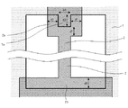
本発明の実施例1について、図1乃至図4を用いて説明する。図1は本発明の実施例1に係る液晶表示装置の1画素の構成を示す平面図である(単位画素を破線で示す)。図2は、図1に示すA−A’部の断面図であり、液晶層、対向基板も図示している。図3は、図1におけるコラムとその周辺を拡大した図である。図4は、図3における画素の上側部分と下側部分をそれぞれさらに拡大した図である。図1乃至図4に示す実施例1を、以下詳細に説明する。
A first embodiment of the present invention will be described with reference to FIGS. FIG. 1 is a plan view showing a configuration of one pixel of a liquid crystal display device according to
第一の透明絶縁性基板11に、隣接する2本の走査線6と隣接する2本のデータ線5を境界とする画素が形成され、この画素には、1本のストリップ状画素電極2と、走査線6およびデータ線5を覆う格子状の共通電極1が形成され、ストリップ状画素電極2とデータ線5を覆っている共通電極1が交互に配置されており、共通電極1は、ストリップ状画素電極2より液晶9に近い層に形成される。ストリップ状画素電極2は、画素の中央部にデータ線5の延在方向に沿って配置され、さらに、長手方向が、データ線5を覆っている共通電極1より短く、且つ、ストリップ状画素電極2の一端には、矩形状の画素電極(第1の矩形状画素電極2b)が設けられ、T字状に接続されている。つまり、ストリップ状画素電極2の一方の端部には、ストリップ部より幅広の第1の矩形状画素電極2bがT字状に略垂直の関係で接続され、さらにこの第1の矩形状画素電極2bは共通電極1で形成される開口部28の2つのコーナー部分と重畳することになる。また、ストリップ状画素電極2の長手方向の他端側には、走査線6を覆っている共通電極1から開口部28側にはみ出すように設けられた共通電極(凸状共通電極1a)を有し、且つ、そのはみ出すように設けられた凸状共通電極1aを覆うように設けられ、該凸状共通電極1aより大きい矩形状の画素電極(第2の矩形状画素電極2a)がストリップ状画素電極2の他端に接続されている。つまり、ストリップ状画素電極2の他方の端部には、ストリップ部より幅広の第2の矩形状画素電極2aがT字状に接続され、凸状共通電極1aと重畳することになる。このときの液晶配向方位7は、ストリップ状画素電極2が延在する方向にとっている。
On the first transparent insulating
ここで走査線6およびデータ線5を覆う共通電極1、凸状共通電極1a、ストリップ状画素電極2、第2の矩形状画素電極2a、第1の矩形状画素電極2bの詳細な位置関係について図3、図4を用いて述べる。図3は、図1の画素内のコラムとその周辺を拡大して示したものである。図4は、図3に示す画素の上側部分と下側部分をそれぞれさらに拡大して示したものである。
Here, the detailed positional relationship of the
まず、図3について述べる。このような構造をした横電界方式の液晶表示装置において、両電極間に電位差が生じたとき、横方向電界8が生じるが、これ以外にも、共通電極1と第2の矩形状画素電極2aおよび第1の矩形状画素電極2bが近接した領域での横方向電界21a、21bや、共通電極1および凸状共通電極1aと第2の矩形状画素電極2aおよび第1の矩形状画素電極2bから発せられるフリンジ電界22a、22bがある。本発明では、特にフリンジ電界22a、22bが重要となる。その理由として、液晶配向方位7は、横方向電界8の方向と垂直(90度)の関係にあり、この場合、初期配向状態にある液晶が、横方向電界8が生じたときにツイスト変形を起こそうとするが、図3で示す右側のコラムに存在する液晶は22aのフリンジ電界による変形開始のほうが早いためにフリンジ電界22aの影響が波及してiiの方向に変形する。左側のコラムに存在する液晶は同様にフリンジ電界22bに影響を受けiの方向に変形する。つまり、液晶配向方位7と横方向電界8の方向が垂直(90度)の関係でありながら、液晶のツイスト変形方向がストリップ状画素電極2と共通電極1から構成される2つのコラム各々で異なるようになる。
First, FIG. 3 will be described. In the horizontal electric field type liquid crystal display device having such a structure, when a potential difference is generated between both electrodes, a horizontal
補足すると、このときストリップ状画素電極2の右側のコラムに存在する液晶はiiの方向に変形するが、この方向と逆方向の横方向電界21aがコラム内に発生する。しかし、この横方向電界21aは、すぐ近傍にあるフリンジ電界22aと比較すると弱いために、横方向電界21aが働く領域に存在する液晶も、横方向電界21aの方向に変形を起こすことはなく、iiの方向に変形することになる。同様に、ストリップ状画素電極2の左側のコラムに存在する液晶はiの方向に変形するが、この方向と逆方向の横方向電界21bがコラム内に発生している。しかし、この横方向電界21bも、すぐ近傍にあるフリンジ電界22bと比較すると弱いために、横方向電界21bが働く領域に存在する液晶も、横方向電界21bの方向に変形を起こすことはなく、iの方向に変形することになる。また、厳密に言うと、本画素内で発生するフリンジ電界は、22a、22bの斜め方向以外にも、データ線5や走査線6が延在する方向にも存在するが、これらは液晶のツイスト変形方向には影響を与えないので、ここでは省略している。
Supplementally, at this time, the liquid crystal present in the column on the right side of the strip-shaped
次に、図4について述べる。図4には、凸状共通電極1aと第2の矩形状画素電極2a、第1の矩形状画素電極2bを示している。第2の矩形状画素電極2aが凸状共通電極1aから張り出す距離d1と第1の矩形状画素電極2bの共通電極1からの張り出す距離d2は、少なくとも0または0より大きければよいが、ここでは、2μmとした。また、凸状共通電極1aの突き出す距離d3は、2〜3μmあれば十分であるが、ここでは5μmとし、幅d4は、3μmとした。
Next, FIG. 4 will be described. FIG. 4 shows a convex
以上のような画素構造を適用することにより、画素内における液晶のツイスト変形方向が異なるコラムが複数存在するために、屈曲させたマルチドメイン構造と同じような優れた視野角特性が得られ、さらに、図21、図22で述べたように各電極の端部の形状が斜め方向に形成されないために開口領域の減少はなく、また、フリンジ電界22a、22bによって液晶ツイスト方向を制御しているので、指押し跡に強く、加えて高速応答も実現できるIPS方式の液晶表示装置を得ることが可能となる。
By applying the pixel structure as described above, there are a plurality of columns having different twist deformation directions of the liquid crystal in the pixel, so that excellent viewing angle characteristics similar to a bent multi-domain structure can be obtained. As shown in FIGS. 21 and 22, since the shape of the end portion of each electrode is not formed in an oblique direction, the opening area is not reduced, and the liquid crystal twist direction is controlled by the fringe
また、本実施例では、共通電極1が画素電極2より液晶層に近い。共通電極1を液晶層に近い側にすることにより、画素電極2と共通電極1との間の絶縁膜を、共通電極1とデータ線5との間の層間絶縁膜と共通にすることができ、その結果、絶縁膜の形成回数を少なくすることができるため、より低コストで形成することができる。
In this embodiment, the
以上が、実施例1に関する構造の詳細な説明となるが、以下に製造方法の一例についても述べる。 The above is a detailed description of the structure relating to the first embodiment. An example of the manufacturing method will be described below.
まず、第一の透明絶縁性基板11としてガラス基板上に、モリブデン合金からなる第一金属層をスパッタ法により、300nmの厚さで形成させ、走査線6のパターンに加工する。
First, a first metal layer made of a molybdenum alloy is formed on the glass substrate as the first transparent insulating
次に、ゲート絶縁膜12として、酸化シリコンを100nm堆積させた後、PCVD(Plasma Chemical Vapor Deposition)法により、窒化シリコンを300nm、i−a−Si(intrinsic amorphous Silicon)を170nm、n−a−Si(n-type amorphous Silicon)を30nm、それぞれ連続的に堆積させる。i−a−Siとn−a−Siとの積層膜は、薄膜半導体層4となる部分を残して、エッチング除去する。
Next, after depositing 100 nm of silicon oxide as the
次に、ITO(Indium Tin Oxide)等の透明導電膜により、画素電極2を走査線6の延在方向に垂直(90度)な方向に、ストリップ状に40nmの厚さで形成する。またこのとき同時に、第2の矩形状画素電極2a、第1の矩形状画素電極2bも形成する。
Next, the
次に、第二金属層として、モリブデン合金の膜を300nm形成させ、データ線5、ソース電極3のパターンに加工する。データ線5は、ストリップ状画素電極2、第2の矩形状画素電極2a、第1の矩形状画素電極2bと重ならないように、かつストリップ状画素電極2と平行に配置される。また、ソース電極3は、第1の矩形状画素電極2bと一部重なる領域を持ち、電気的に導通されるように配置される。なお、TFT(Thin Film Transistor)は、走査線6の一部、ゲート絶縁膜12、薄膜半導体層4、データ線5の一部、およびソース電極3から構成される。
Next, as a second metal layer, a molybdenum alloy film is formed to a thickness of 300 nm and processed into a pattern of the
次に、第二金属層をマスクとして、TFTの薄膜半導体層4の不要なn−a−Si層をエッチングによって除去する。
Next, an unnecessary na-Si layer of the thin
次に、パッシベーション膜13として、窒化シリコンを500nm堆積させる。
Next, 500 nm of silicon nitride is deposited as the
次に、表示画面周辺に引き出された走査線6およびデータ線5の端子部で金属層を露出させるために、ゲート絶縁膜12、およびパッシベーション膜13の必要部分をエッチング除去する。
Next, in order to expose the metal layer at the terminal portions of the
次に、ITO(Indium Tin Oxide)等の透明導電膜により、共通電極1を、走査線6およびデータ線5を覆うように厚さ80nmで形成する。またこのとき同時に、凸状共通電極1aも形成する。さらに共通電極1は、表示画面周辺部に第一の金属層および第二の金属層、またはいずれかの金属層によって形成された共通電極配線とコンタクトホールを介して導通されるが、図による説明は省略している。また、走査線6を覆うように配置されている共通電極1は、TFTのチャネル部の直上は形成させないようにパターン加工してもよい。
Next, the
上述のようにして形成したTFT側の基板に、配向膜14を塗布、焼成する。一方、対向基板となる第二の透明絶縁性基板19には、ブラックマトリクス18、カラーフィルタとなる色層17、オーバーコート16、および、TFT側基板と対向基板との間に空間を確保させるための柱状スペーサ(図中には示していない)を形成し、更にその上に配向膜15を塗布、焼成する。そして、両基板の配向膜14、15に対し走査線6の延在方向に垂直(90度)な方向にラビング処理をし、液晶配向方位7をとり、両基板を貼り合せて、周辺をシールで固めて、中に液晶9を注入し、封孔する。液晶セルギャップは3.5μmになるようにし、屈折率異方性Δn=0.09、誘電率異方性Δε=10の液晶9(ポジ液晶)を用いる。液晶9の注入に際しては、十分に液晶9がセル内に入るように、注入時間を十分とって実施する。また、液晶セル内が所定の圧力となるように、加圧を行いながら、封孔を実施する。当然ながら、液晶滴下工法によって、両基板のラビング処理後に液晶9の充填、両基板の貼り合せ、周辺のシール固めの工程を行なうことも可能である。
The
上述のようにして作製した液晶表示パネルのTFT側基板に、偏光軸が液晶のラビング方向となる液晶配向方位7に一致する偏光板10を貼り付け、対向基板にはクロスニコルとなるように偏光板20を貼り付ける。
A
更に、周辺に必要な駆動ドライバを実装し、バックライト及び信号処理基板をしかるべき形に組み立てて、アクティブマトリクス型液晶表示装置を作製する。 Further, necessary driver drivers are mounted on the periphery, and the backlight and the signal processing board are assembled into appropriate shapes to produce an active matrix liquid crystal display device.
この液晶表示装置は、IPS(In-Plane Switching)モードであり、ラビング方向にホモジニアス配向させた液晶を、データ線5に沿った共通電極1とストリップ状画素電極2の間に形成される基板に略平行な横方向電界8により、面内にツイスト変形させることで、画素ごとの透過光量を制御する。
This liquid crystal display device is in an IPS (In-Plane Switching) mode, and a liquid crystal that is homogeneously aligned in the rubbing direction is formed on a substrate formed between the
本実施例1では、解像度が横1024×RGB本、縦768本のXGAを適用した。画素サイズを69μmとし、データ線幅3μm、データ線上の共通電極幅9μm、画素電極幅3μmとした。この場合、ストリップ状画素電極2とデータ線5に沿った共通電極1の間隔は5.5μmとなる。
In the first embodiment, an XGA having a resolution of 1024 × RGB and 768 vertical is applied. The pixel size was 69 μm, the data line width was 3 μm, the common electrode width on the data line was 9 μm, and the pixel electrode width was 3 μm. In this case, the distance between the strip-shaped
上述したこれらの設定値は、本実施例1で適用している設定値であり、特に限定されるものではなく、適宜設定されるべき値である。例えば、本実施例1では、金属層にモリブデン合金を使用しているが、特にこれに限定されず、アルミニウム合金なども用いてよい。また、本実施例1では、薄膜半導体層4を形成後に、透明導電膜による画素電極2、ソース電極3およびデータ線5の形成、薄膜半導体層4の不要なn−a−Si層のエッチングの工程順で作製しているが、これに限定されず、例えば、薄膜半導体層4を形成後、ソース電極3およびデータ線5の形成、薄膜半導体層4の不要なn−a−Si層のエッチング、透明導電膜による画素電極2の形成、という工程順で作製してもよい。
These setting values described above are the setting values applied in the first embodiment, are not particularly limited, and are values that should be set as appropriate. For example, in the first embodiment, a molybdenum alloy is used for the metal layer, but the present invention is not particularly limited thereto, and an aluminum alloy or the like may be used. In the first embodiment, after the thin
本発明の実施例2について、図5、図6、図7を用いて説明する。図5は本発明の実施例2に係る液晶表示装置の1画素の構成を示す平面図である(単位画素を破線で示す)。図6は、図5に示すB−B’部の断面図であり、液晶層、対向基板も図示している。図7は、図6の画素内のコラムとその周辺を拡大して示したものである。図5、図6、図7に示す実施例2を、以下詳細に説明する。
A second embodiment of the present invention will be described with reference to FIGS. FIG. 5 is a plan view showing the configuration of one pixel of a liquid crystal display device according to
実施例1では、図1等で示すように、画素電極に透明導電膜を用いたが、これに対して実施例2では、図5、図6、図7に示すように画素電極を第二金属層で形成することを特徴としている。つまり、第二金属層のプロセスで、データ線5、ソース電極3、ストリップ状画素電極2c、第2の矩形状画素電極2d、第1の矩形状画素電極2eを同時に形成する。これにより、実施例1では必要であった画素電極を形成するための透明導電膜の成膜およびパターニングの工程を省略することが可能となり、タクト時間の減少、工数削減による低コスト化、異物付着の機会減少による不良率低下などの効果が得られる。
In the first embodiment, as shown in FIG. 1 and the like, a transparent conductive film is used for the pixel electrode. On the other hand, in the second embodiment, the second pixel electrode is formed as shown in FIGS. It is characterized by being formed of a metal layer. That is, the
本発明の実施例3について、図8、図9、図10を用いて説明する。図8は本発明の実施例3に係る液晶表示装置の1画素の構成を示す平面図であり(単位画素を破線で示す)、図9は、図8におけるデータ線5周辺の領域を拡大して示したものである。図10は、データ線を覆う共通電極がくり抜かれていない場合の1画素の構成を示す平面図である(単位画素を破線で示す)。図8、図9、図10に示す実施例3を、以下詳細に説明する。
A third embodiment of the present invention will be described with reference to FIG. 8, FIG. 9, and FIG. FIG. 8 is a plan view showing the configuration of one pixel of the liquid crystal display device according to
実施例1では、ストリップ状画素電極2の延在方向はデータ線5の延在方向と平行に配置されているが、これに対して実施例3では、図8に示すようにストリップ状画素電極2の延在方向が走査線6の延在方向と平行に配置されることを特徴としている。また、必要に応じて、ストリップ状画素電極2を複数本配置させ、隣接するストリップ状画素電極2の略中間にストリップ状共通電極1bを配置させる。この場合、隣接する第1の矩形状画素電極2bは互いに接続され、ストリップ状共通電極1bの両端部は格子状に形成された共通電極1と接続される。ちなみに、図8においては、2本のストリップ状画素電極2と1本のストリップ状共通電極1bが配置されている場合を示しているが、ストリップ状画素電極2が3本以上配置され、隣り合うストリップ状画素電極2の間にストリップ状共通電極1bが各々配置されるようにしてもよい。
In the first embodiment, the extending direction of the strip-shaped
さらに、液晶配向方位7は、ストリップ状共通電極1bとストリップ状画素電極2の延在する方向にとることにより、データ線5を覆うように配置されていた共通電極1にくり抜き領域23を設けることが可能となる。その理由を、図9を用いて説明する。図9は、図8におけるデータ線5周辺の領域を拡大して示したものである。液晶配向方位7は、データ線5の延在方向と垂直(90度)の関係となり、液晶の初期配向状態9aは、図9で示すようになる。このとき、データ線5に駆動信号が入力されたとき、データ線5と共通電極1との間には電界24が働くが、電界24の方向は液晶配向方位7と同じであるために、液晶はツイスト変形しない状態9cとなる。従って、共通電極のくり抜き領域23に存在する液晶は、データ線5に駆動信号が入力されてもツイスト変形を起こさないため、この領域からの透過は起こらず、画質の劣化を招くこともない。
Further, the liquid
これにより、実施例3では、データ線5の上に共通電極1が配置される領域が減少し、データ線5と共通電極1の間で形成される容量も減少するため、意図しない容量カップリングを減少させる効果がある。その結果、データ信号の影響による共通電極電位の揺らぎに起因する画質低下を抑制し、また負荷容量の低減による低消費電力化が可能となる。また、当然ながら、図10のようにデータ線5を覆うように配置されている共通電極1をくり抜かなくても表示素子としては問題ないことは言うまでもない。本実施例ではストリップ状画素電極2およびストリップ状共通電極1bは走査線6の延在する方向と平行に形成されているが、ストリップ状画素電極2およびストリップ状共通電極1bの延在方向をデータ線5の延在方向と平行に形成することも可能である。
Thereby, in Example 3, the area where the
本発明の実施例4について、図11および図12を用いて説明する。図11および図12は本発明の実施例4に係る液晶表示装置の1画素の構成を示す平面図である(単位画素を破線で示す)。図11および図12に示す実施例4を、以下詳細に説明する。
A fourth embodiment of the present invention will be described with reference to FIGS. 11 and 12. 11 and 12 are plan views showing the configuration of one pixel of a liquid crystal display device according to
実施例1ないし実施例3では、液晶配向方位7と横方向電界8が垂直(90度)の関係であることから、ポジタイプの液晶を適用する必要があるが、これに対して実施例4では、図11および図12に示すように液晶配向方位7と横方向電界8が平行の関係であることから、ネガタイプの液晶を適用する必要があることを特徴としている。図11および図12のような電極構造では、基板に垂直な方向の成分を持った電界もわずかながら発生させているが、ホモジニアス配向のネガタイプ液晶はこの垂直方向の電界に対して、変形を起こすことはほとんどない。したがって、ホモジニアス配向のネガタイプ液晶は、基板に平行な方向の電界に対してツイスト変形を起こすため、視野角特性に優れたIPS方式の液晶表示装置を得ることが可能となる。
In the first to third embodiments, since the liquid
本発明の実施例5について、図13乃至図16を用いて説明する。図13は、本発明の実施例5に係る液晶表示装置の1画素の構成を示す平面図であり(単位画素を破線で示す)、図14は、図13の画素内のコラムとその周辺を拡大して示したものである。図15および図16は、本発明の実施例5に係る液晶表示装置の1画素の他の構成を示す平面図である(単位画素を破線で示す)。図13乃至図16に示す実施例5を、以下詳細に説明する。
A fifth embodiment of the present invention will be described with reference to FIGS. FIG. 13 is a plan view showing a configuration of one pixel of a liquid crystal display device according to
共通電極1は、データ線5と走査線6を覆うように配置されており、ストリップ状画素電極2は、画素の中央部にデータ線5の延在方向に沿って配置されている。また、共通電極1は、図で示す画素の上側で凸状の領域を有するように配置され、ストリップ状画素電極2は、画素の上側で凸状共通電極1aからはみ出すように第2の矩形状画素電極2aが配置される。また、図で示す画素の下側で共通電極1の開口部28のコーナー部分からはみ出る突起状の領域(突起部2g)を有した突起状画素電極2fが形成され、ストリップ状画素電極2と接続される。図13および図14で示すように、突起状画素電極2fとストリップ状画素電極2とは共通電極1の開口部28外で接続されている。このような構造にすることで、図で示す画素の下側でストリップ状画素電極2と走査線6を覆う共通電極1の交わる方向は略垂直の関係となる。また、本実施例ではストリップ状画素電極2と突起状画素電極2fを接続させるための電極を矩形状にしているが、この形状は矩形状である必要はない。
The
このような構造をした横電界方式の液晶表示装置において、コラム上側の液晶の変形の様子は実施例1で述べた内容と同様であるが、コラム下側では、共通電極1と突起状画素電極2fが近接した領域での横方向電界21a、21bや、共通電極1と突起状画素電極2fから発せられるフリンジ電界22a、22bがある。左側のコラムに存在する液晶は、22bのフリンジ電界に影響を受けiの方向に変形する。フリンジ電界22bの近傍に横方向電界21bが発生するが、フリンジ電界22bと比較すると弱いために、横方向電界21bが働く領域に存在する液晶も、横方向電界21bの方向に変形を起こすことはなく、iの方向に変形することになる。さらに、左側のコラム下側では、共通電極1とストリップ状画素電極2が近接した領域で横方向電界21aが発生するが、この電界は、左側コラム内の液晶がiの方向に変形することをさらに強める効果がある。同様に、右側のコラムに存在する液晶は、22aのフリンジ電界に影響を受けiiの方向に変形する。フリンジ電界22aの近傍に横方向電界21aが発生するが、フリンジ電界22aと比較すると弱いために、横方向電界21aが働く領域に存在する液晶も、横方向電界21aの方向に変形を起こすことはなく、iiの方向に変形することになる。さらに、右側のコラム下側では、共通電極1とストリップ状画素電極2が近接した領域で横方向電界21bが発生するが、この電界は、右側コラム内の液晶がiiの方向に変形することをさらに強める効果がある。
In the horizontal electric field type liquid crystal display device having such a structure, the state of deformation of the liquid crystal on the upper side of the column is the same as that described in the first embodiment, but the
本実施例の特徴は、共通電極1の角の部分から僅かでも開口部28側にはみ出る突起部2gを有することであり、この突起部2gの形状は特に矩形である制約はない。また、本実施例では、突起状画素電極2fがT字の交差部の両側で凹部を有している場合について示したが、凹部は片側のみに設けられていてもよい。さらに、本実施例は、実施例2のように、データ線5を形成する第二金属層のプロセスで、ストリップ状画素電極2、突起状画素電極2f、第2の矩形状画素電極2dが形成される場合(図5の場合)に適用することができる。また、実施例3のように、ストリップ状画素電極2が走査線6の延在する方向と平行に形成されている場合や、図15および図16に示すように複数本(図では2本)のストリップ状画素電極2の略中間にストリップ状共通電極1bを配置し、隣接する突起状画素電極2fを互いに接続し、ストリップ状共通電極1bの両端部を共通電極1に接続する場合(データ線5を覆う共通電極1がくり抜かれている場合といない場合の双方を含む。)に適用することもできる。また、実施例4のように、液晶配向方位7と横方向電界8が平行の関係になる場合(図11または図12の場合)に適用することもできる。
The feature of the present embodiment is that it has a protruding
本発明の実施例6について、図17、図18、図19を用いて説明する。図17は本発明の実施例6に係る液晶表示装置の1画素の構成を示す平面図である(単位画素を破線で示す)。図18は、図17に示すC−C’部の断面図であり、液晶層、対向基板も図示している。また、図19は、図17の画素内のコラムとその周辺を拡大して示したものである。図17、図18、図19に示す実施例6を、以下詳細に説明する。
A sixth embodiment of the present invention will be described with reference to FIGS. FIG. 17 is a plan view showing the configuration of one pixel of a liquid crystal display device according to
実施例1では画素電極2とデータ線5を同層に形成しているためパターン崩れによって短絡する恐れがあるが、実施例6では、画素電極2とデータ線5の短絡を抑制するため、画素電極は、共通電極1より上側に配置され、また、共通電極1上には、透明絶縁膜26が形成される。さらに、パッシベーション膜13および透明絶縁膜26にコンタクトホール25を設け、ストリップ状画素電極2とソース電極3との導通をとる。これにより、画素電極とデータ線5の短絡による表示画質の低下を抑制させることが可能となる。また、ストリップ状画素電極2は、図で示す画素下側に矩形状画素電極2hを共通電極1上に、かつ、はみ出さないように形成させる。この矩形状画素電極2hとソース電極3を、コンタクトホール25を介して導通をとることも可能である。また、図で示す画素上部では、ストリップ状画素電極2は、共通電極1上に重なるように配置される。
In Example 1, since the
このような構造をした横電界方式の液晶表示装置において、コラム上側の液晶の変形の様子は、左側のコラムでは、横方向電界21bが発生し、コラム内の液晶がiiの方向に変形することを促進させ、右側のコラムでは、横方向電界21aが発生し、コラム内の液晶がiの方向に変形することを促進させる。また、コラム下側の液晶の変形の様子は、左側のコラムでは、フリンジ電界22aが発生し、コラム内の液晶がiiの方向に変形することを促進させ、右側のコラムでは、フリンジ電界22bが発生し、コラム内の液晶がiの方向に変形することを促進させる。またフリンジ電界22a近傍に発生する横方向電界21aは、フリンジ電界22aと比較すると弱いために、横方向電界21aが働く領域に存在する液晶も、横方向電界21aの方向に変形を起こすことはなく、iiの方向に変形することになる。同様にフリンジ電界22b近傍に発生する横方向電界21bは、フリンジ電界22bと比較すると弱いために、横方向電界21bが働く領域に存在する液晶も、横方向電界21bの方向に変形を起こすことはなく、iの方向に変形することになる。
In the horizontal electric field type liquid crystal display device having such a structure, the deformation of the liquid crystal on the upper side of the column is that the horizontal
製造方法としては、実施例1で示した薄膜半導体層4を形成させる工程までは同じであり、次に、ソース電極3およびデータ線5を、モリブデン合金を用い300nm形成させ、薄膜半導体層4の不要なn−a−Si層のエッチングを行った後に、パッシベーション膜13として窒化シリコンを300nm堆積させる。
The manufacturing method is the same up to the step of forming the thin
次に、共通電極1を形成し、その後、ITO(Indium Tin Oxide)等の透明導電膜により、共通電極1を走査線6、およびデータ線5を覆うように、厚さ80nm形成させ、パターン加工する。
Next, the
次に、透明絶縁膜26を窒化シリコン膜300nmで形成し、その後、パッシベーション膜13および透明絶縁膜26にコンタクトホール25をソース電極3上に形成させ、同時に、表示画面周辺に引き出された走査線6およびデータ線5の端子部で金属層を露出させるために、ゲート絶縁膜12、パッシベーション膜13および透明絶縁膜26の必要部分をエッチング除去する。
Next, the transparent insulating
次に、ITO(Indium Tin Oxide)等の透明導電膜により、画素電極2を走査線6の延在方向に垂直な方向にストリップ状に300nmの厚さで形成する。また、共通電極1は、表示画面周辺に第一の金属層および、または第二の金属層によって形成された共通電極配線とコンタクトホール、および、上層の透明導電膜を介して導通させているが、図による詳細は省略している。
Next, the
本実施例では、上述のように、画素電極2が共通電極1より液晶層に近い。画素電極2を液晶層に近い側にするために、画素電極2とデータ線5との間に絶縁膜が形成されることにより、画素電極2もしくはデータ線5のパターン崩れに伴う画素電極2とデータ線5の短絡を防止することができる。また、本実施例ではストリップ状画素電極2はデータ線5の延在する方向と平行に形成されているが、実施例3で述べたようにストリップ状画素電極2の延在方向を走査線6の延在方向と平行に形成することも可能である。また、実施例4のように、液晶配向方位7と横方向電界8が平行の関係になる場合(図11または図12の場合)に適用することもできる。
In the present embodiment, the
以上、上記各実施例を参照して本発明を説明したが、本発明は上記各実施形態に限定されるものではない。本発明の構成や詳細については、当業者が理解し得るさまざまな変更を加えることができる。したがって、本発明は、上述してきたように画素サイズが小さい(特に、画素サイズ(画素の長辺の長さ)が100μm以下)場合に効果的であるが、必ずしもこれに限定される訳ではなく、比較的画素サイズが大きくても、指押し跡対策としてこの技術は使えることは言うまでもない。また、本発明には、上記各実施形態の構成の一部又は全部を相互に適宜組み合わせたものも含まれる。 Although the present invention has been described with reference to the above examples, the present invention is not limited to the above embodiments. Various changes that can be understood by those skilled in the art can be made to the configuration and details of the present invention. Therefore, the present invention is effective when the pixel size is small as described above (particularly when the pixel size (long side length of the pixel) is 100 μm or less), but the present invention is not necessarily limited to this. Needless to say, this technique can be used as a countermeasure against finger marks even when the pixel size is relatively large. Further, the present invention includes a combination of some or all of the configurations of the above-described embodiments as appropriate.
本発明は、横電界方式のアクティブマトリクス型液晶表示装置及び該液晶表示装置を表示装置として利用する任意の機器に利用可能である。 INDUSTRIAL APPLICABILITY The present invention can be applied to a horizontal electric field type active matrix liquid crystal display device and any device that uses the liquid crystal display device as a display device.
1 共通電極
1a 凸状共通電極
1b ストリップ状共通電極
2 ストリップ状画素電極(画素電極)
2a 第2の矩形状画素電極
2b 第1の矩形状画素電極
2c ストリップ状画素電極(第二金属層)
2d 第2の矩形状画素電極(第二金属層)
2e 第1の矩形状画素電極(第二金属層)
2f 突起状画素電極
2g 突起部
2h 矩形状画素電極(画素電極が共通電極より液晶層に近い場合)
3 ソース電極
4 薄膜半導体層
5 データ線
6 走査線
7 液晶配向方位
8 横方向電界
9 液晶
9a 液晶の初期配向状態
9b 液晶のツイスト変形した状態
9c 液晶のツイスト変形しない状態
10 入射側偏光板
11 第一の透明絶縁性基板
12 ゲート絶縁膜
13 パッシベーション膜
14、15 配向膜
16 オーバーコート
17 色層
18 ブラックマトリクス
19 第二の透明絶縁性基板
20 出射側偏光板
21a、21b (共通電極と画素電極が近接した箇所での)横方向電界
22a、22b フリンジ電界
23 共通電極くり抜き領域
24 (共通電極とデータ線の間に生じる)電界
25 コンタクトホール
26 透明絶縁膜
27 単位画素
28 開口部
101 共通電極
102 画素電極
103 電界
104 電界
105 共通電極配線
106 データ配線
107 ソース電極
108 ドレイン電極
109 アモルファスシリコン(TFTチャネル領域)
110 走査線(ゲート配線)
111 ブラックマトリクス境界部
112 半導体層LTPS
113 スルーホール
114 (電界103と異なる方向の)フリンジ電界
115 (電界104と異なる方向の)フリンジ電界
116 ディスクリネーション
117 逆回転ドメイン
118 順回転ドメイン
DESCRIPTION OF
2a Second
2d Second rectangular pixel electrode (second metal layer)
2e First rectangular pixel electrode (second metal layer)
2f
3
110 Scan line (Gate wiring)
111
113 through-hole 114 fringe electric field (in a direction different from electric field 103) 115 fringe electric field (in a direction different from electric field 104) 116
Claims (15)
前記一対の基板の一方の基板上に、
複数の直線状の走査線と、
前記走査線と交差する複数の直線状のデータ線と、
前記走査線と前記データ線とでマトリクス状に形成される複数の画素と、を具備し、
前記各画素には、ストリップ状画素電極が前記データ線または前記走査線に沿って少なくとも1本延在し、
前記ストリップ状画素電極より前記液晶層に近い層で共通電極が前記走査線および前記データ線を少なくとも覆うように格子状に形成され、
前記ストリップ状画素電極と、前記ストリップ状画素電極の延在方向と平行な前記共通電極との間で、前記基板面にほぼ平行な電界を前記液晶層に印加する横電界方式の液晶表示装置において、
前記ストリップ状画素電極の一方の端部には、ストリップ部より幅広の第1の矩形状画素電極がT字状に接続され、
前記第1の矩形状画素電極側の前記共通電極で形成される開口部のコーナー部分が、前記第1の矩形状画素電極と重畳する、
ことを特徴とする液晶表示装置。 A pair of substrates, a liquid crystal layer sandwiched between the pair of substrates,
On one substrate of the pair of substrates,
A plurality of linear scan lines;
A plurality of linear data lines intersecting the scan lines;
A plurality of pixels formed in a matrix by the scanning lines and the data lines,
Each pixel has at least one strip-like pixel electrode extending along the data line or the scanning line,
A common electrode is formed in a lattice shape so as to cover at least the scanning line and the data line in a layer closer to the liquid crystal layer than the strip pixel electrode,
In a horizontal electric field type liquid crystal display device in which an electric field substantially parallel to the substrate surface is applied to the liquid crystal layer between the strip pixel electrode and the common electrode parallel to the extending direction of the strip pixel electrode. ,
A first rectangular pixel electrode wider than the strip portion is connected to one end of the strip-shaped pixel electrode in a T shape,
A corner portion of an opening formed by the common electrode on the first rectangular pixel electrode side overlaps with the first rectangular pixel electrode;
A liquid crystal display device characterized by the above.
前記ストリップ状画素電極間にさらにストリップ状共通電極が配置され、前記ストリップ状共通電極の両端部は前記格子状の共通電極と接続されている、
ことを特徴とする請求項1に記載の液晶表示装置。 A plurality of the strip-shaped pixel electrodes are arranged in one pixel, and the first rectangular pixel electrodes connected to each of the strip-shaped pixel electrodes are connected to each other,
A strip-shaped common electrode is further disposed between the strip-shaped pixel electrodes, and both end portions of the strip-shaped common electrode are connected to the grid-shaped common electrode.
The liquid crystal display device according to claim 1.
前記一対の基板の一方の基板上に、
複数の直線状の走査線と、
前記走査線と交差する複数の直線状のデータ線と、
前記走査線と前記データ線とでマトリクス状に形成される複数の画素と、を具備し、
前記各画素には、ストリップ状画素電極が前記データ線または前記走査線に沿って少なくとも1本延在し、
前記ストリップ状画素電極より前記液晶層に近い層で共通電極が前記走査線および前記データ線を少なくとも覆うように格子状に形成され、
前記ストリップ状画素電極と、前記ストリップ状画素電極の延在方向と平行な前記共通電極との間で、前記基板面にほぼ平行な電界を前記液晶層に印加する横電界方式の液晶表示装置において、
前記ストリップ状画素電極の一方の端部には、ストリップ部より幅広の突起状画素電極が前記共通電極で形成される開口部外で接続され、
前記突起状画素電極側の前記開口部のコーナー部分が、前記突起状画素電極の少なくとも一方の突起部と重畳する、
ことを特徴とする液晶表示装置。 A pair of substrates, a liquid crystal layer sandwiched between the pair of substrates,
On one substrate of the pair of substrates,
A plurality of linear scan lines;
A plurality of linear data lines intersecting the scan lines;
A plurality of pixels formed in a matrix by the scanning lines and the data lines,
Each pixel has at least one strip-like pixel electrode extending along the data line or the scanning line,
A common electrode is formed in a lattice shape so as to cover at least the scanning line and the data line in a layer closer to the liquid crystal layer than the strip pixel electrode,
In a horizontal electric field type liquid crystal display device in which an electric field substantially parallel to the substrate surface is applied to the liquid crystal layer between the strip pixel electrode and the common electrode parallel to the extending direction of the strip pixel electrode. ,
A protruding pixel electrode wider than the strip portion is connected to one end of the strip-shaped pixel electrode outside the opening formed by the common electrode,
Corner of the opening of the protruding pixel electrode side, overlaps with at least one protrusion of the protruding pixel electrodes,
A liquid crystal display device characterized by the above.
前記ストリップ状画素電極間にさらにストリップ状共通電極が配置され、前記ストリップ状共通電極の両端部は前記格子状の共通電極と接続されている、
ことを特徴とする請求項3に記載の液晶表示装置。 A plurality of strip-like pixel electrodes are arranged in one pixel, and the protruding pixel electrodes connected to each of the strip-like pixel electrodes are connected to each other,
A strip-shaped common electrode is further disposed between the strip-shaped pixel electrodes, and both end portions of the strip-shaped common electrode are connected to the grid-shaped common electrode.
The liquid crystal display device according to claim 3.
ことを特徴とする請求項3または4に記載の液晶表示装置。 The sides of the opening on the strip-like pixel electrode side and the protruding pixel electrode side intersect substantially perpendicularly.
The liquid crystal display device according to claim 3, wherein the liquid crystal display device is a liquid crystal display device.
前記ストリップ状画素電極の他方の端部には、ストリップ部より幅広の第2の矩形状画素電極がT字状に接続され、
前記領域が前記第2の矩形状画素電極と重畳する、
ことを特徴とする請求項1乃至5のいずれか一に記載の液晶表示装置。 The common electrode has a region that is convex toward the opening,
A second rectangular pixel electrode wider than the strip portion is connected to the other end of the strip-shaped pixel electrode in a T-shape,
The region overlaps with the second rectangular pixel electrode;
The liquid crystal display device according to claim 1, wherein the liquid crystal display device is a liquid crystal display device.
ことを特徴とする請求項6に記載の液晶表示装置。 The second rectangular pixel electrode is superimposed so as to protrude from the region,
The liquid crystal display device according to claim 6.
前記一対の基板の一方の基板上に、
複数の直線状の走査線と、
前記走査線と交差する複数の直線状のデータ線と、
前記走査線と前記データ線とでマトリクス状に形成される複数の画素と、を具備し、
前記走査線および前記データ線を少なくとも覆うように共通電極が格子状に形成され、
前記各画素には、前記共通電極よりも前記液晶層に近い層でストリップ状画素電極が前記データ線または前記走査線に沿って延在し、
前記ストリップ状画素電極と、前記ストリップ状画素電極の延在方向と平行な前記共通電極との間で、前記基板面にほぼ平行な電界を前記液晶層に印加する横電界方式の液晶表示装置において、
前記ストリップ状画素電極の一端には、ストリップ部より幅広の矩形状画素電極がT字状に接続され、
前記矩形状画素電極が前記共通電極で形成される開口部に張り出さずに前記共通電極と重畳している、
ことを特徴とする液晶表示装置。 A pair of substrates, a liquid crystal layer sandwiched between the pair of substrates,
On one substrate of the pair of substrates,
A plurality of linear scan lines;
A plurality of linear data lines intersecting the scan lines;
A plurality of pixels formed in a matrix by the scanning lines and the data lines,
A common electrode is formed in a lattice shape so as to cover at least the scanning line and the data line,
In each of the pixels, a strip-like pixel electrode extends along the data line or the scanning line in a layer closer to the liquid crystal layer than the common electrode,
In a horizontal electric field type liquid crystal display device in which an electric field substantially parallel to the substrate surface is applied to the liquid crystal layer between the strip pixel electrode and the common electrode parallel to the extending direction of the strip pixel electrode. ,
A rectangular pixel electrode wider than the strip portion is connected to one end of the strip-shaped pixel electrode in a T shape,
The rectangular pixel electrode overlaps the common electrode without overhanging the opening formed by the common electrode;
A liquid crystal display device characterized by the above.
ことを特徴とする請求項8に記載の液晶表示装置。 The other end of the strip-shaped pixel electrode is disposed so as to overlap the common electrode.
The liquid crystal display device according to claim 8.
ことを特徴とする請求項1乃至9のいずれか一に記載の液晶表示装置。 The initial orientation direction of the liquid crystal molecules of the liquid crystal layer is substantially coincident with the extending direction of the strip-like pixel electrode, and the dielectric anisotropy of the liquid crystal molecules constituting the liquid crystal layer is positive
The liquid crystal display device according to claim 1, wherein the liquid crystal display device is a liquid crystal display device.
ことを特徴とする請求項1乃至9のいずれか一に記載の液晶表示装置。 The initial orientation direction of the liquid crystal molecules of the liquid crystal layer is substantially the same as the direction perpendicular to the extending direction of the strip-like pixel electrode, and the dielectric anisotropy of the liquid crystal molecules constituting the liquid crystal layer is negative.
The liquid crystal display device according to claim 1, wherein the liquid crystal display device is a liquid crystal display device.
前記共通電極は、前記データ線と重なる領域がくり抜かれている、
ことを特徴とする請求項2または4に記載の液晶表示装置。 The initial orientation direction of the liquid crystal molecules of the liquid crystal layer is substantially coincident with the extending direction of the scanning line,
In the common electrode, a region overlapping the data line is cut out,
The liquid crystal display device according to claim 2, wherein the liquid crystal display device is a liquid crystal display device.
ことを特徴とする請求項1乃至12のいずれか一に記載の液晶表示装置。 The pixel electrode and the common electrode are each transparent.
The liquid crystal display device according to claim 1, wherein the liquid crystal display device is a liquid crystal display device.
前記ストリップ状画素電極は前記データ線と同層に同一部材で形成されている、
ことを特徴とする請求項1乃至7のいずれか一に記載の液晶表示装置。 The common electrode is transparent;
The strip pixel electrode is formed of the same member in the same layer as the data line,
The liquid crystal display device according to claim 1, wherein the liquid crystal display device is a liquid crystal display device.
ことを特徴とする請求項1乃至14のいずれか一に記載の液晶表示装置。 The long side of the pixel has a length of 100 μm or less.
The liquid crystal display device according to claim 1, wherein the liquid crystal display device is a liquid crystal display device.
Priority Applications (3)
| Application Number | Priority Date | Filing Date | Title |
|---|---|---|---|
| JP2014029068A JP6332734B2 (en) | 2014-02-19 | 2014-02-19 | Liquid crystal display |
| CN201510084944.6A CN104849921B (en) | 2014-02-19 | 2015-02-16 | Liquid crystal display device |
| US14/625,166 US10031381B2 (en) | 2014-02-19 | 2015-02-18 | Liquid crystal display device |
Applications Claiming Priority (1)
| Application Number | Priority Date | Filing Date | Title |
|---|---|---|---|
| JP2014029068A JP6332734B2 (en) | 2014-02-19 | 2014-02-19 | Liquid crystal display |
Publications (2)
| Publication Number | Publication Date |
|---|---|
| JP2015152876A JP2015152876A (en) | 2015-08-24 |
| JP6332734B2 true JP6332734B2 (en) | 2018-05-30 |
Family
ID=53798020
Family Applications (1)
| Application Number | Title | Priority Date | Filing Date |
|---|---|---|---|
| JP2014029068A Active JP6332734B2 (en) | 2014-02-19 | 2014-02-19 | Liquid crystal display |
Country Status (3)
| Country | Link |
|---|---|
| US (1) | US10031381B2 (en) |
| JP (1) | JP6332734B2 (en) |
| CN (1) | CN104849921B (en) |
Families Citing this family (8)
| Publication number | Priority date | Publication date | Assignee | Title |
|---|---|---|---|---|
| CN104536214B (en) * | 2014-12-23 | 2018-09-11 | 厦门天马微电子有限公司 | A kind of display panel and display device |
| CN105093723A (en) * | 2015-09-08 | 2015-11-25 | 深圳市华星光电技术有限公司 | Liquid crystal display panel capable of improving color error |
| CN105116642B (en) * | 2015-09-24 | 2018-07-17 | 京东方科技集团股份有限公司 | Array substrate and preparation method thereof, display device |
| JP6892575B2 (en) * | 2016-03-01 | 2021-06-23 | 天馬微電子有限公司 | Liquid crystal display device |
| JP2021051210A (en) * | 2019-09-25 | 2021-04-01 | 凸版印刷株式会社 | Liquid crystal display device |
| CN110618564B (en) * | 2019-10-30 | 2022-06-24 | 京东方科技集团股份有限公司 | Electrode structure, array substrate and display device |
| CN114488627B (en) * | 2020-10-26 | 2024-04-30 | 瀚宇彩晶股份有限公司 | Display panel |
| CN115808784A (en) * | 2021-09-15 | 2023-03-17 | 群创光电股份有限公司 | display device |
Family Cites Families (13)
| Publication number | Priority date | Publication date | Assignee | Title |
|---|---|---|---|---|
| JPH09105908A (en) | 1995-10-09 | 1997-04-22 | Hitachi Ltd | Active matrix type liquid crystal display device |
| TW454101B (en) | 1995-10-04 | 2001-09-11 | Hitachi Ltd | In-plane field type liquid crystal display device comprising liquid crystal molecules with more than two different kinds of reorientation directions and its manufacturing method |
| US5907379A (en) * | 1996-10-21 | 1999-05-25 | Samsung Electronics Co., Ltd. | In-plane switching liquid crystal display having high aperture ratio |
| JP4024901B2 (en) * | 1997-05-22 | 2007-12-19 | エルジー フィリップス エルシーディー カンパニー リミテッド | Active matrix type liquid crystal display device |
| KR100380222B1 (en) * | 2000-10-13 | 2003-04-16 | 엘지.필립스 엘시디 주식회사 | array substrate for in-plane switching mode liquid crystal display device |
| KR100857719B1 (en) * | 2001-03-26 | 2008-09-08 | 엘지디스플레이 주식회사 | LCD and its manufacturing method |
| JP2003295207A (en) * | 2002-03-29 | 2003-10-15 | Nec Lcd Technologies Ltd | In-plane switching type active matrix liquid crystal display |
| JP2004271971A (en) | 2003-03-10 | 2004-09-30 | Hitachi Displays Ltd | Liquid crystal display device |
| JP4720970B2 (en) * | 2003-03-19 | 2011-07-13 | 日本電気株式会社 | Liquid crystal display device |
| JP2004325953A (en) * | 2003-04-25 | 2004-11-18 | Nec Lcd Technologies Ltd | Liquid crystal display |
| KR100603835B1 (en) * | 2004-05-24 | 2006-07-24 | 엘지.필립스 엘시디 주식회사 | Array board for transverse electric field type liquid crystal display |
| GB2451552B (en) * | 2007-07-20 | 2010-08-04 | Lg Display Co Ltd | Liquid crystal display device of in-plane switching mode and method for manufacturing the same |
| JP5386555B2 (en) * | 2011-07-28 | 2014-01-15 | 株式会社ジャパンディスプレイ | Liquid crystal display |
-
2014
- 2014-02-19 JP JP2014029068A patent/JP6332734B2/en active Active
-
2015
- 2015-02-16 CN CN201510084944.6A patent/CN104849921B/en active Active
- 2015-02-18 US US14/625,166 patent/US10031381B2/en active Active
Also Published As
| Publication number | Publication date |
|---|---|
| CN104849921A (en) | 2015-08-19 |
| CN104849921B (en) | 2019-07-23 |
| JP2015152876A (en) | 2015-08-24 |
| US10031381B2 (en) | 2018-07-24 |
| US20150234245A1 (en) | 2015-08-20 |
Similar Documents
| Publication | Publication Date | Title |
|---|---|---|
| JP6332734B2 (en) | Liquid crystal display | |
| US10712596B2 (en) | Liquid crystal display | |
| US9841638B2 (en) | Liquid crystal display device | |
| WO2013154022A1 (en) | Liquid crystal display device | |
| JP5034162B2 (en) | Active matrix liquid crystal display device | |
| CN101620346A (en) | Liquid crystal display panel | |
| US9250477B2 (en) | Array substrate and liquid crystal display | |
| US9195100B2 (en) | Array substrate, liquid crystal panel and display device with pixel electrode and common electrode whose projections are overlapped | |
| JP6187928B2 (en) | Horizontal electric field type liquid crystal display device | |
| JP2006201353A (en) | Liquid crystal display device | |
| US20040257510A1 (en) | In-plane switching mode liquid crystal display device and method of manufacturing the same | |
| CN101950101B (en) | Liquid crystal display panel | |
| KR20160042256A (en) | Liquid Crystal Display Device Preventing From Leakage Light and Method for Preparing the Same | |
| JP2017037135A (en) | Liquid crystal display | |
| JP5078176B2 (en) | Liquid crystal display | |
| US10101615B2 (en) | Array substrate and manufacturing method thereof, liquid crystal panel and display device | |
| US9348184B2 (en) | Liquid crystal display device, array substrate and method for manufacturing the same | |
| JP6029410B2 (en) | Liquid crystal display | |
| JP2007052264A (en) | Liquid crystal display panel | |
| KR101551303B1 (en) | Array substrate and liquid crystal display device having the same | |
| JP4381928B2 (en) | Liquid crystal display | |
| JP5197873B2 (en) | Liquid crystal display | |
| WO2013122184A1 (en) | Liquid crystal display manufacturing method | |
| JP4610347B2 (en) | Liquid crystal display device | |
| JP2023141674A (en) | liquid crystal display device |
Legal Events
| Date | Code | Title | Description |
|---|---|---|---|
| A621 | Written request for application examination |
Free format text: JAPANESE INTERMEDIATE CODE: A621 Effective date: 20161208 |
|
| A977 | Report on retrieval |
Free format text: JAPANESE INTERMEDIATE CODE: A971007 Effective date: 20170920 |
|
| A131 | Notification of reasons for refusal |
Free format text: JAPANESE INTERMEDIATE CODE: A131 Effective date: 20170926 |
|
| A521 | Request for written amendment filed |
Free format text: JAPANESE INTERMEDIATE CODE: A523 Effective date: 20171106 |
|
| TRDD | Decision of grant or rejection written | ||
| A01 | Written decision to grant a patent or to grant a registration (utility model) |
Free format text: JAPANESE INTERMEDIATE CODE: A01 Effective date: 20180410 |
|
| A61 | First payment of annual fees (during grant procedure) |
Free format text: JAPANESE INTERMEDIATE CODE: A61 Effective date: 20180419 |
|
| R150 | Certificate of patent or registration of utility model |
Ref document number: 6332734 Country of ref document: JP Free format text: JAPANESE INTERMEDIATE CODE: R150 |
|
| S111 | Request for change of ownership or part of ownership |
Free format text: JAPANESE INTERMEDIATE CODE: R313113 |
|
| R350 | Written notification of registration of transfer |
Free format text: JAPANESE INTERMEDIATE CODE: R350 |
|
| R250 | Receipt of annual fees |
Free format text: JAPANESE INTERMEDIATE CODE: R250 |
|
| R250 | Receipt of annual fees |
Free format text: JAPANESE INTERMEDIATE CODE: R250 |
|
| R250 | Receipt of annual fees |
Free format text: JAPANESE INTERMEDIATE CODE: R250 |
|
| R250 | Receipt of annual fees |
Free format text: JAPANESE INTERMEDIATE CODE: R250 |