JP6332159B2 - Surface mount inductor and manufacturing method thereof - Google Patents
Surface mount inductor and manufacturing method thereof Download PDFInfo
- Publication number
- JP6332159B2 JP6332159B2 JP2015123403A JP2015123403A JP6332159B2 JP 6332159 B2 JP6332159 B2 JP 6332159B2 JP 2015123403 A JP2015123403 A JP 2015123403A JP 2015123403 A JP2015123403 A JP 2015123403A JP 6332159 B2 JP6332159 B2 JP 6332159B2
- Authority
- JP
- Japan
- Prior art keywords
- coil
- insulator
- mount inductor
- magnetic core
- element body
- Prior art date
- Legal status (The legal status is an assumption and is not a legal conclusion. Google has not performed a legal analysis and makes no representation as to the accuracy of the status listed.)
- Active
Links
- 238000004519 manufacturing process Methods 0.000 title claims description 20
- 239000012212 insulator Substances 0.000 claims description 44
- 238000004804 winding Methods 0.000 claims description 32
- 238000000034 method Methods 0.000 claims description 19
- 239000006247 magnetic powder Substances 0.000 claims description 17
- 229920005989 resin Polymers 0.000 claims description 9
- 239000011347 resin Substances 0.000 claims description 9
- 238000007789 sealing Methods 0.000 claims description 8
- 239000004020 conductor Substances 0.000 claims description 6
- 239000003566 sealing material Substances 0.000 claims description 6
- 239000011248 coating agent Substances 0.000 claims description 3
- 238000000576 coating method Methods 0.000 claims description 3
- 238000000465 moulding Methods 0.000 claims 2
- 230000006835 compression Effects 0.000 claims 1
- 238000007906 compression Methods 0.000 claims 1
- 238000010438 heat treatment Methods 0.000 description 4
- 230000015556 catabolic process Effects 0.000 description 3
- 238000007872 degassing Methods 0.000 description 2
- 239000000463 material Substances 0.000 description 2
- 229910018054 Ni-Cu Inorganic materials 0.000 description 1
- 229910018481 Ni—Cu Inorganic materials 0.000 description 1
- 239000003822 epoxy resin Substances 0.000 description 1
- 239000000945 filler Substances 0.000 description 1
- 239000002184 metal Substances 0.000 description 1
- 229910052751 metal Inorganic materials 0.000 description 1
- 229920000647 polyepoxide Polymers 0.000 description 1
- 239000000843 powder Substances 0.000 description 1
- 229910000859 α-Fe Inorganic materials 0.000 description 1
Images


Landscapes
- Insulating Of Coils (AREA)
- Coils Or Transformers For Communication (AREA)
Description
本発明は、磁性粉を有する表面実装インダクタ及びその製造方法に関する。 The present invention relates to a surface-mount inductor having magnetic powder and a method for manufacturing the same.
従来から、磁性粉を有する素体内にコイルを内蔵させた表面実装インダクタが広く利用されている。例えば、特許文献1において、コイルの引き出し端部を加工して外部端子とする表面実装インダクタの製造方法が開示されている。この方法は、断面が平角形状の導線(以下、平角線という)を巻回して形成したコイルを、磁性粉を有する封止材で封止して素体を得る。 2. Description of the Related Art Conventionally, surface mount inductors in which a coil is incorporated in a body having magnetic powder have been widely used. For example, Patent Document 1 discloses a method of manufacturing a surface-mount inductor that processes a lead end portion of a coil as an external terminal. This method obtains an element body by sealing a coil formed by winding a conducting wire having a rectangular cross section (hereinafter referred to as a flat wire) with a sealing material having magnetic powder.
特許文献1の表面実装インダクタは、磁性粉を有する封止材でコイルを封止するため、コイルを構成する導線間に磁性粉が入り込み、電気的な耐圧が低下するという問題があった。 Since the surface-mount inductor of Patent Document 1 seals the coil with a sealing material having magnetic powder, there is a problem in that the magnetic powder enters between the conductors constituting the coil and the electrical breakdown voltage is reduced.
そこで本発明は、磁性粉を用いつつ、電気的に高い耐圧を有する表面実装インダクタ及びその製造方法を提供することを目的とする。 Accordingly, an object of the present invention is to provide a surface-mount inductor having a high electrical breakdown voltage while using magnetic powder, and a method for manufacturing the same.
本発明の表面実装インダクタは、巻回部と引き出し端部とからなるコイルと、該コイルを内蔵する絶縁体と、該絶縁体を内蔵し、磁性粉を含有する素体とを備えた表面実装インダクタにおいて、該絶縁体は、該巻回部を密閉することを特徴とする。 A surface-mount inductor according to the present invention includes a coil including a winding portion and a lead-out end portion, an insulator including the coil, and an element body including the insulator and containing magnetic powder. In the inductor, the insulator seals the winding part.
本発明の表面実装インダクタ及びその製造方法によれば、コイルを構成する導線間に磁性粉が入らないので、電気的な耐圧が低下しない。 According to the surface mount inductor and the manufacturing method thereof of the present invention, since magnetic powder does not enter between the conducting wires constituting the coil, the electrical withstand voltage does not decrease.
以下、本発明の表面実装インダクタ及びその製造方法の実施例1を、図1〜図10を参照して説明する。 Hereinafter, a first embodiment of a surface mount inductor and a manufacturing method thereof according to the present invention will be described with reference to FIGS.
実施例1で使用するコイルについて説明する。図1に示すように、コイル2は、絶縁被覆を有する平角線を、その両端部が外周に位置する様に巻回して形成された、左右対称な形状の空芯コイルである。コイル2は、平角線の両端部が外周に位置する様に2段に巻回した第1の巻回部2aと、コイル2の巻軸に沿って互いに反対方向に位置をずらして巻回した第2の巻回部2bとを備え、それぞれの第2の巻回部2bの外周から引き出し端部2cが引き出されている。引き出し端部2cはそれぞれ、コイル2の巻軸と垂直で、かつ、互いに反対方向に引き出され、末端が折り曲げられている。この様に形成されたコイル2は、巻軸方向と、平角線の幅広面とが平行なので、平角線に機械的なストレスがかからない。
The coil used in Example 1 will be described. As shown in FIG. 1, the
実施例1で使用する磁性体コアについて説明する。図2に示すように、磁性体コア3は、径の異なる2つの円柱の底面を、同心円状に繋いだ形状となっている。表面実装インダクタを製造する際には、磁性体コア3を、コイル2の空芯部に挿入する。
The magnetic core used in Example 1 will be described. As shown in FIG. 2, the
実施例1で使用する素体について説明する。素体4は、図3に示す様にタブレット4aを2つ、組み合わせることによって形成される。タブレット4aは、磁性粉を有した充填材とエポキシ樹脂とを含んだ封止材から形成される。
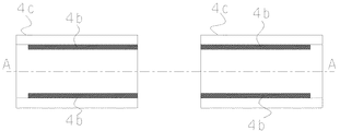
タブレット4aは、一つの側面に開口端を備えた立方体であり、内部にコイル2を収納するためのスペースを有している。タブレット4aの上面と底面とは同じ形状をしており、製造工程を通して実装面へと加工される。図4に示す様に、実装面の外形は長方形であり、この長方形を構成する4辺のうち、開口端に一番近い辺を短辺とし、短辺と隣接する辺を長辺とする。実装面は、短辺方向の両端部にそれぞれ、実装面と垂直に突出した突部4cを備え、突部4cと隣接する位置にそれぞれ、細長いスリット4bを備えている。スリット4bからは、コイル2の引き出し端部2cが引き出される。
The element body used in Example 1 will be described. The
The
図5〜図9を用いて、表面実装インダクタの製造方法を説明する。図5〜図8は、製造方法を説明するためのA−A断面図であり、図9は、素体の実装面の平面図である。 A method for manufacturing a surface-mount inductor will be described with reference to FIGS. 5 to 8 are AA cross-sectional views for explaining the manufacturing method, and FIG. 9 is a plan view of the mounting surface of the element body.
図5(a)に示すように、コイル2の、巻軸の両側からそれぞれ、磁性体コア3を挿入する。図5(b)に示すように、磁性体コア3とコイル2の間には、隙間が設けられている。
As shown in FIG. 5A, the
次に、絶縁体を成形するための金型を用意する。図6(a)に示すように、金型6aは、1つの面に開口端を備えた立方体であり、内部にコイル2と磁性体コア3を収納するためのスペースを有している。この金型6aに、磁性体コア3が2つ挿入されたコイル2を入れる。コイル2の引き出し端部は、コイル2から金型6aの開口端に向かう方向へ引き出される。図6(b)に示すように、絶縁性の樹脂を注入する。絶縁性の樹脂は、磁性体コア3とコイル2を密閉する。また、絶縁性の樹脂は、磁性体コア3とコイル2の間に設けられた隙間に入る。この状態で、絶縁性の樹脂を脱気することによって、コイル2と磁性体コア3とを内蔵した絶縁体5を得ることができる。絶縁体5は、磁性体コア3に対してコイル2を密閉するので、コイル2と磁性体コア3は接触しない。
Next, a mold for forming the insulator is prepared. As shown in FIG. 6A, the mold 6a is a cube having an open end on one surface, and has a space for accommodating the
絶縁体5を金型6aから取り出し、図7(a)に示すように、絶縁体5の両側に、タブレット4aを、開口端が向き合うようにして配置する。図7(b)に示すように、2つのタブレット4aが、コイル2および磁性体コア3を密閉した絶縁体5を内蔵するように、それぞれのタブレット4aを移動する。その後、コイル2の引き出し端部2cを、タブレット4aの片方のスリット4bから引き出す。引き出し端部2cを、タブレット4aの実装面に延在させ、もう片方のスリット4bに入れる。
The
次に、素体を成形するための金型を用意する。図8(a)に示すように、金型6bは、1つの面に開口端を備えた立方体であり、内部にコイル2と磁性体コア3とタブレット4aと絶縁体5とを収納するためのスペースを有している。この金型6bに、コイル2と磁性体コア3とを絶縁体5とを内蔵したタブレット4aを入れる。コイル2の引き出し端部は、コイル2から金型6bの開口端に向かう方向へ引き出される。その後、蓋6cを、金型6bの開口面から被せる。次に、図8(b)に示すように、2つのタブレット4aを加熱・圧縮することにより、コイル2と磁性体コア3と絶縁体5を内蔵した素体4を得ることができる。引き出し端部2cは、実装面の表面に露出する様に埋め込まれた状態で固定されている。
Next, a mold for forming the element body is prepared. As shown in FIG. 8 (a), the
次に、引き出し端部2cを外部端子に加工する方法について説明する。
素体4の実装面に露出・延在している引き出し端部2cにレーザーを照射し、絶縁被覆を剥離する。平角線を用いているので、レーザー剥離の条件設定が容易である。次に、引き出し端部2cにNiとCrとを所定の割合で同時にスパッタリングしてNi−Cu層を形成し、続いてSnをスパッタリングしてSn層を形成することにより、図9に示すように、外部端子7を形成することができる。
平角線を用いているので、丸線に比べて固着強度が強く、端子平坦度も高い。このまま外部端子として使用しても良いし、必要に応じて、さらに金属体を取り付け、外部端子としても良い。
Next, a method for processing the
The
Since a rectangular wire is used, the fixing strength is higher than that of the round wire, and the terminal flatness is also high. It may be used as an external terminal as it is, or a metal body may be further attached as necessary to serve as an external terminal.
以上より、表面実装インダクタを製造することができる。図10に示すように、表面実装インダクタ1は、コイルの第1の巻回部2aと第2の巻回部2bとを絶縁体5で密閉して覆っているので、タブレット4aで封止する際、コイル2を構成する導線間に磁性粉が入り込まず、電気的な耐圧が低下しない。
From the above, a surface mount inductor can be manufactured. As shown in FIG. 10, the surface-mount inductor 1 is sealed with the
実施例1の表面実装インダクタは、磁性体コアに対してコイルの巻回部を絶縁体で密閉して覆っているので、タブレットと同じ材質の磁性体コアあるいは導電性の磁性体コアを使用した場合であっても、電気的な耐圧が低下しない。
また、内蔵されたコイルの形状が左右対称で、それぞれの引き出し端部の引き出し位置から外部端子への距離が同じなので、極性を持たない。極性を持たない表面実装インダクタは、使用時にいずれの外部端子から入力しても、電気的特性が同じなので、極性を示すマーキングを印字する必要が無い。マーキングを印字する必要がないので、製造コストを抑えることができる。
In the surface mount inductor of Example 1, since the coil winding portion was hermetically covered with an insulator with respect to the magnetic core, a magnetic core made of the same material as the tablet or a conductive magnetic core was used. Even in this case, the electrical breakdown voltage does not decrease.
Moreover, since the shape of the built-in coil is bilaterally symmetric and the distance from the drawing position of each drawing end to the external terminal is the same, it has no polarity. A surface mount inductor having no polarity has the same electrical characteristics regardless of whether it is input from any external terminal at the time of use, and therefore there is no need to print markings indicating polarity. Since there is no need to print markings, manufacturing costs can be reduced.
以下、本発明の表面実装インダクタ及びその製造方法の実施例2を、図11〜図14を参照して説明する。実施例1と同じものを使用する場合は、実施例1と同じ番号を付する。 Hereinafter, a second embodiment of the surface mount inductor and the manufacturing method thereof according to the present invention will be described with reference to FIGS. When using the same thing as Example 1, the same number as Example 1 is attached.
図11に示すように、絶縁体を成形するための金型6aを用意する。磁性体コア3を内蔵したコイル2を、金型6aに入れる。コイル2の引き出し端部は、コイル2から金型6aの開口端に向かう方向へ引き出される。図11(b)に示すように、絶縁体5を注入し、コイル2と磁性体コア3とを密閉する。このとき、絶縁性の樹脂は磁性体コア3とコイル2の間に入らない。この後、絶縁性の樹脂を脱気することにより、コイル2と磁性体コア3とを内蔵した絶縁体5を形成することができる。絶縁体5は、磁性体コア3に対してコイル2を密閉しないので、コイル2の内側と磁性体コア3は接触している。
As shown in FIG. 11, a mold 6a for forming an insulator is prepared. The
絶縁体5を金型6aから取り出し、図12(a)に示すように、絶縁体5の両側に、タブレット4aを、開口端が向き合うようにして配置する。図12(b)に示すように、2つのタブレット4aが、コイル2および磁性体コア3を密閉した絶縁体5を内蔵するように、それぞれのタブレット4aを移動する。その後、コイル2の引き出し端部2cを、タブレット4aの片方のスリット4bから引き出す。引き出し端部2cを、タブレット4aの実装面に延在させ、もう片方のスリット4bに入れる。
The
図13(a)に示すように、素体を成形するための金型6bを用意し、コイル2と磁性体コア3とを内蔵した2つのタブレット4aを入れる。コイル2の引き出し端部は、コイル2から金型6bの開口端に向かう方向へ引き出される。その後、蓋6cを、金型6bの開口面から被せる。次に、図13(b)に示すように、2つのタブレット4aを加熱・圧縮することにより、コイル2と磁性体コア3と絶縁体5を内蔵した素体4を得ることができる。引き出し端部2cが、その表面が実装面の表面に露出する様に埋め込まれた状態で固定される。
As shown in FIG. 13A, a
この後、実施例1と同様に、引き出し端部2cを外部端子7へと加工することによって、表面実装インダクタを製造することができる。図14に示すように、表面実装インダクタ11は、コイルの第1の巻回部2aと第2の巻回部2bとを絶縁体5で密閉しているので、コイルを構成する導線間に磁性粉が入り込まず、電気的な耐圧が低下しない。
Thereafter, similarly to the first embodiment, the surface-mount inductor can be manufactured by processing the lead-out
実施例2の表面実装インダクタは、空芯コイルにコアを挿入しているが、磁性体コアに直接、導線を巻回してコイルを形成しても良い。コイルと磁性体コアの距離が近いので、高いインダクタンス値を有する表面実装インダクタを製造することができる。 In the surface mount inductor according to the second embodiment, the core is inserted into the air-core coil, but the coil may be formed by winding a conductive wire directly around the magnetic core. Since the distance between the coil and the magnetic core is short, a surface mount inductor having a high inductance value can be manufactured.
以上、本発明の表面実装インダクタ及びその製造方法の実施例を述べたが、本発明はこの実施例に限られるものではない。磁性体コアの材質は、フェライトでもよいし、磁性粉を含むものでも良い。タブレットの一部分を磁性体コアに置き換えても良いし、磁性体コアの一部分をタブレットに置き換えても良い。また、磁性体コアを使用しなくても良い。コイルを形成する導線は、平角線を用いたが、丸線でも良いし、他の断面形状の線材を用いても良い。コイルの引き出し端部を外部電極として使用しているが、外部電極の代わりに、コイルの両端に電気的に接続された導体を使用しても良い。 As mentioned above, although the Example of the surface mount inductor of this invention and its manufacturing method was described, this invention is not limited to this Example. The material of the magnetic core may be ferrite or may contain magnetic powder. A part of the tablet may be replaced with a magnetic core, or a part of the magnetic core may be replaced with a tablet. Moreover, it is not necessary to use a magnetic core. The conductor wire forming the coil is a rectangular wire, but it may be a round wire or a wire having another cross-sectional shape. The lead end of the coil is used as an external electrode, but a conductor electrically connected to both ends of the coil may be used instead of the external electrode.
1、11 表面実装インダクタ
2 コイル
2a 第1の巻回部
2b 第2の巻回部
2c 引き出し端部
3 磁性体コア
4 素体
4a タブレット
4b スリット
4c 突部
5 絶縁体
6a、6b 金型
6c 蓋
7 外部電極
DESCRIPTION OF
Claims (10)
実装面上に延在し、コイルの両端とそれぞれ電気的に接続される外部端子を有し、
該素体は、磁性粉と樹脂を含む封止材の圧縮成形体であり、
該絶縁体は、該磁性体コアおよび該巻回部を密閉することを特徴とする表面実装インダクタ。 A coil composed of a winding part and a lead-out end part, a magnetic core, an insulator containing the winding part of the coil and the magnetic core, and an element body containing the insulator and containing magnetic powder; In surface mount inductors with
It has external terminals that extend on the mounting surface and are electrically connected to both ends of the coil.
The element body is a compression molded body of a sealing material containing magnetic powder and resin,
The surface mount inductor, wherein the insulator seals the magnetic core and the winding portion.
該コイルを形成する工程と、
該コイルの巻回部を該絶縁体で密閉する工程と、
該絶縁体を該素体に内蔵するように、磁性粉と樹脂を含み、該絶縁体を包囲する封止材に圧力をかけて圧縮成形して該素体を形成する工程と、
を備えていることを特徴とする表面実装インダクタの製造方法。 A method for manufacturing a surface-mount inductor comprising: a coil composed of a winding part and a lead-out end part; an insulator including the winding part of the coil; and an element including the insulator and including magnetic powder. In
Forming the coil;
Sealing the coil winding with the insulator;
A step of forming the element body by compressing and molding a sealing material that includes magnetic powder and a resin so as to incorporate the insulator in the element body and that surrounds the insulator; and
A method for manufacturing a surface mount inductor, comprising:
該コイルを形成する工程と、
該コイルの巻回部および該磁性体コアを、該絶縁体で密閉する工程と、
該絶縁体を該素体に内蔵するように、磁性粉と樹脂を含み、該絶縁体を包囲する封止材に圧力をかけて圧縮成形して該素体を形成する工程と、
を備えていることを特徴とする表面実装インダクタの製造方法。 A surface provided with a coil composed of a winding part and a lead-out end part, a magnetic core, an insulator containing the winding part of the coil, and an element body containing the insulator and containing magnetic powder In the manufacturing method of the mounted inductor,
Forming the coil;
Sealing the winding portion of the coil and the magnetic core with the insulator;
A step of forming the element body by compressing and molding a sealing material that includes magnetic powder and a resin so as to incorporate the insulator in the element body and that surrounds the insulator; and
A method for manufacturing a surface mount inductor, comprising:
前記磁性体コアと前記コイルが接触しないように、前記絶縁体が前記コイルを覆うことを特徴とする、請求項7に記載の表面実装インダクタの製造方法。 In the step of sealing the coil and the magnetic core with the insulator,
The method of manufacturing a surface mount inductor according to claim 7, wherein the insulator covers the coil so that the magnetic core and the coil do not contact each other.
Priority Applications (1)
| Application Number | Priority Date | Filing Date | Title |
|---|---|---|---|
| JP2015123403A JP6332159B2 (en) | 2015-06-19 | 2015-06-19 | Surface mount inductor and manufacturing method thereof |
Applications Claiming Priority (1)
| Application Number | Priority Date | Filing Date | Title |
|---|---|---|---|
| JP2015123403A JP6332159B2 (en) | 2015-06-19 | 2015-06-19 | Surface mount inductor and manufacturing method thereof |
Publications (2)
| Publication Number | Publication Date |
|---|---|
| JP2017011047A JP2017011047A (en) | 2017-01-12 |
| JP6332159B2 true JP6332159B2 (en) | 2018-05-30 |
Family
ID=57764241
Family Applications (1)
| Application Number | Title | Priority Date | Filing Date |
|---|---|---|---|
| JP2015123403A Active JP6332159B2 (en) | 2015-06-19 | 2015-06-19 | Surface mount inductor and manufacturing method thereof |
Country Status (1)
| Country | Link |
|---|---|
| JP (1) | JP6332159B2 (en) |
Families Citing this family (3)
| Publication number | Priority date | Publication date | Assignee | Title |
|---|---|---|---|---|
| CN107170551B (en) * | 2017-05-18 | 2023-07-07 | 平顶山市津电智能科技有限公司 | Waterproof transformer |
| CN107785150A (en) * | 2017-10-31 | 2018-03-09 | 深圳振华富电子有限公司 | The SMD inductor of High-reliability large-power |
| JP7117843B2 (en) | 2017-12-26 | 2022-08-15 | 日立建機株式会社 | working machine |
Family Cites Families (7)
| Publication number | Priority date | Publication date | Assignee | Title |
|---|---|---|---|---|
| JPS62235706A (en) * | 1986-04-05 | 1987-10-15 | Tdk Corp | Inductance device |
| JPH05283251A (en) * | 1992-03-31 | 1993-10-29 | Kawatetsu Magunetsukusu Kk | Pot type inductor |
| JP2003017329A (en) * | 2001-06-28 | 2003-01-17 | Tabuchi Electric Co Ltd | Inductance element |
| JP5935309B2 (en) * | 2011-12-15 | 2016-06-15 | スミダコーポレーション株式会社 | Coil parts |
| JP6405609B2 (en) * | 2012-10-03 | 2018-10-17 | Tdk株式会社 | Inductor element and manufacturing method thereof |
| JP3186098U (en) * | 2013-07-05 | 2013-09-19 | スミダコーポレーション株式会社 | Core members and coil parts |
| JP2016063158A (en) * | 2014-09-19 | 2016-04-25 | Ntn株式会社 | Inductor |
-
2015
- 2015-06-19 JP JP2015123403A patent/JP6332159B2/en active Active
Also Published As
| Publication number | Publication date |
|---|---|
| JP2017011047A (en) | 2017-01-12 |
Similar Documents
| Publication | Publication Date | Title |
|---|---|---|
| KR101866150B1 (en) | Surface-mounted inductor and manufacturing method therefor | |
| JP6179491B2 (en) | Surface mount inductor and manufacturing method thereof | |
| KR20180073488A (en) | Surface-mount inductor | |
| JP6299567B2 (en) | Surface mount inductor and manufacturing method thereof | |
| US11657955B2 (en) | Surface mount inductor | |
| JP6197829B2 (en) | Surface mount inductor | |
| JP2017069460A (en) | Coil component and manufacturing method therefor | |
| JP2017201718A (en) | Surface mounting inductor and manufacturing method thereof | |
| JP6332159B2 (en) | Surface mount inductor and manufacturing method thereof | |
| JP6414612B2 (en) | Surface mount inductor and manufacturing method thereof | |
| JP6379468B2 (en) | Wire wound electronic components | |
| JP6503975B2 (en) | Method of manufacturing surface mount inductor | |
| KR20140071756A (en) | Inductor and inductor manufacturing method | |
| CN105845318A (en) | Surface-mount inductor and method for manufacturing the same | |
| JP6172214B2 (en) | Manufacturing method of surface mount inductor | |
| JP6332160B2 (en) | Surface mount inductor and manufacturing method thereof | |
| WO2017115603A1 (en) | Surface mount inductor and method for manufacturing same | |
| JP6287761B2 (en) | Surface mount inductor and manufacturing method thereof | |
| JP2016092096A (en) | Manufacturing method of surface mount inductor | |
| JP6365242B2 (en) | Manufacturing method of surface mount inductor | |
| JP6623928B2 (en) | Common mode filter | |
| JP6206164B2 (en) | Surface mount inductor | |
| JP6623929B2 (en) | Common mode filter | |
| JP6299560B2 (en) | Surface mount inductor and manufacturing method thereof | |
| JP6623930B2 (en) | Common mode filter |
Legal Events
| Date | Code | Title | Description |
|---|---|---|---|
| A711 | Notification of change in applicant |
Free format text: JAPANESE INTERMEDIATE CODE: A711 Effective date: 20170111 |
|
| RD03 | Notification of appointment of power of attorney |
Free format text: JAPANESE INTERMEDIATE CODE: A7423 Effective date: 20170116 |
|
| A521 | Written amendment |
Free format text: JAPANESE INTERMEDIATE CODE: A523 Effective date: 20170203 |
|
| A131 | Notification of reasons for refusal |
Free format text: JAPANESE INTERMEDIATE CODE: A131 Effective date: 20170328 |
|
| A521 | Written amendment |
Free format text: JAPANESE INTERMEDIATE CODE: A523 Effective date: 20170426 |
|
| A131 | Notification of reasons for refusal |
Free format text: JAPANESE INTERMEDIATE CODE: A131 Effective date: 20170725 |
|
| A521 | Written amendment |
Free format text: JAPANESE INTERMEDIATE CODE: A523 Effective date: 20170804 |
|
| A131 | Notification of reasons for refusal |
Free format text: JAPANESE INTERMEDIATE CODE: A131 Effective date: 20171212 |
|
| A521 | Written amendment |
Free format text: JAPANESE INTERMEDIATE CODE: A523 Effective date: 20180109 |
|
| TRDD | Decision of grant or rejection written | ||
| A01 | Written decision to grant a patent or to grant a registration (utility model) |
Free format text: JAPANESE INTERMEDIATE CODE: A01 Effective date: 20180403 |
|
| A61 | First payment of annual fees (during grant procedure) |
Free format text: JAPANESE INTERMEDIATE CODE: A61 Effective date: 20180416 |
|
| R150 | Certificate of patent or registration of utility model |
Ref document number: 6332159 Country of ref document: JP Free format text: JAPANESE INTERMEDIATE CODE: R150 |