JP6325846B2 - Method for creating a floor plan of a semiconductor integrated circuit - Google Patents
Method for creating a floor plan of a semiconductor integrated circuit Download PDFInfo
- Publication number
- JP6325846B2 JP6325846B2 JP2014046196A JP2014046196A JP6325846B2 JP 6325846 B2 JP6325846 B2 JP 6325846B2 JP 2014046196 A JP2014046196 A JP 2014046196A JP 2014046196 A JP2014046196 A JP 2014046196A JP 6325846 B2 JP6325846 B2 JP 6325846B2
- Authority
- JP
- Japan
- Prior art keywords
- floor plan
- timing
- information
- path
- placement
- Prior art date
- Legal status (The legal status is an assumption and is not a legal conclusion. Google has not performed a legal analysis and makes no representation as to the accuracy of the status listed.)
- Expired - Fee Related
Links
- 239000004065 semiconductor Substances 0.000 title claims description 32
- 238000000034 method Methods 0.000 title claims description 31
- 238000005457 optimization Methods 0.000 claims description 14
- 239000000284 extract Substances 0.000 claims description 5
- 230000002093 peripheral effect Effects 0.000 claims description 4
- 230000008569 process Effects 0.000 description 14
- 102100040862 Dual specificity protein kinase CLK1 Human genes 0.000 description 12
- 238000010586 diagram Methods 0.000 description 9
- 101000749294 Homo sapiens Dual specificity protein kinase CLK1 Proteins 0.000 description 3
- 238000013461 design Methods 0.000 description 3
- 238000000605 extraction Methods 0.000 description 3
- 238000012545 processing Methods 0.000 description 3
- 230000003068 static effect Effects 0.000 description 3
- 102100040844 Dual specificity protein kinase CLK2 Human genes 0.000 description 2
- 101000749291 Homo sapiens Dual specificity protein kinase CLK2 Proteins 0.000 description 2
- 230000008859 change Effects 0.000 description 2
- 230000012447 hatching Effects 0.000 description 2
- 238000007796 conventional method Methods 0.000 description 1
- 230000006870 function Effects 0.000 description 1
- 238000012986 modification Methods 0.000 description 1
- 230000004048 modification Effects 0.000 description 1
- 238000004088 simulation Methods 0.000 description 1
- 230000001360 synchronised effect Effects 0.000 description 1
- 238000001308 synthesis method Methods 0.000 description 1
Images


Landscapes
- Design And Manufacture Of Integrated Circuits (AREA)
Description
本発明は、半導体集積回路のネットリストに対応するレイアウトのフロアプランを作成する半導体集積回路のフロアプラン作成方法に関するものである。 The present invention relates to a method for creating a floor plan for a semiconductor integrated circuit, which creates a floor plan for a layout corresponding to a net list of the semiconductor integrated circuit.
図8は、従来の半導体集積回路のレイアウトのフロアプランを作成する各工程を表す一例のフローチャートである。
同図に示すように、従来、半導体集積回路のレイアウトのフロアプランを作成する場合、まず、フロアプランの作成領域を、フロアプランの見積りの配置面積の領域とする制約をかけて、半導体集積回路のネットリストに含まれるマクロセルの配置を行う(ステップS21)。
FIG. 8 is a flowchart of an example showing each process of creating a floor plan of a conventional semiconductor integrated circuit layout.
As shown in the figure, conventionally, when creating a floor plan for a layout of a semiconductor integrated circuit, first, the area for creating the floor plan is constrained to be an area of the estimated layout area of the semiconductor integrated circuit. The macro cells included in the netlist are arranged (step S21).
続いて、フロアプランの作成領域内に、ネットリストに含まれるスタンダードセルの配置を行い(ステップS22)、さらに、タイミングエラーの発生を削減するためのタイミング最適化を行う(ステップS23)。 Subsequently, standard cells included in the netlist are arranged in the floor plan creation area (step S22), and further, timing optimization is performed to reduce the occurrence of timing errors (step S23).
続いて、クロックツリーの生成を行い(ステップS24)、マクロセルおよびスタンダードセル間の各々のパスの配線を行ってフロアプランを作成する(ステップS25)。 Subsequently, a clock tree is generated (step S24), and wiring of each path between the macro cell and the standard cell is performed to create a floor plan (step S25).
続いて、フロアプランから、各々のパスの遅延情報等を含む遅延情報データを作成する(ステップS26)。 Subsequently, delay information data including delay information and the like of each path is created from the floor plan (step S26).
続いて、遅延情報データに基づいて、ネットリストのタイミング解析を行って、タイミングを考慮する必要のないパスであるフォルスパスの情報を抽出する(ステップS27)。 Subsequently, based on the delay information data, timing analysis of the netlist is performed, and information on a false path that is a path that does not need to take timing into consideration is extracted (step S27).
続いて、タイミング解析の結果、フロアプランを変更する必要があるかないかを判定する(ステップS28)。
ステップS28でフロアプランを変更する必要があると判定された場合(ステップS28でYES)、ステップS21へ戻り上記処理を再び行う。一方、フロアプランを変更する必要がないと判定された場合(ステップS28でNO)、プロアプランの作成を終了する。
Subsequently, as a result of the timing analysis, it is determined whether or not the floor plan needs to be changed (step S28).
If it is determined in step S28 that the floor plan needs to be changed (YES in step S28), the process returns to step S21 and the above process is performed again. On the other hand, when it is determined that there is no need to change the floor plan (NO in step S28), the creation of the pro-plan is terminated.
半導体集積回路の大規模化に伴い、数百数千のマクロセル(メモリを含む)およびスタンダードセル間の接続を考慮しながら、上記のように、マクロセルおよびスタンダードセルの配置、タイミング最適化、クロックツリーの生成(CTS)、各々のパスの配線等を経てフロアプランを作成し、フロアプランから遅延情報データを作成し、遅延情報データに基づいてフォルトパスを抽出するまでには数日の時間を必要とする。 As the scale of semiconductor integrated circuits increases, considering the connection between hundreds and thousands of macro cells (including memory) and standard cells, as described above, the arrangement of macro cells and standard cells, timing optimization, and clock tree It takes several days to create a floor plan through the generation of data (CTS), wiring of each path, etc., create delay information data from the floor plan, and extract the fault path based on the delay information data And
フォルスパスの情報を追加したタイミング制約をかけて、スタンダードセルの配置、タイミング最適化および各々のパスの配線を行うことができれば、フォルスパスのタイミング最適化が行われるのを防ぐことができ、そのための処理時間を節約することができる。また、フォルスパスのタイミング最適化を省くことにより、回路規模の増加を防ぐことができるため、その分のレイアウト面積および消費電力も削減することができる。従って、なるべく多くのフォルスパスを早期に抽出できることが望ましい。 If timing constraints with added false path information can be applied and standard cell placement, timing optimization, and routing of each path can be performed, false path timing optimization can be prevented. Processing time can be saved. Further, by omitting false path timing optimization, it is possible to prevent an increase in circuit scale, thereby reducing the layout area and power consumption accordingly. Therefore, it is desirable to extract as many false paths as possible at an early stage.
しかし、従来のフロアプランの作成方法では、タイミング最適化を行ってフロアプランを作成した後、フロアプランから作成した遅延情報データに基づいてフォルスパスを抽出する。そのため、フォルスパスを抽出するまでに数日の時間を必要とし、TAT(ターンアラウンドタイム)に大きな影響を与えている。また、タイミング解析の結果、フロアプランのやり直しが必要になった場合、数日の時間をかけて作成された遅延情報データおよびフォルスパスの情報が無駄になる。 However, in the conventional method for creating a floor plan, after performing timing optimization and creating a floor plan, a false path is extracted based on delay information data created from the floor plan. Therefore, it takes several days to extract the false path, which has a great influence on TAT (turnaround time). In addition, when the floor plan needs to be redone as a result of the timing analysis, the delay information data and false path information created over several days are wasted.
本発明に関連性のある先行技術文献として、特許文献1〜3がある。
As prior art documents relevant to the present invention, there are
特許文献1には、フォルスパス自動生成ツールが生成した複数のフォルスパスの経路に対して、それぞれ所定のタイミング仕様に基づいたタイミング解析を施し、所定のタイミング仕様を満たさない結果に対応したフォルスパスを抽出して、フォルスパス設定を利用した各種の処理に要する時間の短縮化を効果的に促進させるようにしたフォルスパス自動抽出装置及びフォルスパス自動抽出方法が記載されている。
特許文献2には、RTL論理回路において、FFから外部出力端子とのパスや同一クロックソースを持つFF間のパスのうち、データ遅延時間の調整が必要のないフォルスパス設定を容易にするために、フォルスパスであることを明示するダミーモジュールを挿入し、ダミーモジュールが挿入されたRTL論理回路を読み込んでゲートレベル回路を生成する半導体設計支援装置および半導体設計支援方法が記載されている。
In
特許文献3には、半導体装置のレイアウト設計において、回路のクロック情報に基づいて、回路におけるクロックツリーが互いに排他となり、重複部分がないようにクロックツリーを分割するために必要となるフォルスパス及びクロックツリー上に存在するフリップフロップ以外のポイントをリーフ扱いするためのリーフポイントを抽出するクロック合成方法が記載されている。
In
本発明の目的は、前記従来技術の問題点を解消し、フロアプランの作成工程の早期に多くのフォルスパスを抽出して、フォルスパスを考慮したフロアプランのタイミング最適化を行うことができる半導体集積回路のフロアプラン作成方法を提供することにある。 An object of the present invention is to solve the above-mentioned problems of the prior art, extract a lot of false paths early in the floor plan creation process, and perform a floor plan timing optimization considering the false paths. An object of the present invention is to provide a method for creating a floor plan of an integrated circuit.
上記目的を達成するために、本発明は、コンピュータが、半導体集積回路のネットリストに対応するレイアウトのフロアプランを作成する半導体集積回路のフロアプラン作成方法であって、
前記コンピュータが、
前記フロアプランの作成領域を、前記フロアプランの見積りよりも大きい配置面積の領域とする制約をかけて、かつ、タイミングを考慮することなく、前記ネットリストに含まれるマクロセルの仮配置を行う第1ステップと、
前記タイミングを考慮することなく、前記フロアプランの作成領域内に、前記ネットリストに含まれるスタンダードセルの仮配置を行う第2ステップと、
前記タイミングを考慮することなく、クロックツリーの仮生成を行う第3ステップと、
前記タイミングを考慮することなく、前記仮配置が行われたマクロセルおよびスタンダードセル間の各々のパスの仮配線を行って仮フロアプランを作成する第4ステップと、
前記仮フロアプランから、前記仮生成が行われたクロックツリーの各々のクロックの遅延情報、および、前記仮配線が行われた各々のパスの遅延情報を含む第1遅延情報データを作成する第5ステップと、
前記第1遅延情報データに基づいて、前記ネットリストのタイミング解析を行ってフォルスパスの情報、および、前記マクロセル間の配置の制約の情報を抽出する第6ステップと、
前記フロアプランの作成領域を、前記フロアプランの見積りの配置面積の領域とする制約をかけて、かつ、前記マクロセル間の配置の制約の情報を追加したタイミング制約をかけて、前記マクロセルの本配置を行う第7ステップと、
前記フォルスパスの情報を追加したタイミング制約をかけて、前記フロアプランの作成領域内に、前記スタンダードセルの本配置を行う第8ステップと、
前記フォルスパスの情報を追加したタイミング制約をかけて、タイミング最適化を行う第9ステップと、
前記クロックツリーの各々のクロックの遅延情報を追加したタイミング制約をかけて、前記クロックツリーの本生成を行う第10ステップと、
前記フォルスパスの情報を追加したタイミング制約をかけて、前記本配置が行われたマクロセルおよびスタンダードセル間の各々のパスの本配線を行って本フロアプランを作成する第11ステップとを実行することを特徴とする半導体集積回路のフロアプラン作成方法を提供するものである。
In order to achieve the above object, the present invention provides a floor plan creation method for a semiconductor integrated circuit, in which a computer creates a floor plan of a layout corresponding to a net list of the semiconductor integrated circuit,
The computer is
A first placement of macrocells included in the netlist is constrained so that the floorplan creation region is a region having a larger layout area than the estimated floorplan and without considering timing. Steps,
A second step of tentatively arranging standard cells included in the netlist in the floor plan creation area without considering the timing;
A third step of temporarily generating a clock tree without considering the timing;
A fourth step of creating a temporary floor plan by performing temporary wiring of each path between the macro cell and the standard cell in which the temporary placement is performed without considering the timing;
First delay information data including delay information of each clock of the clock tree in which the temporary generation has been performed and delay information of each path in which the temporary wiring has been performed is generated from the temporary floor plan. Steps,
Based on the first delay information data, a sixth step of performing timing analysis of the netlist to extract information on false paths and information on arrangement restrictions between the macro cells;
The placement of the floor plan is constrained to be an area of the floor plan estimated placement area, and the placement of the macro cell is placed with timing constraints to which information on placement constraints between the macro cells is added. A seventh step of performing
Applying the timing constraint to which the false path information has been added, the eighth step of performing the regular placement of the standard cells in the floor plan creation area;
A ninth step of optimizing the timing by applying a timing constraint to which the false path information is added;
A tenth step of performing the main generation of the clock tree by applying a timing constraint to which delay information of each clock of the clock tree is added;
Executing the eleventh step of creating the floor plan by performing the main wiring of each path between the macro cell and the standard cell in which the main placement has been performed, with timing constraints added with the false path information. The present invention provides a method for creating a floor plan of a semiconductor integrated circuit.
前記コンピュータが、さらに、前記本フロアプランから、前記本生成が行われたクロックツリーの各々のクロックの遅延情報、および、前記本配線が行われた各々のパスの遅延情報を含む第2遅延情報データを作成する第12ステップと、
前記第2遅延情報データに基づいて、前記ネットリストのタイミング解析を行う第13ステップとを実行することが好ましい。
The computer further includes second delay information including delay information of each clock of the clock tree in which the main generation has been performed, and delay information of each path in which the main wiring has been performed, from the floor plan. A twelfth step of creating data;
It is preferable to execute a thirteenth step of analyzing the timing of the netlist based on the second delay information data.
また、前記第1ステップにより、前記フロアプランの作成領域内の外周部に沿って前記マクロセルの仮配置を行い、前記第2ステップにより、前記フロアプランの作成領域内の中央部に前記スタンダードセルの配置を行うことが好ましい。 Further, the macro cell is provisionally arranged along an outer peripheral portion in the floor plan creation area in the first step, and the standard cell is placed in a central part in the floor plan creation area in the second step. It is preferable to perform the arrangement.
また、前記第1ステップにより、前記フロアプランの作成領域を、前記フロアプランの見積りの2倍以上、5倍以下の配置面積の領域とする制約をかけて、前記マクロセルの仮配置を行うことが好ましい。 In addition, the macro cell provisional placement may be performed with the constraint that the floor plan creation region is a region having an arrangement area that is two to five times the estimate of the floor plan, according to the first step. preferable.
また、前記第6ステップにより、前記マクロセル間の配置の制約の情報を、前記フォルスパスの情報よりも先に抽出し、
前記第7ステップにより、前記マクロセルの本配置を行い、
前記第6ステップにより、前記フォルスパスの情報を抽出する間に、前記第8ステップにより、前記スタンダードセルの本配置を行うことが好ましい。
Further, the sixth step extracts the information on the restriction of the arrangement between the macro cells before the information of the false path,
According to the seventh step, the macro cell is placed in a main position,
Preferably, the standard cells are permanently arranged in the eighth step while the false path information is extracted in the sixth step.
また、前記第6ステップにより、さらに、クリティカルパスの情報を抽出し、
前記クリティカルパスの情報を追加したタイミング制約をかけて、前記スタンダードセルの本配置、前記タイミング最適化、および、前記各々のパスの本配線を行うことが好ましい。
Further, the sixth step further extracts critical path information,
It is preferable to perform the main placement of the standard cells, the timing optimization, and the main wiring of each of the paths, with timing constraints added with the critical path information.
本発明によれば、タイミング最適化のためのタイミング制約をかけることなく、仮配置、クロックツリーの仮生成、仮配線を行って、短時間で仮フロアプランを作成し、作成した仮フロアプランから第1遅延情報データを作成して本フロアプランの作成にフィードバックすることにより、フロアプランの作成工程の早期に多くのフォルスパスを抽出し、抽出したフォルスパスを考慮して本フロアプランのタイミング最適化を行うことができる。
また、本フロアプランに早期にフィードバックをかけて、タイミングエラーの発生を削減することができるため、作成した本フロアプランが無駄になることを削減し、TATを短縮することができる。
According to the present invention, temporary placement, clock tree temporary generation, and temporary wiring are performed without imposing timing constraints for timing optimization, and a temporary floor plan is created in a short time. By creating the first delay information data and feeding it back to the creation of this floor plan, many false paths are extracted early in the floor plan creation process, and the timing of this floor plan is optimized in consideration of the extracted false paths Can be made.
In addition, since this floor plan can be fed back early to reduce the occurrence of timing errors, the created floor plan can be reduced from being wasted and TAT can be shortened.
以下に、添付の図面に示す好適実施形態に基づいて、本発明の半導体集積回路のフロアプラン作成方法を詳細に説明する。 Hereinafter, a method for creating a floor plan of a semiconductor integrated circuit according to the present invention will be described in detail based on a preferred embodiment shown in the accompanying drawings.
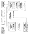
図1は、本発明の半導体集積回路のレイアウトのフロアプランを作成する各工程を表す一実施形態のフローチャート、図2は、図1に示す各工程で使用されるデータの流れを表す一例の概念図である。 FIG. 1 is a flowchart of an embodiment showing each process for creating a floor plan of a layout of a semiconductor integrated circuit according to the present invention, and FIG. 2 is an example concept showing a flow of data used in each process shown in FIG. FIG.
これらの図に示すように、本実施形態において、半導体集積回路のレイアウトのフロアプランを作成する場合、まず、仮フロアプランの制約、つまり、仮フロアプランの作成領域を、フロアプランの見積りの2倍以上、5倍以下の配置面積の領域とする制約をかけて、かつ、タイミング制約をかけることなく、つまり、タイミングを考慮することなく、半導体集積回路のネットリストに含まれるマクロセルの仮配置を行う(ステップS1)。 As shown in these drawings, in the present embodiment, when creating a floor plan of a layout of a semiconductor integrated circuit, first, restrictions on a temporary floor plan, that is, a provisional area of a temporary floor plan, are set to 2 of floor plan estimation. The provisional placement of the macrocells included in the netlist of the semiconductor integrated circuit can be performed without restricting the timing of the arrangement, and without restricting the timing of the arrangement area to the area of 5 times or more and 5 times or less. Perform (Step S1).
例えば、図3に示すように、メモリを含むマクロセル12を、マクロセル12同士の間隔を一律(例えば、100μm)に設定して、仮フロアプランの作成領域11内の外周部に沿って配置する。この時、マクロセル12間の配置の制約の情報を追加したタイミング制約や、フォルスパスの情報を追加したタイミング制約等のように、タイミング最適化を行うための、処理時間のかかるタイミング制約はかけない。
図3の例では、同じ種類のハッチがかけられたブロック(マクロセル12およびスタンダードセル14)間のタイミング制約が厳しいことを表しているが、仮フロアプランでの仮配置においては半導体集積回路の動作タイミングを考慮する必要はない。
For example, as shown in FIG. 3, the
In the example of FIG. 3, the timing constraint between the blocks (the
なお、図3の仮フロアプランの例は、各マクロの大きさは同じであるが、マクロ間の間隔を一律に広く取った場合を示しており、マクロ間の配線は容易に行えることがわかる。 The example of the temporary floor plan in FIG. 3 shows the case where the macros have the same size, but the intervals between the macros are uniformly wide, and it can be seen that wiring between the macros can be easily performed. .
続いて、タイミングを考慮することなく、仮フロアプランの作成領域11内に、ネットリストに含まれるスタンダードセルの仮配置を行う(ステップS2)。
Subsequently, the standard cells included in the netlist are temporarily arranged in the temporary floor
例えば、図3に示すように、スタンダードセル14、及び、マクロセル12は、仮フロアプランの作成領域11内で、セル間のスペースが取れるところであれば、どこに配置してもよい。
For example, as shown in FIG. 3, the
続いて、タイミングを考慮することなく、クロックツリーの仮生成を行う(ステップS3)。 Subsequently, the clock tree is tentatively generated without considering the timing (step S3).
続いて、タイミングを考慮することなく、仮配置が行われたマクロセルおよびスタンダードセル間の各々のパスの仮配線を行って仮フロアプランを作成する(ステップS4)。 Subsequently, a temporary floor plan is created by performing temporary wiring of each path between the macro cell and the standard cell in which temporary placement has been performed without considering the timing (step S4).
フロアプランの作成領域を、フロアプランの見積りの配置面積の領域とする制約をかけ、マクロ間の接続を考慮した場合、マクロセルおよびスタンダードセルの配置および配線を行うために数日の時間を必要とする。
これに対し、仮フロアプランの作成領域11を、フロアプランの見積りの2倍以上、5倍以下の配置面積の領域とする制約をかけた場合、仮配置および仮配線の自由度が高くなり、短時間で仮配置および仮配線を完了して仮フロアプランを作成することができる。
If the floorplan creation area is constrained to be the area of the floorplan estimate layout area and considering the connection between macros, it takes several days to place and route the macrocells and standard cells. To do.
On the other hand, when the provisional floor
続いて、仮フロアプランから、仮生成が行われたクロックツリーの各々のクロックの遅延情報、および、仮配線が行われた各々のパスの遅延情報等を含む第1遅延情報データを作成する(ステップS5)。 Subsequently, from the temporary floor plan, first delay information data including delay information of each clock of the clock tree in which temporary generation has been performed, delay information of each path in which temporary wiring has been performed, and the like is created ( Step S5).
ここで、第1遅延情報データは、仮生成が行われたクロックツリーの各々のクロック、および、仮配線が行われた各々のパスについて、セル(マクロセルおよびスタンダードセル)による遅延情報(遅延時間)、および、仮配線による遅延情報(遅延時間)を含む。
各々のセルによる遅延情報は、図2に示すセルライブラリに記憶されている。
Here, the first delay information data is the delay information (delay time) by the cell (macro cell and standard cell) for each clock of the clock tree in which temporary generation has been performed and each path in which temporary wiring has been performed. And delay information (delay time) due to temporary wiring.
The delay information for each cell is stored in the cell library shown in FIG.
仮フロアプランの作成領域11を、フロアプランの見積りの2倍以上、5倍以下の配置面積の領域とする制約をかけてマクロセルおよびスタンダードセルの仮配置および仮配線を行った場合、フロアプランの見積りの配置面積の領域とする制約をかけてマクロセルおよびスタンダードセルの本配置および本配線を行った場合と比べて配線長が長くなり、仮配線が行われた各々のパスの遅延時間は大幅に増加する。
If temporary placement and provisional wiring of macro cells and standard cells are performed with the restriction that the
続いて、第1遅延情報データに基づいて、例えば、シミュレーションによるネットリストのタイミング解析を行って、フォルスパスの情報、および、マクロセル間の配置の制約の情報等を抽出する(ステップS6)。 Subsequently, based on the first delay information data, for example, timing analysis of a netlist by simulation is performed, and false path information, information on arrangement restrictions between macro cells, and the like are extracted (step S6).
なお、ステップS6において、さらに、クリティカルパスの情報を抽出してもよい。 In step S6, critical path information may be further extracted.
ここで、クリティカルパスおよびフォルスパスについて説明する。 Here, the critical path and the false path will be described.
半導体集積回路内のある回路において、あるセル(マクロセルないしスタンダードセル)から、他のセルまでの信号の伝播が要求仕様に対して最も余裕がなくなる経路をクリティカルパスという。
また、静的タイミング解析ツールは、論理機能を考慮せず、回路のトポロジと遅延情報からクリティカルパスを見つけるため、現実の動作では意味のない(活性化されない)パスも一緒に解析することがある。このようなタイミングを考慮する必要のないパスをフォルスパスと呼ぶ。
In a certain circuit in the semiconductor integrated circuit, a path in which signal propagation from a certain cell (macro cell or standard cell) to another cell has the least margin with respect to a required specification is called a critical path.
In addition, since the static timing analysis tool finds a critical path from the circuit topology and delay information without considering the logic function, it may analyze a path that is meaningless (not activated) in actual operation. . A path that does not need to consider such timing is called a false path.
図4は、半導体集積回路内のパスを表す一例の概念図である。同図に示すように、半導体集積回路内の全てのパスは、次の(1)〜(4)に分類することができる。
(1)フリップフロップ(FF)からFFへのパス
(2)入力ポートからFFへのパス
(3)FFから出力ポートへのパス
(4)入力ポートから出力ポートへのパス
FIG. 4 is a conceptual diagram of an example showing a path in the semiconductor integrated circuit. As shown in the figure, all paths in the semiconductor integrated circuit can be classified into the following (1) to (4).
(1) Path from flip-flop (FF) to FF (2) Path from input port to FF (3) Path from FF to output port (4) Path from input port to output port
続いて、フォルスパスを含む回路の具体例を挙げて説明する。 Subsequently, a specific example of a circuit including a false path will be described.
図5は、フォルスパスを含む回路の構成を表す一例の回路図である。同図に示す回路は、直列に接続された3段のFF16,18,20を備えている。1段目のFF16は、第1クロックCLK1に同期して動作し、2段目および3段目のFF18,20は、第1クロックCLK1とは非同期関係にある第2クロックCLK2に同期して動作する。つまり、1段目のFF16のデータ出力端子から2段目のFF18のデータ入力端子に至るパスは非同期パスである。
FIG. 5 is a circuit diagram illustrating an example of a circuit configuration including a false path. The circuit shown in the figure includes three stages of
非同期パスは、タイミング解析を行う必要のないフォルスパスである。静的タイミング解析ツールでは、複数のクロックが定義されると、それらはすべて同期関係にあると推定され、それらの間のデータやパスはすべてタイミング解析の対象となる。従って、第1クロックCLK1と第2クロックCLK2とが非同期関係である場合には、それを明示するタイミング制約をかけて排除することが望ましい。 Asynchronous paths are false paths that do not require timing analysis. In the static timing analysis tool, when a plurality of clocks are defined, they are all estimated to be in a synchronous relationship, and all data and paths between them are subjected to timing analysis. Therefore, when the first clock CLK1 and the second clock CLK2 are in an asynchronous relationship, it is desirable to eliminate them by applying a timing constraint that clearly indicates the relationship.
続いて、図6は、フォルスパスを含む回路の構成を表す別の例の回路図である。同図に示す回路は、FF22と、マルチプレクサ24と、直列に接続された2段のFF26,28とを備えている。FF22は、クロックCLKに同期して、クロックCLKを2分周した分周クロックDIVCLKを出力する。マルチプレクサ24は、クロックCLKまたは分周クロックDIVCLKを選択的に出力し、2段のFF26,28は、マルチプレクサ24から選択出力されるクロックに同期して動作する。
Next, FIG. 6 is a circuit diagram of another example showing the configuration of a circuit including a false path. The circuit shown in the figure includes an
クロックCLKおよび分周クロックDIVCLKは、マルチプレクサ24により排他的に選択出力されるため、両者の間のパスは、タイミング解析を行う必要のないフォルスパスである。静的タイミング解析ツールでは、次の(1)〜(4)のパスが解析の対象になる。
(1)FF26(CLKで駆動) → FF28(CLKで駆動)
(2)FF26(CLKで駆動) → FF28(DIVCLKで駆動)
(3)FF26(DIVCLKで駆動) → FF28(DIVCLKで駆動)
(4)FF26(DIVCLKで駆動) → FF28(CLKで駆動)
クロックCLKと分周クロックDIVCLKが排他関係である場合、(2)および(4)はフォルスパスであるため、それを明示するタイミング制約をかけて排除することが望ましい。
Since the clock CLK and the divided clock DIVCLK are selectively output by the
(1) FF26 (driven by CLK) → FF28 (driven by CLK)
(2) FF26 (driven by CLK) → FF28 (driven by DIVCLK)
(3) FF26 (driven by DIVCLK) → FF28 (driven by DIVCLK)
(4) FF26 (driven by DIVCLK) → FF28 (driven by CLK)
When the clock CLK and the divided clock DIVCLK are in an exclusive relationship, since (2) and (4) are false paths, it is desirable to eliminate them by applying a timing constraint that clearly indicates them.
フォルスパスの具体例を2つ挙げて説明したが、これらの具体例以外の回路についても同様にフォルスパスを特定することができる。 Although two specific examples of false paths have been described, false paths can be specified in the same manner for circuits other than these specific examples.
前述のように、仮フロアプランの場合、仮配線が行われた各々のパスの配線長が長くなり、その遅延時間は大幅に増加するため、配線遅延によるタイミングエラーが発生するクリティカルパスを検出しやすい状態になっている。本実施形態では、例えば、このように各々のパスの遅延時間が大幅に増加した状態でタイミングエラーが発生するパスの中からフォルスパスの情報を抽出することができる。
なお、フォルスパスの情報の具体的な抽出方法は何ら限定されず、従来公知の方法を含む各種の方法が利用可能である。
As described above, in the case of a temporary floor plan, the wiring length of each path where temporary wiring is performed becomes longer and the delay time increases significantly. Therefore, a critical path in which a timing error due to wiring delay occurs is detected. Easy to use. In the present embodiment, for example, false path information can be extracted from paths in which a timing error occurs in a state where the delay time of each path is significantly increased.
A specific method for extracting false path information is not limited at all, and various methods including a conventionally known method can be used.
また、マクロセル間の配置の制約の情報は、例えば、ある2つのマクロセル間を接続するパスがクリティカルパスである場合に、この2つのマクロセルを隣り合うように配置する制約を表す。 Further, the information on the restriction on the arrangement between the macro cells represents, for example, the restriction that the two macro cells are arranged adjacent to each other when a path connecting two macro cells is a critical path.
続いて、本フロアプランの制約、つまり、フロアプランの作成領域を、フロアプランの見積りの配置面積の領域とする制約をかけて、かつ、マクロセル間の配置の制約の情報を追加したタイミング制約をかけて、マクロセルの本配置を行う(ステップS7)。 Next, apply the constraint of this floor plan, that is, the constraint that makes the floor plan creation area the area of the floor plan estimated layout area, and the timing constraint that adds the information of the layout constraint between macro cells. Then, the macro cell main arrangement is performed (step S7).
例えば、図7に示すように、フロアプランの作成領域10内に、タイミング制約が厳しいマクロセル12同士が隣り合うようにまとめて配置する。
図7の例は、図3の例に対応して、同じ種類のハッチがかけられたマクロセル12間のタイミング制約が厳しいことを表している。
For example, as shown in FIG. 7, macrocells 12 with severe timing constraints are arranged together in a
The example of FIG. 7 represents that the timing constraint between the macrocells 12 to which the same type of hatching is applied is severe, corresponding to the example of FIG.
続いて、フォルスパスの情報を追加したタイミング制約をかけて、フロアプランの作成領域内に、スタンダードセルの本配置を行う(ステップS8)。 Subsequently, the standard arrangement of the standard cells is performed within the floor plan creation area with timing constraints added with false path information (step S8).
例えば、図7に示すように、フロアプランの作成領域10内に、タイミング制約が厳しいマクロセル12およびスタンダードセル14が隣り合うようにまとめて配置する。
For example, as shown in FIG. 7, the
続いて、フォルスパスの情報を追加したタイミング制約をかけて、不必要なタイミングエラーの発生を削減した上でタイミング仕様を満たすためのレイアウトの最適化、つまりタイミング最適化を行う(ステップS9)。 Subsequently, the timing constraint to which the false path information is added is applied to reduce the occurrence of unnecessary timing errors, and then the layout is optimized to satisfy the timing specifications, that is, the timing is optimized (step S9).
なお、ステップS6において、マクロセル間の配置の制約の情報をフォルスパスの情報よりも先に抽出することにより、フォルスパスの情報の抽出を待つことなく、マクロセル間の配置の制約の情報を抽出した後に、マクロセルの本配置を開始することができる。また、フォルスパスの情報を抽出する間に、スタンダードセルの本配置を行うことができる。これにより、処理時間を短縮することができる。 In step S6, the information on the arrangement constraints between the macro cells is extracted without waiting for the extraction of the false path information by extracting the information on the arrangement restrictions between the macro cells before the false path information. Later, the actual placement of the macrocells can be started. Further, the standard arrangement of standard cells can be performed while extracting false path information. Thereby, processing time can be shortened.
続いて、クロックツリーの各々のクロックの遅延情報を追加したタイミング制約をかけて、クロックツリーの本生成を行う(ステップS10)。 Subsequently, the main generation of the clock tree is performed by applying the timing constraint to which the delay information of each clock of the clock tree is added (step S10).
例えば、あるセルに供給されるクロックの遅延時間が非常に大きい場合、他のセルに供給される遅延時間の短いクロックよりも優先して、遅延時間が大きいクロックの遅延時間が短くなるように、クロックツリーの本生成を行う。 For example, when the delay time of a clock supplied to a certain cell is very large, the delay time of a clock with a large delay time is shortened in preference to a clock with a short delay time supplied to another cell. The main generation of the clock tree is performed.
続いて、フォルスパスの情報を追加したタイミング制約をかけて、本配置が行われたマクロセルおよびスタンダードセル間の各々のパスの本配線を行って本フロアプランを作成する(ステップS11)。 Subsequently, the floor plan is created by performing the main wiring of each path between the macro cell and the standard cell in which the main placement is performed, with timing constraints added with false path information (step S11).
さらに、クリティカルパスの情報を追加したタイミング制約をかけて、スタンダードセルの本配置、タイミング最適化、各々のパスの本配線を行ってもよい。これにより、クリティカルパスのタイミング制約を満たすように本フロアプランを作成することができる。 Further, the standard placement of the standard cells, the optimization of the timing, and the main wiring of each path may be performed by applying a timing constraint to which information on the critical path is added. As a result, this floor plan can be created so as to satisfy the timing constraint of the critical path.
続いて、本フロアプランから、本生成が行われたクロックツリーの各々のクロックの遅延情報、および、本配線が行われた各々のパスの遅延情報等を含む第2遅延情報データを作成する(ステップS12)。 Subsequently, second delay information data including delay information of each clock of the clock tree in which the main generation is performed and delay information of each path in which the main wiring is performed is generated from the floor plan ( Step S12).
ここで、第2遅延情報データは、本生成が行われたクロックツリーの各々のクロック、および、本配線が行われた各々のパスについて、セル(マクロセルおよびスタンダードセル)による遅延情報(遅延時間)、および、本配線による遅延情報(遅延時間)を含む。 Here, the second delay information data is the delay information (delay time) by the cell (macro cell and standard cell) for each clock of the clock tree in which the main generation is performed and each path in which the main wiring is performed. And delay information (delay time) by this wiring.
続いて、第2遅延情報データに基づいて、ネットリストのタイミング解析を行う(ステップS13)。 Subsequently, based on the second delay information data, the timing analysis of the netlist is performed (step S13).
本フロアプランは、クロックツリーの各々のクロックの遅延情報、クリティカルパスの情報、フォルスパスの情報、および、マクロセル間の配置の制約の情報に基づいて、マクロセルおよびスタンダードセルの本配置、本配線およびタイミング最適化が行われるため、配線遅延によるタイミングエラーはほとんど出ない。 This floor plan is based on the delay information of each clock in the clock tree, critical path information, false path information, and macro cell and standard cell layout, main wiring, and routing information. Since timing optimization is performed, there is almost no timing error due to wiring delay.
続いて、タイミング解析の結果、フロアプランを変更する必要があるかないかを判定する(ステップS14)。
フロアプランを変更する必要があると判定された場合(ステップS14でYES)、ステップS7へ戻り上記処理を再び行う。一方、フロアプランを変更する必要がないと判定された場合(ステップS14でNO)、プロアプランの作成を終了する。
Subsequently, as a result of the timing analysis, it is determined whether or not the floor plan needs to be changed (step S14).
If it is determined that the floor plan needs to be changed (YES in step S14), the process returns to step S7 and the above process is performed again. On the other hand, if it is determined that there is no need to change the floor plan (NO in step S14), creation of the pro-plan is terminated.
本実施形態のフロアプランの作成方法では、タイミング最適化のためのタイミング制約をかけることなく、仮配置、クロックツリーの仮生成、仮配線を行って、短時間で仮フロアプランを作成し、作成した仮フロアプランから第1遅延情報データを作成して本フロアプランの作成にフィードバックすることにより、フロアプランの作成工程の早期に多くのフォルスパスを抽出し、抽出したフォルスパスを考慮して本フロアプランのタイミング最適化を行うことができる。
また、本フロアプランに早期にフィードバックをかけて、タイミングエラーの発生を削減することができるため、作成した本フロアプランが無駄になることを削減し、TATを短縮することができる。
In the floor plan creation method of the present embodiment, provisional placement, clock tree provisional generation, and provisional wiring are performed without imposing timing constraints for timing optimization, and a temporary floor plan is created and created in a short time. By creating the first delay information data from the provisional floor plan and feeding it back to the creation of this floor plan, many false paths are extracted early in the floor plan creation process, and the book is taken into account the extracted false paths. The timing of the floor plan can be optimized.
In addition, since this floor plan can be fed back early to reduce the occurrence of timing errors, the created floor plan can be reduced from being wasted and TAT can be shortened.
なお、マクロセルおよびスタンダードセルの仮配置を行う場合、仮フロアプランの作成領域11を、フロアプランの見積りの2倍以上、5倍以下の配置面積の領域とすることは必須ではなく、フロアプランの見積りよりも大きい配置面積の領域であればよい。
また、マクロセルおよびスタンダードセルの仮配置を行う場合、マクロセルをフロアプランの作成領域内の外周部に沿って配置し、スタンダードセルをフロアプランの作成領域の中央部に配置することも必須ではない。
When temporary placement of macro cells and standard cells is performed, it is not essential that the temporary floor
Further, when the temporary placement of the macro cell and the standard cell is performed, it is not essential to place the macro cell along the outer peripheral portion in the floor plan creation area and to place the standard cell in the center of the floor plan creation area.
本発明は、基本的に以上のようなものである。
以上、本発明について詳細に説明したが、本発明は上記実施形態に限定されず、本発明の主旨を逸脱しない範囲において、種々の改良や変更をしてもよいのはもちろんである。
The present invention is basically as described above.
Although the present invention has been described in detail above, the present invention is not limited to the above-described embodiment, and it is needless to say that various improvements and modifications may be made without departing from the gist of the present invention.
10 フロアプランの作成領域
11 仮フロアプランの作成領域
12 マクロセル
14 スタンダードセル
16,18,20,22,26,28 フリップフロップ(FF)
24 マルチプレクサ
Creating area of 10 floor plan of
24 Multiplexer
Claims (6)
前記コンピュータが、
前記フロアプランの作成領域を、前記フロアプランの見積りよりも大きい配置面積の領域とする制約をかけて、かつ、タイミングを考慮することなく、前記ネットリストに含まれるマクロセルの仮配置を行う第1ステップと、
前記タイミングを考慮することなく、前記フロアプランの作成領域内に、前記ネットリストに含まれるスタンダードセルの仮配置を行う第2ステップと、
前記タイミングを考慮することなく、クロックツリーの仮生成を行う第3ステップと、
前記タイミングを考慮することなく、前記仮配置が行われたマクロセルおよびスタンダードセル間の各々のパスの仮配線を行って仮フロアプランを作成する第4ステップと、
前記仮フロアプランから、前記仮生成が行われたクロックツリーの各々のクロックの遅延情報、および、前記仮配線が行われた各々のパスの遅延情報を含む第1遅延情報データを作成する第5ステップと、
前記第1遅延情報データに基づいて、前記ネットリストのタイミング解析を行ってフォルスパスの情報、および、前記マクロセル間の配置の制約の情報を抽出する第6ステップと、
前記フロアプランの作成領域を、前記フロアプランの見積りの配置面積の領域とする制約をかけて、かつ、前記マクロセル間の配置の制約の情報を追加したタイミング制約をかけて、前記マクロセルの本配置を行う第7ステップと、
前記フォルスパスの情報を追加したタイミング制約をかけて、前記フロアプランの作成領域内に、前記スタンダードセルの本配置を行う第8ステップと、
前記フォルスパスの情報を追加したタイミング制約をかけて、タイミング最適化を行う第9ステップと、
前記クロックツリーの各々のクロックの遅延情報を追加したタイミング制約をかけて、前記クロックツリーの本生成を行う第10ステップと、
前記フォルスパスの情報を追加したタイミング制約をかけて、前記本配置が行われたマクロセルおよびスタンダードセル間の各々のパスの本配線を行って本フロアプランを作成する第11ステップとを実行することを特徴とする半導体集積回路のフロアプラン作成方法。 A method for creating a floor plan for a semiconductor integrated circuit in which a computer creates a floor plan for a layout corresponding to a net list of the semiconductor integrated circuit,
The computer is
A first placement of macrocells included in the netlist is constrained so that the floorplan creation region is a region having a larger layout area than the estimated floorplan and without considering timing. Steps,
A second step of tentatively arranging standard cells included in the netlist in the floor plan creation area without considering the timing;
A third step of temporarily generating a clock tree without considering the timing;
A fourth step of creating a temporary floor plan by performing temporary wiring of each path between the macro cell and the standard cell in which the temporary placement is performed without considering the timing;
First delay information data including delay information of each clock of the clock tree in which the temporary generation has been performed and delay information of each path in which the temporary wiring has been performed is generated from the temporary floor plan. Steps,
Based on the first delay information data, a sixth step of performing timing analysis of the netlist to extract information on false paths and information on arrangement restrictions between the macro cells;
The placement of the floor plan is constrained to be an area of the floor plan estimated placement area, and the placement of the macro cell is placed with timing constraints to which information on placement constraints between the macro cells is added. A seventh step of performing
Applying the timing constraint to which the false path information has been added, the eighth step of performing the regular placement of the standard cells in the floor plan creation area;
A ninth step of optimizing the timing by applying a timing constraint to which the false path information is added;
A tenth step of performing the main generation of the clock tree by applying a timing constraint to which delay information of each clock of the clock tree is added;
Executing the eleventh step of creating the floor plan by performing the main wiring of each path between the macro cell and the standard cell in which the main placement has been performed, with timing constraints added with the false path information. A method for creating a floor plan of a semiconductor integrated circuit.
前記第2遅延情報データに基づいて、前記ネットリストのタイミング解析を行う第13ステップとを実行する請求項1に記載の半導体集積回路のフロアプラン作成方法。 The computer further includes second delay information including delay information of each clock of the clock tree in which the main generation has been performed, and delay information of each path in which the main wiring has been performed, from the floor plan. A twelfth step of creating data;
The floor plan creation method for a semiconductor integrated circuit according to claim 1, wherein a thirteenth step of performing timing analysis of the netlist is executed based on the second delay information data.
前記第7ステップにより、前記マクロセルの本配置を行い、
前記第6ステップにより、前記フォルスパスの情報を抽出する間に、前記第8ステップにより、前記スタンダードセルの本配置を行う請求項1〜4のいずれか1項に記載の半導体集積回路のフロアプラン作成方法。 According to the sixth step, information on arrangement restrictions between the macro cells is extracted before information on the false path,
According to the seventh step, the macro cell is placed in a main position,
5. The floor plan for a semiconductor integrated circuit according to claim 1, wherein the standard cells are permanently arranged in the eighth step while the false path information is extracted in the sixth step. 6. How to make.
前記クリティカルパスの情報を追加したタイミング制約をかけて、前記スタンダードセルの本配置、前記タイミング最適化、および、前記各々のパスの本配線を行う請求項1〜5のいずれか1項に記載の半導体集積回路のフロアプラン作成方法。 The sixth step further extracts critical path information,
The main arrangement of the standard cell, the timing optimization, and the main wiring of each of the paths are performed with timing constraints added with information on the critical path. A method for creating a floor plan of a semiconductor integrated circuit.
Priority Applications (1)
| Application Number | Priority Date | Filing Date | Title |
|---|---|---|---|
| JP2014046196A JP6325846B2 (en) | 2014-03-10 | 2014-03-10 | Method for creating a floor plan of a semiconductor integrated circuit |
Applications Claiming Priority (1)
| Application Number | Priority Date | Filing Date | Title |
|---|---|---|---|
| JP2014046196A JP6325846B2 (en) | 2014-03-10 | 2014-03-10 | Method for creating a floor plan of a semiconductor integrated circuit |
Publications (2)
| Publication Number | Publication Date |
|---|---|
| JP2015170259A JP2015170259A (en) | 2015-09-28 |
| JP6325846B2 true JP6325846B2 (en) | 2018-05-16 |
Family
ID=54202902
Family Applications (1)
| Application Number | Title | Priority Date | Filing Date |
|---|---|---|---|
| JP2014046196A Expired - Fee Related JP6325846B2 (en) | 2014-03-10 | 2014-03-10 | Method for creating a floor plan of a semiconductor integrated circuit |
Country Status (1)
| Country | Link |
|---|---|
| JP (1) | JP6325846B2 (en) |
Family Cites Families (2)
| Publication number | Priority date | Publication date | Assignee | Title |
|---|---|---|---|---|
| JP3457480B2 (en) * | 1996-08-27 | 2003-10-20 | 株式会社東芝 | Automatic placement method |
| JP2008140056A (en) * | 2006-11-30 | 2008-06-19 | Toshiba Corp | False pass automatic extraction device and false pass automatic extraction method |
-
2014
- 2014-03-10 JP JP2014046196A patent/JP6325846B2/en not_active Expired - Fee Related
Also Published As
| Publication number | Publication date |
|---|---|
| JP2015170259A (en) | 2015-09-28 |
Similar Documents
| Publication | Publication Date | Title |
|---|---|---|
| US10061883B2 (en) | Reciprocal quantum logic (RQL) circuit synthesis | |
| US20190095566A1 (en) | Method of reporting circuit performance for high-level synthesis | |
| US10699045B2 (en) | Methods and apparatus for regulating the supply voltage of an integrated circuit | |
| US10606972B2 (en) | Method, design program, and design apparatus of a high level synthesis process of a circuit | |
| JP4918934B2 (en) | Semiconductor integrated circuit delay analysis apparatus, delay analysis method, and program thereof | |
| US8595668B1 (en) | Circuits and methods for efficient clock and data delay configuration for faster timing closure | |
| US20140019922A1 (en) | Optimization method and device for netlist used in logic circuit design for semiconductor integrated circuit | |
| JP2007027841A (en) | Design apparatus, method, and program for semiconductor integrated circuit | |
| JP6325846B2 (en) | Method for creating a floor plan of a semiconductor integrated circuit | |
| US9372953B1 (en) | Increasing operating frequency of circuit designs using dynamically modified timing constraints | |
| JP4886559B2 (en) | Semiconductor design support apparatus, semiconductor design support method, and semiconductor design support program | |
| JP4901702B2 (en) | Circuit design method | |
| JP2011107769A (en) | Layout device for semiconductor integrated circuit and clock gating method | |
| JP2007004563A (en) | Library creating device, library creation program and library creating method | |
| JP5929367B2 (en) | Semiconductor design apparatus and semiconductor design method | |
| JP5849973B2 (en) | Data processing apparatus, data processing system, data processing method, and data processing program | |
| JP5531479B2 (en) | Circuit design method and circuit design program | |
| JP2011134072A (en) | Method for designing semiconductor integrated circuit and program | |
| JP2014006564A (en) | Semiconductor integrated circuit design method and design program | |
| JP2008176486A (en) | Design method for multi-power source integrated circuit, design support system for multi-power source integrated circuit and program | |
| US20160055271A1 (en) | Data structure of design data of semiconductor integrated circuit and apparatus and method of designing semiconductor integrated circuit | |
| US20140351778A1 (en) | Lsi design apparatus and method of designing lsi | |
| JP2000305965A (en) | Method and device for clock tree synthesis | |
| JP5515757B2 (en) | Scan flip-flop addition system and scan flip-flop addition method | |
| JP2008091406A (en) | Layout method of semiconductor integrated circuit |
Legal Events
| Date | Code | Title | Description |
|---|---|---|---|
| A621 | Written request for application examination |
Free format text: JAPANESE INTERMEDIATE CODE: A621 Effective date: 20170214 |
|
| A977 | Report on retrieval |
Free format text: JAPANESE INTERMEDIATE CODE: A971007 Effective date: 20180208 |
|
| A131 | Notification of reasons for refusal |
Free format text: JAPANESE INTERMEDIATE CODE: A131 Effective date: 20180220 |
|
| A521 | Request for written amendment filed |
Free format text: JAPANESE INTERMEDIATE CODE: A523 Effective date: 20180315 |
|
| TRDD | Decision of grant or rejection written | ||
| A01 | Written decision to grant a patent or to grant a registration (utility model) |
Free format text: JAPANESE INTERMEDIATE CODE: A01 Effective date: 20180403 |
|
| A61 | First payment of annual fees (during grant procedure) |
Free format text: JAPANESE INTERMEDIATE CODE: A61 Effective date: 20180413 |
|
| R150 | Certificate of patent or registration of utility model |
Ref document number: 6325846 Country of ref document: JP Free format text: JAPANESE INTERMEDIATE CODE: R150 |
|
| R250 | Receipt of annual fees |
Free format text: JAPANESE INTERMEDIATE CODE: R250 |
|
| R250 | Receipt of annual fees |
Free format text: JAPANESE INTERMEDIATE CODE: R250 |
|
| R250 | Receipt of annual fees |
Free format text: JAPANESE INTERMEDIATE CODE: R250 |
|
| LAPS | Cancellation because of no payment of annual fees |