JP6256605B2 - Piezoelectric device - Google Patents
Piezoelectric device Download PDFInfo
- Publication number
- JP6256605B2 JP6256605B2 JP2016527744A JP2016527744A JP6256605B2 JP 6256605 B2 JP6256605 B2 JP 6256605B2 JP 2016527744 A JP2016527744 A JP 2016527744A JP 2016527744 A JP2016527744 A JP 2016527744A JP 6256605 B2 JP6256605 B2 JP 6256605B2
- Authority
- JP
- Japan
- Prior art keywords
- heater
- piezoelectric
- upper electrode
- substrate
- electrode
- Prior art date
- Legal status (The legal status is an assumption and is not a legal conclusion. Google has not performed a legal analysis and makes no representation as to the accuracy of the status listed.)
- Expired - Fee Related
Links
- 239000000758 substrate Substances 0.000 claims description 54
- 239000012528 membrane Substances 0.000 claims description 34
- 230000001681 protective effect Effects 0.000 claims description 7
- 239000000463 material Substances 0.000 description 14
- 238000001514 detection method Methods 0.000 description 11
- 238000009833 condensation Methods 0.000 description 8
- 230000005494 condensation Effects 0.000 description 8
- 230000000694 effects Effects 0.000 description 7
- XUIMIQQOPSSXEZ-UHFFFAOYSA-N Silicon Chemical compound [Si] XUIMIQQOPSSXEZ-UHFFFAOYSA-N 0.000 description 5
- 238000004519 manufacturing process Methods 0.000 description 5
- 229910052710 silicon Inorganic materials 0.000 description 5
- 239000010703 silicon Substances 0.000 description 5
- 238000005530 etching Methods 0.000 description 4
- 239000000956 alloy Substances 0.000 description 3
- 229910045601 alloy Inorganic materials 0.000 description 3
- 239000004020 conductor Substances 0.000 description 3
- 229910052751 metal Inorganic materials 0.000 description 3
- 239000002184 metal Substances 0.000 description 3
- 229910052750 molybdenum Inorganic materials 0.000 description 3
- 230000002093 peripheral effect Effects 0.000 description 3
- 229910052721 tungsten Inorganic materials 0.000 description 3
- 229910004298 SiO 2 Inorganic materials 0.000 description 2
- 238000002844 melting Methods 0.000 description 2
- 230000008018 melting Effects 0.000 description 2
- 229910052707 ruthenium Inorganic materials 0.000 description 2
- 230000005540 biological transmission Effects 0.000 description 1
- 238000000708 deep reactive-ion etching Methods 0.000 description 1
- 238000010438 heat treatment Methods 0.000 description 1
- 150000002739 metals Chemical class 0.000 description 1
- 238000000034 method Methods 0.000 description 1
- 238000012986 modification Methods 0.000 description 1
- 230000004048 modification Effects 0.000 description 1
- 238000001020 plasma etching Methods 0.000 description 1
Images


Classifications
-
- H—ELECTRICITY
- H10—SEMICONDUCTOR DEVICES; ELECTRIC SOLID-STATE DEVICES NOT OTHERWISE PROVIDED FOR
- H10N—ELECTRIC SOLID-STATE DEVICES NOT OTHERWISE PROVIDED FOR
- H10N30/00—Piezoelectric or electrostrictive devices
- H10N30/80—Constructional details
- H10N30/87—Electrodes or interconnections, e.g. leads or terminals
- H10N30/871—Single-layered electrodes of multilayer piezoelectric or electrostrictive devices, e.g. internal electrodes
-
- H—ELECTRICITY
- H10—SEMICONDUCTOR DEVICES; ELECTRIC SOLID-STATE DEVICES NOT OTHERWISE PROVIDED FOR
- H10N—ELECTRIC SOLID-STATE DEVICES NOT OTHERWISE PROVIDED FOR
- H10N30/00—Piezoelectric or electrostrictive devices
- H10N30/80—Constructional details
- H10N30/87—Electrodes or interconnections, e.g. leads or terminals
-
- H—ELECTRICITY
- H10—SEMICONDUCTOR DEVICES; ELECTRIC SOLID-STATE DEVICES NOT OTHERWISE PROVIDED FOR
- H10N—ELECTRIC SOLID-STATE DEVICES NOT OTHERWISE PROVIDED FOR
- H10N30/00—Piezoelectric or electrostrictive devices
- H10N30/20—Piezoelectric or electrostrictive devices with electrical input and mechanical output, e.g. functioning as actuators or vibrators
- H10N30/204—Piezoelectric or electrostrictive devices with electrical input and mechanical output, e.g. functioning as actuators or vibrators using bending displacement, e.g. unimorph, bimorph or multimorph cantilever or membrane benders
- H10N30/2047—Membrane type
-
- H—ELECTRICITY
- H10—SEMICONDUCTOR DEVICES; ELECTRIC SOLID-STATE DEVICES NOT OTHERWISE PROVIDED FOR
- H10N—ELECTRIC SOLID-STATE DEVICES NOT OTHERWISE PROVIDED FOR
- H10N30/00—Piezoelectric or electrostrictive devices
- H10N30/30—Piezoelectric or electrostrictive devices with mechanical input and electrical output, e.g. functioning as generators or sensors
- H10N30/308—Membrane type
-
- H—ELECTRICITY
- H10—SEMICONDUCTOR DEVICES; ELECTRIC SOLID-STATE DEVICES NOT OTHERWISE PROVIDED FOR
- H10N—ELECTRIC SOLID-STATE DEVICES NOT OTHERWISE PROVIDED FOR
- H10N30/00—Piezoelectric or electrostrictive devices
- H10N30/80—Constructional details
- H10N30/85—Piezoelectric or electrostrictive active materials
- H10N30/853—Ceramic compositions
-
- H—ELECTRICITY
- H04—ELECTRIC COMMUNICATION TECHNIQUE
- H04R—LOUDSPEAKERS, MICROPHONES, GRAMOPHONE PICK-UPS OR LIKE ACOUSTIC ELECTROMECHANICAL TRANSDUCERS; DEAF-AID SETS; PUBLIC ADDRESS SYSTEMS
- H04R17/00—Piezoelectric transducers; Electrostrictive transducers
-
- H—ELECTRICITY
- H04—ELECTRIC COMMUNICATION TECHNIQUE
- H04R—LOUDSPEAKERS, MICROPHONES, GRAMOPHONE PICK-UPS OR LIKE ACOUSTIC ELECTROMECHANICAL TRANSDUCERS; DEAF-AID SETS; PUBLIC ADDRESS SYSTEMS
- H04R17/00—Piezoelectric transducers; Electrostrictive transducers
- H04R17/02—Microphones
Landscapes
- Chemical & Material Sciences (AREA)
- Engineering & Computer Science (AREA)
- Ceramic Engineering (AREA)
- Particle Formation And Scattering Control In Inkjet Printers (AREA)
- Transducers For Ultrasonic Waves (AREA)
- Micromachines (AREA)
Description
本発明は、圧電デバイスに関するものである。 The present invention relates to a piezoelectric device.
たとえば、特開2009−260723号公報(特許文献1)に示されるように、基板と、この基板の上方に設けられた圧電体層と、この圧電体層を挟み込むように配置された電極とを備える、圧電デバイスが従来から知られている。このような圧電デバイスは、フィルタ、アクチュエータ、センサなどに用いられる。 For example, as disclosed in Japanese Unexamined Patent Application Publication No. 2009-260723 (Patent Document 1), a substrate, a piezoelectric layer provided above the substrate, and an electrode arranged so as to sandwich the piezoelectric layer are provided. A piezoelectric device is conventionally known. Such piezoelectric devices are used for filters, actuators, sensors, and the like.
このような圧電デバイスの一例として、米国特許出願公開US2010/0195851A1(特許文献2)の段落0017〜0023、図1Aおよび図1Bには、トランスデューサと、基板と、温度補償素子とを備えるMEMSデバイスが開示されている。トランスデューサは、たとえば屈曲振動する圧電超音波トランスデューサであり、基板の上方に配置されている。温度補償素子は、たとえばヒータ素子であり、トランスデューサの周囲かつ下面側に位置するように、基板上に配置されている。 As an example of such a piezoelectric device, paragraphs 0017 to 0023 in FIGS. 1A and 1B of US 2010 / 0195851A1 (Patent Document 2) include a MEMS device including a transducer, a substrate, and a temperature compensation element. It is disclosed. The transducer is, for example, a piezoelectric ultrasonic transducer that bends and vibrates, and is disposed above the substrate. The temperature compensation element is, for example, a heater element, and is disposed on the substrate so as to be positioned around the transducer and on the lower surface side.
また、米国特許出願公開US2010/0134209A1(特許文献3)の段落0070〜0076、図2Aおよび図2Bには、センサ素子と、基板と、ヒータ素子とを備える3×3センサアレイが開示されている。個々のセンサ素子は、圧電体層とその上面に配置された2つの電極とを有する圧電共振素子であり、基板上に配置されている。ヒータ素子は、センサ素子の周囲かつ基板上に配置されている。 Further, in US Patent Application Publication No. US2010 / 0134209A1 (Patent Document 3), paragraphs 0070 to 0076 and FIGS. 2A and 2B disclose a 3 × 3 sensor array including a sensor element, a substrate, and a heater element. . Each sensor element is a piezoelectric resonance element having a piezoelectric layer and two electrodes disposed on the upper surface thereof, and is disposed on a substrate. The heater element is disposed around the sensor element and on the substrate.
特許文献2,3に記載の圧電デバイスは、以下のような問題点を有する。
(問題点1) ヒータ素子が基板に接しているため、基板が熱容量の大きいシリコン基板である場合には、ヒータ素子で発生した熱の多くが基板に伝わり、加熱対象である圧電体層や電極を効率的に加熱することができない。すなわち、ヒータ素子で発生した熱の損失が多い。
(問題点2) 圧電体層や電極の表面に結露が生じる場合があるが、ヒータ素子が基板上に配置されているため、結露が生じている部分を直接加熱することができない。
(問題点3) ヒータ素子を形成するための製造工程が別途必要になり、製造プロセスが複雑化する。The piezoelectric devices described in
(Problem 1) Since the heater element is in contact with the substrate, when the substrate is a silicon substrate having a large heat capacity, most of the heat generated in the heater element is transferred to the substrate, and the piezoelectric layer or electrode to be heated. Cannot be heated efficiently. That is, the loss of heat generated in the heater element is large.
(Problem 2) Condensation may occur on the surface of the piezoelectric layer and the electrode, but since the heater element is disposed on the substrate, the portion where the condensation is generated cannot be directly heated.
(Problem 3) A manufacturing process for forming the heater element is required separately, which complicates the manufacturing process.
そこで、本発明は、これらの問題点を解消することができる圧電デバイスを提供することを目的とする。 Accordingly, an object of the present invention is to provide a piezoelectric device that can solve these problems.
上記目的を達成するため、本発明に基づく圧電デバイスは、基板と、少なくとも一部が上記基板に重ならないメンブレン部となるように、上記基板によって直接または間接的に支持され、上記基板より上側に配置された圧電体層と、少なくとも上記メンブレン部において上記圧電体層の下側に配置された下部電極と、上記メンブレン部において上記圧電体層を挟んで上記下部電極の少なくとも一部に対向するように上記圧電体層の上側に配置された上部電極とを備え、上記上部電極とは別に上記圧電体層の上側にヒータが配置されているか、または、上記上部電極の少なくとも一部がヒータを兼ねている。 In order to achieve the above object, a piezoelectric device according to the present invention is directly or indirectly supported by the substrate so as to be a membrane portion that does not overlap at least part of the substrate, and is above the substrate. The disposed piezoelectric layer, at least the lower electrode disposed below the piezoelectric layer in the membrane portion, and at least part of the lower electrode across the piezoelectric layer in the membrane portion And an upper electrode disposed on the upper side of the piezoelectric layer, and a heater is disposed on the upper side of the piezoelectric layer separately from the upper electrode, or at least a part of the upper electrode also serves as a heater. ing.
本発明によれば、以下のとおりの効果が得られる。
(1) ヒータが基板に接していないため、基板が熱容量の大きいシリコン基板である場合であっても、ヒータで発生した熱の多くが基板に伝わりにくく、加熱対象である圧電体層や電極を効率的に加熱することができる。すなわち、ヒータで発生した熱の損失が少ない。
(2) 圧電デバイスとして使用することにより、圧電体層や電極の表面に結露が生じることがあるが、ヒータが圧電体層の上面に配置されているので、結露が生じている部分を直接加熱することができる。
(3) ヒータが上部電極と同じ面に配置されているので、上部電極とヒータとを同時に形成することができ、製造プロセスが複雑化しない。According to the present invention, the following effects can be obtained.
(1) Since the heater is not in contact with the substrate, even if the substrate is a silicon substrate having a large heat capacity, most of the heat generated by the heater is not easily transmitted to the substrate, and the piezoelectric layer or electrode to be heated is It can be heated efficiently. That is, the loss of heat generated by the heater is small.
(2) Condensation may occur on the surface of the piezoelectric layer or electrode when used as a piezoelectric device, but since the heater is placed on the top surface of the piezoelectric layer, the portion where condensation occurs is directly heated. can do.
(3) Since the heater is disposed on the same surface as the upper electrode, the upper electrode and the heater can be formed at the same time, and the manufacturing process is not complicated.
(実施の形態1)
図1および図2を参照して、本発明に基づく実施の形態1における圧電デバイスについて説明する。図2は、図1におけるII−II線に関する矢視断面図である。(Embodiment 1)
With reference to FIG. 1 and FIG. 2, the piezoelectric device in
本実施の形態における圧電デバイス101は、基板1と、少なくとも一部が基板1に重ならないメンブレン部7となるように、基板1によって直接または間接的に支持され、基板1より上側に配置された圧電体層4と、少なくともメンブレン部7において圧電体層4の下側に配置された下部電極3と、メンブレン部7において圧電体層4を挟んで下部電極3の少なくとも一部に対向するように圧電体層4の上側に配置された上部電極5とを備える。上部電極5とは別に圧電体層4の上側にヒータ6が配置されているか、または、上部電極5の少なくとも一部がヒータ6を兼ねている。本実施の形態における圧電デバイス101では、上部電極5とは別に圧電体層4の上側にヒータ6が配置されている。
The
図1に示すように、圧電体層4の上面には電極11〜14が設けられており、電極11は上部電極5に接続されており、電極12は下部電極3に接続されている。下部電極3は圧電体層4の上面ではなく下面の高さにあるので、電極12から引き出された配線15は途中で圧電体層4を厚み方向に貫通している。したがって、図1では配線15が途中で途切れているように見えている。
As shown in FIG. 1,
基板1は、たとえばシリコン基板である。図1に破線で示すように中央部に貫通孔8が設けられている。このような貫通孔8は基板1の下面側から基板1をエッチングすることにより形成することができる。
The
支持層2、下部電極3、圧電体層4および上部電極5のうち貫通孔8の上に配置された部分がメンブレン部7を構成している。メンブレン部7は一定の広さを有し、振動可能となっている。メンブレン部7は基板1には重なっていない。本実施の形態では、図2に示すように、メンブレン部7の範囲は貫通孔8の範囲とほぼ一致している。
Of the
本実施の形態では、図1に示すように、上部電極5は、貫通孔8に重なる領域の中央部に円形の導体膜として設けられている。上部電極5のうち、メンブレン部7に位置し、かつ、下部電極3と対向している部分は、駆動/検出用の電極として機能しうる。本実施の形態では、上部電極5の全体がメンブレン部7内に位置している。
In the present embodiment, as shown in FIG. 1, the
圧電体層4は、基板1によって直接または間接的に支持されていればよい。本実施の形態では、図2に示すように、基板1によって支持層2が支持され、この支持層2の上側に下部電極3を介して圧電体層4が載っている。圧電体層4は、このような形で支持されていてもよい。このように支持層2を介する場合であっても、圧電体層4は基板1によって間接的に支持されているといえる。支持層2は、AlN、SiN、SiO2などのうちのいずれかの材料からなる層であってよい。本実施の形態における圧電デバイス101においては、支持層2および圧電体層4はそれぞれAlNからなるものとする。圧電体層4は、支持層2および下部電極3の上側に設けられている。本実施の形態では、支持層2がある例を示したが、支持層2の存在は必須ではない。The
本実施の形態では、下部電極3は、圧電体層4の全域を覆うように設けられているものとする。ただし、下部電極3は、必ずしもそのように広く設けられている必要はなく、少なくともメンブレン部7において上部電極5と重なる領域に存在すればよい。たとえば図1においては上部電極5は中央部における円形の導体膜として示されているが、下部電極3も同じように中央部に同サイズの円形の導体膜として設けられていてもよい。下部電極3のうち、メンブレン部7に位置し、かつ、上部電極5と対向している部分は、駆動/検出用の電極として機能しうる。
In the present embodiment, it is assumed that the
ヒータ6は基板1に接していない。ヒータ6は圧電体層4の上面において上部電極5を取り囲むように配置されている。ただし、駆動/検出用電極として機能しうる上部電極5とヒータ6とは電気的に絶縁されている。本実施の形態では、図2に示すように、ヒータ6は上部電極5と同じ面内に形成されている。ヒータ6と上部電極5とは、同じ材質であってもよい。ヒータ6と上部電極5とは共通する工程によって同時に形成されてもよい。
The
圧電デバイスが超音波トランスデューサである場合には、上部電極および下部電極が互いに対向する部分において、上部電極および下部電極の少なくとも一方は、駆動電極および/または検出電極として機能する。圧電デバイスがアクチュエータである場合には、上部電極および下部電極が互いに対向する部分において、上部電極および下部電極の少なくとも一方は、駆動電極として機能する。圧電デバイスがセンサである場合には、上部電極および下部電極が互いに対向する部分において、上部電極および下部電極の少なくとも一方は、検出電極として機能する。 When the piezoelectric device is an ultrasonic transducer, at a portion where the upper electrode and the lower electrode face each other, at least one of the upper electrode and the lower electrode functions as a drive electrode and / or a detection electrode. When the piezoelectric device is an actuator, at least one of the upper electrode and the lower electrode functions as a drive electrode in a portion where the upper electrode and the lower electrode face each other. When the piezoelectric device is a sensor, at the part where the upper electrode and the lower electrode face each other, at least one of the upper electrode and the lower electrode functions as a detection electrode.
圧電デバイスが超音波トランスデューサであって、「送信」を行なう場合には、上部電極5と下部電極3との間に交流信号が印加されることにより、メンブレン部7が振動し、音波が発生する。
When the piezoelectric device is an ultrasonic transducer and performs “transmission”, an alternating current signal is applied between the
また、圧電デバイスが超音波トランスデューサであって、「受信」を行なう場合には、外部からの音波によりメンブレン部7が変位すると圧電体層4に電荷が発生し、発生した電荷は上部電極5と下部電極3との組合せから出力される。
Further, when the piezoelectric device is an ultrasonic transducer and performs “reception”, when the
ヒータ6に直流電流またはオフセットした交流電流を印加することで、メンブレン部7を加熱することができる。これにより、メンブレン部7の表面に結露が生じにくくすることができる。ここでいうメンブレン部7の表面とは、圧電体層4および上部電極5の上面だけでなく支持層2の下面を含む。
The
また、メンブレン部7の表面に結露が生じたとしても、ヒータ6によってメンブレン部7を加熱することにより、付着した水分を蒸発させ、除去することができる。メンブレン部7は熱容量が小さいため、短時間で加熱することができる。このとき、ヒータ6が基板1に接していないため、基板1が熱容量の大きいシリコン基板である場合であっても、ヒータ6で発生した熱の多くが基板1に伝わりにくく、加熱対象である圧電体層4や上部電極5を効率的に加熱することができる。すなわち、ヒータ6で発生した熱の損失が少ない。
Further, even when condensation occurs on the surface of the
本実施の形態における圧電デバイスによって得られる効果を整理すると、以下のとおりである。
(1) ヒータが基板に接していないため、基板が熱容量の大きいシリコン基板である場合であっても、ヒータで発生した熱の多くが基板に伝わりにくく、加熱対象である圧電体層や電極を効率的に加熱することができる。すなわち、ヒータで発生した熱の損失が少ない。
(2) 圧電デバイスとして使用したことにより、圧電体層や電極の表面に結露が生じることがあるが、ヒータが圧電体層の上面に配置されているので、結露が生じている部分を直接加熱することができる。
(3) ヒータが上部電極と同じ面に配置されているので、上部電極とヒータとを同時に形成することができ、製造プロセスが複雑化しない。The effects obtained by the piezoelectric device according to the present embodiment are summarized as follows.
(1) Since the heater is not in contact with the substrate, even if the substrate is a silicon substrate having a large heat capacity, most of the heat generated by the heater is not easily transmitted to the substrate, and the piezoelectric layer or electrode to be heated is It can be heated efficiently. That is, the loss of heat generated by the heater is small.
(2) Condensation may occur on the surface of the piezoelectric layer or electrode due to use as a piezoelectric device, but the heater is placed on the top surface of the piezoelectric layer, so the part where condensation occurs is heated directly. can do.
(3) Since the heater is disposed on the same surface as the upper electrode, the upper electrode and the heater can be formed at the same time, and the manufacturing process is not complicated.
なお、本実施の形態で示したように、圧電体層4はAlNを主材料とすることが好ましい。AlNは耐熱性が高い上に、熱伝導率が高いので、圧電体層4の主材料をAlNとすることにより、ヒータが作動したときには圧電体層4を介して熱を効率良く伝えることができ、メンブレン部7をほぼ均一に加熱することができる。
As shown in the present embodiment, the
本実施の形態で示したように、基板1より上側に支持層2が配置され、圧電体層4は支持層2を介する形で基板1によって支持されていることが好ましい。この構成を採用することにより、圧電体層4を安定した姿勢で支持することができる。
As shown in the present embodiment, the
支持層2はAlNを主材料とすることが好ましい。支持層2がAlNを主材料とする場合、支持層2は基板1に貫通孔8を形成するための反応性イオンエッチング(Deep Reactive-Ion Etching)におけるエッチングストッパとして機能しうる。支持層2がエッチングストッパとして機能する場合は、貫通孔8を形成するためのエッチングによって圧電体層4の厚みが変動することを防ぐことができるので、製造ばらつきを小さくすることができる。
The
本実施の形態で示したように、基板1は貫通孔8を有し、メンブレン部7は貫通孔8に重なるように設けられていることが好ましい。この構成を採用することにより、基板1はメンブレン部7を取り囲むように支持することができるので、メンブレン部7を安定して支持することができる。
As shown in the present embodiment, it is preferable that the
上部電極5および圧電体層4を覆うように保護膜が設けられていることが好ましい。保護膜があった方が上部電極5および圧電体層4の破損を防止することができ、信頼性の高い圧電デバイスとすることができるからである。この場合の保護膜の材料としては、AlN、SiN、SiO2などが採用可能である。A protective film is preferably provided so as to cover the
保護膜はAlNを主材料とすることが好ましい。保護膜がAlNを主材料とする場合、保護膜と圧電体層4とが同一材料またはほぼ同じ材料となるように構成することができるので、ヒータ6による加熱の際にメンブレン部7が変形しにくくなり、好ましい。
The protective film is preferably made of AlN as the main material. When the protective film is mainly made of AlN, the protective film and the
ヒータ6の少なくとも一部は、平面的に見てミアンダ形状となっていることが好ましい。図1に示したヒータ6は、この条件を満たしている。ヒータ6がミアンダ形状となっていることにより、限られた面積の中で効率良くヒータ6を配置することができ、必要な量の熱を発生させることができる。
It is preferable that at least a part of the
上部電極5および下部電極3は、Mo,W,Ruのうちいずれかの金属またはこれらのうち少なくとも1つを含む合金からなる。この場合、上部電極5および下部電極3は、AlNからなる圧電体層と線膨張係数が近くなり、メンブレン部7が熱による不所望な変形を引き起こしにくくなる。また、Mo,W,Ruのいずれかの金属またはこれらのうち少なくとも1つを含む合金であれば融点が高いため、ヒータ6で加熱されても融点に達しにくく、影響が非常に小さい。下部電極3がMo,W,Ruのいずれかの金属またはこれらのうち1つを含む合金からなる場合には、圧電体層4のAlNの配向性を高くすることができる。上部電極5と下部電極3とは、互いに同じ材質であっても異なる材質であってもよい。
The
(実施の形態2)
図3および図4を参照して、本発明に基づく実施の形態2における圧電デバイスについて説明する。図4は、図3におけるIV−IV線に関する矢視断面図である。(Embodiment 2)
With reference to FIG. 3 and FIG. 4, the piezoelectric device in
本実施の形態における圧電デバイス102は、基本的な構成においては実施の形態1で説明した圧電デバイス101と同様である。実施の形態1では、上部電極5の全体が駆動/検出用電極となる構成となっており、上部電極5は貫通孔8の投影領域の中央部に設けられており、ヒータ6は駆動/検出用電極としての上部電極5の周囲を取り囲むように設けられていたが、本実施の形態では、逆に、ヒータ6が貫通孔8の投影領域の中央部に配置されており、駆動/検出用電極として機能しうる上部電極5はヒータ6の周囲を取り囲むように設けられている。
The
なお、駆動/検出用電極として機能しうる上部電極5は、C字形状となっている。これに対して、下部電極3は、圧電体層4の全域に設けられていてもよく、上部電極5と同じ形状で設けられていてもよい。上部電極5はリング形状の一部を欠いた形状であるが、下部電極3は完全なリング形状となっていてもよい。下部電極3は、少なくともメンブレン部7において上部電極5と重なる領域に存在すればよい。上部電極5は、下部電極3の少なくとも一部と対向している。図3に示すように、ヒータ6は平面視したときに少なくとも一部がミアンダ形状である。駆動/検出用電極として機能しうる上部電極5とヒータ6とは電気的に絶縁されている。
The
本実施の形態においても、実施の形態1と同様の効果を得ることができる。
(実施の形態3)
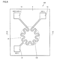
図5および図6を参照して、本発明に基づく実施の形態3における圧電デバイスについて説明する。図6は、図5におけるVI−VI線に関する矢視断面図である。Also in the present embodiment, the same effect as in the first embodiment can be obtained.
(Embodiment 3)
With reference to FIG. 5 and FIG. 6, the piezoelectric device in
本実施の形態における圧電デバイス103は、基本的な構成においては実施の形態1で説明した圧電デバイス101と同様である。ただし、以下の点で異なる。圧電デバイス103では、上部電極5とは別に圧電体層4の上側にヒータ6が配置されているのではなく、上部電極5がヒータ6を兼ねている。
The
上部電極5兼ヒータ6は、平面視したときに貫通孔8の外縁に沿うように配置されている。上部電極5兼ヒータ6は、平面視したときにミアンダ形状である。このような上部電極5であっても、下部電極3と対向していることによって、駆動電極および/または検出電極として機能しうる。下部電極3は、圧電体層4の全域に配置されていてもよいが、圧電体層4を挟んで上部電極5と対向するように、貫通孔8の内側において貫通孔8の外周部に沿うようなリング形状に配置されていてもよい。
The
本実施の形態においても、実施の形態1と同様の効果を得ることができる。上部電極5がヒータ6を兼ねていることによって、圧電デバイスの全体サイズの小型化を図ることも可能となる。
Also in the present embodiment, the same effect as in the first embodiment can be obtained. Since the
(実施の形態4)
図7および図8を参照して、本発明に基づく実施の形態4における圧電デバイスについて説明する。図8は、図7におけるVIII−VIII線に関する矢視断面図である。(Embodiment 4)
With reference to FIG. 7 and FIG. 8, the piezoelectric device in
本実施の形態における圧電デバイス104は、基本的な構成においては実施の形態3で説明した圧電デバイス103と同様である。ただし、以下の点で異なる。圧電デバイス103においては、上部電極5兼ヒータ6は、平面視したときに貫通孔8の外周部に沿うように配置されていたが、本実施の形態における圧電デバイス104においては、上部電極5兼ヒータ6は、平面視したときに貫通孔8の中央部に位置するように配置されている。上部電極5兼ヒータ6は、部分的にミアンダ形状となっている。このような上部電極5であっても、下部電極3と対向していることによって、駆動電極および/または検出電極として機能しうる。下部電極3は、圧電体層4の全域に配置されていてもよいが、圧電体層4を挟んで上部電極5と対向するように、貫通孔8の中央部において円形の部材として配置されていてもよい。
The
本実施の形態においても、実施の形態3と同様の効果を得ることができる。
(実施の形態5)
図9〜図11を参照して、本発明に基づく実施の形態5における圧電デバイスについて説明する。本実施の形態における圧電デバイス105の平面図を図9に示す。図10は、図9におけるX−X線に関する矢視断面図である。圧電デバイス105から圧電体層4および圧電体層4より上側に形成されたものを取り去った状態を図11に示す。図11においては、下部電極3より手前に存在するものは、二点鎖線で表示している。図11に示すように、円形の下部電極3が支持層2の上面に配置されている。Also in the present embodiment, the same effect as in the third embodiment can be obtained.
(Embodiment 5)
With reference to FIGS. 9 to 11, a piezoelectric device according to a fifth embodiment of the present invention will be described. FIG. 9 shows a plan view of the
本実施の形態における圧電デバイス105は、基本的な構成においては実施の形態4で説明した圧電デバイス104と同様である。ただし、以下の点で異なる。圧電デバイス104においては、上部電極5兼ヒータ6は、平面視したときに貫通孔8の中央部に位置するように配置されていたが、本実施の形態における圧電デバイス105においては、上部電極5兼ヒータ6は、平面視したときに貫通孔8のほぼ全体を占めるように配置されている。一方、下部電極3は、上部電極5兼ヒータ6の中央部に重なるように配置されている。すなわち、下部電極3は、メンブレン部7の中央部にのみ配置されている。下部電極3は円形となっている。
The
上部電極5兼ヒータ6は、部分的にミアンダ形状となっており、ミアンダ形状となっている部分が圧電体層4を挟んで下部電極3と対向している。
The
図9においては、説明の便宜のため、貫通孔8の形状線を上部電極5兼ヒータ6の外形線よりわずかに外側にずらして表示しているが、実際には両者は一致していてもよい。また、貫通孔8の外形線は、上部電極5兼ヒータ6の外形線より外側とは限らず内側に位置してもよい。
In FIG. 9, for convenience of explanation, the shape line of the through-
本実施の形態においても、実施の形態3と同様の効果を得ることができる。
(実施の形態6)
図12〜図14を参照して、本発明に基づく実施の形態6における圧電デバイスについて説明する。本実施の形態における圧電デバイス106の平面図を図12に示す。図13は、図12におけるXIII−XIII線に関する矢視断面図である。圧電デバイス106から圧電体層4および圧電体層4より上側に形成されたものを取り去った状態を図14に示す。図14においては、下部電極3より手前に存在するものは、二点鎖線で表示している。Also in the present embodiment, the same effect as in the third embodiment can be obtained.
(Embodiment 6)
With reference to FIGS. 12-14, the piezoelectric device in
本実施の形態における圧電デバイス106は、基本的な構成においては実施の形態5で説明した圧電デバイス105と同様である。ただし、以下の点で異なる。圧電デバイス105においては、下部電極3は、上部電極5兼ヒータ6の中央部に重なるように配置されていたが、圧電デバイス106においては、下部電極3は、上部電極5兼ヒータ6の外周部に重なるように配置されている。すなわち、下部電極3は、貫通孔8の内側において貫通孔8の外縁に沿うようなリング形状で配置されている。図14には下部電極3の形状がより明確に示されている。
The
本実施の形態においても、実施の形態5と同様の効果を得ることができる。
なお、今回開示した上記実施の形態はすべての点で例示であって制限的なものではない。本発明の範囲は上記した説明ではなくて請求の範囲によって示され、請求の範囲と均等の意味および範囲内でのすべての変更を含むものである。Also in the present embodiment, the same effect as in the fifth embodiment can be obtained.
In addition, the said embodiment disclosed this time is an illustration in all the points, Comprising: It is not restrictive. The scope of the present invention is defined by the terms of the claims, rather than the description above, and is intended to include any modifications within the scope and meaning equivalent to the terms of the claims.
本発明は、圧電デバイスに利用することができる。 The present invention can be used for a piezoelectric device.
1 基板、2 支持層、3 下部電極、4 圧電体層、5 上部電極、6 ヒータ、7 メンブレン部、8 貫通孔、11,12,13,14 電極、15 配線。 1 substrate, 2 support layer, 3 lower electrode, 4 piezoelectric layer, 5 upper electrode, 6 heater, 7 membrane part, 8 through-hole, 11, 12, 13, 14 electrode, 15 wiring.
Claims (8)
少なくとも一部が前記基板に重ならないメンブレン部となるように、前記基板によって直接または間接的に支持され、前記基板より上側に配置された圧電体層と、
少なくとも前記メンブレン部において前記圧電体層の下側に配置された下部電極と、
前記メンブレン部において前記圧電体層を挟んで前記下部電極の少なくとも一部に対向するように前記圧電体層の上側に配置された上部電極とを備え、
前記上部電極とは別に前記圧電体層の上側にヒータが配置されているか、または、前記上部電極の少なくとも一部がヒータを兼ねている、圧電デバイス。A substrate,
A piezoelectric layer that is directly or indirectly supported by the substrate and disposed above the substrate so that at least a portion thereof does not overlap the substrate;
A lower electrode disposed below the piezoelectric layer in at least the membrane part;
An upper electrode disposed on the upper side of the piezoelectric layer so as to face at least a part of the lower electrode across the piezoelectric layer in the membrane portion;
A piezoelectric device in which a heater is disposed above the piezoelectric layer separately from the upper electrode, or at least a part of the upper electrode also serves as a heater.
Applications Claiming Priority (3)
| Application Number | Priority Date | Filing Date | Title |
|---|---|---|---|
| JP2014121564 | 2014-06-12 | ||
| JP2014121564 | 2014-06-12 | ||
| PCT/JP2015/065591 WO2015190322A1 (en) | 2014-06-12 | 2015-05-29 | Piezoelectric device |
Publications (2)
| Publication Number | Publication Date |
|---|---|
| JPWO2015190322A1 JPWO2015190322A1 (en) | 2017-04-20 |
| JP6256605B2 true JP6256605B2 (en) | 2018-01-10 |
Family
ID=54833423
Family Applications (1)
| Application Number | Title | Priority Date | Filing Date |
|---|---|---|---|
| JP2016527744A Expired - Fee Related JP6256605B2 (en) | 2014-06-12 | 2015-05-29 | Piezoelectric device |
Country Status (3)
| Country | Link |
|---|---|
| US (1) | US10593860B2 (en) |
| JP (1) | JP6256605B2 (en) |
| WO (1) | WO2015190322A1 (en) |
Families Citing this family (6)
| Publication number | Priority date | Publication date | Assignee | Title |
|---|---|---|---|---|
| WO2016114173A1 (en) * | 2015-01-13 | 2016-07-21 | 株式会社村田製作所 | Method for manufacturing piezoelectric device |
| DE102017124256A1 (en) | 2016-10-29 | 2018-05-03 | Sendsor Gmbh | Sensor and method for measuring the properties of the respiratory gas |
| US10852261B2 (en) * | 2016-10-29 | 2020-12-01 | Sendsor Gmbh | Sensor and method for measuring respiratory gas properties |
| FR3070080B1 (en) * | 2017-08-09 | 2019-08-23 | Commissariat A L'energie Atomique Et Aux Energies Alternatives | METHOD FOR MANUFACTURING AN IMPACT LOCATION DEVICE HAVING AT LEAST THREE FIXED TRANSDUCERS AGAINST AN INTERACTIVE SURFACE |
| WO2020026611A1 (en) * | 2018-07-30 | 2020-02-06 | 株式会社村田製作所 | Piezoelectric device |
| KR102638990B1 (en) * | 2018-09-04 | 2024-02-22 | 현대자동차주식회사 | Micorphone, fabricating method for microphone, and control method for microphone |
Family Cites Families (11)
| Publication number | Priority date | Publication date | Assignee | Title |
|---|---|---|---|---|
| JPS62239800A (en) * | 1986-04-11 | 1987-10-20 | Matsushita Electric Works Ltd | Piezoelectric element |
| JPH10256570A (en) * | 1997-03-14 | 1998-09-25 | Matsushita Electric Ind Co Ltd | Thin film device and thin film manufacturing method |
| US6441539B1 (en) * | 1999-11-11 | 2002-08-27 | Murata Manufacturing Co., Ltd. | Piezoelectric resonator |
| US7400217B2 (en) * | 2003-10-30 | 2008-07-15 | Avago Technologies Wireless Ip Pte Ltd | Decoupled stacked bulk acoustic resonator band-pass filter with controllable pass bandwith |
| DE102005043039B4 (en) | 2005-09-09 | 2008-10-30 | Siemens Ag | Device with piezoacoustic resonator element, method for its production and method for outputting a signal as a function of a resonant frequency |
| JP2009260723A (en) | 2008-04-17 | 2009-11-05 | Asahi Kasei Electronics Co Ltd | Transducer |
| US10129656B2 (en) * | 2009-01-30 | 2018-11-13 | Avago Technologies International Sales Pte. Limited | Active temperature control of piezoelectric membrane-based micro-electromechanical devices |
| JP2011082624A (en) * | 2009-10-02 | 2011-04-21 | Asahi Kasei Electronics Co Ltd | Proximity ultrasonic sensor |
| US9490418B2 (en) * | 2011-03-29 | 2016-11-08 | Avago Technologies General Ip (Singapore) Pte. Ltd. | Acoustic resonator comprising collar and acoustic reflector with temperature compensating layer |
| US9240767B2 (en) * | 2012-05-31 | 2016-01-19 | Texas Instruments Incorporated | Temperature-controlled integrated piezoelectric resonator apparatus |
| US9401691B2 (en) * | 2014-04-30 | 2016-07-26 | Avago Technologies General Ip (Singapore) Pte. Ltd. | Acoustic resonator device with air-ring and temperature compensating layer |
-
2015
- 2015-05-29 JP JP2016527744A patent/JP6256605B2/en not_active Expired - Fee Related
- 2015-05-29 WO PCT/JP2015/065591 patent/WO2015190322A1/en active Application Filing
-
2016
- 2016-11-18 US US15/355,369 patent/US10593860B2/en not_active Expired - Fee Related
Also Published As
| Publication number | Publication date |
|---|---|
| US10593860B2 (en) | 2020-03-17 |
| JPWO2015190322A1 (en) | 2017-04-20 |
| WO2015190322A1 (en) | 2015-12-17 |
| US20170069821A1 (en) | 2017-03-09 |
Similar Documents
| Publication | Publication Date | Title |
|---|---|---|
| JP6256605B2 (en) | Piezoelectric device | |
| JP5576331B2 (en) | Pressure sensor device | |
| JP5605433B2 (en) | Piezoelectric vibration device | |
| JP6552644B2 (en) | Impedance matching layer for ultrasonic transducers with metallic protective structure | |
| JP2016518739A5 (en) | ||
| JP2013055573A5 (en) | ||
| JP2017173122A5 (en) | ||
| JP2007060465A5 (en) | ||
| JP7015484B2 (en) | MEMS device | |
| JP2008283618A5 (en) | ||
| JP4241245B2 (en) | Sensor device | |
| CN104760923B (en) | MEMS sensor | |
| JP2014074635A (en) | Ultrasonic sensor | |
| JP6429266B2 (en) | Electronic component equipment | |
| JP2014013735A (en) | Pressure switch | |
| JP2013113692A (en) | Infrared sensor | |
| JP2016152478A5 (en) | ||
| JP7173333B2 (en) | vibration device | |
| JP4816282B2 (en) | Actuator | |
| US20170363488A1 (en) | Protective electrode for a piezoceramic sensor | |
| JP2007248415A (en) | Pressure sensor element | |
| JP6692892B2 (en) | Acoustic sensor having a housing and a diaphragm element arranged in the housing | |
| US9690094B2 (en) | Optical device and manufacturing method thereof | |
| JP5447693B2 (en) | Acceleration sensor | |
| KR20200025203A (en) | Gas sensor and manufacturing method of the same |
Legal Events
| Date | Code | Title | Description |
|---|---|---|---|
| A521 | Request for written amendment filed |
Free format text: JAPANESE INTERMEDIATE CODE: A523 Effective date: 20161115 |
|
| A621 | Written request for application examination |
Free format text: JAPANESE INTERMEDIATE CODE: A621 Effective date: 20161115 |
|
| TRDD | Decision of grant or rejection written | ||
| A01 | Written decision to grant a patent or to grant a registration (utility model) |
Free format text: JAPANESE INTERMEDIATE CODE: A01 Effective date: 20171107 |
|
| A61 | First payment of annual fees (during grant procedure) |
Free format text: JAPANESE INTERMEDIATE CODE: A61 Effective date: 20171120 |
|
| R150 | Certificate of patent or registration of utility model |
Ref document number: 6256605 Country of ref document: JP Free format text: JAPANESE INTERMEDIATE CODE: R150 |
|
| LAPS | Cancellation because of no payment of annual fees |