JP6246414B2 - Semiconductor laser light source device, semiconductor laser light source system, and video display device - Google Patents
Semiconductor laser light source device, semiconductor laser light source system, and video display device Download PDFInfo
- Publication number
- JP6246414B2 JP6246414B2 JP2017500289A JP2017500289A JP6246414B2 JP 6246414 B2 JP6246414 B2 JP 6246414B2 JP 2017500289 A JP2017500289 A JP 2017500289A JP 2017500289 A JP2017500289 A JP 2017500289A JP 6246414 B2 JP6246414 B2 JP 6246414B2
- Authority
- JP
- Japan
- Prior art keywords
- semiconductor laser
- light source
- laser light
- cooler
- disposed
- Prior art date
- Legal status (The legal status is an assumption and is not a legal conclusion. Google has not performed a legal analysis and makes no representation as to the accuracy of the status listed.)
- Expired - Fee Related
Links
- 239000004065 semiconductor Substances 0.000 title claims description 234
- 239000000758 substrate Substances 0.000 claims description 32
- 230000017525 heat dissipation Effects 0.000 claims description 24
- 238000001816 cooling Methods 0.000 claims description 17
- 238000010586 diagram Methods 0.000 description 19
- 230000003287 optical effect Effects 0.000 description 5
- 230000005855 radiation Effects 0.000 description 5
- 239000011521 glass Substances 0.000 description 3
- 239000000428 dust Substances 0.000 description 2
- 230000000694 effects Effects 0.000 description 2
- 238000005286 illumination Methods 0.000 description 2
- 239000007788 liquid Substances 0.000 description 2
- 239000007787 solid Substances 0.000 description 2
- OAICVXFJPJFONN-UHFFFAOYSA-N Phosphorus Chemical compound [P] OAICVXFJPJFONN-UHFFFAOYSA-N 0.000 description 1
- 238000006243 chemical reaction Methods 0.000 description 1
- 230000006866 deterioration Effects 0.000 description 1
- 230000007613 environmental effect Effects 0.000 description 1
- 239000004973 liquid crystal related substance Substances 0.000 description 1
- 238000000034 method Methods 0.000 description 1
- NJPPVKZQTLUDBO-UHFFFAOYSA-N novaluron Chemical compound C1=C(Cl)C(OC(F)(F)C(OC(F)(F)F)F)=CC=C1NC(=O)NC(=O)C1=C(F)C=CC=C1F NJPPVKZQTLUDBO-UHFFFAOYSA-N 0.000 description 1
- 229910052710 silicon Inorganic materials 0.000 description 1
- 239000010703 silicon Substances 0.000 description 1
- XLYOFNOQVPJJNP-UHFFFAOYSA-N water Substances O XLYOFNOQVPJJNP-UHFFFAOYSA-N 0.000 description 1
Images


Classifications
-
- H—ELECTRICITY
- H01—ELECTRIC ELEMENTS
- H01S—DEVICES USING THE PROCESS OF LIGHT AMPLIFICATION BY STIMULATED EMISSION OF RADIATION [LASER] TO AMPLIFY OR GENERATE LIGHT; DEVICES USING STIMULATED EMISSION OF ELECTROMAGNETIC RADIATION IN WAVE RANGES OTHER THAN OPTICAL
- H01S5/00—Semiconductor lasers
- H01S5/02—Structural details or components not essential to laser action
- H01S5/024—Arrangements for thermal management
- H01S5/02407—Active cooling, e.g. the laser temperature is controlled by a thermo-electric cooler or water cooling
- H01S5/02423—Liquid cooling, e.g. a liquid cools a mount of the laser
-
- H—ELECTRICITY
- H01—ELECTRIC ELEMENTS
- H01S—DEVICES USING THE PROCESS OF LIGHT AMPLIFICATION BY STIMULATED EMISSION OF RADIATION [LASER] TO AMPLIFY OR GENERATE LIGHT; DEVICES USING STIMULATED EMISSION OF ELECTROMAGNETIC RADIATION IN WAVE RANGES OTHER THAN OPTICAL
- H01S5/00—Semiconductor lasers
- H01S5/02—Structural details or components not essential to laser action
- H01S5/022—Mountings; Housings
- H01S5/0239—Combinations of electrical or optical elements
-
- H—ELECTRICITY
- H01—ELECTRIC ELEMENTS
- H01S—DEVICES USING THE PROCESS OF LIGHT AMPLIFICATION BY STIMULATED EMISSION OF RADIATION [LASER] TO AMPLIFY OR GENERATE LIGHT; DEVICES USING STIMULATED EMISSION OF ELECTROMAGNETIC RADIATION IN WAVE RANGES OTHER THAN OPTICAL
- H01S5/00—Semiconductor lasers
- H01S5/02—Structural details or components not essential to laser action
- H01S5/024—Arrangements for thermal management
- H01S5/02407—Active cooling, e.g. the laser temperature is controlled by a thermo-electric cooler or water cooling
-
- H—ELECTRICITY
- H01—ELECTRIC ELEMENTS
- H01S—DEVICES USING THE PROCESS OF LIGHT AMPLIFICATION BY STIMULATED EMISSION OF RADIATION [LASER] TO AMPLIFY OR GENERATE LIGHT; DEVICES USING STIMULATED EMISSION OF ELECTROMAGNETIC RADIATION IN WAVE RANGES OTHER THAN OPTICAL
- H01S5/00—Semiconductor lasers
- H01S5/02—Structural details or components not essential to laser action
- H01S5/026—Monolithically integrated components, e.g. waveguides, monitoring photo-detectors, drivers
- H01S5/0261—Non-optical elements, e.g. laser driver components, heaters
-
- H—ELECTRICITY
- H01—ELECTRIC ELEMENTS
- H01S—DEVICES USING THE PROCESS OF LIGHT AMPLIFICATION BY STIMULATED EMISSION OF RADIATION [LASER] TO AMPLIFY OR GENERATE LIGHT; DEVICES USING STIMULATED EMISSION OF ELECTROMAGNETIC RADIATION IN WAVE RANGES OTHER THAN OPTICAL
- H01S5/00—Semiconductor lasers
- H01S5/40—Arrangement of two or more semiconductor lasers, not provided for in groups H01S5/02 - H01S5/30
- H01S5/4025—Array arrangements, e.g. constituted by discrete laser diodes or laser bar
- H01S5/4087—Array arrangements, e.g. constituted by discrete laser diodes or laser bar emitting more than one wavelength
- H01S5/4093—Red, green and blue [RGB] generated directly by laser action or by a combination of laser action with nonlinear frequency conversion
-
- H—ELECTRICITY
- H04—ELECTRIC COMMUNICATION TECHNIQUE
- H04N—PICTORIAL COMMUNICATION, e.g. TELEVISION
- H04N9/00—Details of colour television systems
- H04N9/12—Picture reproducers
- H04N9/31—Projection devices for colour picture display, e.g. using electronic spatial light modulators [ESLM]
- H04N9/3141—Constructional details thereof
- H04N9/3144—Cooling systems
-
- H—ELECTRICITY
- H04—ELECTRIC COMMUNICATION TECHNIQUE
- H04N—PICTORIAL COMMUNICATION, e.g. TELEVISION
- H04N9/00—Details of colour television systems
- H04N9/12—Picture reproducers
- H04N9/31—Projection devices for colour picture display, e.g. using electronic spatial light modulators [ESLM]
- H04N9/3141—Constructional details thereof
- H04N9/315—Modulator illumination systems
- H04N9/3161—Modulator illumination systems using laser light sources
-
- H—ELECTRICITY
- H04—ELECTRIC COMMUNICATION TECHNIQUE
- H04N—PICTORIAL COMMUNICATION, e.g. TELEVISION
- H04N9/00—Details of colour television systems
- H04N9/12—Picture reproducers
- H04N9/31—Projection devices for colour picture display, e.g. using electronic spatial light modulators [ESLM]
- H04N9/3141—Constructional details thereof
- H04N9/315—Modulator illumination systems
- H04N9/3164—Modulator illumination systems using multiple light sources
-
- H—ELECTRICITY
- H01—ELECTRIC ELEMENTS
- H01S—DEVICES USING THE PROCESS OF LIGHT AMPLIFICATION BY STIMULATED EMISSION OF RADIATION [LASER] TO AMPLIFY OR GENERATE LIGHT; DEVICES USING STIMULATED EMISSION OF ELECTROMAGNETIC RADIATION IN WAVE RANGES OTHER THAN OPTICAL
- H01S5/00—Semiconductor lasers
- H01S5/02—Structural details or components not essential to laser action
- H01S5/022—Mountings; Housings
- H01S5/02208—Mountings; Housings characterised by the shape of the housings
- H01S5/02212—Can-type, e.g. TO-CAN housings with emission along or parallel to symmetry axis
-
- H—ELECTRICITY
- H01—ELECTRIC ELEMENTS
- H01S—DEVICES USING THE PROCESS OF LIGHT AMPLIFICATION BY STIMULATED EMISSION OF RADIATION [LASER] TO AMPLIFY OR GENERATE LIGHT; DEVICES USING STIMULATED EMISSION OF ELECTROMAGNETIC RADIATION IN WAVE RANGES OTHER THAN OPTICAL
- H01S5/00—Semiconductor lasers
- H01S5/02—Structural details or components not essential to laser action
- H01S5/024—Arrangements for thermal management
- H01S5/02476—Heat spreaders, i.e. improving heat flow between laser chip and heat dissipating elements
-
- H—ELECTRICITY
- H01—ELECTRIC ELEMENTS
- H01S—DEVICES USING THE PROCESS OF LIGHT AMPLIFICATION BY STIMULATED EMISSION OF RADIATION [LASER] TO AMPLIFY OR GENERATE LIGHT; DEVICES USING STIMULATED EMISSION OF ELECTROMAGNETIC RADIATION IN WAVE RANGES OTHER THAN OPTICAL
- H01S5/00—Semiconductor lasers
- H01S5/40—Arrangement of two or more semiconductor lasers, not provided for in groups H01S5/02 - H01S5/30
- H01S5/4025—Array arrangements, e.g. constituted by discrete laser diodes or laser bar
Landscapes
- Physics & Mathematics (AREA)
- Optics & Photonics (AREA)
- Condensed Matter Physics & Semiconductors (AREA)
- General Physics & Mathematics (AREA)
- Electromagnetism (AREA)
- Engineering & Computer Science (AREA)
- Multimedia (AREA)
- Signal Processing (AREA)
- Projection Apparatus (AREA)
- Semiconductor Lasers (AREA)
- Non-Portable Lighting Devices Or Systems Thereof (AREA)
Description
本発明は、半導体レーザを冷却する冷却器を備える半導体レーザ光源装置および半導体レーザ光源システムと、半導体レーザ光源装置または半導体レーザ光源システムを備える映像表示装置に関するものである。 The present invention relates to a semiconductor laser light source device and a semiconductor laser light source system including a cooler for cooling a semiconductor laser, and an image display device including the semiconductor laser light source device or the semiconductor laser light source system.
近年、大ホールまたはデジタルシネマ向けの大型高輝度プロジェクタ、主に少人数の会議またはプレゼンテーションに用いられる中小型プロジェクタ、および筐体に投射光学系と大型スクリーンを内蔵するプロジェクションモニタなどに用いられる光源として、LEDまたは半導体レーザ等の固体光源を使用するものが広く商品化、または提案がなされている。これらの機器においては、従来の多くのプロジェクタおよびプロジェクションモニタの光源として使用されてきたランプに対して、固体光源を使用することで一層広い色再現範囲を持つ、瞬時点灯が可能である、低消費電力である、および長寿命であるなどの利点を持つことを特徴とする。 As a light source used in large halls and large-scale high-intensity projectors for digital cinema in recent years, medium- and small-sized projectors mainly used for meetings or presentations with a small number of people, and projection monitors with a built-in projection optical system and a large screen. Those using solid-state light sources such as LEDs or semiconductor lasers have been widely commercialized or proposed. In these devices, compared to the lamps that have been used as the light source of many conventional projectors and projection monitors, a solid color light source can be used for instant lighting and low power consumption. It is characterized by having advantages such as electric power and long life.
特に半導体レーザには、光を重畳させることで更なる高輝度化、および高出力化が可能となる利点も併せ持つ。そのため、大画面への投射に用いられる大型高輝度プロジェクタ用途として、より多数の半導体レーザを用いた高出力半導体レーザ光源装置の開発が進められている。 In particular, a semiconductor laser has an advantage that higher brightness and higher output can be achieved by superimposing light. Therefore, development of a high-power semiconductor laser light source device using a larger number of semiconductor lasers has been advanced as a large-sized high-intensity projector used for projection onto a large screen.
しかし、半導体レーザは、LEDなど他の固体光源と比較して熱に弱く、素子の温度が上昇するに従い、電気−光変換効率が著しく低下しやすい。また、高温状態で高出力の光を出射し続けると劣化が促進し、素子の寿命も短くなりやすい。そのため、環境温度が高温時にも所望の光量を得るためには、他の個体光源よりも冷却性能の高い放熱構造が必要になる。 However, semiconductor lasers are less susceptible to heat than other solid-state light sources such as LEDs, and the electro-optical conversion efficiency is likely to decrease significantly as the temperature of the element increases. Further, if high-power light is continuously emitted at a high temperature, deterioration is promoted and the life of the device is likely to be shortened. Therefore, in order to obtain a desired light amount even when the environmental temperature is high, a heat dissipation structure with higher cooling performance than other solid light sources is required.
例えば、特許文献1には、複数の半導体レーザを放熱するため、半導体レーザを取り付けた台座に複数の短径波状の放熱フィンを設けて、冷却ファンを放熱フィンに対して複数の穴を設けたドライバ基板を挟んで配置した構造が開示されている。
For example, in
また、特許文献2には、半導体レーザと半導体レーザを電気的に接続するフレキシブル基板を、伝熱部材またはヒートシンクの基部に埋設して、半導体レーザを放熱する構造が開示されている。
特許文献1に記載の構造では、複数の半導体レーザを冷却するために形成した放熱フィンは、複数の穴を設けたドライバ基板を介して、冷却ファンによって冷却されている。ドライバ基板が冷却ファンの風を遮るため、放熱フィンを効率よく冷却することができず、冷却性能が低下し、半導体レーザを効率よく冷却することができないという問題点があった。
In the structure described in
特許文献2に記載の構造では、半導体レーザとヒートシンクとの間に電気的に接続するフレキシブル基板を配置すると、発熱源である半導体レーザとヒートシンクとの間の接触面積が減るため、熱抵抗が増加して冷却性能が低下し、半導体レーザを効率よく冷却することができないという問題点があった。
In the structure described in
そこで、本発明は、半導体レーザを効率よく冷却することが可能な技術を提供することを目的とする。 Accordingly, an object of the present invention is to provide a technique capable of efficiently cooling a semiconductor laser.
本発明に係る半導体レーザ光源装置は、半導体レーザと、半導体レーザを冷却する冷却器と、前記半導体レーザを駆動する駆動基板とを備え、前記冷却器は、前記半導体レーザの出射面とは反対側の面と接するように配置され、前記駆動基板は、前記冷却器における前記半導体レーザが配置される側の面とは反対側の面と接するように配置され、前記冷却器の内部に空洞が設けられ、前記空洞に複数のフィンが配置されるものである。 A semiconductor laser light source device according to the present invention includes a semiconductor laser, a cooler that cools the semiconductor laser, and a drive substrate that drives the semiconductor laser, and the cooler is opposite to the emission surface of the semiconductor laser. The drive substrate is disposed so as to be in contact with a surface of the cooler opposite to the surface on which the semiconductor laser is disposed, and a cavity is provided in the cooler. is, a plurality of fins in said cavity is shall be disposed.
本発明に係る別の半導体レーザ光源装置は、半導体レーザと、半導体レーザを冷却する冷却器と、前記半導体レーザを駆動する駆動基板とを備え、前記冷却器および前記駆動基板はそれぞれ、前記半導体レーザの出射面とは反対側の面と接するように配置され、前記冷却器は、幅方向中央部分が端部よりも高い高さ位置となる凸部状、または幅方向中央部分が端部よりも低い高さ位置となる凹部状に形成され、前記冷却器の下面に複数のフィンが配置されるものである。
Another semiconductor laser light source device according to the present invention includes a semiconductor laser, a cooler that cools the semiconductor laser, and a drive substrate that drives the semiconductor laser, and each of the cooler and the drive substrate includes the semiconductor laser. The cooler is disposed so as to contact the surface opposite to the exit surface of the projection, and the cooler has a convex shape in which the central portion in the width direction is at a height position higher than the end portion, or the central portion in the width direction is in contact with the end portion. it is formed in a recess shape having a low height, a plurality of fins on the lower surface of the cooler is shall be disposed.
本発明に係る半導体レーザ光源システムは、半導体レーザ光源装置を複数備えるものである。 The semiconductor laser light source system according to the present invention includes a plurality of semiconductor laser light source devices.
本発明に係る映像表示装置は、半導体レーザ光源装置または半導体レーザ光源システムを備えるものである。 The video display device according to the present invention includes a semiconductor laser light source device or a semiconductor laser light source system.
本発明によれば、半導体レーザと冷却器とを直接接触させるため、半導体レーザと冷却器との間の熱抵抗を低減でき、半導体レーザを効率よく冷却することができる。 According to the present invention, since the semiconductor laser and the cooler are brought into direct contact, the thermal resistance between the semiconductor laser and the cooler can be reduced, and the semiconductor laser can be efficiently cooled.
この発明の目的、特徴、局面、および利点は、以下の詳細な説明と添付図面とによって、より明白となる。 The objects, features, aspects and advantages of the present invention will become more apparent from the following detailed description and the accompanying drawings.
<実施の形態1>
本発明の実施の形態1について、図面を用いて以下に説明する。実施の形態1に係る半導体レーザ光源装置100、半導体レーザ光源システム200および映像表示装置300について詳細に説明するが、最初に映像表示装置300について説明する。図1は、実施の形態1に係る映像表示装置300の構成図である。<
映像表示装置300は、赤、青、緑の3種類の半導体レーザ光源装置100、照明光学系101、映像表示システム102および投射光学系103を備えている。ここで、半導体レーザ光源装置100とは、複数の半導体レーザを備える高出力半導体レーザ光源装置である。
The
赤、青、緑の半導体レーザ光源装置100からの出射光は、照明光学系101で合成されて白色の光に変換され、映像表示システム102に照射される。映像表示システム102として、DMD(Digital Light Processing)またはLCOS(Liquid Crystal On Silicon)などを用いることができる。映像表示システム102で作成された映像は、投射光学系103によって拡大されて、スクリーン104に表示される。
Light emitted from the red, blue, and green semiconductor laser
なお、図1に示す映像表示装置300は、赤、青、緑の3種類の半導体レーザ光源装置100を組み合わせて白色を表示するプロジェクタを想定したものであるが、半導体レーザと蛍光体を組み合わせて白色を表示、または半導体レーザとLEDを組み合わせて白色を表示する映像表示装置であってもよい。
The
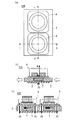
次に、実施の形態1に係る半導体レーザ光源装置100について説明する。図2は、半導体レーザ光源装置100の構成概要を示す図である。より具体的には、図2(a)は、半導体レーザ光源装置100の平面図であり、図2(b)は、図2(a)のA-A断面図であり、図2(c)は、半導体レーザ光源装置100の側面図である。図3は、半導体レーザ1の構成を示す図である。より具体的には、図3(a)は、半導体レーザ1の平面図であり、図3(b)は、図3(a)のB-B線断面図であり、図3(c)は、図3(a)のC-C線断面図である。
Next, the semiconductor laser
図2(a),(b),(c)に示すように、半導体レーザ光源装置100は、複数(例えば8つ)の半導体レーザ1、冷却器2および駆動基板3を備えている。先ず、半導体レーザ1について説明する。
As shown in FIGS. 2A, 2 </ b> B, and 2 </ b> C, the semiconductor laser
図3(a),(b),(c)に示すように、半導体レーザ1は、チップ11、発光層12、放熱ブロック13、プレート14、端子ピン15、CAN16およびガラス窓17を備えている。発光層12は、光を出射する層であり、チップ11に形成されている。チップ11は発熱するため、放熱ブロック13の側面に配置された状態でプレート14上に配置され、チップ11は放熱ブロック13に放熱している。端子ピン15は、外部から電力を供給して、チップ11に導通し、発光させるための部材であり、ワイヤ18を介してチップ11と接続されている。チップ11は、粉塵などの影響を受けて性能が劣化するため、放熱ブロック13を介してプレート14上に配置された状態でCAN16によって封止されている。これにより、粉塵などの影響を排除している。ガラス窓17は、CAN16の上面に配置され、発光層12からの出射光を透過する。なお、出射光は図中において矢印で示されており、他の図面においても同様である。
As shown in FIGS. 3A, 3 </ b> B, and 3 </ b> C, the
図2(a),(b),(c)に示すように、冷却器2は、半導体レーザ1を冷却する部材である。半導体レーザ1は、チップ11が配置された放熱ブロック13が正対するように2列に冷却器2の上面に配置されている。冷却器2は、半導体レーザ1の下面(半導体レーザ1の出射面とは反対側の面)と接するように配置され、また、放熱ブロック13の直下に配置されている。駆動基板3は、半導体レーザ1を駆動する駆動回路が搭載された基板である。駆動基板3は、冷却器2の下面(冷却器2における半導体レーザ1が配置される側の面とは反対側の面)と接するように配置されている。
As shown in FIGS. 2A, 2 </ b> B, and 2 </ b> C, the
冷却器2には、複数のフィン7が配置される空洞2aと、端子ピン15が挿通される複数の貫通穴2bが形成されている。空洞2aは、冷却器2の幅方向中央部において長手方向に沿って形成されており、放熱ブロック13の下側に位置し、放熱ブロック13の下側に複数のフィン7が配置されている。フィン7を流路として水などを流すことで、冷却器2は液冷装置として機能する。なお、流路は図中において白抜き矢印で示されており、他の図面においても同様である。
The
複数の貫通穴2bは、各半導体レーザ1の端子ピン15に対応する位置にそれぞれ形成されている。なお、図示しないが、駆動基板3にも端子ピン15が挿通される複数の貫通穴が形成されている。
The plurality of through
次に、半導体レーザ光源システム200について説明する。図4は、半導体レーザ光源システム200の構成概要を示す図である。図4に示すように、半導体レーザ光源システム200は、複数(例えば3つ)の半導体レーザ光源装置100を水平方向に並べて構成されている。なお、図4では、半導体レーザ光源装置100は個別に冷却器2を備える構成が示されているが、1つの冷却器2に3つの半導体レーザ光源装置100の半導体レーザ1を配置した構成であってもよい。また、図1に示す映像表示装置300は、3つの半導体レーザ光源装置100を備えているが、これに代えて3つの半導体レーザ光源システム200を備えていてもよい。
Next, the semiconductor laser
以上のように、実施の形態1に係る半導体レーザ光源装置100では、冷却器2は、半導体レーザ1の出射面とは反対側の面と接するように配置され、駆動基板3は、冷却器2における半導体レーザ1が配置される側の面とは反対側の面と接するように配置される。
As described above, in the semiconductor laser
したがって、半導体レーザ1と冷却器2とを直接接触させるため、半導体レーザ1と冷却器2との間の熱抵抗を低減でき、半導体レーザ1を効率よく冷却することができる。半導体レーザ1を効率よく冷却することで、半導体レーザ1ひいては半導体レーザ光源装置100の長期使用が可能となる。
Therefore, since the
また、半導体レーザ光源システム200は、半導体レーザ光源装置100を複数備えるため、半導体レーザ光源装置100単体よりも高出力化を図ることができる。
In addition, since the semiconductor laser
また、映像表示装置300は、半導体レーザ光源装置100を備えるため、半導体レーザ1を効率よく冷却することができる。または、映像表示装置300が半導体レーザ光源システム200を備える場合、上記の効果に加えて、半導体レーザ光源装置100を備える場合よりも高出力化を図ることができるという効果が得られる。
Further, since the
<実施の形態2>
次に、実施の形態2に係る半導体レーザ光源装置110について説明する。図5は、実施の形態2に係る半導体レーザ光源装置110の構成概要を示す図である。より具体的には、図5(a)は、半導体レーザ光源装置110の平面図であり、図5(b)は、図5(a)のE-E断面図であり、図5(c)は、半導体レーザ光源装置110のF-F断面図である。図6は、半導体素子4の構成を示す図である。より具体的には、図6(a)は、半導体素子4の平面図であり、図6(b)は、図6(a)のG-G断面図であり、図6(c)は、図6(a)のH-H断面図である。なお、実施の形態2において、実施の形態1で説明したものと同一の構成要素については同一符号を付して説明は省略する。<
Next, the semiconductor laser
図5(a),(b),(c)に示すように、半導体レーザ光源装置110は、半導体素子4、冷却器2および駆動基板3を備えている。図6(a),(b),(c)に示すように、半導体素子4は、放熱ブロック13に複数(例えば2つ)のチップ11を配置した大型の半導体素子である。半導体素子4は、複数(例えば2つ)のチップ11、複数(例えば14個)の発光層12、複数(例えば2つ)の放熱ブロック13、プレート14、端子ピン15、CAN16およびガラス窓17を備えている。半導体素子4は冷却器2の上面に配置され、各半導体素子4の2つの放熱ブロック13は互いに正対するように配置されている。
As shown in FIGS. 5A, 5 </ b> B, and 5 </ b> C, the semiconductor laser
1つのチップ11につき7つの発光層12が配置され、各半導体素子4において、2つの放熱ブロック13は、一方の放熱ブロック13に配置された7つの発光層12と、他方の放熱ブロック13に配置された7つの発光層12が互いに正対するように配置されている。発光層12の配置方向は、冷却器2の幅方向と平行である。また、2つの半導体素子4の配置方向は、発光層12の配置方向と垂直である。このため、フィン7の流路は、冷却器2の長手方向、すなわち、2つの半導体素子4の配置方向と平行となる。
Seven light emitting
半導体素子4のチップ11は、複数の発光層12を有するため、実施の形態1における半導体レーザ1の場合よりも大型になる。また、チップ11を冷却する放熱ブロック13およびプレート14も同様に大型になる。冷却器2は、放熱ブロック13の直下に半導体素子4と接するように配置されている。
Since the
端子ピン15は、放熱ブロック13の外側に配置されている。その結果、2つの放熱ブロック13を近接して配置することができる。また、端子ピン15を放熱ブロック13の外側に配置することで、冷却器2を、実施の形態1の場合と同様に半導体素子4に接した状態で、放熱ブロック13の直下に配置することができるようになる。その結果、放熱ブロック13と冷却器2との間の熱抵抗を低減することができるため、効率よく半導体素子4を冷却することができる。
The
さらに、半導体レーザ光源装置110は、複数の発光層12を有するチップ11を配置した半導体素子4を備えることで、実施の形態1における半導体レーザ1の場合と比較して、端子ピン15の本数を減らすことができるため、相対的に放熱面積を多くとることができる。これにより、半導体素子4を効率よく冷却することができる。
Furthermore, the semiconductor laser
次に、実施の形態2における他の構成について説明する。図7は、実施の形態2に係る半導体レーザ光源装置の他の構成概要を示す図である。より具体的には、図7(a)は、半導体レーザ光源装置120の平面図であり、図7(b)は、図7(a)のI-I線断面図であり、図7(c)は、図7(a)のJ-J線断面図である。
Next, another configuration in the second embodiment will be described. FIG. 7 is a diagram illustrating another configuration outline of the semiconductor laser light source device according to the second embodiment. More specifically, FIG. 7A is a plan view of the semiconductor laser
図5(a),(b),(c)の構成では、2つの半導体素子4の配置方向は、発光層12の配置方向と垂直である。その結果、1つの半導体素子4に対して、1つの流路を形成することができる。これに対して、図7(a),(b),(c)の構成では、2つの半導体素子4の配置方向は、発光層12の配置方向と平行である。すなわち、半導体素子4は、7つの発光層12の配置方向が冷却器2の長手方向と平行となるように配置されている。このため、フィン7の流路は冷却器2の幅方向と平行に形成され、流路が複数の半導体素子4を通過しないため、複数の半導体素子4の温度を個別に制御できるという効果が得られる。
5A, 5B, and 5C, the arrangement direction of the two
次に、実施の形態2に係る半導体レーザ光源システム201について説明する。図8は、半導体レーザ光源システム201の構成概要を示す図である。図8に示すように、半導体レーザ光源システム201は、複数(例えば3つ)の半導体レーザ光源装置110を水平方向に並べて構成されている。なお、図8では、半導体レーザ光源装置110は個別に冷却器2を備える構成が示されているが、1つの冷却器2に3つの半導体レーザ光源装置110の半導体素子4を配置した構成であってもよい。
Next, the semiconductor laser
また、半導体レーザ光源システム201は、複数の半導体レーザ光源装置110に代えて複数の半導体レーザ光源装置120を水平方向に並べて構成されてもよい。また、図1に示す映像表示装置300は、3つの半導体レーザ光源装置100を備えているが、これに代えて3つの半導体レーザ光源システム201を備えていてもよい。
The semiconductor laser
以上のように、実施の形態2に係る半導体レーザ光源装置110,120では、半導体レーザは、放熱ブロック13に複数のチップ11を配置した半導体素子4であり、冷却器2は、放熱ブロック13の直下に半導体素子4と接するように配置される。したがって、実施の形態1の場合と比較して端子ピン15の本数が減少するため、冷却器2と半導体素子4との接触面積が増加し、半導体素子4を一層効率よく冷却することができる。
As described above, in the semiconductor laser
このように、実施の形態1の場合と比較して端子ピン15の本数が減少するため、半導体レーザ光源装置110,120の小型化を図ることができる。
Thus, since the number of
半導体レーザ光源システム201は、半導体レーザ光源装置110または半導体レーザ光源装置120を複数備えるため、半導体レーザ光源装置110または半導体レーザ光源装置120単体よりも高出力化を図ることができる。
Since the semiconductor laser
また、光源自体を小型にすることができるため、信頼性が高く小型の映像表示装置300が得られる。
In addition, since the light source itself can be reduced in size, a small
<実施の形態3>
次に、実施の形態3に係る半導体レーザ光源装置130について説明する。図9は、実施の形態3に係る半導体レーザ光源装置130の構成概要を示す図である。より具体的には、図9(a)は、半導体レーザ光源装置130の平面図であり、図9(b)は、図9(a)のK-K線断面図であり、図9(c)は、半導体レーザ光源装置130の側面図である。なお、実施の形態3において、実施の形態1,2で説明したものと同一の構成要素については同一符号を付して説明は省略する。<
Next, the semiconductor laser
実施の形態1では、駆動基板3は、冷却器2の下面(冷却器2における半導体レーザ1が配置される側の面とは反対側の面)と接するように配置されたが、実施の形態3では、冷却器2および駆動基板3はそれぞれ、半導体レーザ1の出射面とは反対側の面と接するように配置されている。
In the first embodiment, the
図9(a),(b),(c)に示すように、半導体レーザ1は、放熱ブロック13が互いに正対するように2列に配置されている。冷却器2は、幅方向中央部分が端部よりも高い高さ位置となる凸部状に形成され、幅方向中央部分の上面が半導体レーザ1のプレート14の下面の内側部分と接するように配置されている。駆動基板3は、2つに分割され、プレート14の下面の外側部分とそれぞれ接するように配置されている。駆動基板3は、冷却器2の幅方向両端部の上側に配置され、冷却器2とは接していない。端子ピン15は、一対の駆動基板3から下方に突出するように配置されている。すなわち、端子ピン15は、半導体レーザ光源装置130の幅方向両端部に配置され、冷却器2は、半導体レーザ光源装置130の幅方向両端部に配置された端子ピン15の間に配置されている。
As shown in FIGS. 9A, 9B, and 9C, the
実施の形態3における冷却器2は、実施の形態1の場合と異なり、空洞2aと貫通穴2bを備えておらず、冷却器2の下面に複数のフィン7が配置されている。また、フィン7の背面にはファン8が配置されている。
Unlike the case of the first embodiment, the
次に、実施の形態3に係る半導体レーザ光源装置の他の構成概要について説明する。図10は、実施の形態3に係る半導体レーザ光源装置の他の構成概要を示す図である。より具体的には、図10(a)は、半導体レーザ光源装置140の平面図であり、図10(b)は、図10(a)のL-L断面図であり、図10(c)は、半導体レーザ光源装置140の側面図である。
Next, another configuration outline of the semiconductor laser light source device according to
図10(a),(b),(c)に示すように、半導体レーザ1は、発光層12を有するチップ11が正対するように2列に配置されている。端子ピン15は、半導体レーザ光源装置130の幅方向中央部分に配置されている。駆動基板3は、半導体レーザ光源装置130の幅方向中央部分に配置され、駆動基板3の幅方向両端部の上面が半導体レーザ1のプレート14の下面の内側部分と接するように配置されている。冷却器2は、幅方向中央部分が端部よりも低い高さ位置となる凹部状に形成され、幅方向両端部の上面が半導体レーザ1のプレート14の下面の外側部分と接するように配置されている。
As shown in FIGS. 10A, 10B, and 10C, the
次に、実施の形態3に係る半導体レーザ光源装置の他の構成概要として半導体素子4を備える場合について2つの構成概要を説明する。図11は、実施の形態3に係る半導体レーザ光源装置の他の構成概要を示す図である。より具体的には、図11(a)は、半導体レーザ光源装置150の平面図であり、図11(b)は、図11(a)のM-M断面図であり、図11(c)は、図11(a)のN-N断面図である。
Next, two configuration outlines will be described in the case where the
図11(a),(b),(c)に示すように、半導体レーザ光源装置150は、放熱ブロック13の外側に端子ピン15を配置した半導体素子4を備え、端子ピン15の間に冷却器2が配置された構成である。すなわち、図9(a),(b),(c)に示した半導体レーザ光源装置130において半導体レーザ1の代わりに半導体素子4を配置した例である。
As shown in FIGS. 11A, 11 </ b> B, and 11 </ b> C, the semiconductor laser
より具体的には、冷却器2は、幅方向中央部分が端部よりも高い高さ位置となる凸部状に形成され、幅方向中央部分の上面が半導体素子4のプレート14の下面の中央部分と接するように配置されている。駆動基板3は、2つに分割され、プレート14の下面の両端部分とそれぞれ接するように配置されている。駆動基板3は、冷却器2の幅方向両端部の上側に配置され、冷却器2とは接していない。
More specifically, the
次に、他方の構成概要について説明する。図12は、実施の形態3に係る半導体レーザ光源装置の他の構成概要を示す図である。より具体的には、図12(a)は、半導体レーザ光源装置160の平面図であり、図12(b)は、図12(a)のO-O断面図であり、図12(c)は、図12(a)のP-P断面図である。
Next, the other configuration outline will be described. FIG. 12 is a diagram illustrating another configuration outline of the semiconductor laser light source device according to the third embodiment. More specifically, FIG. 12 (a) is a plan view of the semiconductor laser
図12(a),(b),(c)に示すように、半導体レーザ光源装置160は、放熱ブロック13の外側の一方に端子ピン15を配置した半導体素子4を備え、放熱ブロック13の直下に冷却器2が配置され、端子ピン15の外側に駆動基板3が配置された構成である。
As shown in FIGS. 12A, 12B, and 12C, the semiconductor laser
より具体的には、冷却器2は、幅方向中央部分および一方の端部が他方の端部よりも高い高さ位置となる形状に形成され、幅方向中央部分および一方の端部の上面が半導体素子4のプレート14の下面の中央部分および一方の端部と接するように配置されている。駆動基板3は、プレート14の下面の他方の端部と接するように配置されている。駆動基板3は、冷却器2における幅方向の他方の端部の上側に配置され、冷却器2とは接していない。
More specifically, the
以上のように、実施の形態3に係る半導体レーザ光源装置130,140,150,160では、冷却器2および駆動基板3はそれぞれ、半導体レーザ1または半導体素子4の出射面とは反対側の面と接するように配置される。したがって、半導体レーザ1または半導体素子4と冷却器2とを直接接触させるため、半導体レーザ1または半導体素子4と冷却器2との間の熱抵抗を低減でき、半導体レーザ1または半導体素子4を効率よく冷却することができる。
As described above, in the semiconductor laser
実施の形態3では、冷却器2のフィン7の高さ位置を高くすることができるため、放熱面積を増加することができ、冷却器2の性能を向上させることができる。また、フィン7を冷却器2の外側に配置したため、フィン7の背面にファン8を配置した強制空冷の冷却器を構成することが可能となる。なお、実施の形態3では、ファン8を使用した強制空冷の冷却器2を示したが、実施の形態1,2の場合のように、強制空冷の代わりに液冷装置を配置することも可能である。
In
また、実施の形態1,2の場合と同様に、実施の形態3に係る半導体レーザ光源装置を半導体レーザ光源システムおよび映像表示装置に採用することが可能である。 Similarly to the first and second embodiments, the semiconductor laser light source device according to the third embodiment can be employed in the semiconductor laser light source system and the video display device.
この発明は詳細に説明されたが、上記した説明は、すべての局面において、例示であって、この発明がそれに限定されるものではない。例示されていない無数の変形例が、この発明の範囲から外れることなく想定され得るものと解される。 Although the present invention has been described in detail, the above description is illustrative in all aspects, and the present invention is not limited thereto. It is understood that countless variations that are not illustrated can be envisaged without departing from the scope of the present invention.
なお、本発明は、その発明の範囲内において、各実施の形態を自由に組み合わせたり、各実施の形態を適宜、変形、省略することが可能である。 It should be noted that the present invention can be freely combined with each other within the scope of the invention, and each embodiment can be appropriately modified or omitted.
1 半導体レーザ、2 冷却器、3 駆動基板、4 半導体素子、100,110,120,130,140,150,160 半導体レーザ光源装置、200,201 半導体レーザ光源システム、300 映像表示装置。
DESCRIPTION OF
Claims (9)
半導体レーザ(1)を冷却する冷却器(2)と、
前記半導体レーザ(1)を駆動する駆動基板(3)と、
を備え、
前記冷却器(2)は、前記半導体レーザ(1)の出射面とは反対側の面と接するように配置され、
前記駆動基板(3)は、前記冷却器(2)における前記半導体レーザ(1)が配置される側の面とは反対側の面と接するように配置され、
前記冷却器(2)の内部に空洞(2a)が設けられ、
前記空洞(2a)に複数のフィン(7)が配置される、半導体レーザ光源装置。 A semiconductor laser (1);
A cooler (2) for cooling the semiconductor laser (1);
A drive substrate (3) for driving the semiconductor laser (1);
With
The cooler (2) is disposed so as to be in contact with a surface opposite to the emission surface of the semiconductor laser (1),
The drive substrate (3) is disposed so as to be in contact with a surface opposite to the surface on which the semiconductor laser (1) is disposed in the cooler (2) ,
A cavity (2a) is provided inside the cooler (2),
It said cavity (2a) a plurality of fins (7) of Ru is disposed, a semiconductor laser light source device.
前記冷却器(2)は、前記放熱ブロック(13)の直下に前記半導体素子(4)と接するように配置される、請求項1記載の半導体レーザ光源装置。 The semiconductor laser (1) is a semiconductor element (4) in which a plurality of chips (11) are arranged on a heat dissipation block (13).
The semiconductor laser light source device according to claim 1, wherein the cooler (2) is disposed so as to be in contact with the semiconductor element (4) immediately below the heat dissipation block (13).
半導体レーザ(1)を冷却する冷却器(2)と、
前記半導体レーザ(1)を駆動する駆動基板(3)と、
を備え、
前記冷却器(2)および前記駆動基板(3)はそれぞれ、前記半導体レーザ(1)の出射面とは反対側の面と接するように配置され、
前記冷却器(2)は、幅方向中央部分が端部よりも高い高さ位置となる凸部状、または幅方向中央部分が端部よりも低い高さ位置となる凹部状に形成され、
前記冷却器(2)の下面に複数のフィン(7)が配置される、半導体レーザ光源装置。 A semiconductor laser (1);
A cooler (2) for cooling the semiconductor laser (1);
A drive substrate (3) for driving the semiconductor laser (1);
With
Each of the cooler (2) and the drive substrate (3) is disposed so as to be in contact with a surface opposite to the emission surface of the semiconductor laser (1) ,
The cooler (2) is formed in a convex shape in which the central portion in the width direction is at a height position higher than the end portion, or a concave shape in which the central portion in the width direction is at a height position lower than the end portion,
Wherein the plurality of fins on the lower surface of the cooler (2) (7) Ru is disposed, a semiconductor laser light source device.
Applications Claiming Priority (3)
| Application Number | Priority Date | Filing Date | Title |
|---|---|---|---|
| JP2015027218 | 2015-02-16 | ||
| JP2015027218 | 2015-02-16 | ||
| PCT/JP2015/083458 WO2016132622A1 (en) | 2015-02-16 | 2015-11-27 | Semiconductor laser light source device, semiconductor laser light source system, and image display device |
Publications (2)
| Publication Number | Publication Date |
|---|---|
| JPWO2016132622A1 JPWO2016132622A1 (en) | 2017-06-08 |
| JP6246414B2 true JP6246414B2 (en) | 2017-12-13 |
Family
ID=56692632
Family Applications (1)
| Application Number | Title | Priority Date | Filing Date |
|---|---|---|---|
| JP2017500289A Expired - Fee Related JP6246414B2 (en) | 2015-02-16 | 2015-11-27 | Semiconductor laser light source device, semiconductor laser light source system, and video display device |
Country Status (6)
| Country | Link |
|---|---|
| US (1) | US9899795B2 (en) |
| EP (1) | EP3261197B1 (en) |
| JP (1) | JP6246414B2 (en) |
| CN (1) | CN107210582B (en) |
| CA (1) | CA2979520C (en) |
| WO (1) | WO2016132622A1 (en) |
Families Citing this family (3)
| Publication number | Priority date | Publication date | Assignee | Title |
|---|---|---|---|---|
| DE112017007585B4 (en) * | 2017-05-24 | 2022-09-08 | Mitsubishi Electric Corporation | semiconductor assembly |
| JP7014645B2 (en) * | 2018-03-06 | 2022-02-01 | シャープ株式会社 | Semiconductor light emitting device |
| JP6667149B1 (en) * | 2019-02-06 | 2020-03-18 | ウシオ電機株式会社 | Semiconductor laser light source device |
Family Cites Families (22)
| Publication number | Priority date | Publication date | Assignee | Title |
|---|---|---|---|---|
| US5900967A (en) * | 1996-12-12 | 1999-05-04 | Trw Inc. | Laser diode mounting technique to evenly deposit energy |
| JP2001326411A (en) | 2000-05-12 | 2001-11-22 | Hitachi Koki Co Ltd | Semiconductor laser device |
| JP2003188456A (en) * | 2001-12-19 | 2003-07-04 | Hitachi Ltd | Photoelectronic device |
| JP2004128044A (en) * | 2002-09-30 | 2004-04-22 | Toshiba Corp | Semiconductor laser device |
| JP4662526B2 (en) | 2003-07-29 | 2011-03-30 | セイコーインスツル株式会社 | Laser diode module |
| US20060097385A1 (en) * | 2004-10-25 | 2006-05-11 | Negley Gerald H | Solid metal block semiconductor light emitting device mounting substrates and packages including cavities and heat sinks, and methods of packaging same |
| JP4929612B2 (en) * | 2005-04-12 | 2012-05-09 | ソニー株式会社 | Semiconductor laser device and heat sink |
| JP2007127398A (en) * | 2005-10-05 | 2007-05-24 | Seiko Epson Corp | Heat exchanger, heat exchanger manufacturing method, liquid cooling system, light source device, projector, electronic device unit, electronic equipment |
| JP5435854B2 (en) * | 2007-10-13 | 2014-03-05 | 日亜化学工業株式会社 | Semiconductor light emitting device |
| CN101960681B (en) * | 2008-03-18 | 2012-05-30 | 三菱电机株式会社 | Laser light source module |
| WO2010090766A1 (en) * | 2009-02-09 | 2010-08-12 | Jan Vetrovec | Heat transfer device |
| JP5500339B2 (en) | 2009-09-29 | 2014-05-21 | カシオ計算機株式会社 | Light source device and projector |
| US8018980B2 (en) * | 2010-01-25 | 2011-09-13 | Lawrence Livermore National Security, Llc | Laser diode package with enhanced cooling |
| US20120177076A1 (en) * | 2010-01-27 | 2012-07-12 | Mitsubishi Electric Corporation | Semiconductor laser module |
| CN102237632A (en) * | 2010-04-26 | 2011-11-09 | 无锡亮源激光技术有限公司 | Outdoor semiconductor laser module |
| CN101854027A (en) * | 2010-04-30 | 2010-10-06 | 西安炬光科技有限公司 | Liquid refrigerator for semiconductor laser |
| JP5910508B2 (en) | 2011-01-07 | 2016-04-27 | 日本電気株式会社 | Laser light source module |
| CN103875139A (en) * | 2011-11-16 | 2014-06-18 | 三菱电机株式会社 | Semiconductor laser-excitation solid-state laser |
| JP2013149667A (en) * | 2012-01-17 | 2013-08-01 | Sumitomo Electric Device Innovations Inc | Optical module and optical transmitter |
| JP2014003062A (en) * | 2012-06-15 | 2014-01-09 | Mitsubishi Electric Corp | Optical semiconductor device |
| JP2014138148A (en) * | 2013-01-18 | 2014-07-28 | Hitachi Media Electoronics Co Ltd | Semiconductor laser, semiconductor laser array and image display device |
| US20140270731A1 (en) * | 2013-03-12 | 2014-09-18 | Applied Materials, Inc. | Thermal management apparatus for solid state light source arrays |
-
2015
- 2015-11-27 WO PCT/JP2015/083458 patent/WO2016132622A1/en active Application Filing
- 2015-11-27 JP JP2017500289A patent/JP6246414B2/en not_active Expired - Fee Related
- 2015-11-27 CN CN201580073348.6A patent/CN107210582B/en not_active Expired - Fee Related
- 2015-11-27 CA CA2979520A patent/CA2979520C/en active Active
- 2015-11-27 EP EP15882723.8A patent/EP3261197B1/en active Active
- 2015-11-27 US US15/527,219 patent/US9899795B2/en not_active Expired - Fee Related
Also Published As
| Publication number | Publication date |
|---|---|
| EP3261197B1 (en) | 2021-06-30 |
| EP3261197A1 (en) | 2017-12-27 |
| WO2016132622A1 (en) | 2016-08-25 |
| CA2979520A1 (en) | 2016-08-25 |
| US20170353003A1 (en) | 2017-12-07 |
| EP3261197A4 (en) | 2018-11-21 |
| US9899795B2 (en) | 2018-02-20 |
| CA2979520C (en) | 2020-12-01 |
| JPWO2016132622A1 (en) | 2017-06-08 |
| CN107210582B (en) | 2020-04-03 |
| CN107210582A (en) | 2017-09-26 |
Similar Documents
| Publication | Publication Date | Title |
|---|---|---|
| US7309145B2 (en) | Light source apparatus and projection display apparatus | |
| JP5511420B2 (en) | Laser light source device and projector device | |
| TWI459123B (en) | Cooling apparatus of porjector | |
| US20060250270A1 (en) | System and method for mounting a light emitting diode to a printed circuit board | |
| CN112083624B (en) | Electronic device and projection device provided with same | |
| JP5556256B2 (en) | Illumination device and projection-type image display device | |
| JP2011075898A (en) | Projector | |
| TWM447998U (en) | Mini optical image device | |
| TW201430478A (en) | Cooling apparatus of projector | |
| TWM552113U (en) | Projector device and heat dissipation system thereof | |
| TWM467084U (en) | Mini optical image device | |
| JP6246414B2 (en) | Semiconductor laser light source device, semiconductor laser light source system, and video display device | |
| JP4654664B2 (en) | Light source device and projection display device | |
| US9389496B2 (en) | Projector with cooling unit | |
| JP2007103748A (en) | Heat exchanger, liquid cooling system, light source device, projector, electronic device unit, electronic equipment | |
| JP2007133300A (en) | Semiconductor light source device and projection type video display device using same | |
| JP6593901B2 (en) | Light source device, projection display device, and method for cooling semiconductor light emitting element | |
| JP2004333757A (en) | Light source device and projection display device using the same | |
| JP4345507B2 (en) | Light source device and projector | |
| JP6725118B2 (en) | Light source device, projection display device, and semiconductor light emitting element cooling method | |
| JP2005202112A (en) | Light source device and projection display device | |
| JP6079409B2 (en) | Liquid crystal display | |
| JP2017138353A (en) | Backlight light source and liquid crystal display device | |
| JP2015060137A (en) | Optical module and projection type image display device | |
| WO2018042519A1 (en) | Light source apparatus, light source system, and projection-type display apparatus |
Legal Events
| Date | Code | Title | Description |
|---|---|---|---|
| A521 | Request for written amendment filed |
Free format text: JAPANESE INTERMEDIATE CODE: A523 Effective date: 20170208 |
|
| A621 | Written request for application examination |
Free format text: JAPANESE INTERMEDIATE CODE: A621 Effective date: 20170208 |
|
| TRDD | Decision of grant or rejection written | ||
| A01 | Written decision to grant a patent or to grant a registration (utility model) |
Free format text: JAPANESE INTERMEDIATE CODE: A01 Effective date: 20171017 |
|
| A61 | First payment of annual fees (during grant procedure) |
Free format text: JAPANESE INTERMEDIATE CODE: A61 Effective date: 20171114 |
|
| R150 | Certificate of patent or registration of utility model |
Ref document number: 6246414 Country of ref document: JP Free format text: JAPANESE INTERMEDIATE CODE: R150 |
|
| R250 | Receipt of annual fees |
Free format text: JAPANESE INTERMEDIATE CODE: R250 |
|
| LAPS | Cancellation because of no payment of annual fees |