JP6236635B2 - Solid-state imaging device and driving method thereof - Google Patents
Solid-state imaging device and driving method thereof Download PDFInfo
- Publication number
- JP6236635B2 JP6236635B2 JP2014549763A JP2014549763A JP6236635B2 JP 6236635 B2 JP6236635 B2 JP 6236635B2 JP 2014549763 A JP2014549763 A JP 2014549763A JP 2014549763 A JP2014549763 A JP 2014549763A JP 6236635 B2 JP6236635 B2 JP 6236635B2
- Authority
- JP
- Japan
- Prior art keywords
- reset transistor
- reset
- potential
- solid
- imaging device
- Prior art date
- Legal status (The legal status is an assumption and is not a legal conclusion. Google has not performed a legal analysis and makes no representation as to the accuracy of the status listed.)
- Active
Links
Images


Classifications
-
- H—ELECTRICITY
- H04—ELECTRIC COMMUNICATION TECHNIQUE
- H04N—PICTORIAL COMMUNICATION, e.g. TELEVISION
- H04N25/00—Circuitry of solid-state image sensors [SSIS]; Control thereof
- H04N25/60—Noise processing, e.g. detecting, correcting, reducing or removing noise
- H04N25/65—Noise processing, e.g. detecting, correcting, reducing or removing noise applied to reset noise, e.g. KTC noise related to CMOS structures by techniques other than CDS
-
- H—ELECTRICITY
- H04—ELECTRIC COMMUNICATION TECHNIQUE
- H04N—PICTORIAL COMMUNICATION, e.g. TELEVISION
- H04N25/00—Circuitry of solid-state image sensors [SSIS]; Control thereof
- H04N25/70—SSIS architectures; Circuits associated therewith
- H04N25/71—Charge-coupled device [CCD] sensors; Charge-transfer registers specially adapted for CCD sensors
- H04N25/75—Circuitry for providing, modifying or processing image signals from the pixel array
-
- H—ELECTRICITY
- H04—ELECTRIC COMMUNICATION TECHNIQUE
- H04N—PICTORIAL COMMUNICATION, e.g. TELEVISION
- H04N25/00—Circuitry of solid-state image sensors [SSIS]; Control thereof
- H04N25/70—SSIS architectures; Circuits associated therewith
- H04N25/76—Addressed sensors, e.g. MOS or CMOS sensors
- H04N25/767—Horizontal readout lines, multiplexers or registers
-
- H—ELECTRICITY
- H04—ELECTRIC COMMUNICATION TECHNIQUE
- H04N—PICTORIAL COMMUNICATION, e.g. TELEVISION
- H04N25/00—Circuitry of solid-state image sensors [SSIS]; Control thereof
- H04N25/70—SSIS architectures; Circuits associated therewith
- H04N25/76—Addressed sensors, e.g. MOS or CMOS sensors
- H04N25/77—Pixel circuitry, e.g. memories, A/D converters, pixel amplifiers, shared circuits or shared components
-
- H—ELECTRICITY
- H04—ELECTRIC COMMUNICATION TECHNIQUE
- H04N—PICTORIAL COMMUNICATION, e.g. TELEVISION
- H04N25/00—Circuitry of solid-state image sensors [SSIS]; Control thereof
- H04N25/70—SSIS architectures; Circuits associated therewith
- H04N25/76—Addressed sensors, e.g. MOS or CMOS sensors
- H04N25/78—Readout circuits for addressed sensors, e.g. output amplifiers or A/D converters
Landscapes
- Engineering & Computer Science (AREA)
- Multimedia (AREA)
- Signal Processing (AREA)
- Solid State Image Pick-Up Elements (AREA)
- Transforming Light Signals Into Electric Signals (AREA)
Description
本発明は、固体撮像装置に関し、特に積層型の固体撮像装置およびその駆動方法に関する。 The present invention relates to a solid-state imaging device, and more particularly to a stacked solid-state imaging device and a driving method thereof.
積層型の固体撮像装置の例として、特許文献1がある。この積層型の固体撮像装置では、制御電極の上に光電変換膜が形成され、この光電変換膜の上に透明電極層が形成される。積層型の固体撮像装置は、この透明電極に印加した電圧の作用を、光電変換膜を介して制御電極に及ぼすことにより良好なSN比で光情報を電気信号に変えることができる。
There exists
積層型の固体撮像装置は、画素回路が形成された半導体基板の上に絶縁膜を介して光電変換膜が形成された構成を有している。このため、光電変換膜にアモルファスシリコン等の光吸収係数が大きい材料を用いることが可能となる。 A stacked solid-state imaging device has a configuration in which a photoelectric conversion film is formed on a semiconductor substrate on which a pixel circuit is formed via an insulating film. For this reason, it is possible to use a material having a large light absorption coefficient such as amorphous silicon for the photoelectric conversion film.
しかしながら、特許文献1に示された固体撮像装置は、信号電荷をリセットするときに雑音が発生する。すなわち、特許文献1に示された固体撮像装置は、リセット信号に含まれるリセットパルスの後縁(後ろ側のエッジ)に起因して、リセット信号線と画素電極等との間の容量結合によりランダムノイズ(リセット雑音)が発生してしまうという問題を有している。積層型の固体撮像装置は、電荷の完全転送ができないために、一般的な埋め込みフォトダイオード型の固体撮像装置のように、CDS(相関二重サンプリング)回路でサンプリングを実施しても、リセット雑音(kTCノイズ)のキャンセルが不完全になる。これにより、雑音が発生した状態において、リセット後の電荷に次の信号電荷が加算されるためにリセット雑音が重畳された信号電荷が読み出される。このため、特許文献1に示された固体撮像装置は、ランダム雑音が大きくなるという問題を有している。
However, the solid-state imaging device disclosed in
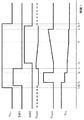
kTCノイズを低減するため、特許文献2のような技術が提案されている。特許文献2に開示された隣接4画素の画素部とその周辺回路を図14に示す。31a〜31dの点線で囲われた領域は各画素を表す。37a〜37dはリセットトランジスタであり、43a〜43dは選択トランジスタである。また、端子40a、40bは、選択トランジスタのゲートに電圧を印加するための端子である。端子45a、45bは、リセットトランジスタのゲートに電圧を印加するための端子である。蓄積部に蓄えられた電荷の電荷排出動作は、選択された行の各画素内のリセットトランジスタを完全にオンした後、オフすることによってなされる。読出しトランジスタからの読出し信号は垂直信号線を介して、各列に配置されている負帰還増幅器33a、33bに入力され、その出力信号はリセットトランジスタのソースに帰還される。リセットトランジスタが完全にオン状態にあるとき、ノイズ信号がノイズ源である電荷蓄積部に負帰還することにより、ノイズをキャンセルすることを目的とした構成である。
In order to reduce kTC noise, a technique such as
特許文献2に開示された技術は、電荷排出時すなわちリセットトランジスタが導通状態(完全にオンまたは弱反転でオン)にあるときにのみ、逆相のノイズ信号加算されることによってキャンセルされる。このとき、リセットトランジスタがオフになるに従い、回路全体の帯域が狭くなり、周波数の高いノイズのキャンセルに遅延が発生する。すなわち、特許文献に開示された技術には、リセット動作に長時間が必要となる、という課題があった。
The technique disclosed in
上記課題を鑑み、本発明は、ノイズキャンセルに必要な時間を大幅に短縮することができる固体撮像装置とその駆動方法を提供することを目的とする。 In view of the above problems, an object of the present invention is to provide a solid-state imaging device and a driving method thereof that can significantly reduce the time required for noise cancellation.
上記課題を解決するために、固体撮像装置は、光電変換部と、光電変換部で生じた信号電荷を読み出すための回路であって、光電変換部と電気的に接続された電荷蓄積部と、ソースまたはドレインの一方が電荷蓄積部と電気的に接続されたリセットトランジスタとを含む、信号読み出し回路と、信号読み出し回路の出力を、リセットトランジスタのソースまたはドレインの他方に負帰還させる負帰還回路とを備え、電荷蓄積部に蓄積された電荷を排出するリセット動作は、負帰還回路がオフ状態である第1の期間と、第1の期間の後であって、負帰還回路がオン状態である第2の期間とを含み、第1の期間において、リセットトランジスタがオフ状態からオン状態へ変化した後、再びオフ状態となり、第2の期間において、リセットトランジスタを徐々にオン状態へと変化させるリセットトランジスタ制御電圧が印加されることを特徴とする。 In order to solve the above problems, a solid-state imaging device includes a photoelectric conversion unit, a circuit for reading signal charges generated in the photoelectric conversion unit, a charge storage unit electrically connected to the photoelectric conversion unit, A signal readout circuit including a reset transistor in which one of the source and the drain is electrically connected to the charge storage unit; and a negative feedback circuit for negatively feeding back the output of the signal readout circuit to the other of the source and the drain of the reset transistor; The reset operation for discharging the charge accumulated in the charge accumulating unit is after the first period when the negative feedback circuit is in the off state and after the first period, and the negative feedback circuit is in the on state Including a second period. In the first period, the reset transistor changes from the off state to the on state and then turns off again. In the second period, the reset transistor Wherein the reset transistor control voltage that changes gradually to turn on the motor is applied.
更に、好ましくは、第2の期間の初期において、電荷蓄積部の電位が第1の電位となり、リセットトランジスタのソースまたはドレインの他方の電位が第2の電位となり、リセットトランジスタがNMOSトランジスタである場合、第2の電位が第1の電位よりも低い値に設定され、リセットトランジスタがPMOSトランジスタの場合、第2の電位が第1の電位よりも高い値に設定される。 Further preferably, in the initial stage of the second period, the potential of the charge storage portion becomes the first potential, the other potential of the source or drain of the reset transistor becomes the second potential, and the reset transistor is an NMOS transistor. When the second potential is set to a value lower than the first potential and the reset transistor is a PMOS transistor, the second potential is set to a value higher than the first potential.
更に、好ましくは、リセットレベル発生回路をさらに備え、第1の期間においてリセットトランジスタがオン状態のとき、リセットレベル発生回路がリセットトランジスタのソースまたはドレインの他方に接続される。 Furthermore, it is preferable to further include a reset level generation circuit, and when the reset transistor is in an ON state in the first period, the reset level generation circuit is connected to the other of the source and the drain of the reset transistor.
更に、好ましくは、テーパ波形発生回路をさらに備え、第2の期間において、テーパ波形発生回路より、リセットトランジスタ制御電圧が出力される。 Further, preferably, a taper waveform generation circuit is further provided, and a reset transistor control voltage is output from the taper waveform generation circuit in the second period.
実施形態では、リセットトランジスタ制御電圧は、リセットトランジスタのゲートに入力される。 In the embodiment, the reset transistor control voltage is input to the gate of the reset transistor.
実施形態では、リセットトランジスタ制御電圧は、負帰還回路の出力に重畳される。 In the embodiment, the reset transistor control voltage is superimposed on the output of the negative feedback circuit.
実施形態では、負帰還回路は二つの入力端子を有し、信号読み出し回路の出力が第1の入力端子に入力され、参照電圧が第2の入力端子に入力され、リセットトランジスタ制御電圧は、負帰還回路の第2の入力端子に入力される。 In the embodiment, the negative feedback circuit has two input terminals, the output of the signal readout circuit is input to the first input terminal, the reference voltage is input to the second input terminal, and the reset transistor control voltage is negative. It is input to the second input terminal of the feedback circuit.
実施形態では、リセットトランジスタ制御電圧の印加時に、リセットトランジスタのチャネルを弱反転状態とする電圧が、リセットトランジスタのゲートに入力される。 In the embodiment, when the reset transistor control voltage is applied, a voltage that causes the channel of the reset transistor to be in a weakly inverted state is input to the gate of the reset transistor.
実施形態では、リセットトランジスタ制御電圧の印加時に、リセットトランジスタの電荷蓄積部側はオフ状態であり、負帰還回路側は弱反転状態にバイアスされる。 In the embodiment, when the reset transistor control voltage is applied, the charge storage unit side of the reset transistor is in an off state, and the negative feedback circuit side is biased to a weak inversion state.
また、固体撮像装置の駆動方法は、光電変換部と、光電変換部で生じた信号電荷を読み出すための回路であって、光電変換部と電気的に接続された電荷蓄積部と、ソースまたはドレインの一方が電荷蓄積部と電気的に接続されたリセットトランジスタとを含む、信号読み出し回路と、信号読み出し回路の出力を、リセットトランジスタのソースまたはドレインの他方に負帰還させる負帰還回路とを備えた固体撮像装置の駆動方法であって、負帰還回路をオフ状態とし、リセットトランジスタをオフ状態からオン状態へ変化させた後、再びオフ状態とする第1のリセット動作と、第1のリセット動作の後に、負帰還回路をオン状態とし、リセットトランジスタを徐々にオン状態へと変化させるリセットトランジスタ制御電圧を印加する第2のリセット動作とを有することを特徴とする。 The solid-state imaging device is driven by a photoelectric conversion unit, a circuit for reading signal charges generated in the photoelectric conversion unit, a charge storage unit electrically connected to the photoelectric conversion unit, and a source or drain Including a reset transistor electrically connected to the charge storage portion, and a negative feedback circuit for negatively feeding back the output of the signal read circuit to the other of the source and drain of the reset transistor A method for driving a solid-state imaging device, wherein a first feedback operation in which a negative feedback circuit is turned off, a reset transistor is changed from an off state to an on state, and then turned off again, and a first reset operation is performed. Later, a second feedback circuit is applied to apply a reset transistor control voltage that turns on the negative feedback circuit and gradually changes the reset transistor to the on state. And having a Tsu preparative operation.
本開示の固体撮像装置によれば、ノイズキャンセルに必要な時間を大幅に短縮することができる固体撮像装置とその駆動方法を提供することができる。 According to the solid-state imaging device of the present disclosure, it is possible to provide a solid-state imaging device and a driving method thereof that can significantly reduce the time required for noise cancellation.
以下、本発明に係る固体撮像装置およびその駆動方法の実施形態について、図面を参照しながら説明する。なお、本発明について、以下の実施形態及び添付の図面を用いて説明を行うが、これは例示を目的としており、本発明がこれらの実施形態に限定されることを意図しない。 Embodiments of a solid-state imaging device and a driving method thereof according to the present invention will be described below with reference to the drawings. In addition, although this invention is demonstrated using the following embodiment and accompanying drawing, this is for the purpose of illustration and this invention is not intended to be limited to these embodiment.
(第1の実施形態)
まず、第1の実施形態に係る固体撮像装置の全体構成を説明する。図1は、第1の実施形態に係る固体撮像装置101の構成を示すブロック図である。(First embodiment)
First, the overall configuration of the solid-state imaging device according to the first embodiment will be described. FIG. 1 is a block diagram illustrating a configuration of a solid-
この固体撮像装置101は、複数の画素110からなる画素アレイ102と、行信号駆動回路103a及び103bと、列毎に配置された列回路104と、各列に配置された相関二重サンプリング(CDS)回路などのノイズキャンセラ回路105と、水平駆動回路106と、出力段アンプ107と、センサ出力108とを備える。
The solid-
回路109はテーパ波形発生回路であり、この回路で発生した信号は、行信号駆動回路103a及び103bを介して、各行のリセット時に各画素のリセットトランジスタに供給される。
A
図2は、固体撮像装置101の3画素分の領域の断面図である。なお、実際の画素は、画素アレイ102内に、例えば1000万画素分配列されている。各画素の回路図は後述する。
FIG. 2 is a cross-sectional view of a region corresponding to three pixels of the solid-
図2に示すように、固体撮像装置101は、マイクロレンズ201と、青色カラーフィルタ202と、緑色カラーフィルタ203と、赤色カラーフィルタ204と、保護膜205と、平坦化膜206と、上部電極207と、光電変換膜208と、電子ブロッキング層209と、電極間絶縁膜210と、下部電極211と、配線間絶縁膜212と、給電層213と、配線層214と、基板218と、基板218内に形成されたウェル219と、STI(Shallow Trench Isolation)分離領域220と、層間絶縁層221とを備える。なお、分離領域220はSTIに限らず、注入分離であってもよい。
As shown in FIG. 2, the solid-
基板218は、半導体基板であり、例えばシリコン基板である。基板218内のウェル219には、光電変換膜208の光電変換により生成された信号電荷を信号電圧(読み出し信号)として画素外部に読み出すための信号読み出し回路を構成する、複数のトランジスタが形成されている。複数のトランジスタには、増幅トランジスタ216、選択トランジスタ(図示せず)及びリセットトランジスタ217が含まれる。
The
マイクロレンズ201は、入射光を効率よく集光するために、固体撮像装置101の最表面に、画素110ごとに形成されている。
The
青色カラーフィルタ202、緑色カラーフィルタ203及び赤色カラーフィルタ204は、カラー画像を撮像するために形成されている。また、青色カラーフィルタ202、緑色カラーフィルタ203及び赤色カラーフィルタ204は、各マイクロレンズ201の直下、かつ保護膜205内に形成されている。1000万画素分にわたって集光ムラ及び色ムラのないマイクロレンズ201及びカラーフィルタ群を形成するために、これらの光学素子は平坦化膜206上に形成されている。平坦化膜206は、例えば、SiNで構成される。
The
上部電極207は、平坦化膜206下に画素アレイ102の全面にわたって形成されている。この上部電極207は可視光を透過する。例えば、上部電極207はITO(Indium Tin Oxide)で構成される。
The
光電変換膜208は光を信号電荷に変換する。具体的には、光電変換膜208は、上部電極207の下に形成されており、高い光吸収能を有する有機分子で構成されている。また、光電変換膜208の厚さは、例えば500nmである。また、光電変換膜208は、真空蒸着法を用いて形成される。上記有機分子は波長400nmから700nmの可視光全域にわたって高い光吸収能を有する。
The
電子ブロッキング層209は、光電変換膜208の下に形成されており、入射光の光電変換によって発生した正孔を伝導するとともに、下部電極211からの電子注入を阻止する。この電子ブロッキング層209は、高い平坦度を有する電極間絶縁膜210と下部電極211上に形成されている。
The
複数の下部電極211は、基板218の上方に、行列状に配置されている。また、複数の下部電極211は、各々が電気的に分離されている。具体的には、下部電極211は、電極間絶縁膜210間に形成されており、光電変換膜208で発生した正孔を収集する。この下部電極211は、例えばTiNで構成される。また、下部電極211は、平坦化された厚さ100nmの配線間絶縁膜212上に形成されている。
The plurality of
また、各下部電極211は0.2μmの間隔で分離されている。そして、この分離領域にも電極間絶縁膜210が埋め込まれている。
The
さらに、この分離領域の下方、かつ配線間絶縁膜212下に給電層213が配されている。この給電層213は、例えばCuで構成される。具体的には、給電層213は、隣接する下部電極211の間の領域であり、かつ下部電極211と基板218との間に形成されている。また、給電層213には、下部電極211とは独立した電位を供給可能である。具体的には、光電変換膜208が光電変換を行う露光動作時、及び信号読み出し回路が読み出し信号を生成する読み出し動作時に、給電層213に、信号電荷を排斥するための電位が供給される。例えば、信号電荷が正孔の場合には正電圧が印加される。これにより、各画素に、隣接画素から正孔が混入することを防止できる。なお、このような電圧印加の制御は、例えば、固体撮像装置101が備える制御部(図示せず)により行なわれる。下部電極211には配線層214が電気的に接続されている。
Further, a
なお、図2に示す画素の構造は、好ましい例を示すものであり、本発明は上述したような画素の構造に限定されるものではない。 Note that the pixel structure shown in FIG. 2 is a preferable example, and the present invention is not limited to the pixel structure described above.
次に、本実施形態の信号読み出し回路の構成をより詳細に説明する。配線層214は、信号読み出し回路のFD部(電荷蓄積部)215及び増幅トランジスタ216のゲート端子に接続されている。FD部215は、リセットトランジスタ217のソースまたはドレインとなる拡散領域の一方と電気的に接続される。ここで、FD部と、リセットトランジスタとは、拡散領域を共有している。なお、FD部とリセットトランジスタのソースまたはドレインとなる拡散領域とが別に形成され、互いに電気的に接続されていてもよい。リセットトランジスタと、増幅トランジスタと、選択トランジスタ(図示せず)と、FD部215とは、全て同一のP型のウェル219内に形成されている。また、このウェル219は、基板218に形成されている。つまり、信号読み出し回路は、基板218に形成されており、複数の下部電極211の各々に発生する電流又は電圧の変化を検知することにより、信号電荷に応じた読み出し信号を生成する。また、増幅トランジスタ216は、下部電極211に発生する電流又は電圧の変化を増幅することにより、読み出し信号を生成する。
Next, the configuration of the signal readout circuit of this embodiment will be described in more detail. The
また、各トランジスタは、STI分離領域220によって電気的に分離されている。
Each transistor is electrically isolated by the
また、リセットトランジスタ217のゲート端子はリセットトランジスタ制御線(図示せず)と接続され、リセットトランジスタ制御線の電位によりリセットトランジスタ217のオン・オフが制御されている。例えば、リセットトランジスタ制御線の電位がハイレベルとされていると、リセットトランジスタ217がオンされ、リセットトランジスタ制御線の電位がローレベルとされていると、リセットトランジスタ217がオフされる。
The gate terminal of the
また、選択トランジスタのゲート端子は選択トランジスタ制御線(図示せず)と接続され、選択トランジスタ制御線の電位により選択トランジスタのオン・オフが制御されている。例えば、選択トランジスタ制御線の電位がハイレベルとされていると、選択トランジスタがオンされ、選択トランジスタ制御線の電位がローレベルとされていると、選択トランジスタがオフされる。 The gate terminal of the selection transistor is connected to a selection transistor control line (not shown), and the on / off state of the selection transistor is controlled by the potential of the selection transistor control line. For example, when the potential of the selection transistor control line is high level, the selection transistor is turned on, and when the potential of the selection transistor control line is low level, the selection transistor is turned off.
図3は、本実施形態における、画素アレイ102のm(mは自然数)行n(nは自然数)列に属する画素110の回路およびその制御回路の一例を表した図である。画素110は、光電変換部301と、光電変換部で生じた信号電荷を読み出すための回路である信号読み出し回路とを備え、信号読み出し回路は、FD部215と、増幅トランジスタ216と、選択トランジスタ302と、リセットトランジスタ217とを有する。光電変換部301は、上部電極207と、光電変換膜208と、電子ブロッキング層209と、下部電極211とを有し、入射光を光電変換することにより、入射光量に応じた信号電荷を生成する。なお、このとき上部電極207は、所定のバイアスレベルVMにバイアスされている。選択トランジスタ302のソースまたはドレインの一方が増幅トランジスタ216のソースまたはドレインの一方に接続されており、選択トランジスタ302のソースまたはドレインの他方が列信号線303に接続されている。増幅トランジスタ216のソースまたはドレインの他方は、電源(図示せず)に接続されている。選択トランジスタ302は、増幅トランジスタ216で検出された信号を列信号線303へ伝達するか否かを制御する。列信号線303は列信号線の分岐点304で分岐し、一つの経路はフィードバックアンプ305の入力端子に接続されており、もう一方の経路は列信号読み出し回路306に接続されている。フィードバックアンプ305は二つの入力端子を有する差動アンプであり、列信号線303が接続される入力端子とは別の入力端子には、参照電圧レベルVREFが入力されている。フィードバックアンプ305の出力は列信号線307に接続され、スイッチ(SW2)309を介してリセットトランジスタ217のソースまたはドレインの他方、すなわち、FD部とは反対側に接続されている。フィードバックアンプ305により、信号読み出し回路の出力を、リセットトランジスタのソースまたはドレインの他方に負帰還させる負帰還回路が形成されている。なお、負帰還回路は二入力の差動アンプに限られず、信号読み出し回路の出力を負帰還できる回路であればよい。また、リセットトランジスタ217のソースまたはドレインの他方はスイッチ(SW1)308を介してリセットレベル発生回路310にも接続されている。前述の通り、リセットトランジスタ217のソースまたはドレインの一方は、FD部215に接続されている。リセットトランジスタ217のゲートは行信号駆動回路103a及び103bから出力された行信号線311に接続されている。行信号駆動回路103aおよび103bはテーパ波形発生回路109からの信号の出力バッファ回路312を含み、その出力は行信号線311に接続されている。フィードバックアンプ305は列回路104に含まれ、列信号読み出し回路306は、ノイズキャンセラ回路105に含まれる。テーパ波形発生回路109、リセットレベル発生回路310は、固体撮像装置101と同一チップ内に設けられていても良く、別チップ内に設けられていても良い。FIG. 3 is a diagram illustrating an example of a circuit of the
なお、本実施形態では、画素110を構成するトランジスタはNMOSトランジスタであるとしたが、この極性は反転しても良い。すなわち、画素110を構成するトランジスタがPMOSトランジスタであっても良い。
In the present embodiment, the transistors constituting the
図4は、図3に示した画素110を含むm行目の画素およびその制御回路の駆動方法を示したタイミングチャートである。時刻t1において選択トランジスタ302のゲートをハイレベルとし、当該画素を含む行全体の画素を選択する。時刻t2においてスイッチ(SW1)308をオン状態に設定し、リセットトランジスタ217のソースまたはドレインの他方をリセットレベル発生回路310の信号に接続し、初期電圧VRST1に設定する。時刻t1とt2の間にFD部215に蓄積されていた画像信号を読み出す。
FIG. 4 is a timing chart showing a driving method of the m-th row pixel including the
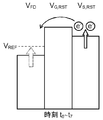
t2以後に、FD部に蓄積された電荷を排出するリセット動作が行われる。リセット動作は、負帰還回路がオフ状態である第1の期間と、第1の期間の後であって、負帰還回路がオン状態である第2の期間とを含む。本実施形態においては、スイッチ(SW2)309のオン・オフにより負帰還回路のオン・オフが制御されており、スイッチ(SW2)309がオフ状態であるときに負帰還回路がオフ状態となり、スイッチ(SW2)309がオン状態であるときに負帰還回路がオン状態となる。時刻t3においてリセットトランジスタ217のゲートをハイレベルに設定し、リセットトランジスタ217をオフ状態からオン状態へと変化させ、FD部をリセットレベル発生回路出力レベルにリセットする。以降、このリセット動作をプリリセットと称する。時刻t4において、リセットトランジスタ217を再びオフ状態とし、プリリセット動作を終了する。このとき、FD部はフローティングとなり、リセットトランジスタ217のゲート−ドレイン間の寄生容量の影響により、FD部に僅かな電圧変動が起こる。時刻t5においてSW1をオフ状態として、リセットレベル発生回路310を切り離す。このとき、SW1がオフ状態となることにより、リセットトランジスタ217のソースまたはドレインの他方はフローティングとなる。プリリセット動作により、FD部215は、平均的には初期電圧VRST1にプリリセット動作終了時の僅かな電圧変動を加えた第1の電位に設定され、さらにプリリセット動作終了時に発生したkTCノイズを含む電荷が残留している。典型的なプリリセットパルス幅(=t4−t3)の値は1〜10μsecである。次に時刻t6において、スイッチ(SW2)309をオン状態とし、リセットトランジスタ217のソースまたはドレインの他方を列信号線307に接続する。これにより、増幅トランジスタ216の出力が列信号線303から、フィードバックアンプ305に入力され、その出力は列信号線307からリセットトランジスタ217を介してFD部215、すなわち増幅トランジスタ216のゲート入力部に負帰還された状態となり、負帰還回路がオン状態となる。時刻t6以降、リセットトランジスタ217のソースまたはドレインの他方は、FD部の電圧VFDとVREFに依存した第2の電位VRST2に設定される。フィードバックアンプ305の利得をAとすると、VRST2は、以下の式(1)で表される。After t2, a reset operation for discharging the charge accumulated in the FD portion is performed. The reset operation includes a first period in which the negative feedback circuit is in an off state, and a second period in which the negative feedback circuit is in an on state after the first period. In this embodiment, on / off of the negative feedback circuit is controlled by turning on / off the switch (SW2) 309, and when the switch (SW2) 309 is in the off state, the negative feedback circuit is in the off state. The negative feedback circuit is turned on when (SW2) 309 is on. At time t3, the gate of the
VRST2=(VREF−TFD)A+VOFF (1)
第2の電位は第1の電位よりも低い電位であり、リセットトランジスタは時刻t6において、負帰還回路側の電位の方がFD部側の電位よりも低い設定となっているが、チャネルはオフのままである。t6以降に、リセットトランジスタ217のゲート部には、徐々に変化するリセットトランジスタ制御電圧が入力される。リセットトランジスタ制御電圧は、テーパ波形発生回路109で発生したテーパ波形であり、行信号駆動回路を介してリセットトランジスタ217のゲート部に与えられる。本実施形態では、電位が徐々に増加するテーパ波形をリセットトランジスタ217のゲート部に印加している。リセットトランジスタ制御電圧はリセットトランジスタを徐々にオン状態とするものである。テーパ波形の典型的な傾きは100000V/sec〜1000000V/secであり、波高は100mV〜500mVである。時刻t7において、FD部215の電位はフィードバックアンプ305のレファレンス入力によって設定された参照電圧レベルVREFに到達し、以後時刻t8まで、このレベルを保持する。 VRST 2 = ( VREF - TFD ) A + VOFF (1)
The second potential is lower than the first potential, and the reset transistor is set so that the potential on the negative feedback circuit side is lower than the potential on the FD portion side at time t6, but the channel is off. Remains. After t6, a gradually changing reset transistor control voltage is input to the gate of the
図5A〜図5Cのポテンシャルダイアグラムは、時刻t6、t6〜t7、t7以後における、各部の電位を示す。本実施形態ではリセットトランジスタはNチャネルトランジスタであるため、図5A〜図5Cの紙面上方向は電位が低いことを表し、紙面下方向は電位が高いことを表す。なお、リセットトランジスタ制御電圧の印加時は、リセットトランジスタ217のFD部側がドレイン、負帰還回路側はソースとして働く。図5A〜図5Cは、FD部215(VFD)、リセットトランジスタ217のゲート(VG,RST)、リセットトランジスタ217のソース(VS,RST)の電位を示す。実線の矢印は、リセットトランジスタ制御電圧の印加による電位変化の方向を表し、点線の矢印は、電子の注入による電位変化の方向を示す。時刻t6においては、FD部215の電位VFDは、VREFとは異なる値、ここでは20mV程度高い値となっている。なお、VFDは、VREFよりも低い値となるように設定しても良い。リセットトランジスタ217のゲートはその閾値電圧(Vt)以下に設定されている。リセットトランジスタ217のソース部の電位VS,RSTはゲート部の電位よりも十分高い(100mV程度以上)値に設定されている。これらの設定により、リセットトランジスタ217はオフ状態であると同時に、ソース部とFD部との間には電位差が発生している。この様子を図5Aに示す。時刻t6以降にリセットトランジスタ217のゲートにテーパ波形を与えることによって、リセットトランジスタ217のゲート−ソース間電圧が徐々に低下し、チャネルにはソースから電子が注入され、FD部215へ流れる状態となる。この様子を図5Bに示す。ソース部の方がFD部よりもゲート電圧に近いため、電子は一方的にソース部からチャネルに注入され、FD部からの電子の注入による逆向きの電流は流れない。すなわち、テーパ波形の印加時に、リセットトランジスタのFD部側はオフ状態であり、ソース側は弱反転状態にバイアスされた状態となる。このソース部からの電子の注入動作を継続することによりFD部215の電位VFDはVREFに漸近する。両電位がより近くなるに従い、VFDの変化率は低くなり、図5Cに示す時刻t7において両電位が等しくなると同時に、VFDの電位はVREFに固定される。この電位固定動作について以下に説明する。VFDの電位がVREFに対して負方向(紙面上方向)に差異を発生した場合、フィードバックによりリセットトランジスタ217のソース部の電位は正方向に(紙面下方向)に制御され、リセットトランジスタ217のチャネルに注入される電子の量は低下する、すなわちVFDの電位はより正の方向にもどされるという負帰還動作が生じる。反対に、VFDの電位がVREFに対して正方向に差異を発生した場合、フィードバックによりリセットトランジスタ217のソース部の電位は負方向に制御され、リセットトランジスタ217のチャネルに注入される電子の量は増加する、すなわちVFDの電位はより負の方向にもどされるという負帰還動作が生じる。このような負帰還動作により、VFDの電位はVREFに固定される。本実施形態では、VFDがVREFより低くなった場合でも、ゲート部にテーパ波形が入力されることによりVFDも増加し、負帰還動作を継続することができる。The potential diagrams in FIGS. 5A to 5C show the potential of each part after time t6, t6 to t7, and t7. In the present embodiment, since the reset transistor is an N-channel transistor, the upper direction in FIGS. 5A to 5C indicates that the potential is low, and the lower direction in FIG. 5 indicates that the potential is high. When the reset transistor control voltage is applied, the FD portion side of the
時刻t7でVFDがVREFに固定された後、時刻t8においてリセットトランジスタ217のゲートへのテーパ波形入力を終了し、時刻t9においてSW2をオフとすることで、フィードバックアンプを切り離し、時刻t10において、選択トランジスタをオフとすることで、リセット動作を完了する。After V FD is fixed to V REF at time t7, the taper waveform input to the gate of the
本実施形態のリセット動作によれば、FD部215の電位VFDは、プリリセット動作直後においてたとえkTCノイズ成分が残留していても、終状態ではVREFに固定され、kTCノイズを低減することができる。According to the reset operation of the present embodiment, the potential V FD of the
また、本実施形態のリセット動作によれば、FD部215の電位が、プリリセット動作により設定された第1の電位からVREFに固定されるまでの期間でノイズキャンセルを完了できるため、ノイズキャンセルに必要な時間を大幅に短縮することができる。In addition, according to the reset operation of the present embodiment, noise cancellation can be completed in the period from when the potential of the
なお、以上の説明では、リセットトランジスタがNMOSトランジスタの場合を説明した。本実施形態の変形例として、リセットトランジスタがPMOSの場合を以下に説明する。 In the above description, the case where the reset transistor is an NMOS transistor has been described. As a modification of the present embodiment, a case where the reset transistor is a PMOS will be described below.
図6は、リセットトランジスタをPMOSトランジスタの場合の各部の電位を示すタイミングチャートである。図5A〜図5Cのポテンシャルダイアグラムは、リセットトランジスタがPMOSトランジスタの場合でも同様である。ただし、リセットトランジスタがPMOSトランジスタの場合は、紙面上方向は電位が高いことを表し、紙面下方向は電位が低いことを表す。よって、リセットトランジスタがPMOSトランジスタの場合、時刻t6において、第2の電位(ソース)が第1の電位(FD部)よりも高い電位に設定されることにより、図5Aのような電位関係となる。図6に示すように、t6以降、リセットトランジスタのゲートには、電位が徐々に低下するテーパ波形が印加される。 FIG. 6 is a timing chart showing the potential of each part when the reset transistor is a PMOS transistor. The potential diagrams of FIGS. 5A to 5C are the same even when the reset transistor is a PMOS transistor. However, when the reset transistor is a PMOS transistor, the upward direction in the drawing indicates that the potential is high, and the downward direction in the drawing indicates that the potential is low. Therefore, when the reset transistor is a PMOS transistor, the potential relationship as shown in FIG. 5A is obtained by setting the second potential (source) to a potential higher than the first potential (FD portion) at time t6. . As shown in FIG. 6, after t6, a taper waveform in which the potential gradually decreases is applied to the gate of the reset transistor.
(第2の実施形態)
第2の実施形態に係る固体撮像装置とその駆動方法について説明する。第2の実施形態にかかわる固体撮像装置の断面図は、第1の実施形態で説明した図2と同様であるため説明を省略する。(Second Embodiment)
A solid-state imaging device and a driving method thereof according to the second embodiment will be described. The cross-sectional view of the solid-state imaging device according to the second embodiment is the same as that of FIG. 2 described in the first embodiment, and a description thereof will be omitted.
図7は、第2の実施形態に係る固体撮像装置101の構成を示すブロック図である。この固体撮像装置101は、画素アレイ102と、行信号駆動回路103a及び103bと、列毎に配置された列回路104と、各列に配置された相関二重サンプリング(CDS)回路などのノイズキャンセラ回路105と、水平駆動回路106と、出力段アンプ107とを備える。回路609はテーパ波形発生回路であり、この回路で発生した信号は、列回路104を介して、各行のリセット時に各画素のリセットトランジスタに供給される。
FIG. 7 is a block diagram illustrating a configuration of the solid-
図8は、本実施形態における、画素アレイ102のm(mは自然数)行n(nは自然数)列に属する画素110の回路およびその制御回路の一例を表した図である。図8においても、第1の実施形態と実質的に同一の箇所については重複説明を省略する場合がある。
FIG. 8 is a diagram illustrating an example of a circuit of a
本実施形態では、リセットトランジスタ217のゲートは行信号駆動回路103a及び103bから出力された行信号線311に接続されている。さらに、フィードバックアンプ305はこの画素を含む列の列回路104に含まれ、列回路104はテーパ波形発生回路609からの出力テーパ信号を当該列に伝送するバッファ回路702を含む。バッファ回路702の出力はスイッチ(SW3)703を介してリセットトランジスタ217のソースまたはドレインの他方に接続される。
In the present embodiment, the gate of the
なお、本実施形態では、画素110を構成するトランジスタはNMOSトランジスタであるとしたが、この極性は反転しても良い。すなわち、画素110を構成するトランジスタがPMOSトランジスタであっても良い。
In the present embodiment, the transistors constituting the
図9は、図8に示した画素110を含むm行目の画素およびその制御回路の駆動方法を示したタイミングチャートである。時刻t5までの動作は第1の実施形態と同様である。このときSW3はオフ状態である。時刻t5でのポテンシャルダイアグラムを図10Aに示した。次に、時刻t6において、SW2、SW3をオン状態とし、フィードバックアンプ305の出力、およびバッファ回路702の出力を共にリセットトランジスタ217のソースまたはドレインの他方にショートする。また、時刻t6においてリセットトランジスタ217のチャネルを弱反転状態とするゲート電圧を与える。また、時刻t6以降、リセットトランジスタ217のソース部には、リセットトランジスタ制御電圧VTPが、フィードバックアンプ305の出力に重畳される形で入力される。この様子を図10Bに示す。図10Cに示す時刻t7において、FD部215の電位は固定値VREFに固定される。FIG. 9 is a timing chart showing a driving method for the m-th row pixel including the
本実施形態のリセット動作によれば、FD部215の電位VFDは、プリリセット動作直後においてたとえkTCノイズ成分が残留していても、終状態ではVREFに固定され、kTCノイズを低減することができる。According to the reset operation of the present embodiment, the potential V FD of the
また、本実施形態のリセット動作によれば、FD部215の電位が、プリリセット動作により設定された第1の電位からVREFに固定されるまでの期間でノイズキャンセルを完了できるため、ノイズキャンセルに必要な時間を大幅に短縮することができる。In addition, according to the reset operation of the present embodiment, noise cancellation can be completed in the period from when the potential of the
さらに、リセットトランジスタ制御電圧をゲートではなく負帰還回路の出力に重畳させるため、ゲート電位の変化によるVFDの変化が生じず、制御が容易となる。Further, in order to be superimposed on the output of the negative feedback circuit rather than a gate of the reset transistor control voltages, changes in V FD does not occur due to a change in gate potential, the control is facilitated.
(第3の実施形態)
第3の実施形態に係る固体撮像装置とその駆動方法について説明する。第3の実施形態にかかわる固体撮像装置の断面図は、第1の実施形態で説明した図2と同様であるため説明を省略する。第2の実施形態に係る固体撮像装置101の構成を示すブロック図は第2の実施形態(図7)と同様であるので省略する。(Third embodiment)
A solid-state imaging device and a driving method thereof according to the third embodiment will be described. The cross-sectional view of the solid-state imaging device according to the third embodiment is the same as that of FIG. 2 described in the first embodiment, and thus description thereof is omitted. Since the block diagram showing the configuration of the solid-
図11は、本実施形態における、画素アレイ102のm(mは自然数)行n(nは自然数)列に属する画素110の回路およびその制御回路の一例を表した図である。図11においても、第1の実施形態または第2の実施形態と実質的に同一の箇所については重複説明を省略する場合がある。
FIG. 11 is a diagram illustrating an example of a circuit of the
本実施形態では、フィードバックアンプ305はこの画素を含む列の列回路104に含まれ、列回路104はテーパ波形発生回路609からの出力テーパ信号を当該列に伝送するバッファ回路702を含む。バッファ回路702の出力は、スイッチ(SW4)1003を介してフィードバックアンプ305のVREF入力端子に入力され、VREFに重畳される。In this embodiment, the
なお、本実施形態では、画素110を構成するトランジスタはNMOSトランジスタであるとしたが、この極性は反転しても良い。すなわち、画素110を構成するトランジスタがPMOSトランジスタであっても良い。
In the present embodiment, the transistors constituting the
図12は、図11に示した画素110を含むm行目の画素およびその制御回路の駆動方法を示したタイミングチャートである。時刻t5までの動作は実施形態2と同様である。このとき、SW4はオフ状態である。時刻t5でのポテンシャルダイアグラムは、図10Aの時刻t5に表したものと同じである(図13A)。次に、時刻t6において、SW2をオン状態とし、フィードバックアンプ305の出力をリセットトランジスタ217のソース部にショートする。また、時刻t6においてSW4をオン状態とすることにより、バッファ回路702の出力をフィードバックアンプ305のVREF入力端子に入力する。また、時刻t6においてリセットトランジスタ217のチャネルを弱反転状態とするゲート電圧を与える。また、時刻t6以降、フィードバックアンプ305のVREF入力端子には、リセットトランジスタ制御電圧VTPが、VREFに重畳される形で入力される。時刻t7において、FD部215の電位は固定値VREFに固定される。FIG. 12 is a timing chart showing a driving method of the m-th row pixel including the
図13Bに時刻t6、t7におけるポテンシャルダイアグラムを示す。各部の電位の関係は図5Bの対応する時刻t6、t7と同等である。しかし、リセットトランジスタ制御電圧が、VREFに重畳される点が異なる。図13B中でFD部に重ねて記載しているVREFの電位の変動方向として実線の矢印で示した。時刻t6におけるVFDすなわち第1の電位をVREFよりも高く設定している場合は、図のように正方向(紙面下方向)のリセットトランジスタ制御電圧を印加する。反対に、時刻t6におけるVFDをVREFよりも低く設定している場合は、負方向(紙面上方向)のリセットトランジスタ制御電圧を印加する。FIG. 13B shows a potential diagram at times t6 and t7. The relationship between the potentials of each part is equivalent to the corresponding times t6 and t7 in FIG. 5B. However, the difference is that the reset transistor control voltage is superimposed on V REF . In FIG. 13B, the direction of change in the potential of V REF described over the FD portion is indicated by a solid arrow. When V FD at time t6, that is, the first potential is set to be higher than V REF, a reset transistor control voltage in the positive direction (downward in the drawing) is applied as shown in the figure. On the contrary, when V FD at time t6 is set lower than V REF, a reset transistor control voltage in the negative direction (upward in the drawing) is applied.
本実施形態のリセット動作によれば、FD部215の電位VFDは、プリリセット動作直後においてたとえkTCノイズ成分が残留していても、終状態ではVREFに固定され、kTCノイズを低減することができる。According to the reset operation of the present embodiment, the potential V FD of the
また、本実施形態のリセット動作によれば、FD部215の電位が、プリリセット動作により設定された第1の電位からVREFに固定されるまでの期間でノイズキャンセルを完了できるため、ノイズキャンセルに必要な時間を大幅に短縮することができる。In addition, according to the reset operation of the present embodiment, noise cancellation can be completed in the period from when the potential of the
なお、上述した各実施形態は、単独で適用しても良いし、組み合わせて適用しても良い。具体的には、リセットトランジスタ217のゲート部、リセットトランジスタ217のソース部、および負帰還回路のVREF入力端子の3つ全てにリセットトランジスタ制御電圧を入力しても良いし、何れか2つにリセットトランジスタ制御電圧を入力しても良い。このように複数箇所にリセットトランジスタ制御電圧を印加することにより、ノイズキャンセルに必要な時間をさらに短縮することができる。In addition, each embodiment mentioned above may be applied independently, and may be applied in combination. Specifically, the reset transistor control voltage may be input to all three of the gate portion of the
本発明に係る固体撮像装置は、デジタルスチルカメラ、医療用カメラ、監視用カメラ、デジタル一眼レフカメラ、デジタルミラーレス一眼カメラ等への利用が可能である。 The solid-state imaging device according to the present invention can be used for digital still cameras, medical cameras, surveillance cameras, digital single-lens reflex cameras, digital mirrorless single-lens cameras, and the like.
101 固体撮像装置
102 画素アレイ
103a,103b 行信号駆動回路
104 列回路
105 ノイズキャンセラ回路
106 水平駆動回路
107 出力段アンプ
108 センサ出力
110 画素
201 マイクロレンズ
202 青色カラーフィルタ
203 緑色カラーフィルタ
204 赤色カラーフィルタ
205 保護膜
206 平坦化膜
207 上部電極
208 光電変換膜
209 電子ブロッキング層
210 電極間絶縁膜
211 下部電極
212 配線間絶縁膜
213 給電層
214 配線層
215 FD部(電荷蓄積部)
216 増幅トランジスタ
217 リセットトランジスタ
218 基板
219 ウェル
220 STI分離領域
221 層間絶縁層
301 光電変換部
302 選択トランジスタ
303 列信号線
304 列信号線の分岐点
305 フィードバックアンプ
306 列信号読み出し回路
307 列信号線
308 スイッチ(SW1)
309 スイッチ(SW2)
310 リセットレベル発生回路
311 行信号線
312 バッファ回路DESCRIPTION OF
216
309 switch (SW2)
310 reset
Claims (18)
前記光電変換部で生じた信号電荷を読み出すための回路であって、前記光電変換部と電気的に接続された電荷蓄積部と、ソースまたはドレインの一方が該電荷蓄積部と電気的に接続されたリセットトランジスタとを含む、信号読み出し回路と、
前記信号読み出し回路の出力を、前記リセットトランジスタのソースまたはドレインの他方に負帰還させる負帰還回路とを備え、
前記電荷蓄積部に蓄積された電荷を排出するリセット動作は、前記負帰還回路がオフ状態である第1の期間と、該第1の期間の後であって、前記負帰還回路がオン状態である第2の期間とを含み、
前記第1の期間において、前記リセットトランジスタがオフ状態からオン状態へ変化した後、再びオフ状態となり、
前記第2の期間において、前記リセットトランジスタを徐々にオン状態へと変化させるリセットトランジスタ制御電圧が印加されること
を特徴とする固体撮像装置。A photoelectric conversion unit;
A circuit for reading signal charges generated in the photoelectric conversion unit, wherein a charge storage unit electrically connected to the photoelectric conversion unit and one of a source or a drain is electrically connected to the charge storage unit A signal readout circuit including a reset transistor,
A negative feedback circuit for negatively feeding back the output of the signal readout circuit to the other of the source and drain of the reset transistor;
The reset operation for discharging the charge accumulated in the charge accumulation unit is performed in a first period in which the negative feedback circuit is in an off state and after the first period, in which the negative feedback circuit is in an on state. Including a second period,
In the first period, after the reset transistor is changed from an off state to an on state, the reset transistor is turned off again.
In the second period, a reset transistor control voltage that gradually changes the reset transistor to an ON state is applied.
を特徴とする請求項1に記載の固体撮像装置。In the initial stage of the second period, when the potential of the charge storage portion becomes the first potential, the other potential of the source or drain of the reset transistor becomes the second potential, and the reset transistor is an NMOS transistor, When the second potential is set to a value lower than the first potential and the reset transistor is a PMOS transistor, the second potential is set to a value higher than the first potential. The solid-state imaging device according to claim 1.
を特徴とする請求項1または2に記載の固体撮像装置。The reset level generation circuit is further provided, and when the reset transistor is in an ON state in the first period, the reset level generation circuit is connected to the other of the source and the drain of the reset transistor. Or the solid-state imaging device of 2.
を特徴とする請求項1〜3の何れかに記載の固体撮像装置。The solid-state imaging device according to claim 1, further comprising a taper waveform generation circuit, wherein the reset transistor control voltage is output from the taper waveform generation circuit in the second period. .
を特徴とする請求項1〜4の何れかに記載の固体撮像装置。The solid-state imaging device according to claim 1, wherein the reset transistor control voltage is input to a gate of the reset transistor.
を特徴とする請求項1〜5の何れかに記載の固体撮像装置。The solid-state imaging device according to claim 1, wherein the reset transistor control voltage is superimposed on an output of the negative feedback circuit.
前記リセットトランジスタ制御電圧は、前記負帰還回路の第2の入力端子に入力されること
を特徴とする請求項1〜6の何れかに記載の固体撮像装置。The negative feedback circuit has two input terminals, the output of the signal readout circuit is input to the first input terminal, the reference voltage is input to the second input terminal,
The solid-state imaging device according to claim 1, wherein the reset transistor control voltage is input to a second input terminal of the negative feedback circuit.
を特徴とする請求項6または7に記載の固体撮像装置。8. The solid-state imaging device according to claim 6, wherein when the reset transistor control voltage is applied, a voltage that causes the channel of the reset transistor to be weakly inverted is input to a gate of the reset transistor.
を特徴とする請求項1〜8の何れかに記載の固体撮像装置。9. The device according to claim 1, wherein when the reset transistor control voltage is applied, the charge storage unit side of the reset transistor is in an off state and the negative feedback circuit side is biased to a weak inversion state. The solid-state imaging device described in 1.
前記光電変換部で生じた信号電荷を読み出すための回路であって、前記光電変換部と電気的に接続された電荷蓄積部と、ソースまたはドレインの一方が該電荷蓄積部と電気的に接続されたリセットトランジスタとを含む、信号読み出し回路と、
前記信号読み出し回路の出力を、前記リセットトランジスタのソースまたはドレインの他方に負帰還させる負帰還回路とを備えた固体撮像装置の駆動方法であって、
前記負帰還回路をオフ状態とし、前記リセットトランジスタをオフ状態からオン状態へ変化させた後、再びオフ状態とする第1のリセット動作と、
前記第1のリセット動作の後に、前記負帰還回路をオン状態とし、前記リセットトランジスタを徐々にオン状態へと変化させるリセットトランジスタ制御電圧を印加する第2のリセット動作とを有すること
を特徴とする固体撮像装置の駆動方法。A photoelectric conversion unit;
A circuit for reading signal charges generated in the photoelectric conversion unit, wherein a charge storage unit electrically connected to the photoelectric conversion unit and one of a source or a drain is electrically connected to the charge storage unit A signal readout circuit including a reset transistor,
A solid-state imaging device driving method comprising: a negative feedback circuit that negatively feeds back the output of the signal readout circuit to the other of the source and drain of the reset transistor,
A first reset operation in which the negative feedback circuit is turned off, the reset transistor is changed from an off state to an on state, and then turned off again;
After the first reset operation, there is provided a second reset operation in which the negative feedback circuit is turned on and a reset transistor control voltage for gradually changing the reset transistor to the on state is applied. A driving method of a solid-state imaging device.
を特徴とする請求項10に記載の固体撮像装置の駆動方法。Due to the first reset operation, the potential of the charge storage portion is set to the first potential, and the other potential of the source or drain of the reset transistor is set to the second potential at the initial stage of the second reset operation. When the reset transistor is an NMOS transistor, the second potential is set lower than the first potential, and when the reset transistor is a PMOS transistor, the second potential is the first potential. The driving method of the solid-state imaging device according to claim 10, wherein the driving method is set to a higher value.
を特徴とする請求項10または11に記載の固体撮像装置の駆動方法。A reset level generation circuit is further provided, and in the first reset operation, when the reset transistor is in an ON state, the reset level generation circuit is connected to the other of the source and the drain of the reset transistor. Item 12. A driving method of a solid-state imaging device according to Item 10 or 11.
を特徴とする請求項10〜12の何れかに記載の固体撮像装置の駆動方法。The solid-state imaging device according to claim 10, further comprising a taper waveform generation circuit, wherein the reset transistor control voltage is output from the taper waveform generation circuit in the second reset operation. Driving method.
を特徴とする請求項10〜13の何れかに記載の固体撮像装置の駆動方法。The method of driving a solid-state imaging device according to claim 10, wherein the reset transistor control voltage is input to a gate of the reset transistor.
を特徴とする請求項10〜14の何れかに記載の固体撮像装置の駆動方法。The driving method of the solid-state imaging device according to claim 10, wherein the reset transistor control voltage is superimposed on an output of the negative feedback circuit.
前記リセットトランジスタ制御電圧は、前記負帰還回路の第2の入力端子に入力されること
を特徴とする請求項10〜15の何れかに記載の固体撮像装置の駆動方法。The negative feedback circuit has two input terminals, the output of the signal readout circuit is input to the first input terminal, the reference voltage is input to the second input terminal,
The solid-state imaging device driving method according to claim 10, wherein the reset transistor control voltage is input to a second input terminal of the negative feedback circuit.
を特徴とする請求項15または16に記載の固体撮像装置の駆動方法。The solid-state imaging device drive according to claim 15 or 16, wherein when the reset transistor control voltage is applied, a voltage for weakly inverting the channel of the reset transistor is input to a gate of the reset transistor. Method.
を特徴とする請求項10〜17の何れかに記載の固体撮像装置の駆動方法。18. When the reset transistor control voltage is applied, the charge storage unit side of the reset transistor is in an off state, and the negative feedback circuit side is biased to a weak inversion state. A driving method of the solid-state imaging device according to claim 1.
Applications Claiming Priority (3)
| Application Number | Priority Date | Filing Date | Title |
|---|---|---|---|
| JP2012258139 | 2012-11-27 | ||
| JP2012258139 | 2012-11-27 | ||
| PCT/JP2013/005188 WO2014083730A1 (en) | 2012-11-27 | 2013-09-03 | Solid-state imaging device and method for driving same |
Related Child Applications (1)
| Application Number | Title | Priority Date | Filing Date |
|---|---|---|---|
| JP2017201465A Division JP2018011360A (en) | 2012-11-27 | 2017-10-18 | Solid-state imaging device and method of driving the same |
Publications (2)
| Publication Number | Publication Date |
|---|---|
| JPWO2014083730A1 JPWO2014083730A1 (en) | 2017-01-05 |
| JP6236635B2 true JP6236635B2 (en) | 2017-11-29 |
Family
ID=50827396
Family Applications (2)
| Application Number | Title | Priority Date | Filing Date |
|---|---|---|---|
| JP2014549763A Active JP6236635B2 (en) | 2012-11-27 | 2013-09-03 | Solid-state imaging device and driving method thereof |
| JP2017201465A Pending JP2018011360A (en) | 2012-11-27 | 2017-10-18 | Solid-state imaging device and method of driving the same |
Family Applications After (1)
| Application Number | Title | Priority Date | Filing Date |
|---|---|---|---|
| JP2017201465A Pending JP2018011360A (en) | 2012-11-27 | 2017-10-18 | Solid-state imaging device and method of driving the same |
Country Status (4)
| Country | Link |
|---|---|
| US (5) | US10212371B2 (en) |
| JP (2) | JP6236635B2 (en) |
| CN (1) | CN104813653B (en) |
| WO (1) | WO2014083730A1 (en) |
Families Citing this family (14)
| Publication number | Priority date | Publication date | Assignee | Title |
|---|---|---|---|---|
| WO2014083730A1 (en) * | 2012-11-27 | 2014-06-05 | パナソニック株式会社 | Solid-state imaging device and method for driving same |
| JP6497541B2 (en) * | 2014-12-26 | 2019-04-10 | パナソニックIpマネジメント株式会社 | Imaging device |
| CN105744183B (en) * | 2014-12-26 | 2020-08-11 | 松下知识产权经营株式会社 | Image pickup apparatus |
| JP2016143851A (en) * | 2015-02-05 | 2016-08-08 | ソニー株式会社 | Solid state image sensor, and electronic device |
| JP6562243B2 (en) * | 2015-02-17 | 2019-08-21 | パナソニックIpマネジメント株式会社 | Imaging device |
| JP6587123B2 (en) * | 2015-06-08 | 2019-10-09 | パナソニックIpマネジメント株式会社 | Imaging device |
| US9456159B1 (en) * | 2015-09-23 | 2016-09-27 | Semiconductor Components Industries, Llc | Pixels with an active reset circuit in CMOS image sensors |
| JP6727830B2 (en) * | 2016-02-09 | 2020-07-22 | キヤノン株式会社 | Imaging device |
| CN109155828B (en) * | 2016-05-25 | 2021-02-05 | 富士胶片株式会社 | Solid-state electronic imaging device and control method thereof |
| CN108807434B (en) * | 2017-04-26 | 2023-12-05 | 松下知识产权经营株式会社 | Camera devices and camera systems |
| US10313613B2 (en) * | 2017-10-24 | 2019-06-04 | Semiconductor Components Industries, Llc | High dynamic range image sensors with flicker and fixed pattern noise mitigation |
| CN110210421B (en) * | 2019-06-05 | 2021-08-06 | 京东方科技集团股份有限公司 | Imaging backplane and driving method thereof, and fingerprint identification panel |
| EP4120673A4 (en) * | 2020-02-03 | 2023-07-12 | Sony Semiconductor Solutions Corporation | Solid-state image capturing element, and image capturing device |
| CN116744138B (en) * | 2023-06-29 | 2024-05-14 | 脉冲视觉(北京)科技有限公司 | Pulse sequence type sensor pixel unit, pulse sequence type sensor and equipment |
Family Cites Families (26)
| Publication number | Priority date | Publication date | Assignee | Title |
|---|---|---|---|---|
| JPS5850030B2 (en) | 1979-03-08 | 1983-11-08 | 日本放送協会 | Photoelectric conversion device and solid-state imaging plate using it |
| US6344877B1 (en) * | 1997-06-12 | 2002-02-05 | International Business Machines Corporation | Image sensor with dummy pixel or dummy pixel array |
| US6587142B1 (en) * | 1998-09-09 | 2003-07-01 | Pictos Technologies, Inc. | Low-noise active-pixel sensor for imaging arrays with high speed row reset |
| US6532040B1 (en) * | 1998-09-09 | 2003-03-11 | Pictos Technologies, Inc. | Low-noise active-pixel sensor for imaging arrays with high speed row reset |
| US6965707B1 (en) * | 2000-09-29 | 2005-11-15 | Rockwell Science Center, Llc | Compact active pixel with low-noise snapshot image formation |
| US6777660B1 (en) * | 2002-02-04 | 2004-08-17 | Smal Technologies | CMOS active pixel with reset noise reduction |
| US7215369B2 (en) | 2003-04-02 | 2007-05-08 | Micron Technology, Inc. | Compact pixel reset circuits using reversed current readout |
| US7525586B2 (en) * | 2003-05-12 | 2009-04-28 | Altasens, Inc. | Image sensor and method with multiple scanning modes |
| US7697050B1 (en) * | 2004-09-07 | 2010-04-13 | Melexis Tessenderlo Nv | Active pixel image sensor with low noise reset |
| JP4762030B2 (en) * | 2006-03-31 | 2011-08-31 | 三洋電機株式会社 | Photodetector |
| JP5016941B2 (en) * | 2007-02-08 | 2012-09-05 | 株式会社東芝 | Solid-state imaging device |
| WO2008146263A2 (en) * | 2007-05-19 | 2008-12-04 | Roy Rosser | Bistable electrowetting light valve |
| US9609243B2 (en) * | 2007-05-25 | 2017-03-28 | Uti Limited Partnership | Systems and methods for providing low-noise readout of an optical sensor |
| JP5637751B2 (en) * | 2009-08-28 | 2014-12-10 | 富士フイルム株式会社 | Solid-state imaging device and manufacturing method of solid-state imaging device |
| JP2011071481A (en) | 2009-08-28 | 2011-04-07 | Fujifilm Corp | Solid-state imaging device, process of making solid-state imaging device, digital still camera, digital video camera, mobile phone, and endoscope |
| US8488025B2 (en) * | 2009-10-20 | 2013-07-16 | AltaSens, Inc | Sub-frame tapered reset |
| JPWO2011058684A1 (en) * | 2009-11-12 | 2013-03-28 | パナソニック株式会社 | Solid-state imaging device |
| EP2362640B1 (en) * | 2010-02-15 | 2019-05-01 | CSEM Centre Suisse d'Electronique et de Microtechnique SA - Recherche et Développement | Compact low noise signal readout circuit and method for operating thereof |
| JP2012114838A (en) * | 2010-11-26 | 2012-06-14 | Panasonic Corp | Solid state imaging device and camera system |
| JPWO2012117670A1 (en) * | 2011-03-01 | 2014-07-07 | パナソニック株式会社 | Solid-state imaging device |
| CN103493475B (en) * | 2011-04-28 | 2017-03-08 | 松下知识产权经营株式会社 | Solid camera head and the camera chain employing this solid camera head |
| JP6080048B2 (en) * | 2011-08-08 | 2017-02-15 | パナソニックIpマネジメント株式会社 | Solid-state imaging device and driving method of solid-state imaging device |
| WO2014083730A1 (en) * | 2012-11-27 | 2014-06-05 | パナソニック株式会社 | Solid-state imaging device and method for driving same |
| JP6175651B2 (en) * | 2012-12-05 | 2017-08-09 | パナソニックIpマネジメント株式会社 | Solid-state imaging device |
| CN105744183B (en) * | 2014-12-26 | 2020-08-11 | 松下知识产权经营株式会社 | Image pickup apparatus |
| US9456159B1 (en) * | 2015-09-23 | 2016-09-27 | Semiconductor Components Industries, Llc | Pixels with an active reset circuit in CMOS image sensors |
-
2013
- 2013-09-03 WO PCT/JP2013/005188 patent/WO2014083730A1/en not_active Ceased
- 2013-09-03 JP JP2014549763A patent/JP6236635B2/en active Active
- 2013-09-03 CN CN201380061031.1A patent/CN104813653B/en active Active
-
2015
- 2015-05-18 US US14/714,366 patent/US10212371B2/en active Active
-
2017
- 2017-10-18 JP JP2017201465A patent/JP2018011360A/en active Pending
-
2018
- 2018-11-01 US US16/178,396 patent/US10897590B2/en active Active
-
2020
- 2020-12-03 US US17/111,219 patent/US11722798B2/en active Active
-
2023
- 2023-06-20 US US18/212,037 patent/US12177585B2/en active Active
-
2024
- 2024-11-18 US US18/951,132 patent/US20250080870A1/en active Pending
Also Published As
| Publication number | Publication date |
|---|---|
| WO2014083730A1 (en) | 2014-06-05 |
| CN104813653B (en) | 2018-09-14 |
| US20250080870A1 (en) | 2025-03-06 |
| US11722798B2 (en) | 2023-08-08 |
| US10212371B2 (en) | 2019-02-19 |
| US20190075265A1 (en) | 2019-03-07 |
| US20230353897A1 (en) | 2023-11-02 |
| US12177585B2 (en) | 2024-12-24 |
| US10897590B2 (en) | 2021-01-19 |
| JP2018011360A (en) | 2018-01-18 |
| US20150256777A1 (en) | 2015-09-10 |
| CN104813653A (en) | 2015-07-29 |
| US20210092316A1 (en) | 2021-03-25 |
| JPWO2014083730A1 (en) | 2017-01-05 |
Similar Documents
| Publication | Publication Date | Title |
|---|---|---|
| JP6236635B2 (en) | Solid-state imaging device and driving method thereof | |
| JP6405541B2 (en) | Solid-state imaging device | |
| JP6754994B2 (en) | Imaging device | |
| CN106851136B (en) | Camera equipment and camera systems | |
| JP6124220B2 (en) | Solid-state imaging device | |
| JP7020770B2 (en) | Imaging device and imaging system | |
| JP6351423B2 (en) | Imaging apparatus and imaging system | |
| JP6929643B2 (en) | Imaging device and imaging system | |
| WO2012132098A1 (en) | Solid-state imaging element and imaging device | |
| JP6808317B2 (en) | Imaging device and imaging system | |
| US20120049041A1 (en) | Switched rail circuitry and modified cell structure and method of manufacture and use |
Legal Events
| Date | Code | Title | Description |
|---|---|---|---|
| A131 | Notification of reasons for refusal |
Free format text: JAPANESE INTERMEDIATE CODE: A131 Effective date: 20170516 |
|
| TRDD | Decision of grant or rejection written | ||
| A01 | Written decision to grant a patent or to grant a registration (utility model) |
Free format text: JAPANESE INTERMEDIATE CODE: A01 Effective date: 20170919 |
|
| A61 | First payment of annual fees (during grant procedure) |
Free format text: JAPANESE INTERMEDIATE CODE: A61 Effective date: 20171002 |
|
| R151 | Written notification of patent or utility model registration |
Ref document number: 6236635 Country of ref document: JP Free format text: JAPANESE INTERMEDIATE CODE: R151 |