JP6234085B2 - Optical scanning device and image forming apparatus using the same - Google Patents
Optical scanning device and image forming apparatus using the same Download PDFInfo
- Publication number
- JP6234085B2 JP6234085B2 JP2013139744A JP2013139744A JP6234085B2 JP 6234085 B2 JP6234085 B2 JP 6234085B2 JP 2013139744 A JP2013139744 A JP 2013139744A JP 2013139744 A JP2013139744 A JP 2013139744A JP 6234085 B2 JP6234085 B2 JP 6234085B2
- Authority
- JP
- Japan
- Prior art keywords
- optical
- optical system
- scanning device
- element group
- light source
- Prior art date
- Legal status (The legal status is an assumption and is not a legal conclusion. Google has not performed a legal analysis and makes no representation as to the accuracy of the status listed.)
- Active
Links
Images


Landscapes
- Laser Beam Printer (AREA)
- Mechanical Optical Scanning Systems (AREA)
- Lenses (AREA)
- Facsimile Scanning Arrangements (AREA)
Description
本発明は光走査装置及びそれを用いた画像形成装置に関し、電子写真プロセスを有するレーザビームプリンタやデジタル複写機やマルチファンクションプリンタ(多機能プリンタ)等の画像形成装置に好適なものである。 The present invention relates to an optical scanning apparatus and an image forming apparatus using the same, and is suitable for an image forming apparatus such as a laser beam printer having an electrophotographic process, a digital copying machine, or a multi-function printer (multi-function printer).
従来、レーザビームプリンタやデジタル複写機等の画像形成装置に用いられている光走査装置は、光源手段から射出された光束を入射光学系により偏向手段としての光偏向器に導光している。光偏向器により偏向走査された光束を結像光学系により被走査面である感光ドラム面上にスポット状に結像させ、該光束で感光ドラム面上を光走査している。 2. Description of the Related Art Conventionally, an optical scanning device used in an image forming apparatus such as a laser beam printer or a digital copying machine guides a light beam emitted from a light source means to an optical deflector as a deflecting means by an incident optical system. The light beam deflected and scanned by the optical deflector is imaged in a spot shape on the surface of the photosensitive drum, which is the surface to be scanned, by the imaging optical system, and the light beam is optically scanned on the surface of the photosensitive drum.
このような光走査装置においては、光源手段から出射した光束をコリメータレンズで平行光束に変換し、シリンドリカルレンズで光偏向器の偏向面上に線像として集光している。光偏向器の偏向面で偏向された光束は、結像レンズ系により感光ドラム面上にスポット像として集光され、感光ドラム面上を等速走査する。 In such an optical scanning device, the light beam emitted from the light source means is converted into a parallel light beam by a collimator lens, and is condensed as a line image on the deflection surface of the optical deflector by a cylindrical lens. The light beam deflected by the deflecting surface of the optical deflector is condensed as a spot image on the photosensitive drum surface by the imaging lens system, and is scanned at a constant speed on the photosensitive drum surface.
このような光走査装置において、光源手段の発光点(発光部)の数を増やすことにより高速化や高い解像度を達成することができる。 In such an optical scanning device, speeding up and high resolution can be achieved by increasing the number of light emitting points (light emitting portions) of the light source means.
光源手段の発光部の数を増加させた場合の、入射光学系の像面湾曲に起因するビーム間のスポット径差を低減する手法が従来より種々提案されている(特許文献1、2参照)。
Various methods for reducing the spot diameter difference between beams caused by the curvature of field of the incident optical system when the number of light emitting units of the light source means is increased have been proposed (see
特許文献1ではマルチビーム光源を有する光走査装置において、非円弧な面を有するコリメータレンズを用いて入射光学系の像面湾曲を低減する技術が開示されている。特許文献2ではマルチビーム光源を有する画像形成装置において、入射光学系において発生する主走査方向の像面湾曲を低減するために、主走査方向において非円弧な光学面を有するレンズを入射光学系に用いる技術が開示されている。
従来の光走査装置は入射光学系の光軸から遠い位置に配置された発光点を有するマルチビームレーザを光源手段に用いた場合、マルチビームレーザから出射した各ビームの被走査面上でのピント位置がずれてビーム間のスポット径差が生じ、画像が劣化するという課題が生じる。 In the conventional optical scanning device, when a multi-beam laser having a light emitting point arranged at a position far from the optical axis of the incident optical system is used as the light source means, the focus of each beam emitted from the multi-beam laser on the surface to be scanned is focused. There is a problem that the position is shifted and a spot diameter difference between the beams is generated, and the image is deteriorated.
従来の光走査装置においては非球面レンズを用いて入射光学系で発生する収差(像面湾曲)を補正し、被走査面上におけるマルチビームの各発光点間のピント差(スポット径差)を低減していた。 In a conventional optical scanning device, an aspherical lens is used to correct aberrations (curvature of the image plane) generated in the incident optical system, and a focus difference (spot diameter difference) between the light emitting points of the multi-beam on the scanned surface. It was reduced.
しかし、非球面レンズをモールド成形で製造する場合には高価な金型を用いる必要があるため、特に小ロットの場合には製造コストが課題となり、研削で製造する場合には、部品の加工時間が長く生産性が低いという課題が生じる。(第1の課題) However, when an aspherical lens is manufactured by molding, it is necessary to use an expensive mold, so manufacturing cost becomes a problem especially in the case of small lots. The problem is that the productivity is low and the productivity is low. (First issue)
仮にコリメータレンズの光軸からの距離が離れた複数の発光点を有する光源手段を用いた場合、コリメータレンズを含む入射光学系に像面湾曲があると、2つの発光点からの光束の被走査面または偏向面での集光位置(ピント位置)は異なる。そうすると被走査面上での2つの光束のスポット径が互いに異なるため、2つの発光点に基づく画像の画質に差が生じる。これを補正するために非球面なコリメータレンズを使用する場合には、製造工程において製造誤差が発生しやすく、特にモールド成形では顕著である。このような設計形状に対する製造誤差は、発光点間でのピント差の原因となるため画質を劣化させるという課題が生じる。(第2の課題) If a light source means having a plurality of light emitting points that are separated from the optical axis of the collimator lens is used, if the incident optical system including the collimator lens has a field curvature, the light beams from the two light emitting points are scanned. The condensing position (focus position) on the surface or the deflection surface is different. Then, since the spot diameters of the two light beams on the surface to be scanned are different from each other, a difference occurs in the image quality based on the two light emitting points. When an aspherical collimator lens is used to correct this, a manufacturing error tends to occur in the manufacturing process, which is particularly noticeable in molding. Such a manufacturing error with respect to the design shape causes a focus difference between the light emitting points, which causes a problem of deteriorating image quality. (Second problem)
そこで、本発明は、入射光学系の像面湾曲を低減し、高精細で安価かつコンパクトである光走査装置及びそれを用いた画像形成装置の提供を目的とする。 SUMMARY OF THE INVENTION An object of the present invention is to provide an optical scanning device that reduces the curvature of field of an incident optical system, is high-definition, is inexpensive, and is compact, and an image forming apparatus using the same.
上記目的を達成するための、本発明の一側面としての光走査装置は、複数の発光部を有する光源と、該光源からの光束を偏向して被走査面を主走査方向に走査する偏向器と、前記光源からの光を前記偏向器に入射させる入射光学系と、を備える光走査装置であって、前記入射光学系は、前記光源からの光束の収束度を変換する第1光学系と、主走査方向及び副走査方向のうち前記発光部の配置間隔が広い方である第1方向において前記第1光学系からの光束の幅を制限する絞りと、を有し、前記第1光学系は、非球面を含まない光学素子で構成される、前記光源の側から順に配置された第1光学素子群と第2光学素子群とを有し、前記第2光学素子群の前記偏向器に最も近い光学面から前記絞りまでの距離をL、前記第1方向と光軸方向とに平行な第1断面内における前記入射光学系の焦点距離をf、とするとき、0.5<|L|/f<2、なる条件を満足する、ことを特徴とする。
本発明の更なる目的又はその他の特徴は、以下、添付の図面を参照して説明される好ましい実施形態によって明らかにされる。
In order to achieve the above object, an optical scanning device according to one aspect of the present invention includes a light source having a plurality of light emitting units, and a deflector that deflects a light beam from the light source and scans a surface to be scanned in the main scanning direction. And an incident optical system that causes the light from the light source to enter the deflector, the incident optical system including a first optical system that converts a convergence degree of a light beam from the light source; is mainly towards the arrangement interval of the light emitting portion of the scan direction and the sub-scanning direction is wider have you in the first direction have a, a stop which limits the width of the light beam from said first optical system, the first optical system comprises an optical element containing no aspheric, and a first optical element group and the second optical element group arranged in order from a side of the light source, the deflection of the second optical element group the distance to stop the nearest optical surface vessel L, the said first direction and the optical axis direction When the focal length of the incident optical system in the line of the first cross-section f, and, 0.5 <| L | / f <2, satisfies the following condition, and wherein the.
Further objects and other features of the present invention will become apparent from the preferred embodiments described below with reference to the accompanying drawings.
本発明によれば、入射光学系の像面湾曲を低減し、高精細で安価かつコンパクトである光走査装置及びそれを用いた画像形成装置を提供することができる。 According to the present invention, it is possible to provide a high-definition, inexpensive, and compact optical scanning device that reduces the curvature of field of the incident optical system and an image forming apparatus using the same.
以下、図面を用いて本発明の光走査装置の実施例を説明する。 Hereinafter, embodiments of the optical scanning device of the present invention will be described with reference to the drawings.
<光走査装置全体の構成>
図1に本発明の実施例1に係る光走査装置の要部の主走査方向断面図(主走査断面図)を示す。図2に要部の副走査方向断面図(副走査断面図)を示す。図1、2に示すように、本発明の光走査装置は、光源側から順に、光源手段1、図3に拡大図で示す入射光学系LA(2〜6)、偏向手段としての光偏向器10である回転多面鏡、結像光学系20を有する。
<Configuration of the whole optical scanning device>
FIG. 1 shows a cross section in the main scanning direction (main scanning cross section) of the main part of the optical scanning apparatus according to
尚、以下の説明において、主走査方向(Y軸方向)とは回転多面鏡の回転軸及び結像光学系の光軸に垂直な方向(回転多面鏡で光束が反射偏向(偏向走査)される方向)である。副走査方向(Z軸方向)とは回転多面鏡の回転軸と平行な方向である。また主走査断面とは主走査方向と結像光学系の光軸を含む平面(副走査方向に垂直な断面)である。また副走査断面とは、結像光学系20の光軸を含み主走査断面に垂直な断面である。
In the following description, the main scanning direction (Y-axis direction) is a direction perpendicular to the rotation axis of the rotating polygon mirror and the optical axis of the imaging optical system (the light beam is reflected and deflected (deflected and scanned) by the rotating polygon mirror). Direction). The sub-scanning direction (Z-axis direction) is a direction parallel to the rotation axis of the rotary polygon mirror. The main scanning section is a plane (cross section perpendicular to the sub scanning direction) including the main scanning direction and the optical axis of the imaging optical system. The sub-scan section is a section that includes the optical axis of the imaging
<光源手段>
光源手段1は、複数の発光点(発光部)を有する半導体レーザ(マルチビーム光源)より構成される。半導体レーザ1は複数の発光点のうち、少なくとも1つの発光点は、後述する第1コリメータレンズ群3の光軸からの距離が他の1つの発光点の光軸からの距離と異なっている。本実施例では図4に示すように発光点が一次元状に配列し、32個の発光点から成る面発光レーザで構成されている。面発光レーザはアレイ化が容易であり、軸上もしくはその近傍の発光点LD16、主走査方向の最軸外の発光点LD1及びLD32を含む、発光点が主走査方向の位置を異にする32ビーム並んだ1次元アレイ構造をなす。これは、32ビームレーザを使用することにより高速化、高精細化が達成するためである。各々の発光点は独立変調可能に構成されており、不図示のレーザドライバーにより発光強度やタイミングが制御される。またレーザ光源の組み立て時の取り付け誤差により発生するビーム間隔誤差を抑制するために、入射光学系LAの光軸と平行な軸を中心に回転可能に保持されている。
なお、実施例においては、光源手段は、1次元で配列した構造からなるものとして例示するが、本発明は、これに限定されることはなく、2次元状に配列した構造を有する光源手段も同様に適用することができる。
<Light source means>
The light source means 1 is composed of a semiconductor laser (multi-beam light source) having a plurality of light emitting points (light emitting portions). In the
In the embodiment, the light source means is exemplified as having a one-dimensionally arranged structure, but the present invention is not limited to this, and the light source means having a two-dimensionally arranged structure is also included. The same can be applied.
<入射光学系>
本実施例の入射光学系LAは、光源側から順に、第1の絞り2、コリメータ光学系3及び4、副走査方向にのみパワーを有するシリンドリカルレンズ5、第2の絞り6、光束の一部を分割して反射するプリズム7を含む。
<Incoming optical system>
The incident optical system LA of this embodiment includes, in order from the light source side, a
第1の絞り2は、副走査方向の通過光束の光束幅を制限してビーム形状を整形する。第1の絞り2をコリメータレンズ3の近傍に配置し、副走査方向の射出瞳位置を後述する結像光学系20のfθレンズ20b近傍に位置させ、32ビームの主光線がfθレンズ20b近傍で副走査方向の同一位置を通過するようにする。
The first aperture stop 2 shapes the beam shape by limiting the beam width of the passing beam in the sub-scanning direction. The
コリメータ光学系は、光源側から順に、凸のパワーを有する第1光学素子群(第1コリメータレンズ群)3と、第1コリメータレンズ群より凸のパワーが弱い第2光学素子群(第2コリメータレンズ群)4とで構成され、光源手段1から出射した発散光束を平行光束に変換する光学系である。本発明のコリメータ光学系は、非球面を含まないことを特徴とする。なお、本明細書においては、平面は半径無限大の球面であり非球面には含まれないものとする。第1コリメータレンズ群3は、光源側から順に、凹レンズと凸レンズとの貼り合せレンズ(ガラス製の集光レンズ)で構成される。これによって複数の発光点からの光束の被走査面または偏向面での集光位置(ピント位置)を略同一にして被走査面での複数光束のスポット径を略同一にすることができる。すなわち、特許文献2のような、凸レンズのみで入射光学系を構成した場合の、軸上色収差が補正できず、複数ビーム間の初期波長差に起因するピント差も補正できず、結果として画質を劣化させてしまうことが回避できる。第2コリメータレンズ4は、ガラス製の凸球面レンズであり、被走査面でのスポット径を調整するためのレンズである。第1コリメータレンズ3と第2コリメータレンズ4は、光源手段1からの発散光束を平行光に変換するとともに、発光点間のスポット径差を低減する。
The collimator optical system includes, in order from the light source side, a first optical element group (first collimator lens group) 3 having a convex power and a second optical element group (second collimator) whose convex power is weaker than that of the first collimator lens group. And an optical system that converts a divergent light beam emitted from the light source means 1 into a parallel light beam. The collimator optical system of the present invention does not include an aspherical surface. In this specification, the plane is a spherical surface having an infinite radius and is not included in the aspherical surface. The first
コリメータ光学系の、第1コリメータレンズ群と第2コリメータレンズ群の合成の焦点距離は、レーザ光の取り込み量などで決定される。主走査方向及び副走査方向のうち前記発光部の配置間隔が広い方向を含む、主走査断面及び副走査断面のいずれかにおいて、第1コリメータレンズ群の焦点距離fcol1と第2コリメータレンズ群の焦点距離fcol2は、
0.1 < fcol1/fcol2 < 1/3 (1)
を満たすことが望ましい。これにより、第2コリメータレンズ群の本体内で光軸方向に移動によるピント変化敏感度が適切に設定され、第2コリメータレンズ群を本体内で光軸方向に移動させることにより製造誤差に起因する主走査方向のピント位置を適切に調整することを可能とする。
The combined focal length of the first collimator lens group and the second collimator lens group in the collimator optical system is determined by the amount of laser light taken in. The focal length f col1 of the first collimator lens group and the second collimator lens group in either the main scanning section or the sub-scanning section including the main scanning direction and the sub-scanning direction including the direction in which the light emitting units are arranged widely. The focal length f col2 is
0.1 <f col1 / f col2 <1/3 (1)
It is desirable to satisfy. Thereby, the focus change sensitivity due to the movement in the optical axis direction within the main body of the second collimator lens group is appropriately set, and the second collimator lens group is caused by a manufacturing error by moving in the optical axis direction within the main body. The focus position in the main scanning direction can be adjusted appropriately.
シリンドリカルレンズ5は、副走査断面内(副走査方向)にのみパワーを有している。シリンドリカルレンズ5は、コリメータ光学系を通過した光束を光偏向器10の偏向面(反射面)10a上で主走査平面内において略線像として結像させる。第2の絞り6は、主走査方向の通過光束の光束幅を制限してビーム形状を整形する。本発明における第2の絞り6は、第2コリメータレンズ4よりも光偏向器10側に配置される。
The
本発明の光走査装置は、Lを第2光学素子群(第2コリメータレンズ群)の出射面(「偏向器側のレンズ面(出射面)」、尚、第2コリメータレンズ群が複数のレンズで構成される場合は「光路上で最も偏向器に近いレンズの出射面(最も偏向器に近いレンズ面)」を指すものとする)から第2の絞りまでの距離、fcolを入射光学系の主走査断面内での焦点距離とするとき、
0.5<|L|/fcol<2 (2)
を満足する。この構成により像面湾曲を低減させている。さらに、光軸から最軸外発光点までの距離が0.5mm以上離れている光学系を用いる場合には、より好ましくは、
0.5<|L|/fcol<1.5 (2a)
を満足すると像面湾曲をより良好に低減する。式(2)が満たされないと像面湾曲量が大きくなりビーム間のスポット径差が大きくなるので高解像化が困難になる。
Optical scanning apparatus of the present invention, L the second optical element group (second collimating lens group) of the output reflecting surface ( "lens surface of the deflector-side (left reflecting surface)" Incidentally, the second collimator lens plurality distance when in the lens constructed is from is intended to refer to "most deflector out of the near lens reflecting surface (a lens surface closest to the deflector) in the optical path") to the second diaphragm, the f col When the focal length is within the main scanning section of the incident optical system,
0.5 <| L | / f col <2 (2)
Satisfied. With this configuration, field curvature is reduced. Furthermore, when using an optical system in which the distance from the optical axis to the off-axis light emitting point is 0.5 mm or more, more preferably,
0.5 <| L | / f col <1.5 (2a)
If the condition is satisfied, the curvature of field is reduced more favorably. If Expression (2) is not satisfied, the amount of field curvature increases and the spot diameter difference between the beams increases, so that it is difficult to achieve high resolution.
<APC光学系>
面発光レーザは端面発光型のレーザと異なり、APC(Auto Power Control)センサを素子内に配置できないので、レーザの外部に光量検知センサ(APC用センサ)9を有する。APCセンサ9は光量を検知する光量検知センサであって、光源手段1である面発光レーザの各ビームが所望の光量となるように面発光レーザを発光させるために光量をフィードバックする。プリズム7、集光レンズ8、光量検知センサ9は、APC光学系を構成する。光源手段1である面発光レーザから出射した光束は、第2の絞り6を通過した後、プリズム7の入射面で一部が反射され、反射光は集光レンズ8で集光され、光量検知センサ9で光量が検知される。この検知された光量に基づいて、光源手段1の面発光レーザの発光光量を制御する。
<APC optical system>
Unlike the edge-emitting laser, the surface emitting laser has an APC (Auto Power Control) sensor in the element, and therefore has a light amount detection sensor (APC sensor) 9 outside the laser. The
主走査方向(主走査断面)においてくさび形状を有するプリズム7(ウェッジプリズム)は、第2の絞り6とプリズム7の入射面が一致するように配置されている。出射面からの反射光が後述する光量検知センサ9に入射しないようにするため、プリズム7の入射面と出射面は主走査断面において4°の角度を有している。集光レンズ8は、プリズム7の入射面で反射した光束を光量検知センサ9に集光するためのレンズである。
The prism 7 (wedge prism) having a wedge shape in the main scanning direction (main scanning cross section) is disposed so that the incident surfaces of the
また、偏向器10近傍に配置されている第2の絞り6は、主走査方向の光束幅を制限するとともに、偏向面上での各発光点からの光束の主光線を近接させることができるので、マルチビーム時に発生する縦線ゆらぎを低減できる。
Further, the
<光偏向器>
偏向手段としての光偏向器10は、5面構成のポリゴンミラー(回転多面鏡)よりなり、モータ等で構成される駆動手段(不図示)により、副走査方向に平行な回転軸周りに図中矢印A方向に一定速度で回転している。入射光学系から反射面に入射した光束は、前記のポリゴンミラーの回転により主走査面内において一方向に偏向される。
<Optical deflector>
An
<結像光学系>
結像光学系(fθレンズ系)20は、第1の結像レンズ20aと第2の結像レンズ(fθレンズ)20bとにより構成され、集光機能とfθ特性とを有する。第1の結像レンズ20aはガラス製の平凸球面レンズ、第2の結像レンズ20bは主走査面内で非球面形状のアナモフィックレンズである。結像光学系20は光偏向器10によって反射偏向された画像情報に基づく光束を被走査面としての感光ドラム面30上に導光し、スポット状に結像させる。また、副走査断面内において光偏向器10の反射面10aと感光ドラム面7との間を共役関係にすることにより、面倒れ補正光学系を構成している。
<Imaging optical system>
The imaging optical system (fθ lens system) 20 includes a
本実施例の第2の結像レンズ(fθレンズ)20bの出射面は副走査断面の形状は非円弧であり、その非円弧量を第2の結像レンズ(fθレンズ)20bの長手方向(主走査方向)に変化させることにより、副走査方向の波面収差量を変化させ、副走査方向の波動光学的な像面湾曲を低減させている。又、結像光学系(fθレンズ系)20の副走査近軸像面湾曲を適切に発生させることにより、面倒れが発生した場合の被走査面における副走査スポット位置ずれを低減させ、ピッチムラを低減している。 The exit surface of the second imaging lens (fθ lens) 20b of the present embodiment has a non-arc shape in the sub-scan section, and the non-arc amount is determined in the longitudinal direction of the second imaging lens (fθ lens) 20b ( By changing in the main scanning direction, the amount of wavefront aberration in the sub-scanning direction is changed, and wave optical field curvature in the sub-scanning direction is reduced. Further, by appropriately generating the sub-scanning paraxial field curvature of the imaging optical system (fθ lens system) 20, the sub-scanning spot position deviation on the surface to be scanned when the surface tilt occurs is reduced, and the pitch unevenness is reduced. Reduced.
第1の結像レンズ20aをガラス製の平凸球面レンズで構成することにより温度変化に対する安定性を向上させている。また、第2の結像レンズ(fθレンズ)20bを光透過性のパワーを有するプラスティックレンズで構成し、非球面設計に対し自由度の高い構成を有する。尚、結像光学系20の結像光学素子20a,20bは両方ともプラスティック製であってもよく、更に回折のパワーを有する結像光学素子であってもよい。結像光学系20を回折面で構成した場合は、より温度変化に対する特性に優れた光走査装置を提供することが可能となる。
The
また本実施例では結像光学系を2枚の結像光学素子で構成しているが、本発明はこれに限定されることはなく、1枚もしくは3枚以上で構成しても上記の実施例と同様の効果を得ることができる。 In this embodiment, the imaging optical system is composed of two imaging optical elements. However, the present invention is not limited to this, and the above-described implementation is possible even if it is composed of one or three or more. The same effect as the example can be obtained.
本実施例の光走査装置において、画像情報に応じて光変調され光源手段1から出射した複数(本実施例では32本)の光束は第1の絞り2により副走査方向の光束幅が制限され、コリメータ光学系3及び4により平行光束に変換され、シリンドリカルレンズ5に入射する。シリンドリカルレンズ5に入射した光束は、主走査断面内においてはそのままの状態で出射し、第2の絞り6により主走査方向の光束幅が制限される。シリンドリカルレンズ5に入射した光束は、副走査断面内においては収束して第2の絞り6を通過し(主走査方向の光束幅が制限される)光偏向器10の偏向面10a近傍に線像(主走査方向に長手の線像)として結像する。
In the optical scanning device of the present embodiment, the light beam width in the sub-scanning direction is limited by the
そして光偏向器10の偏向面10aで反射偏向された複数の光束は各々凸のパワーを有する結像光学系20に入射し、感光ドラム面30上にスポット状に結像する。光偏向器10を矢印A方向に回転させることによって感光ドラム面30上を矢印B方向(主走査方向)に等速度で光走査している。これにより記録媒体である感光ドラム面上に複数の走査線を同時に形成し、画像記録を行う。
The plurality of light beams reflected and deflected by the deflecting
本実施例における光走査装置の数値データを表1〜4に示す。本実施例において、結像光学系(fθレンズ系)20の形状は、結像レンズと光軸との交点を原点とし、図1に示すように光軸に対して走査開始側と走査終了側それぞれについて、光軸をX軸、主走査断面内において光軸と直交する方向をY軸、副走査断面内で光軸と直交する方向をZ軸とし、以下の関数で表せる。 Numerical data of the optical scanning device in this embodiment are shown in Tables 1 to 4. In this embodiment, the shape of the imaging optical system (fθ lens system) 20 is based on the intersection of the imaging lens and the optical axis as the origin, and as shown in FIG. 1, the scanning start side and the scanning end side with respect to the optical axis. For each, the optical axis is the X axis, the direction perpendicular to the optical axis in the main scanning section is the Y axis, and the direction orthogonal to the optical axis in the sub-scanning section is the Z axis.
走査開始側

本実施例では、第1の結像レンズ20aは、入射面(R1面)及び出射面(R2面)の主走査方向の形状を光軸に対し対称となるように構成している。つまり走査開始側と走査終了側の非球面係数を一致させている(表4)。
In the present embodiment, the
また、第2の結像レンズ(fθレンズ)20bは、入射面(表4中のR3面)の副走査断面形状が円弧形状であり、出射面(表4中のR4面)は副走査方向断面形状がZの4次項を有する非円弧形状である。出射面は、非円弧量が長手方向に変化している。さらに、第2の結像レンズ20bの副走査方向の形状は、光軸に対して走査開始側と走査終了側で入射面の副走査断面(光軸を含み主走査面と直交する面)内の曲率1/rと、4次の非球面係数をYの関数とし、レンズの有効部内において連続的に変化させている。
Further, in the second imaging lens (fθ lens) 20b, the sub-scanning cross-sectional shape of the incident surface (R3 surface in Table 4) is an arc shape, and the exit surface (R4 surface in Table 4) is the sub-scanning direction. The cross-sectional shape is a non-arc shape having a fourth-order term of Z. On the exit surface, the non-arc amount changes in the longitudinal direction. Further, the shape of the
副走査方向の形状は光軸に対して走査開始側と走査終了側で光軸をX軸、主走査面内において光軸と直交する方向をY軸、副走査面内で光軸と直交する方向をZ軸とし、第2の結像レンズ20b入射面(R3面)及び出射面(R4面)の副走査方向の形状は以下の連続関数で表せる。
The shape in the sub scanning direction is the X axis on the scanning start side and the scanning end side with respect to the optical axis, the Y axis in the direction perpendicular to the optical axis in the main scanning plane, and the optical axis in the sub scanning plane. The shape in the sub-scanning direction of the incident surface (R3 surface) and the exit surface (R4 surface) of the
走査開始側
表1:実施例1の光走査装置の数値データ
表2:実施例1の偏向手段の回転中心座標
表3:実施例1の入射光学系の数値データ
表4:実施例1における結像光学系の数値データ
(像面湾曲低減について)
本実施例の入射光学系LAの展開図を図3に示す。
本実施例のコリメータ光学系は、合成の焦点距離f=75mmである。また、第1コリメータレンズ群の焦点距離fcol1は88.6mmであり、第2コリメータレンズ群の焦点距離は335.1mmなので、パワー比は1/88.6:1/335.1≒4:1、であり、式(1)を満たす。また、第1コリメータレンズ群を貼り合わせレンズで構成することにより、第1コリメータレンズ群を独立した複数のレンズの設置位置を調整する必要がある場合に比べて、調整、固定時の保持を容易に行えるようにしている。
(About field curvature reduction)
FIG. 3 shows a development view of the incident optical system LA of the present embodiment.
The collimator optical system of this embodiment has a combined focal length f = 75 mm. Further, the focal length f col1 of the first collimator lens group is 88.6 mm, and the focal length of the second collimator lens group is 335.1 mm, so that the power ratio is 1 / 88.6: 1 / 335.1≈4: 1 and satisfies Expression (1). Also, by configuring the first collimator lens group with a bonded lens, the first collimator lens group can be easily held and adjusted when compared to the case where the installation positions of a plurality of independent lenses need to be adjusted. To be able to.
入射系を構成する光学系のパワーと屈折率が決定すると、像面湾曲量を表す指標となるペッツバール和Pが計算できる。本実施例の入射光学系の主走査方向のペッツバール和は0.68である。一般的に像面湾曲量は、メリジオナル断面の像面湾曲は収差係数IIIとペッツバール和Pから、3×III+P、で表されるので、ペッツバール和P(=0.68)を打ち消すために必要な収差係数III(=−0.23)を与えると像面湾曲を抑えることができる。しかし、第2の絞りの位置が第2コリメータレンズ群の偏向器側の面に固定する前提のもとでは、コリメータレンズ群を構成する2群3枚の球面レンズの曲率、配置、屈折率のみをパラメータとして、他の収差(波面収差、色収差)と像面湾曲を両立させる解を見出すことは困難である。そこで、本発明では、第2の絞り6の位置を適切に制御することにより、収差係数IIIの最適解と他の収差変動の適切な抑制とを両立する。
When the power and refractive index of the optical system constituting the incident system are determined, the Petzval sum P serving as an index representing the amount of field curvature can be calculated. The Petzval sum in the main scanning direction of the incident optical system of the present embodiment is 0.68. In general, the field curvature of the meridional section is represented by 3 × III + P from the aberration coefficient III and the Petzval sum P. Therefore, it is necessary to cancel the Petzval sum P (= 0.68). When the aberration coefficient III (= −0.23) is given, field curvature can be suppressed. However, on the assumption that the position of the second diaphragm is fixed to the deflector side surface of the second collimator lens group, only the curvature, arrangement, and refractive index of the two groups of three spherical lenses constituting the collimator lens group are included. It is difficult to find a solution that balances other aberrations (wavefront aberration, chromatic aberration) and curvature of field with the above as a parameter. Therefore, in the present invention, the optimal solution of the aberration coefficient III and appropriate suppression of other aberration fluctuations are compatible by appropriately controlling the position of the
近軸理論によると、像面湾曲量は収差係数IIIに比例する(非特許文献1)。また、hを物体近軸光線の光線高さ,haを瞳近軸光線の光線高さ、φをコリメータレンズのパワー、A及びBを固有係数としたとき、収差係数IIIは、
III=h2ha2A+2h2ha2B+φ (3)
と表される。従って、光学系のパワー配置及び光学系内の絞り位置を適切に設定することにより、像面湾曲量を低減させることができる。入射光学系のパワー配置は前述したように収差補正以外の要件(光量、ピント調整敏感度)で決まるので、装置の大きさや製造コストの制約の範囲内で、入射光学系内の絞り位置を調整し像面湾曲を補正することができる。
According to the paraxial theory, the curvature of field is proportional to the aberration coefficient III (Non-Patent Document 1). Further, when h is the ray height of the object paraxial ray, ha is the ray height of the pupil paraxial ray, φ is the power of the collimator lens, and A and B are eigencoefficients, the aberration coefficient III is
III = h 2 ha 2 A + 2h 2 ha 2 B + φ (3)
It is expressed. Accordingly, the amount of field curvature can be reduced by appropriately setting the power arrangement of the optical system and the aperture position in the optical system. As described above, the power arrangement of the incident optical system is determined by requirements other than aberration correction (light quantity, focus adjustment sensitivity), so the aperture position in the incident optical system can be adjusted within the constraints of the size of the device and manufacturing costs. The field curvature can be corrected.
図5に本実施例の絞り位置と近軸像面湾曲量(3III+P)の関係を示す。同図において、横軸は、第2コリメータレンズ群4の偏向器側の面から第2の絞り6までの距離Lを示し、縦軸は近軸像面湾曲量を示す。最も近軸像面湾曲量が小さくなる位置は、本実施例では、L=100mmの位置であり、その位置での近軸像面湾曲量はゼロである。本実施例では、他の収差とのバランスを考慮して、第2コリメータレンズ群4の偏向器側の面から第2の絞り6までの距離Lは87mmとし、他の収差とのバランスをとっている。入射光学系の主走査断面内での焦点距離fcolは75mmなので、
0.5<87/75=1.16<2
0.5<87/75=1.16<1.5
となり、式(2)及び(2a)を満足し、像面湾曲を適切に抑制している。
FIG. 5 shows the relationship between the aperture position and the paraxial field curvature (3III + P) in this example. In the figure, the horizontal axis indicates the distance L from the deflector side surface of the second
0.5 <87/75 = 1.16 <2
0.5 <87/75 = 1.16 <1.5
Thus, the expressions (2) and (2a) are satisfied, and the field curvature is appropriately suppressed.
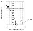
図6に入射光学系の像面湾曲を説明するための模式図を示す。図6(a)のΔmcolが入射光学系の像面湾曲、すなわち発光点間のピント差(入射光学系の光源位置差に換算されたピント差)を示す。また図6(b)は、発光点間のピント差が生じた場合の被走査面上のスポット径差を示す図であり、横軸がドラム位置を示すデフォーカス量を、縦軸がスポットの光軸からの位置を示す。図6(b)においてドラム位置(横軸=0)において、LD1のスポット径α1とLD16のスポット径α16が5μm異なっていることを示している。 FIG. 6 is a schematic diagram for explaining the curvature of field of the incident optical system. Δmcol in FIG. 6A represents the curvature of field of the incident optical system, that is, the focus difference between the light emitting points (focus difference converted to the light source position difference of the incident optical system). FIG. 6B is a diagram showing the spot diameter difference on the surface to be scanned when a focus difference occurs between the light emitting points. The horizontal axis indicates the defocus amount indicating the drum position, and the vertical axis indicates the spot. The position from the optical axis is shown. FIG. 6B shows that the spot diameter α1 of LD1 and the spot diameter α16 of LD16 are different by 5 μm at the drum position (horizontal axis = 0).
本実施例の光走査装置では、全点光源の像面湾曲のバランスを考慮して、点光源LD1とLD16の間の位置において入射光学系の像面湾曲がゼロとなるように、光源手段は配置されている。従って、軸上もしくはその近傍の発光点LD16(図4のLD16と同様)と主走査方向の最軸外発光点LD1(図4のLD1と同様)では、像面湾曲量の符号が異なる。つまり発光点LD16とLD1からの光束はともに、被走査面上でピント方向(X軸方向、すなわち光軸方向)にずれた位置に結像する。 In the optical scanning device of the present embodiment, the light source means is arranged so that the curvature of field of the incident optical system becomes zero at the position between the point light sources LD1 and LD16 in consideration of the balance of curvature of field of all point light sources. Has been placed. Therefore, the sign of the field curvature differs between the light emitting point LD16 on or near the axis (similar to LD16 in FIG. 4) and the most off-axis light emitting point LD1 in the main scanning direction (similar to LD1 in FIG. 4). That is, both the light beams from the light emitting points LD16 and LD1 are imaged at positions shifted in the focus direction (X-axis direction, that is, the optical axis direction) on the surface to be scanned.
本実施例において主走査方向における発光点LD16とLD1の被走査面7上での結像位置差(ピント差)ΔMは、|Δmcol|を同一波長に対する発光点LD16(光軸に最も近い軸上発光部)とLD1(光軸から最も離れた軸外発光部)の像面湾曲差、ffθを結像光学系の主走査断面内での焦点距離、fcolを入射光学系の主走査断面内での焦点距離、としたとき、
ΔM=|Δmcol|×(ffθ/fcol)2 (4)
で算出できる。本実施例におけるピント差ΔMは、
ΔM=0.0015×(250/75)2=0.017mm
である。通常、主走査方向のピント差ΔMは0.5mm以下であれば問題ない。すなわち、
ΔM=|Δmcol|×(ffθ/fcol)2≦0.5mm (5)
を満たしていると問題はない。さらに、小スポット高解像度対応光学系では光学素子の製造誤差や取り付け誤差を考慮すると、望ましくは、
ΔM=|Δmcol|×(ffθ/fcol)2≦0.2mm (5a)
さらに望ましくは、
ΔM=|Δmcol|×(ffθ/fcol)2≦0.05mm (5b)
を満たすようにすると良い。本実施例では、
|Δmcol|=0.0015
(ffθ/fcol)2=11.1
なので、
|Δmcol|×(ffθ/fcol)2=0.0167
であり、条件(5)、(5a)、(5b)を満足し、発光点間のスポット径のばらつきが小さい高解像の結像光学系を実現している。
In this embodiment, the imaging position difference (focus difference) ΔM between the light emitting points LD16 and LD1 in the main scanning direction on the surface to be scanned ΔM is equal to the light emitting point LD1 6 ( axis closest to the optical axis ) for the same wavelength. curvature difference of the upper light-emitting section) and the LD 1 (axis light emitting portion farthest from the optical axis), the focal length of the f f [theta] in the main scanning section of the imaging optical system, mainly the f col of the input optical system When the focal length is within the scanning section,
ΔM = | Δmcol | × (f fθ / f col ) 2 (4)
It can be calculated by The focus difference ΔM in this embodiment is
ΔM = 0.015 × (250/75) 2 = 0.017 mm
It is. Usually, there is no problem if the focus difference ΔM in the main scanning direction is 0.5 mm or less. That is,
ΔM = | Δmcol | × (f fθ / f col ) 2 ≦ 0.5 mm (5)
If it meets, there is no problem. Furthermore, in consideration of manufacturing errors and mounting errors of optical elements in a small spot high resolution compatible optical system,
ΔM = | Δmcol | × (f fθ / f col ) 2 ≦ 0.2 mm (5a)
More preferably,
ΔM = | Δmcol | × (f fθ / f col ) 2 ≦ 0.05 mm (5b)
It is better to satisfy. In this example,
| Δmcol | = 0.015
(F fθ / f col ) 2 = 11.1
So,
| Δmcol | × (f fθ / f col ) 2 = 0.0167
Thus, a high-resolution imaging optical system that satisfies the conditions (5), (5a), and (5b) and has a small variation in spot diameter between light emitting points is realized.
本実施例の入射光学系LAの主走査方向像面湾曲を図7に示す。図7において、横軸は光源位置換算のピントずれ量(単位:mm)を示し、縦軸は発光点位置(単位:mm)を示す。また、図8に、入射光学系が条件式(2)を満たさない場合の像面湾曲を比較例として示す。図7からもわかるように本実施例の入射光学系で発生する像面湾曲は、比較例として図8に示す条件式を満足しない入射光学系で構成した光学系の像面湾曲に比べ1/6以下に低減できる。 FIG. 7 shows the curvature of field in the main scanning direction of the incident optical system LA of the present embodiment. In FIG. 7, the horizontal axis indicates the amount of focus shift (unit: mm) in terms of the light source position, and the vertical axis indicates the light emitting point position (unit: mm). FIG. 8 shows, as a comparative example, curvature of field when the incident optical system does not satisfy the conditional expression (2). As can be seen from FIG. 7, the curvature of field generated in the incident optical system of the present embodiment is 1 / compared to the curvature of field of the optical system configured by the incident optical system that does not satisfy the conditional expression shown in FIG. It can be reduced to 6 or less.
(色収差低減について)
また、本実施例では、凸レンズと凹レンズを用いることで色収差も補正している。入射光学系に軸上色収差がある場合、レーザ光源の波長のばらつきにより被走査面でスポット径(ピント)がばらつくという問題が生じる。本実施例では、第1コリメータレンズ群を凸レンズと凹レンズの張り合わせレンズとし、凹レンズの分散が他の凸レンズの分散より大きくなる(アッベ数が小さくなる)ように構成している。具体的には、凹レンズのガラス材料としてアッベ数=25.68のs−tih11(OHARA社製)を用いている。
(About chromatic aberration reduction)
In this embodiment, chromatic aberration is also corrected by using a convex lens and a concave lens. When the incident optical system has axial chromatic aberration, there arises a problem that the spot diameter (focus) varies on the surface to be scanned due to variations in the wavelength of the laser light source. In this embodiment, the first collimator lens group is a cemented lens of a convex lens and a concave lens, and is configured such that the dispersion of the concave lens is larger (the Abbe number is smaller) than the dispersion of the other convex lenses. Specifically, s-tih11 (manufactured by OHARA) having an Abbe number of 25.68 is used as the glass material of the concave lens.
本実施例では、複数の光源間でレーザの発振波長が1.5nm異なった場合の入射光学系の軸上色収差による主走査方向および副走査方向のピント変化ΔT(1.5)が0.0005mmであり、
Δmcol>ΔT(1.5) (6)
を満たすように構成している。これにより、凹レンズを用いない場合に比べ、ピント差が無視できるレベルまで軸上色収差が補正されている。
In the present embodiment, the focus change ΔT (1.5) in the main scanning direction and the sub-scanning direction due to the longitudinal chromatic aberration of the incident optical system when the laser oscillation wavelength differs by 1.5 nm between the plurality of light sources is 0.0005 mm. And
Δmcol> ΔT (1.5) (6)
It is configured to satisfy. As a result, the axial chromatic aberration is corrected to a level at which the focus difference can be ignored compared to the case where no concave lens is used.
(入射光学系の調整方法について)
本発明の入射光学系は、光源と第1コリメータレンズ群の張り合わせレンズが同一部材に保持されており、製造工程において光源と第1コリメータレンズ群のレンズ間距離が調整されている。調整後、第1コリメータレンズ群は接着固定されて光源との間隔は固定される。その状態で光源と第1コリメータレンズ群を一体に保持した光源ユニットが走査装置本体に取り付けられる。また、走査装置本体においては、第2コリメータレンズ群の凸レンズを光軸方向に移動させることにより、主走査方向のピント位置を調整している。本実施例では、光軸方向位置ずれによるピント変化が大きい第1コリメータレンズ群と光源を一体の光源ユニットとすることで、より高精度な位置調整を可能としている。また、第2コリメータレンズ群を光走査装置内で独立に移動可能な構成とすることができるので、光源部以外の製造ばらつきで発生するピントずれも補正できる。すなわち、第1コリメーラレンズ群と第2コリメータレン群はそれぞれ独立に光軸方向の位置が調整可能に保持されている。また、入射光学系のレンズの中で主走査方向のパワーが最も弱いレンズである第2コリメータレンズは、光走査装置内で光軸方向に移動可能に保持されている。したがって、光源から第2コリメータレンズ群まで全てを一体的に保持した状態で操作装置本体に設置する場合に比べ、被走査面上のピント位置を高精度に調整できるというメリットを有する。尚、本実施例の副走査方向のピント位置は、副走査方向にのみパワーを有するシリンドリカルレンズ5を光軸方向に動かすことによって調整している。
(About the adjustment method of the incident optical system)
In the incident optical system of the present invention, the bonded lens of the light source and the first collimator lens group is held by the same member, and the distance between the light source and the first collimator lens group is adjusted in the manufacturing process. After the adjustment, the first collimator lens group is bonded and fixed, and the distance from the light source is fixed. In this state, a light source unit that integrally holds the light source and the first collimator lens group is attached to the scanning apparatus main body. In the scanning device main body, the focus position in the main scanning direction is adjusted by moving the convex lens of the second collimator lens group in the optical axis direction. In the present embodiment, the first collimator lens group and the light source, which have a large focus change due to the positional deviation in the optical axis direction, are integrated into a light source unit, thereby enabling more accurate position adjustment. In addition, since the second collimator lens group can be configured to be independently movable within the optical scanning device, it is possible to correct a focus shift caused by manufacturing variations other than the light source unit. That is, the first collimator lens group and the second collimator lens group are held independently so that their positions in the optical axis direction can be adjusted independently. The second collimator lens, which is the lens having the weakest power in the main scanning direction among the lenses of the incident optical system, is held so as to be movable in the optical axis direction in the optical scanning device. Therefore, there is an advantage that the focus position on the surface to be scanned can be adjusted with high accuracy compared to the case where the light source and the second collimator lens group are all held integrally in the operating device main body. In this embodiment, the focus position in the sub-scanning direction is adjusted by moving the
以上のように、本実施例の入射光学系のようにコリメータ光学系を2群で構成し、第2コリメータレンズ群(球面レンズ)のパワー配置と絞り位置を光軸方向に移動させて最適化することにより、マルチビーム間のピント差(スポット径差)を低減でき、高精細かつ高速な光走査装置を提供できる。 As described above, the collimator optical system is composed of two groups like the incident optical system of the present embodiment, and the power arrangement and the aperture position of the second collimator lens group (spherical lens) are moved in the optical axis direction for optimization. By doing so, the focus difference (spot diameter difference) between multiple beams can be reduced, and a high-definition and high-speed optical scanning device can be provided.
上記した本実施例においては、光源手段の複数の発光部の配置間隔の内、主走査方向と副走査方向とで広い方である主走査方向の光束幅を限定する絞りを第2コリメータレンズ群と光偏向器との間に設置し、式(2)を満たすよう構成することで本発明の効果を得た。しかし、本発明は例示した実施例1の構成に限定されることはない。すなわち、光源手段の複数の発光部の配置間隔の内、主走査方向と副走査方向とで広い方向の光束幅を限定する絞りを第2コリメータレンズ群と光偏向器との間に設置し、第2コリメータレンズ群の偏向器側のレンズ面から該絞りまでの距離L、入射光学系の、主走査方向及び副走査方向のうち前記発光部の配置間隔が広い方向における焦点距離fが、
0.5<|L|/f<2
を満足するよう構成することにより本発明の効果を得ることができる。
In the present embodiment described above, the second collimator lens group has a diaphragm for limiting the beam width in the main scanning direction, which is the wider in the main scanning direction and the sub-scanning direction, among the arrangement intervals of the plurality of light emitting units of the light source means. The effect of the present invention was obtained by installing between the optical deflector and the optical deflector so as to satisfy the formula (2). However, the present invention is not limited to the configuration of the illustrated first embodiment. That is, a diaphragm that limits the light beam width in a wide direction in the main scanning direction and the sub-scanning direction among the arrangement intervals of the plurality of light emitting units of the light source means is installed between the second collimator lens group and the optical deflector, The distance L from the lens surface on the deflector side of the second collimator lens group to the stop, the focal length f of the incident optical system in the direction in which the arrangement interval of the light emitting units is wide among the main scanning direction and the sub-scanning direction,
0.5 <| L | / f <2
The effect of the present invention can be obtained by configuring so as to satisfy the above.
本実施例の光走査装置において実施例1と異なる点は、光源レーザの発光点間隔と、入射光学系の構成である。結像光学系などのその他の構成は実施例1の光走査装置と同様である。 In the optical scanning apparatus of the present embodiment, the differences from the first embodiment are the light emitting point interval of the light source laser and the configuration of the incident optical system. Other configurations such as the imaging optical system are the same as those of the optical scanning apparatus of the first embodiment.
本実施例の入射光学系の概略の構成は図3に示した実施例1の構成と同様である。本実施例の光源は、図4に示した実施例1の光源と同様の光源であるが、実施例1では点光源のピッチが50μmであったのに対し、本実施例では25μmであることが異なる。このため、実施例1より同一ウエハーから多数のレーザを作成できるので、光源の製造コストを削減できるというメリットを有する。また、発光点間隔が実施例1より狭いため点光源の光軸からの離隔範囲が狭いので、光学系の像面湾曲の影響を受け難い構成としている。また、本実施例の入射光学系は第2の絞り6から第2コリメータレンズ群4の偏向器10側のレンズ面までの距離を40mmとし、実施例1に対して入射光学系の光路長を更に短縮し、更なる小型化が可能となる。
The schematic configuration of the incident optical system of the present embodiment is the same as that of the first embodiment shown in FIG. The light source of this example is the same as the light source of Example 1 shown in FIG. 4, but the pitch of the point light source is 50 μm in Example 1, whereas it is 25 μm in this example. Is different. For this reason, since many lasers can be produced from the same wafer from Example 1, it has the merit that the manufacturing cost of a light source can be reduced. In addition, since the distance between the light emitting points is narrower than that of the first embodiment, the distance range from the optical axis of the point light source is narrow, so that it is difficult to be affected by the curvature of field of the optical system. In the incident optical system of this embodiment, the distance from the
図9に近軸像面湾曲を示す。同図において、第2コリメータレンズ群4の偏向器10側のレンズ面から第2の絞り6までの距離Lの絶対値と像面湾曲量を示す収差係数を縦軸に示す。同図からL=40mmの近傍で近軸像面湾曲量がゼロになる点があり、その前後では線形に像面湾曲係数が増減している。本実施例ではL=36mmとしている。本実施例では、
|Δmcol|=0.00015(mm)
(ffθ/fcol)2=11.1
なので、
|Δmcol|×(ffθ/fcol)2=0.0167
であるので、条件(5)、(5a)、(5b)を満足し、良好に高解像の結像光学系を実現できる。
FIG. 9 shows paraxial field curvature. In the figure, the vertical axis indicates the absolute value of the distance L from the lens surface on the
| Δmcol | = 0.00015 (mm)
(F fθ / f col ) 2 = 11.1
So,
| Δmcol | × (f fθ / f col ) 2 = 0.0167
Therefore, conditions (5), (5a), and (5b) are satisfied, and a high resolution imaging optical system can be realized satisfactorily.
本実施例の入射光学系LAの主走査方向像面湾曲を図10に示す。図10において、横軸は光源位置換算のピントずれ量(単位:mm)を示し、縦軸は発光点位置(単位:mm)を示す。本実施例の入射光学系は、像面湾曲によるスポット径の差が発生し難い構成あり、高解像の結像光学系を実現している。 FIG. 10 shows the curvature of field in the main scanning direction of the incident optical system LA of the present embodiment. In FIG. 10, the horizontal axis indicates the amount of focus shift (unit: mm) in terms of light source position, and the vertical axis indicates the light emitting point position (unit: mm). The incident optical system of the present embodiment has a configuration in which a difference in spot diameter due to field curvature is unlikely to occur, and realizes a high-resolution imaging optical system.
また、本実施例においても、複数の光源間でレーザの発信波長が1.5nm異なった場合の入射光学系の軸上色収差による主走査方向および副走査方向のピント変化が0.0005mmであり、
ΔM>ΔT(1.5) (6)
を満たすように構成している。したがって、像面湾曲によるピント差と波長差によるピント変化の和は、
0.15μm+0.5μm=0.65μm
であり、被走査面でも7.2μmなので、スポット径の差は問題とならない。
Also in this embodiment, the focus change in the main scanning direction and the sub-scanning direction due to the axial chromatic aberration of the incident optical system when the transmission wavelength of the laser differs between the plurality of light sources by 1.5 nm is 0.0005 mm,
ΔM> ΔT (1.5) (6)
It is configured to satisfy. Therefore, the sum of the focus difference due to field curvature and the focus change due to wavelength difference is
0.15 μm + 0.5 μm = 0.65 μm
Since the surface to be scanned is 7.2 μm, the difference in spot diameter does not cause a problem.
表5に本実施例の入射光学系の数値データを示す。結像光学系等の数値データは実施例1と同様であるので省略する。 Table 5 shows numerical data of the incident optical system of this example. Since the numerical data of the imaging optical system and the like are the same as those in the first embodiment, a description thereof will be omitted.
表5:実施例2の入射光学系の数値データ
第1コリメータレンズ群と第2コリメータレンズ群の合成の主走査断面内での焦点距離(入射光学系の主走査断面内での焦点距離)は、レーザ光の取り込み量などで決定されており、本実施例では実施例1と同様に、=75mmとしている。また第2コリメータレンズ群の焦点距離は、335.1mmで第1コリメータレンズ群の焦点距離は88.5mmなのでパワー比は1/88.5:1/335.1≒4:1になるように構成されている。これは、第2コリメータレンズ群を本体内で光軸方向に移動させることにより、製造誤差で発生する主走査方向のピント位置を調整するためである。また、第1コリメータレンズ群を張り合わせレンズで構成することにより、調整、固定時の保持を容易に行えるようにしている。具体的には、
0.5 < 87/75 < 2
とし、式(1)を満足している。
The focal length in the main scanning section of the synthesis of the first collimator lens group and the second collimator lens group (focal length in the main scanning section of the incident optical system) is determined by the amount of laser light taken in, etc. In the present embodiment, as in the first embodiment, it is set to = 75 mm. Further, since the focal length of the second collimator lens group is 335.1 mm and the focal length of the first collimator lens group is 88.5 mm, the power ratio is 1 / 88.5: 1 / 335.1≈4: 1. It is configured. This is to adjust the focus position in the main scanning direction caused by a manufacturing error by moving the second collimator lens group in the optical axis direction within the main body. In addition, the first collimator lens group is formed of a bonded lens, so that it can be easily held during adjustment and fixing. In particular,
0.5 <87/75 <2
And the expression (1) is satisfied.
以上のように、本実施例の入射光学系のように2群の球面レンズのパワー配置と絞り位置を最適化することにより、マルチビーム間のピント差(スポット径差)を低減でき、よりコンパクトで高精彩かつ光束な光走査装置を提供できる。 As described above, by optimizing the power arrangement and aperture position of the two groups of spherical lenses as in the incident optical system of the present embodiment, the focus difference (spot diameter difference) between multiple beams can be reduced and more compact. Therefore, it is possible to provide a high-definition and luminous flux optical scanning device.
[画像形成装置]
図11は、本発明の第1又は第2の実施例で示した光走査装置を含む画像形成装置の実施例を示す副走査方向の要部断面図である。画像形成装置104には、パーソナルコンピュータの外部機器117からコードデータDcが入力される。コードデータDcは、画像形成装置内のプリンタコントローラ111によって、画像データ(ドットデータ)Diに変換される。画像データDiは、実施例1または2に示した構成を有する光走査ユニット100に入力される。光走査ユニット100からは、画像データDiに応じて変調された光ビーム103が出射され、この光ビーム103によって感光ドラム101の感光面が主走査方向に走査される。
[Image forming apparatus]
FIG. 11 is a cross-sectional view of a main part in the sub-scanning direction showing an embodiment of an image forming apparatus including the optical scanning device shown in the first or second embodiment of the present invention. Code data Dc is input to the
静電潜像担持体(感光体)たる感光ドラム101は、モータ115によって時計廻りに回転させられる。そして、この回転に伴って、感光ドラム101の感光面が光ビーム103に対して、主走査方向と直交する副走査方向に移動する。感光ドラム101の上方には、感光ドラム101の表面を一様に帯電せしめる帯電ローラ102が表面に当接するように設けられている。そして、帯電ローラ102によって帯電された感光ドラム101の表面に、前記光走査ユニット100によって走査される光ビーム103が照射されるようになっている。
The
先に説明したように、光ビーム103は、画像データDiに基づいて変調されており、この光ビーム103を照射することによって感光ドラム101の表面(感光体上)に静電潜像を形成せしめる。この静電潜像は、上記光ビーム103の照射位置よりもさらに感光ドラム101の回転方向の下流側で感光ドラム101に当接するように配設された現像器107によってトナー像として現像される。
As described above, the
現像器107によって現像されたトナー像は、感光ドラム101の下方で、感光ドラム101に対向するように配設された転写ローラ108によって被転写材たる用紙112上に転写される。用紙112は感光ドラム101の前方(図8において右側)の用紙カセット109内に収納されているが、手差しでも給紙が可能である。用紙カセット109端部には、給紙ローラ110が配設されており、用紙カセット109内の用紙112を搬送路へ送り込む。
The toner image developed by the developing
以上のようにして、未定着トナー像を転写された用紙112はさらに感光ドラム101後方(図11において左側)の定着器へと搬送される。定着器は内部に定着ヒータ(図示せず)を有する定着ローラ113とこの定着ローラ113に圧接するように配設された加圧ローラ114とで構成されている。そして転写部から搬送されてきた用紙112を定着ローラ113と加圧ローラ114の圧接部にて加圧しながら加熱することにより用紙112上の未定着トナー像を定着せしめる。更に定着ローラ113の後方には排紙ローラ116が配設されており、定着された用紙112を画像形成装置の外に排出せしめる。
As described above, the
図8においては図示していないが、プリントコントローラ111は、先に説明したデータの変換だけでなく、モータ115を始め画像形成装置内の各部や、後述する光走査ユニット内の駆動モータなどの制御を行う。
Although not shown in FIG. 8, the
本発明で使用される画像形成装置の記録密度は、限定されない。しかし、記録密度が高くなればなるほど、高い画質が求められることを考えると、1200dpi以上の画像形成装置において本発明の実施例1または2の構成はより効果を発揮する。 The recording density of the image forming apparatus used in the present invention is not limited. However, considering that the higher the recording density, the higher the image quality is required, the configuration of the first or second embodiment of the present invention is more effective in an image forming apparatus of 1200 dpi or more.
[カラー画像形成装置]
図12は本発明の第1又は第2の実施例で示した光走査装置を含むカラー画像形成装置の実施例の要部概略図である。本実施例は、光走査装置(光結像光学系)を4個並べ各々並行して像担持体である感光ドラム面上に画像情報を記録するタンデムタイプのカラー画像形成装置である。図12において、60はカラー画像形成装置、11,12,13,14は各々実施例1または2に示した構成を有する光走査装置、21,22,23,24は各々像担持体としての感光ドラム、31,32,33,34は各々現像器、51は搬送ベルトである。尚、図12においては現像器で現像されたトナー像を被転写材に転写する転写器(不図示)と、転写されたトナー像を被転写材に定着させる定着器(不図示)とを有している。
[Color image forming apparatus]
FIG. 12 is a schematic view of the essential portions of an embodiment of a color image forming apparatus including the optical scanning device shown in the first or second embodiment of the present invention. This embodiment is a tandem type color image forming apparatus in which four optical scanning devices (optical imaging optical systems) are arranged in parallel and image information is recorded on a photosensitive drum surface as an image carrier. In FIG. 12, 60 is a color image forming apparatus, 11, 12, 13, and 14 are optical scanning devices each having the configuration shown in the first or second embodiment, and 21, 22, 23, and 24 are photosensitive members as image carriers.
図12において、カラー画像形成装置60には、パーソナルコンピュータの外部機器52からR(レッド)、G(グリーン)、B(ブルー)の各色信号が入力する。これらの色信号は、装置内のプリンタコントローラ53によって、C(シアン),M(マゼンタ),Y(イエロー)、B(ブラック)の各画像データ(ドットデータ)に変換される。これらの画像データは、それぞれ光走査装置11,12,13,14に入力される。そして、これらの光走査装置からは、各画像データに応じて変調された光ビーム41,42,43,44が射出され、これらの光ビームによって感光ドラム21,22,23,24の感光面が主走査方向に走査される。
In FIG. 12, the color
本実施例におけるカラー画像形成装置は光走査装置(11,12,13,14)を4個並べ、各々がC(シアン),M(マゼンタ),Y(イエロー)、B(ブラック)の各色に対応している。そして各々平行して感光ドラム21,22,23,24面上に画像信号(画像情報)を記録し、カラー画像を高速に印字するものである。
The color image forming apparatus in this embodiment has four optical scanning devices (11, 12, 13, and 14) arranged in each color of C (cyan), M (magenta), Y (yellow), and B (black). It corresponds. In parallel, image signals (image information) are recorded on the surfaces of the
本実施例におけるカラー画像形成装置は上述の如く4つの光走査装置11,12,13,14により各々の画像データに基づいた光ビームを用いて各色の潜像を各々対応する感光ドラム21,22,23,24面上に形成している。その後、記録材に多重転写して1枚のフルカラー画像を形成している。
As described above, the color image forming apparatus in this embodiment uses the light beams based on the respective image data by the four
前記外部機器52としては、CCDセンサを備えたカラー画像読取装置が用いられても良い。この場合には、このカラー画像読取装置と、カラー画像形成装置60とで、カラーデジタル複写機が構成される。
As the external device 52, a color image reading device including a CCD sensor may be used. In this case, the color image reading apparatus and the color
1 光源手段(面発光レーザ)
3 コリメータレンズ
4 シリンドリカルレンズ
5 第2の絞り
10 偏向手段(ポリゴンミラー)
10a 偏向面
20 結像光学系(走査光学系)
20a 第1の結像レンズ
20b 第2の結像レンズ
11、12、13、14 光走査装置
100 光走査装置
1 Light source means (surface emitting laser)
3
20a
Claims (12)
前記入射光学系は、前記光源からの光束の収束度を変換する第1光学系と、主走査方向及び副走査方向のうち前記発光部の配置間隔が広い方である第1方向において前記第1光学系からの光束の幅を制限する絞りと、を有し、
前記第1光学系は、非球面を含まない光学素子で構成される、前記光源の側から順に配置された第1光学素子群と第2光学素子群とを有し、
前記第2光学素子群の前記偏向器に最も近い光学面から前記絞りまでの距離をL、前記第1方向と光軸方向とに平行な第1断面内における前記入射光学系の焦点距離をf、とするとき、
0.5<|L|/f<2
なる条件を満足することを特徴とする光走査装置。 A light source having a plurality of light emitting units, a deflector that deflects a light beam from the light source and scans a surface to be scanned in a main scanning direction, and an incident optical system that causes light from the light source to enter the deflector. An optical scanning device comprising:
The incident optical system includes: a first optical system that converts a convergence degree of a light beam from the light source; and a first direction in which a light emitting unit is disposed at a wider interval between a main scanning direction and a sub scanning direction. A diaphragm for limiting the width of the light beam from the optical system,
The first optical system includes a first optical element group and a second optical element group arranged in order from the light source side, which are configured by optical elements not including an aspherical surface,
The distance from the optical surface closest to the deflector of the second optical element group to the stop is L, and the focal length of the incident optical system in the first cross section parallel to the first direction and the optical axis direction is f. , And when
0.5 <| L | / f <2
An optical scanning device characterized by satisfying the following conditions.
0.1<fcol1/fcol2<1/3
なる条件を満足することを特徴とする請求項1又は2に記載の光走査装置。 In the first cross section, the first optical element group has a positive power, the second optical element group has a weaker positive power than the first optical element group, and the first optical element group Is set to f col1, and the focal length of the second optical element group is f col2 .
0.1 <f col1 / f col2 <1/3
The optical scanning device according to claim 1, wherein the following condition is satisfied.
|Δmcol|×(ffθ/fcol)2≦0.5mm
なる条件を満たすことを特徴とする請求項1乃至5のいずれか1項に記載の光走査装置。 An imaging optical system that guides a light beam from the deflector to the surface to be scanned is provided. In the first cross section, the focal length of the imaging optical system is f fθ and the focal length of the incident optical system is f col. When the first light beam from the on-axis light emitting unit and the second light beam from the most off- axis light emitting unit in the light source have the same wavelength, the incident optical system has the first light beam and the second light beam. When the focus difference is Δmcol,
| Δmcol | × (f fθ / f col ) 2 ≦ 0.5 mm
The optical scanning device according to claim 1, wherein the following condition is satisfied.
0.1<fcol1/fcol2<1/3
なる条件を満足することを特徴とする請求項7に記載の光走査装置。 In the first cross section, when the focal length of the first optical element group is f col1 and the focal length of the second optical element group is f col2 ,
0.1 <f col1 / f col2 <1/3
The optical scanning device according to claim 7, wherein the following condition is satisfied.
Priority Applications (1)
| Application Number | Priority Date | Filing Date | Title |
|---|---|---|---|
| JP2013139744A JP6234085B2 (en) | 2013-07-03 | 2013-07-03 | Optical scanning device and image forming apparatus using the same |
Applications Claiming Priority (1)
| Application Number | Priority Date | Filing Date | Title |
|---|---|---|---|
| JP2013139744A JP6234085B2 (en) | 2013-07-03 | 2013-07-03 | Optical scanning device and image forming apparatus using the same |
Publications (3)
| Publication Number | Publication Date |
|---|---|
| JP2015014639A JP2015014639A (en) | 2015-01-22 |
| JP2015014639A5 JP2015014639A5 (en) | 2016-07-28 |
| JP6234085B2 true JP6234085B2 (en) | 2017-11-22 |
Family
ID=52436408
Family Applications (1)
| Application Number | Title | Priority Date | Filing Date |
|---|---|---|---|
| JP2013139744A Active JP6234085B2 (en) | 2013-07-03 | 2013-07-03 | Optical scanning device and image forming apparatus using the same |
Country Status (1)
| Country | Link |
|---|---|
| JP (1) | JP6234085B2 (en) |
Family Cites Families (6)
| Publication number | Priority date | Publication date | Assignee | Title |
|---|---|---|---|---|
| JPH02181712A (en) * | 1989-01-09 | 1990-07-16 | Canon Inc | Achromatic optical system for laser scanning |
| JP2002006211A (en) * | 2000-06-23 | 2002-01-09 | Canon Inc | Temperature compensation lens and optical device using the same |
| JP2008052197A (en) * | 2006-08-28 | 2008-03-06 | Canon Inc | Optical scanner and image forming apparatus using the same |
| JP5041587B2 (en) * | 2007-05-09 | 2012-10-03 | 株式会社リコー | Optical scanning apparatus and image forming apparatus |
| JP5103673B2 (en) * | 2008-06-23 | 2012-12-19 | 株式会社リコー | Optical scanning device and image forming apparatus |
| WO2014103654A1 (en) * | 2012-12-27 | 2014-07-03 | 富士フイルム株式会社 | Light beam scanning device and radiation image reading device |
-
2013
- 2013-07-03 JP JP2013139744A patent/JP6234085B2/en active Active
Also Published As
| Publication number | Publication date |
|---|---|
| JP2015014639A (en) | 2015-01-22 |
Similar Documents
| Publication | Publication Date | Title |
|---|---|---|
| KR100485315B1 (en) | Scanning optical device and image forming apparatus using the same | |
| US7929007B2 (en) | Optical scanning device and image forming apparatus | |
| JP4684470B2 (en) | Optical scanning device and image forming apparatus using the same | |
| JP2004070107A (en) | Optical scanner and image forming apparatus using the same | |
| JP5896651B2 (en) | Optical scanning device and image forming apparatus using the same | |
| KR100856154B1 (en) | Optical scanning apparatus and image-forming apparatus using the same | |
| JP6351257B2 (en) | Optical scanning device and image forming apparatus having the same | |
| JP5173879B2 (en) | Optical scanning device and image forming apparatus using the same | |
| JP2015125210A5 (en) | ||
| JP2007114484A (en) | Optical scanner and image forming device using it | |
| JP2008052197A (en) | Optical scanner and image forming apparatus using the same | |
| JP5300505B2 (en) | Method for adjusting optical scanning device | |
| JP4455308B2 (en) | Optical scanning device and image forming apparatus using the same | |
| JP2005134624A (en) | Optical scanner and image forming apparatus using same | |
| JP5127122B2 (en) | Method for adjusting scanning line pitch interval of scanning optical device | |
| JP4455309B2 (en) | Optical scanning device and image forming apparatus using the same | |
| JP6234085B2 (en) | Optical scanning device and image forming apparatus using the same | |
| JP5094221B2 (en) | Optical scanning device and image forming apparatus using the same | |
| JP4240777B2 (en) | Scanning optical device and image forming apparatus using the same | |
| JP4401950B2 (en) | Optical scanning device and image forming apparatus using the same | |
| JP4378416B2 (en) | Scanning optical device and image forming apparatus using the same | |
| JP7373365B2 (en) | optical scanning device | |
| JP4401951B2 (en) | Optical scanning device and image forming apparatus using the same | |
| JP2018151423A (en) | Optical scanner and image forming apparatus including the same | |
| JP4612839B2 (en) | Method for adjusting color image forming apparatus |
Legal Events
| Date | Code | Title | Description |
|---|---|---|---|
| A521 | Written amendment |
Free format text: JAPANESE INTERMEDIATE CODE: A523 Effective date: 20160609 |
|
| A621 | Written request for application examination |
Free format text: JAPANESE INTERMEDIATE CODE: A621 Effective date: 20160609 |
|
| A977 | Report on retrieval |
Free format text: JAPANESE INTERMEDIATE CODE: A971007 Effective date: 20170215 |
|
| A131 | Notification of reasons for refusal |
Free format text: JAPANESE INTERMEDIATE CODE: A131 Effective date: 20170221 |
|
| A521 | Written amendment |
Free format text: JAPANESE INTERMEDIATE CODE: A523 Effective date: 20170413 |
|
| TRDD | Decision of grant or rejection written | ||
| A01 | Written decision to grant a patent or to grant a registration (utility model) |
Free format text: JAPANESE INTERMEDIATE CODE: A01 Effective date: 20170926 |
|
| A61 | First payment of annual fees (during grant procedure) |
Free format text: JAPANESE INTERMEDIATE CODE: A61 Effective date: 20171024 |
|
| R151 | Written notification of patent or utility model registration |
Ref document number: 6234085 Country of ref document: JP Free format text: JAPANESE INTERMEDIATE CODE: R151 |