JP6149977B1 - Voltage converter and leakage inductance determination method - Google Patents
Voltage converter and leakage inductance determination method Download PDFInfo
- Publication number
- JP6149977B1 JP6149977B1 JP2016116530A JP2016116530A JP6149977B1 JP 6149977 B1 JP6149977 B1 JP 6149977B1 JP 2016116530 A JP2016116530 A JP 2016116530A JP 2016116530 A JP2016116530 A JP 2016116530A JP 6149977 B1 JP6149977 B1 JP 6149977B1
- Authority
- JP
- Japan
- Prior art keywords
- inductors
- inductor
- leakage inductance
- ripple current
- voltage conversion
- Prior art date
- Legal status (The legal status is an assumption and is not a legal conclusion. Google has not performed a legal analysis and makes no representation as to the accuracy of the status listed.)
- Active
Links
Images


Classifications
-
- H—ELECTRICITY
- H01—ELECTRIC ELEMENTS
- H01F—MAGNETS; INDUCTANCES; TRANSFORMERS; SELECTION OF MATERIALS FOR THEIR MAGNETIC PROPERTIES
- H01F27/00—Details of transformers or inductances, in general
- H01F27/28—Coils; Windings; Conductive connections
-
- H—ELECTRICITY
- H02—GENERATION; CONVERSION OR DISTRIBUTION OF ELECTRIC POWER
- H02M—APPARATUS FOR CONVERSION BETWEEN AC AND AC, BETWEEN AC AND DC, OR BETWEEN DC AND DC, AND FOR USE WITH MAINS OR SIMILAR POWER SUPPLY SYSTEMS; CONVERSION OF DC OR AC INPUT POWER INTO SURGE OUTPUT POWER; CONTROL OR REGULATION THEREOF
- H02M1/00—Details of apparatus for conversion
- H02M1/08—Circuits specially adapted for the generation of control voltages for semiconductor devices incorporated in static converters
-
- H—ELECTRICITY
- H02—GENERATION; CONVERSION OR DISTRIBUTION OF ELECTRIC POWER
- H02M—APPARATUS FOR CONVERSION BETWEEN AC AND AC, BETWEEN AC AND DC, OR BETWEEN DC AND DC, AND FOR USE WITH MAINS OR SIMILAR POWER SUPPLY SYSTEMS; CONVERSION OF DC OR AC INPUT POWER INTO SURGE OUTPUT POWER; CONTROL OR REGULATION THEREOF
- H02M1/00—Details of apparatus for conversion
- H02M1/14—Arrangements for reducing ripples from DC input or output
-
- H—ELECTRICITY
- H02—GENERATION; CONVERSION OR DISTRIBUTION OF ELECTRIC POWER
- H02M—APPARATUS FOR CONVERSION BETWEEN AC AND AC, BETWEEN AC AND DC, OR BETWEEN DC AND DC, AND FOR USE WITH MAINS OR SIMILAR POWER SUPPLY SYSTEMS; CONVERSION OF DC OR AC INPUT POWER INTO SURGE OUTPUT POWER; CONTROL OR REGULATION THEREOF
- H02M3/00—Conversion of DC power input into DC power output
- H02M3/02—Conversion of DC power input into DC power output without intermediate conversion into AC
- H02M3/04—Conversion of DC power input into DC power output without intermediate conversion into AC by static converters
- H02M3/10—Conversion of DC power input into DC power output without intermediate conversion into AC by static converters using discharge tubes with control electrode or semiconductor devices with control electrode
- H02M3/145—Conversion of DC power input into DC power output without intermediate conversion into AC by static converters using discharge tubes with control electrode or semiconductor devices with control electrode using devices of a triode or transistor type requiring continuous application of a control signal
- H02M3/155—Conversion of DC power input into DC power output without intermediate conversion into AC by static converters using discharge tubes with control electrode or semiconductor devices with control electrode using devices of a triode or transistor type requiring continuous application of a control signal using semiconductor devices only
- H02M3/156—Conversion of DC power input into DC power output without intermediate conversion into AC by static converters using discharge tubes with control electrode or semiconductor devices with control electrode using devices of a triode or transistor type requiring continuous application of a control signal using semiconductor devices only with automatic control of output voltage or current, e.g. switching regulators
- H02M3/158—Conversion of DC power input into DC power output without intermediate conversion into AC by static converters using discharge tubes with control electrode or semiconductor devices with control electrode using devices of a triode or transistor type requiring continuous application of a control signal using semiconductor devices only with automatic control of output voltage or current, e.g. switching regulators including plural semiconductor devices as final control devices for a single load
- H02M3/1584—Conversion of DC power input into DC power output without intermediate conversion into AC by static converters using discharge tubes with control electrode or semiconductor devices with control electrode using devices of a triode or transistor type requiring continuous application of a control signal using semiconductor devices only with automatic control of output voltage or current, e.g. switching regulators including plural semiconductor devices as final control devices for a single load with a plurality of power processing stages connected in parallel
-
- H—ELECTRICITY
- H02—GENERATION; CONVERSION OR DISTRIBUTION OF ELECTRIC POWER
- H02M—APPARATUS FOR CONVERSION BETWEEN AC AND AC, BETWEEN AC AND DC, OR BETWEEN DC AND DC, AND FOR USE WITH MAINS OR SIMILAR POWER SUPPLY SYSTEMS; CONVERSION OF DC OR AC INPUT POWER INTO SURGE OUTPUT POWER; CONTROL OR REGULATION THEREOF
- H02M3/00—Conversion of DC power input into DC power output
- H02M3/02—Conversion of DC power input into DC power output without intermediate conversion into AC
- H02M3/04—Conversion of DC power input into DC power output without intermediate conversion into AC by static converters
- H02M3/10—Conversion of DC power input into DC power output without intermediate conversion into AC by static converters using discharge tubes with control electrode or semiconductor devices with control electrode
- H02M3/145—Conversion of DC power input into DC power output without intermediate conversion into AC by static converters using discharge tubes with control electrode or semiconductor devices with control electrode using devices of a triode or transistor type requiring continuous application of a control signal
- H02M3/155—Conversion of DC power input into DC power output without intermediate conversion into AC by static converters using discharge tubes with control electrode or semiconductor devices with control electrode using devices of a triode or transistor type requiring continuous application of a control signal using semiconductor devices only
- H02M3/156—Conversion of DC power input into DC power output without intermediate conversion into AC by static converters using discharge tubes with control electrode or semiconductor devices with control electrode using devices of a triode or transistor type requiring continuous application of a control signal using semiconductor devices only with automatic control of output voltage or current, e.g. switching regulators
- H02M3/158—Conversion of DC power input into DC power output without intermediate conversion into AC by static converters using discharge tubes with control electrode or semiconductor devices with control electrode using devices of a triode or transistor type requiring continuous application of a control signal using semiconductor devices only with automatic control of output voltage or current, e.g. switching regulators including plural semiconductor devices as final control devices for a single load
- H02M3/1588—Conversion of DC power input into DC power output without intermediate conversion into AC by static converters using discharge tubes with control electrode or semiconductor devices with control electrode using devices of a triode or transistor type requiring continuous application of a control signal using semiconductor devices only with automatic control of output voltage or current, e.g. switching regulators including plural semiconductor devices as final control devices for a single load comprising at least one synchronous rectifier element
-
- H—ELECTRICITY
- H02—GENERATION; CONVERSION OR DISTRIBUTION OF ELECTRIC POWER
- H02M—APPARATUS FOR CONVERSION BETWEEN AC AND AC, BETWEEN AC AND DC, OR BETWEEN DC AND DC, AND FOR USE WITH MAINS OR SIMILAR POWER SUPPLY SYSTEMS; CONVERSION OF DC OR AC INPUT POWER INTO SURGE OUTPUT POWER; CONTROL OR REGULATION THEREOF
- H02M3/00—Conversion of DC power input into DC power output
- H02M3/02—Conversion of DC power input into DC power output without intermediate conversion into AC
- H02M3/04—Conversion of DC power input into DC power output without intermediate conversion into AC by static converters
- H02M3/10—Conversion of DC power input into DC power output without intermediate conversion into AC by static converters using discharge tubes with control electrode or semiconductor devices with control electrode
- H02M3/145—Conversion of DC power input into DC power output without intermediate conversion into AC by static converters using discharge tubes with control electrode or semiconductor devices with control electrode using devices of a triode or transistor type requiring continuous application of a control signal
- H02M3/155—Conversion of DC power input into DC power output without intermediate conversion into AC by static converters using discharge tubes with control electrode or semiconductor devices with control electrode using devices of a triode or transistor type requiring continuous application of a control signal using semiconductor devices only
- H02M3/156—Conversion of DC power input into DC power output without intermediate conversion into AC by static converters using discharge tubes with control electrode or semiconductor devices with control electrode using devices of a triode or transistor type requiring continuous application of a control signal using semiconductor devices only with automatic control of output voltage or current, e.g. switching regulators
- H02M3/158—Conversion of DC power input into DC power output without intermediate conversion into AC by static converters using discharge tubes with control electrode or semiconductor devices with control electrode using devices of a triode or transistor type requiring continuous application of a control signal using semiconductor devices only with automatic control of output voltage or current, e.g. switching regulators including plural semiconductor devices as final control devices for a single load
- H02M3/1584—Conversion of DC power input into DC power output without intermediate conversion into AC by static converters using discharge tubes with control electrode or semiconductor devices with control electrode using devices of a triode or transistor type requiring continuous application of a control signal using semiconductor devices only with automatic control of output voltage or current, e.g. switching regulators including plural semiconductor devices as final control devices for a single load with a plurality of power processing stages connected in parallel
- H02M3/1586—Conversion of DC power input into DC power output without intermediate conversion into AC by static converters using discharge tubes with control electrode or semiconductor devices with control electrode using devices of a triode or transistor type requiring continuous application of a control signal using semiconductor devices only with automatic control of output voltage or current, e.g. switching regulators including plural semiconductor devices as final control devices for a single load with a plurality of power processing stages connected in parallel switched with a phase shift, i.e. interleaved
-
- Y—GENERAL TAGGING OF NEW TECHNOLOGICAL DEVELOPMENTS; GENERAL TAGGING OF CROSS-SECTIONAL TECHNOLOGIES SPANNING OVER SEVERAL SECTIONS OF THE IPC; TECHNICAL SUBJECTS COVERED BY FORMER USPC CROSS-REFERENCE ART COLLECTIONS [XRACs] AND DIGESTS
- Y02—TECHNOLOGIES OR APPLICATIONS FOR MITIGATION OR ADAPTATION AGAINST CLIMATE CHANGE
- Y02B—CLIMATE CHANGE MITIGATION TECHNOLOGIES RELATED TO BUILDINGS, e.g. HOUSING, HOUSE APPLIANCES OR RELATED END-USER APPLICATIONS
- Y02B70/00—Technologies for an efficient end-user side electric power management and consumption
- Y02B70/10—Technologies improving the efficiency by using switched-mode power supplies [SMPS], i.e. efficient power electronics conversion e.g. power factor correction or reduction of losses in power supplies or efficient standby modes
Landscapes
- Engineering & Computer Science (AREA)
- Power Engineering (AREA)
- Dc-Dc Converters (AREA)
Abstract
【課題】磁気相殺する2つのインダクタが巻回されたコアのサイズを低減した電圧変換装置、及び前記コアのサイズを低減することが可能な漏れインダクタンス決定方法を提供する。
【解決手段】制御部50aが電圧変換回路1aのFET11及び12を交互にオン/オフし、コア20に巻回されて互いに磁気を打ち消し合うインダクタ21及び22夫々に流れる電流をFET11及び12でスイッチングすることにより、電圧変換回路1aに入力された電圧が変換されて出力される。インダクタ21及び22は、漏れインダクタンスと密接に関係する結合係数kが−0.99≦k≦−0.78の範囲内にある。
【選択図】図1The present invention provides a voltage converter in which the size of a core around which two inductors for magnetic cancellation are wound is reduced, and a leakage inductance determination method capable of reducing the size of the core.
A control unit 50a alternately turns on and off FETs 11 and 12 of a voltage conversion circuit 1a and switches currents flowing in inductors 21 and 22 that are wound around a core 20 and cancel each other's magnetism, using the FETs 11 and 12. As a result, the voltage input to the voltage conversion circuit 1a is converted and output. Inductors 21 and 22 have a coupling coefficient k closely related to the leakage inductance in a range of −0.99 ≦ k ≦ −0.78.
[Selection] Figure 1
Description
本発明は、コアに巻回されて磁気相殺する2つのインダクタ夫々に流れる電流をスイッチング素子でスイッチングする電圧変換装置及び漏れインダクタンス決定方法に関する。 The present invention relates to a voltage converter and a leakage inductance determination method in which currents flowing through two inductors wound around a core and magnetically cancel each other are switched by a switching element.
直流電圧を昇圧又は降圧して所望の直流電圧に変換するDC/DCコンバータ(以下、単にコンバータという)が様々な分野で使用されている。コンバータは、インダクタに流れる電流をスイッチングすることによって所要の電圧を出力する。出力電流を大きくすると共に出力電流のリップルを小さくし、且つ装置の小型化を図るために、複数のコンバータを互いに異なる位相で作動させて並列に接続したマルチフェーズ(多相)コンバータが利用されている。 2. Description of the Related Art DC / DC converters (hereinafter simply referred to as converters) that increase or decrease DC voltage and convert it to a desired DC voltage are used in various fields. The converter outputs a required voltage by switching the current flowing through the inductor. In order to increase the output current, reduce the ripple of the output current, and reduce the size of the device, a multi-phase converter in which a plurality of converters are operated in different phases and connected in parallel is used. Yes.
例えば特許文献1には、同一のコア上に互いに逆方向に巻回された第1及び第2のコイルと一対のスイッチとを用いて第1及び第2夫々のコイルに交互に励磁電流を流すことにより、第2及び第1のコイルにコアの磁束を相殺する方向に電流を発生させ、第2及び第1のコイルからの電流をダイオードで足し合わせて出力する昇圧型のDC/DCコンバータが記載されている。このDC/DCコンバータは、第1及び第2のコイルによるコアの磁化が相殺されるため、コアの磁気飽和が抑制されてコアの小型化が可能になるものである。
For example, in
特許文献1に記載された技術を用いた所謂インターリーブ型のDC/DCコンバータでは、第1及び第2のコイル間の結合係数と、第1及び第2のコイル内のリップル電流とが密接に関連することが知られている。この点に着目して、特許文献2では、第1及び第2のコイルに相当する2つのインダクタに流れる電流を5%乃至40%の範囲のデューティ比でスイッチングする場合に、インダクタ間の結合係数kが−0.4<k≦−0.1の範囲内にあるようにすることにより、kが0のときよりもリップル電流を低減する技術が開示されている。
In a so-called interleaved DC / DC converter using the technique described in
しかしながら、特許文献1に開示された技術は、インダクタに流れる電流をスイッチングするデューティ比が50%を超えるとインダクタが短絡状態になるとの記載があることから、漏れインダクタンスが限りなく0に近いインダクタ、換言すればkが実質的に−1であるインダクタが想定されており、デューティ比の可変範囲に大きな制約がある。
However, the technique disclosed in
また、特許文献2に開示された技術は、自己インダクタンスが一定である2つのインダクタが一定サイズのコアに巻回されている(記載内容からそのように解される)場合に、結合係数kが0のときよりもインダクタのリップル電流が低減されるkの範囲を開示するものであって、コアのサイズを小さくすることを課題とするものではなかった。このため、特許文献2には、結合係数kが0のときと比較してインダクタのリップル電流が増加しない範囲でコアのサイズを小さくする技術は開示も示唆もされていない。
Further, in the technique disclosed in
本発明は、斯かる事情に鑑みてなされたものであり、その目的とするところは、磁気相殺する2つのインダクタが巻回されたコアのサイズを低減した電圧変換装置、及び前記コアのサイズを低減することが可能な漏れインダクタンス決定方法を提供することにある。 The present invention has been made in view of such circumstances, and an object of the present invention is to provide a voltage conversion device in which the size of a core around which two inductors for magnetic cancellation are wound is reduced, and the size of the core. An object of the present invention is to provide a leakage inductance determination method that can be reduced.
本発明の一態様に係る電圧変換装置は、コアに巻回されて磁気相殺する2つのインダクタ及び夫々のインダクタに流れる電流をスイッチングするスイッチング素子を有する電圧変換回路と、各スイッチング素子を交互にオン/オフする制御部とを備える電圧変換装置であって、前記2つのインダクタの漏れインダクタンスの大きさは、前記2つのインダクタの結合係数が0である場合に、前記2つのインダクタに流れるリップル電流を所定の低減率で低減するために必要とされる自己インダクタンスの大きさの1倍未満、且つ0.45倍以上の大きさであり、前記2つのインダクタの結合係数は、−0.99以上、且つ−0.78以下の範囲内にある。 A voltage conversion device according to an aspect of the present invention includes two inductors that are wound around a core and magnetically cancel each other, a voltage conversion circuit that includes a switching element that switches a current flowing through each inductor, and each switching element that is turned on alternately. A voltage conversion device including a control unit for turning off, wherein the magnitude of the leakage inductance of the two inductors is a ripple current flowing through the two inductors when a coupling coefficient of the two inductors is zero. The self-inductance required for reduction at a predetermined reduction rate is less than 1 time and 0.45 times or more, and the coupling coefficient of the two inductors is −0.99 or more, And it exists in the range of -0.78 or less.
本発明の一態様に係る漏れインダクタンスの決定方法は、コアに巻回されて磁気相殺する2つのインダクタ夫々に流れる電流を、制御部がオン/オフするスイッチング素子でスイッチングする電圧変換装置における前記2つのインダクタの漏れインダクタンスを決定する方法であって、結合係数が0である2つの第1インダクタと、該第1インダクタの自己インダクタンスと同じ大きさの漏れインダクタンスを有しており結合係数を−1に近づけた2つの第2インダクタとを用意し、前記2つのインダクタに代えて前記2つの第1インダクタを接続し、該第1インダクタに流れるリップル電流について、前記制御部が各スイッチング素子をオンする所定範囲のデューティ比に対する第1変化特性を取得し、前記2つの第1インダクタに代えて前記2つの第2インダクタを接続し、該第2インダクタに流れるリップル電流について、前記所定範囲のデューティ比に対する第2変化特性を取得し、取得した第1及び第2変化特性を比較した結果に基づいてリップル電流の低減率を算出し、前記第2インダクタの漏れインダクタンスの大きさの低減率を、前記算出したリップル電流の低減率以下の低減率とし、該低減率となるように前記2つのインダクタの漏れインダクタンスの大きさを決定し、前記2つの第2インダクタの結合係数を前記2つのインダクタの結合係数にする。 According to another aspect of the present invention, there is provided a method for determining a leakage inductance, wherein the current flowing in each of two inductors wound around a core and magnetically canceled is switched by a switching element that is turned on / off by a control unit. This is a method for determining the leakage inductance of two inductors, including two first inductors having a coupling coefficient of 0, a leakage inductance having the same magnitude as the self-inductance of the first inductor, and a coupling coefficient of −1. Two second inductors close to each other are prepared, the two first inductors are connected instead of the two inductors, and the control unit turns on each switching element for a ripple current flowing through the first inductor. Obtaining a first change characteristic for a duty ratio in a predetermined range, instead of the two first inductors Based on the result obtained by connecting the two second inductors, acquiring the second change characteristic with respect to the duty ratio in the predetermined range, and comparing the acquired first and second change characteristics for the ripple current flowing through the second inductor. The reduction rate of the ripple current is calculated, and the reduction rate of the leakage inductance of the second inductor is set to a reduction rate equal to or less than the calculated reduction rate of the ripple current, and the two inductors are set so as to be the reduction rate. determines the size of the data of the leakage inductance and the coupling coefficient of the two second inductor coupling coefficient of said two inductors.
なお、本願は、このような特徴的な処理部及びステップを夫々備える電圧変換装置及び漏れインダクタンスの決定方法として実現することができるだけでなく、電圧変換装置の一部又は全部を半導体集積回路として実現したり、電圧変換装置を含むその他のシステムとして実現したりすることができる。 The present application can be realized not only as a voltage conversion device and a leakage inductance determination method each having such characteristic processing units and steps, but also as a semiconductor integrated circuit in which part or all of the voltage conversion device is realized. Or other system including a voltage converter.
上記によれば、磁気相殺する2つのインダクタが巻回されたコアのサイズを低減することが可能となる。 According to the above, it is possible to reduce the size of the core around which the two inductors for magnetic cancellation are wound.
[本発明の実施形態の説明]
最初に本発明の実施態様を列記して説明する。また、以下に記載する実施形態の少なくとも一部を任意に組み合わせてもよい。
[Description of Embodiment of the Present Invention]
First, embodiments of the present invention will be listed and described. Moreover, you may combine arbitrarily at least one part of embodiment described below.
(1)本発明の一態様に係る電圧変換装置は、コアに巻回されて磁気相殺する2つのインダクタ及び夫々のインダクタに流れる電流をスイッチングするスイッチング素子を有する電圧変換回路と、各スイッチング素子を交互にオン/オフする制御部とを備える電圧変換装置であって、前記2つのインダクタの漏れインダクタンスの大きさは、前記2つのインダクタの結合係数が0である場合に、前記2つのインダクタに流れるリップル電流を所定の低減率で低減するために必要とされる自己インダクタンスの大きさの1倍未満、且つ0.45倍以上の大きさであり、前記2つのインダクタの結合係数は、−0.99以上、且つ−0.78以下の範囲内にある。 (1) A voltage conversion device according to an aspect of the present invention includes a voltage conversion circuit having two inductors wound around a core to magnetically cancel each other, a switching element that switches a current flowing through each inductor, and each switching element. A voltage conversion device including a controller that alternately turns on / off, wherein a leakage inductance of the two inductors flows through the two inductors when a coupling coefficient of the two inductors is zero The self-inductance required to reduce the ripple current at a predetermined reduction rate is less than 1 time and 0.45 times or more, and the coupling coefficient of the two inductors is −0. It is in the range of 99 or more and −0.78 or less.
本態様にあっては、制御部が電圧変換回路の2つのスイッチング素子を交互にオン/オフし、コアに巻回されて互いに磁気を打ち消し合う2つのインダクタに流れる電流を夫々のスイッチング素子でスイッチングすることにより、電圧変換回路に入力された電圧が変換されて出力される。2つのインダクタは、漏れインダクタンスと密接に関係する結合係数kが−0.99≦k≦−0.78の範囲内にある。
つまり、2つのインダクタ間の結合係数kが0のときよりもインダクタのリップル電流を増加させない範囲で、従来(特許文献2に記載された−0.4<k≦−0.1)よりもkを−1に近づけることができ、kを−1に近づけるほど、kが0のときの自己インダクタンスより小さい漏れインダクタンスを有するインダクタが適用できる。
In this mode, the control unit alternately turns on / off the two switching elements of the voltage conversion circuit, and switches the currents flowing through the two inductors wound around the core and canceling the magnetism to each other. As a result, the voltage input to the voltage conversion circuit is converted and output. The two inductors have a coupling coefficient k closely related to the leakage inductance in a range of −0.99 ≦ k ≦ −0.78.
In other words, in a range where the ripple current of the inductor is not increased more than when the coupling coefficient k between the two inductors is 0, k is larger than the conventional (−0.4 <k ≦ −0.1 described in Patent Document 2). Can be made closer to −1, and an inductor having a leakage inductance smaller than the self-inductance when k is 0 can be applied as k is made closer to −1.
(2)前記制御部が各スイッチング素子をオンするデューティ比は、0.1以上、且つ0.7以下の範囲内にあることが好ましい。 (2) It is preferable that the duty ratio for turning on each switching element by the control unit is in a range of 0.1 or more and 0.7 or less.
本態様にあっては、2つのインダクタ夫々に流れる電流を0.1≦D≦0.7の範囲のデューティ比Dでスイッチングする。
これにより、従来(特許文献1に記載されたD<0.5、又は特許文献2に記載された0.05≦D≦0.40)よりも高いデューティ比に対応可能であり、同じ入力電圧に対して高い出力電圧が得られる。
In this aspect, the current flowing through each of the two inductors is switched at a duty ratio D in the range of 0.1 ≦ D ≦ 0.7.
As a result, it is possible to cope with a duty ratio higher than conventional (D <0.5 described in
(3)前記電圧変換回路をN個(Nは2以上の自然数)備え、該N個の電圧変換回路同士を並列に接続してあり、前記制御部は、各電圧変換回路のスイッチング素子をπ/Nずつ異なる位相でオン/オフすることが好ましい。 (3) N voltage conversion circuits (N is a natural number greater than or equal to 2) are provided, the N voltage conversion circuits are connected in parallel, and the control unit sets the switching element of each voltage conversion circuit to π It is preferable to turn on / off at a phase different by / N.
本態様にあっては、制御部がN個の電圧変換回路夫々に含まれる2つのスイッチング素子を位相差πで交互にオン/オフすると共に、2つのスイッチング素子の何れについてもπ/Nずつ異なる位相でオン/オフする。
これにより、スイッチング損失がN個の電圧変換回路に均等に分散されると共に、出力に含まれるリップル電流が1/Nに低減される。
In this embodiment, the control unit alternately turns on / off the two switching elements included in each of the N voltage conversion circuits with a phase difference of π, and the two switching elements differ by π / N. Turn on / off in phase.
As a result, the switching loss is evenly distributed to the N voltage conversion circuits, and the ripple current included in the output is reduced to 1 / N.
(4)本発明の一態様に係る漏れインダクタンスの決定方法は、コアに巻回されて磁気相殺する2つのインダクタ夫々に流れる電流を、制御部がオン/オフするスイッチング素子でスイッチングする電圧変換装置における前記2つのインダクタの漏れインダクタンスを決定する方法であって、結合係数が0である2つの第1インダクタと、該第1インダクタの自己インダクタンスと同じ大きさの漏れインダクタンスを有しており結合係数を−1に近づけた2つの第2インダクタとを用意し、前記2つのインダクタに代えて前記2つの第1インダクタを接続し、該第1インダクタに流れるリップル電流について、前記制御部が各スイッチング素子をオンする所定範囲のデューティ比に対する第1変化特性を取得し、前記2つの第1インダクタに代えて前記2つの第2インダクタを接続し、該第2インダクタに流れるリップル電流について、前記所定範囲のデューティ比に対する第2変化特性を取得し、取得した第1及び第2変化特性を比較した結果に基づいてリップル電流の低減率を算出し、前記第2インダクタの漏れインダクタンスの大きさの低減率を、前記算出したリップル電流の低減率以下の低減率とし、該低減率となるように前記2つのインダクタの漏れインダクタンスの大きさを決定し、前記2つの第2インダクタの結合係数を前記2つのインダクタの結合係数にする。 (4) A leakage inductance determination method according to an aspect of the present invention includes a voltage conversion device that switches currents flowing through two inductors wound around a core and magnetically cancel each other by a switching element that is turned on / off by a control unit. And determining a leakage inductance of the two inductors, the first inductor having a coupling coefficient of 0, a leakage inductance having the same magnitude as the self-inductance of the first inductor, and a coupling coefficient And two second inductors having a value close to −1, the two first inductors are connected instead of the two inductors, and the control unit controls each switching element with respect to a ripple current flowing through the first inductor. The first change characteristic with respect to the duty ratio in a predetermined range is turned on, and the two first inductors are As a result of connecting the two second inductors, obtaining a second change characteristic with respect to the duty ratio in the predetermined range for a ripple current flowing through the second inductor, and comparing the obtained first and second change characteristics. The reduction rate of the ripple current is calculated based on this, and the reduction rate of the leakage inductance of the second inductor is set to a reduction rate equal to or less than the calculated reduction rate of the ripple current, and the two reduction rates are set so as to be the reduction rate . determines the size of the leakage inductance of the inductor, the coupling coefficient of the two second inductor coupling coefficient of said two inductors.
本態様にあっては、結合係数kが0である2つの第1インダクタを用いて取得した、所定範囲のデューティ比に対するリップル電流の第1変化特性と、第1インダクタの自己インダクタンスと同じ大きさの漏れインダクタンスを有しkを−1に近づけた2つの第2インダクタを用いて取得した、所定範囲のデューティ比に対するリップル電流の第2変化特性とを所定範囲のデューティ比にわたって逐次比較し、比較結果に基づいて算出したリップル電流の低減率によって、2つのインダクタ夫々の漏れインダクタンスを決定する。
これにより、kを−1に近づけることによるリップル電流の低減率と、漏れインダクタンスを低減することによるリップル電流の増加率とが相殺されるため、漏れインダクタンスの低減に応じてコアのサイズが低減される。
In this aspect, the first change characteristic of the ripple current with respect to the duty ratio in a predetermined range and the same magnitude as the self-inductance of the first inductor obtained using the two first inductors having the coupling coefficient k of 0. And sequentially comparing the second change characteristic of the ripple current with respect to the duty ratio in the predetermined range over the predetermined range of the duty ratio, which is obtained by using two second inductors having a leakage inductance of k and close to −1. The leakage inductance of each of the two inductors is determined by the ripple current reduction rate calculated based on the result.
This cancels out the ripple current reduction rate by bringing k closer to −1 and the ripple current increase rate by reducing the leakage inductance, so the core size is reduced as the leakage inductance is reduced. The
(5)前記低減率の算出は、前記第1変化特性に対し、前記第2変化特性にて最も低い割合でリップル電流が低減される一のデューティ比におけるリップル電流の低減率を算出し、前記第2インダクタの漏れインダクタンスの大きさの低減率を、前記算出したリップル電流の低減率と同じ低減率とし、該低減率となるように前記2つのインダクタの漏れインダクタンスの大きさを決定することが好ましい。 (5) The reduction rate is calculated by calculating a ripple current reduction rate at a duty ratio at which the ripple current is reduced at the lowest rate in the second change characteristic with respect to the first change characteristic, The reduction rate of the magnitude of the leakage inductance of the second inductor is set to the same reduction rate as the calculated reduction rate of the ripple current, and the magnitude of the leakage inductance of the two inductors is determined so as to be the reduction rate. preferable.
本態様にあっては、第1及び第2変化特性を所定範囲のデューティ比にわたって逐次比較し、第1変化特性におけるリップル電流に対する第2変化特性におけるリップル電流について最も低い低減率を算出し、算出した低減率で第2インダクタの漏れインダクタンスの大きさを低減し、大きさを低減した漏れインダクタンスを、2つのインダクタ夫々の漏れインダクタンスと決定する。
これにより、所定範囲のデューティ比についてワーストケースで保証されるリップル電流の低減率が算出されるため、同じ低減率で第2インダクタの漏れインダクタンスの大きさを低減して2つのインダクタの漏れインダクタンスと決定した場合に、所定範囲のデューティ比に対するリップル電流が、2つの第1インダクタを用いたときのリップル電流を超えることがない。
In this aspect, the first and second change characteristics are sequentially compared over a predetermined range of duty ratios, and the lowest reduction rate is calculated for the ripple current in the second change characteristic with respect to the ripple current in the first change characteristic. The magnitude of the leakage inductance of the second inductor is reduced at the reduced rate, and the leakage inductance with the reduced magnitude is determined as the leakage inductance of each of the two inductors.
As a result, the reduction rate of the ripple current guaranteed in the worst case for the duty ratio within the predetermined range is calculated, and therefore the leakage inductance of the two inductors is reduced by reducing the magnitude of the leakage inductance of the second inductor with the same reduction rate. When determined, the ripple current with respect to the duty ratio in the predetermined range does not exceed the ripple current when the two first inductors are used.
[本発明の実施形態の詳細]
本発明の実施形態に係る電圧変換装置の具体例を、以下に図面を参照しつつ説明する。なお、本発明はこれらの例示に限定されるものではなく、特許請求の範囲によって示され、特許請求の範囲と均等の意味および範囲内でのすべての変更が含まれることが意図される。また、各実施形態で記載されている技術的特徴は、お互いに組み合わせることが可能である。
[Details of the embodiment of the present invention]
Specific examples of the voltage conversion device according to the embodiment of the present invention will be described below with reference to the drawings. In addition, this invention is not limited to these illustrations, is shown by the claim, and intends that all the changes within the meaning and range equivalent to a claim are included. In addition, the technical features described in each embodiment can be combined with each other.
(実施形態1)
図1は、実施形態1に係る電圧変換装置の構成例を示すブロック図である。電圧変換装置は、外部の電源2から供給された電圧を降圧して外部の負荷3に供給する電圧変換回路1aと、該電圧変換回路1aによる電圧の変換を制御する制御部50aとを備える。電源2及び負荷3夫々には、コンデンサ31及び32が並列に接続されている。
(Embodiment 1)
FIG. 1 is a block diagram illustrating a configuration example of the voltage conversion apparatus according to the first embodiment. The voltage conversion device includes a voltage conversion circuit 1a that steps down a voltage supplied from an
電圧変換回路1aは、コア20に巻回されて電源2からの電流による磁気を打ち消し合うインダクタ21及び22と、電源2からインダクタ21及び22夫々に流れる電流をスイッチングするスイッチング素子であるNチャネル型のMOSFET(Metal Oxide Semiconductor Field Effect Transistor:以下、FETという)11及び12とを有する。
The voltage conversion circuit 1 a is an N-channel type that is a switching element that switches currents flowing from the
FET11及び12は、ドレインが電源2のプラス側に接続されており、ゲートが制御部50aに接続されている。FET11及び12夫々のソースは、インダクタ21及び22の一端に接続されている。インダクタ21及び22の他端は、負荷3の一端に接続されている。インダクタ21及び22夫々とFET11及び12との接続点は、同期整流用のFET13及び14のドレインに接続されている。FET13及び14のゲートは、制御部50aに接続されている。電源2のマイナス側と、FET13及び14のソースと、負荷3の他端とは、共通の接地電位に接続されている。
The
制御部50aは、FET11及び12夫々のゲートに位相がπだけ異なる駆動信号を与えることにより、FET11及び12を交互にオン/オフする。制御部50aは、また、FET13及び14夫々のゲートに、FET11及び12の駆動信号とはオン/オフの位相が反転した駆動信号を与えることにより、FET11及び12夫々がオフの間にインダクタ21及び22に電流を還流させる。
The
上述の構成にてインダクタ21及び22に流れるリップル電流(以下、混乱のない限り単にリップル電流という)について説明する。
図2は、実施形態1に係る電圧変換装置におけるFET11及び12の駆動信号とインダクタ21及び21に流れる電流とのタイミング関係を示すタイミングチャートである。図2に示す4つのタイミングチャートは、何れも同一の時間軸(t)を横軸にしてあり、図の上段から順に、FET11の駆動信号、FET12の駆動信号、インダクタ21に流れる電流、及びインダクタ22に流れる電流を示してある。インダクタ21及び22夫々に流れる電流の変動成分がリップル電流である。制御部50aがFET11及び12及び22夫々をオンするデューティ比(以下、混乱のない限り単にデューティ比と言う)は、例として略30%である。
The ripple current flowing in the
FIG. 2 is a timing chart illustrating a timing relationship between the drive signals of the
各信号及び各電流の周期はTである。最初の1周期にてFET11及び12夫々の駆動信号が立ち上がる時刻をt0及びt2とし、夫々の駆動信号が立ち下がる時刻をt1及びt3とする。時刻t0から1周期後の時刻をt4とする。FET11及び12の駆動信号は互いに位相がπだけずれている。即ち、時刻t0から時刻t2までの時間はT/2に相当する。FET13の不図示の駆動信号は、FET11の駆動信号と比較してオン/オフの位相が反転している。即ち、FET13の駆動信号がオンの場合、FET11の駆動信号はオフしており、FET13の駆動信号がオフの場合、所謂デッドタイムを除いてFET11の駆動信号はオンしている。同様にFET14の不図示の駆動信号は、FET12の駆動信号と比較してオン/オフの位相が反転している。
The period of each signal and each current is T. The times when the drive signals of the
時刻t0からt1までの間では、FET11がオンし、電源2からインダクタ21を介してコンデンサ32及び負荷3に電流が流れる。この間、電源2からインダクタ21にエネルギーが注入されるため、インダクタ21の電流が増加する。一方のFET12はオフしているが、インダクタ21に流れる電流を打ち消すようにインダクタ22に電流が誘起されるため、インダクタ22の電流が時間の経過と共に増加する。この電流は、コンデンサ32及び負荷3からFET14を介して還流する。
Between time t0 and t1, the
時刻t1からt2までの間では、FET11がオフし、インダクタ21に流れる電流がFET13を介して還流する。また、インダクタ22に流れる電流は、依然としてFET14を介して還流する。この間、電源2からインダクタ21及び22にエネルギーが注入されないため、インダクタ21及び22の電流が共に減少する。
Between the times t1 and t2, the
時刻t2からt3までの間では、FET12がオンして電源2からインダクタ22を介してコンデンサ32及び負荷3に電流が流れる。この間にインダクタ22に流れる電流の増加分は、時刻t0からt1までの間におけるインダクタ21の電流の増加分と同等である。一方のFET11はオフしているが、インダクタ22に流れる電流を打ち消すようにインダクタ21に電流が誘起されるため、インダクタ21の電流が時間の経過と共に増加する。この電流は、コンデンサ32及び負荷3からFET13を介して還流する。
Between time t2 and t3, the
時刻t3からt4までの間では、FET12がオフし、インダクタ22に流れる電流がFET14を介して還流する。また、インダクタ21に流れる電流は、依然としてFET13を介して還流する。この間、電源2からインダクタ21及び22にエネルギーが注入されないため、インダクタ21及び22の電流が共に減少する。時刻t4以降の周期における各信号及び各電流の変化は、時刻t0からt4までの周期におけるものと同様である。
Between time t3 and time t4, the
ここで、インダクタ21及び22間の磁気結合がない場合、即ちインダクタ21及び22間の結合係数kが0の場合を想定すると、時刻t0からt1までの間にインダクタ21に流れる電流の増加分ΔiLは、以下の式(1)で表される。時刻t1からt4までの間にインダクタ21に流れる電流の減少分は、式(1)と絶対値が同じで符号が異なっている。
Here, assuming that there is no magnetic coupling between the
ΔiL={(Vin−Vout)/L1}D・T・・・・・・・・・・・(1)
但し、Vin :電圧変換回路1aの入力電圧(=電源2の電圧)
Vout:電圧変換回路1aの出力電圧
L1 :インダクタ21の自己インダクタンス
D :制御部50aがFET11をオンするデューティ比
T :FET11の駆動信号の周期
ΔiL = {(Vin−Vout) / L1} D · T (1)
However, Vin: Input voltage of the voltage conversion circuit 1a (= voltage of the power supply 2)
Vout: output voltage of the voltage conversion circuit 1a L1: self-inductance of the
電圧変換回路1aの入力電圧Vinと出力電圧Voutとの関係が以下の式(2)で表されるから、式(2)の左辺を式(1)の右辺に代入して、式(1)が以下の式(3)のとおり変形される。 Since the relationship between the input voltage Vin and the output voltage Vout of the voltage conversion circuit 1a is expressed by the following formula (2), the left side of the formula (2) is substituted into the right side of the formula (1), and the formula (1) Is transformed as shown in the following equation (3).
Vout=D・Vin・・・・・・・・・・・・・・・・・・・・・・・(2)
ΔiL={Vin(1−D)/L1}D・T・・・・・・・・・・・・・(3)
Vout = D · Vin (2)
ΔiL = {Vin (1-D) / L1} D · T (3)
式(3)により、インダクタ21のリップル電流が自己インダクタンスL1に反比例することが示される。式(3)によれば、デューティ比が0及び1の場合にΔiLが0になるのに対し、デューティ比が0.5の場合にΔiLが極大となる。
Equation (3) shows that the ripple current of the
一方、インダクタ21及び22間の結合係数kが0<k<1の範囲内にある場合、インダクタ21のインダクタンス成分のうち、式(1)における自己インダクタンスL1と置き換えられてチョークコイルとして機能する成分は、後述する漏れインダクタンスLe1(図6参照)である。以下、インダクタ21,22又はこれに代わる2つのインダクタに係る漏れインダクタンスを、単に漏れインダクタンスという。式(1)の自己インダクタンスL1を同じ大きさの漏れインダクタンスLe1に置き換えた場合におけるインダクタ21のリップル電流は、図2に示すように、k=0の場合よりも小刻みに増減を繰り返すため、k=0の場合よりも小さくなる。
On the other hand, when the coupling coefficient k between the
特にkを限りなく1に近付けた場合、デューティ比が0.5のときに、FET11がオンの期間中にインダクタ21に流れる電流と、FET11がオフの期間中にFET12によってインダクタ21に誘起する電流とが一致するようになるため、インダクタ21のリップル電流が限りなく小さくなる。デューティ比が0及び1のときは、k=0の場合と同様に、インダクタ21のリップル電流が0となることが明らかである。
In particular, when k is as close to 1 as possible, when the duty ratio is 0.5, the current that flows in the
以上の考察を踏まえて、デューティ比とリップル電流との関係をシミュレーションした結果について説明する。
図3は、漏れインダクタンスが2μHの場合のデューティ比とリップル電流との関係を示すグラフであり、図4は、漏れインダクタンスが4μHの場合のデューティ比とリップル電流との関係を示すグラフである。図3及び4の横軸はデューティ比を表し、縦軸はリップル電流(App:Ampere peak−to−peak)を表す。
Based on the above consideration, the result of simulating the relationship between the duty ratio and the ripple current will be described.
FIG. 3 is a graph showing the relationship between the duty ratio and the ripple current when the leakage inductance is 2 μH, and FIG. 4 is a graph showing the relationship between the duty ratio and the ripple current when the leakage inductance is 4 μH. 3 and 4, the horizontal axis represents the duty ratio, and the vertical axis represents the ripple current (App: Ampere peak-to-peak).
図3及び4で、実線及び破線の夫々は、結合係数kが0及び0.99の場合のデューティ比に対するリップル電流の変化特性を示している。k=0の場合は漏れインダクタンスを自己インダクタンスというべきであるが、ここでは漏れインダクタンスで統一する。上記で考察したように、k=0の場合のリップル電流は、デューティ比が0.5のときに極大となって上に凸の曲線を描く。また、k=0.99の場合のリップル電流は、デューティ比が0.5のときに略0の極小となり、0及び0.5の間と、0.5及び1の間とで極大となる曲線を描く。 3 and 4, each of the solid line and the broken line indicates a change characteristic of the ripple current with respect to the duty ratio when the coupling coefficient k is 0 and 0.99. When k = 0, the leakage inductance should be called self-inductance, but here, the leakage inductance is unified. As discussed above, the ripple current in the case of k = 0 becomes a maximum when the duty ratio is 0.5 and draws a convex curve upward. Further, the ripple current in the case of k = 0.99 becomes a minimum of about 0 when the duty ratio is 0.5, and becomes a maximum between 0 and 0.5 and between 0.5 and 1. Draw a curve.
図3及び図4に実線で示された場合を比較すると、k=0の場合は漏れインダクタンスが2μHから4μHに倍増されたときに、デューティ比の全範囲にわたってリップル電流が半減することが把握される。同様に破線で示された場合を比較すると、k=0.99の場合は漏れインダクタンスが2μHから4μHに倍増されたときに、デューティ比の全範囲にわたってリップル電流が半減することが把握される。つまり、リップル電流と漏れインダクタンスとが反比例の関係にあると言える。 Comparing the cases shown by the solid lines in FIGS. 3 and 4, it can be seen that when k = 0, the ripple current is halved over the entire range of the duty ratio when the leakage inductance is doubled from 2 μH to 4 μH. The Similarly, when the cases indicated by the broken lines are compared, it is understood that when k = 0.99, the ripple current is halved over the entire range of the duty ratio when the leakage inductance is doubled from 2 μH to 4 μH. That is, it can be said that the ripple current and the leakage inductance are in an inversely proportional relationship.
次に、コア20と、インダクタ21及び22との関係について詳細に説明する。
図5は、コア20内を通ってインダクタ21及び/又は22と鎖交する磁束を説明するための説明図であり、図6はインダクタ21及び22の等価回路を示す回路図である。図5に示すコア20は所謂EIコアであり、E型形状を有するコア20の一部とI型形状を有するコア20の他の一部との間には、中央の脚部20bにてギャップが形成されている。コア20はEIコアに限定されない。インダクタ21及び22夫々は、コア20の一側方の脚部20a及び他側方の脚部20cに巻回されている。
Next, the relationship between the core 20 and the
FIG. 5 is an explanatory diagram for explaining a magnetic flux interlinking with the
図6に移って、インダクタ21及び22夫々の自己インダクタンスはL1及びL2であり、インダクタ21及び22間の結合係数はkである。これを等価回路に展開すると、インダクタ21及び22は、漏れインダクタンスLe1及Le2に対応するインダクタ23及び24の一端と、相互インダクタンスMに対応するインダクタ25の一端とが接続された三端子回路で表される。Le1及びLe2の夫々は以下の式(4)及び(5)で表される。
Turning to FIG. 6, the self-inductances of the
Le1=(1−k)L1・・・・・・・・・・・・・・・・・・・・・・(4)
Le2=(1−k)L2・・・・・・・・・・・・・・・・・・・・・・(5)
Le1 = (1-k) L1 (4)
Le2 = (1-k) L2 (5)
結合係数kと、相互インダクタンスMとは同符号で定義され、k及びMが正であるか負であるかの違いは、インダクタ21及び22間の磁気結合の方向に依存する。一般的には磁気結合の方向性に関わらず、kの符号を正として定義することが多いため、以下ではkが0又は正の数で表されるものと仮に定めて説明する。実際にはkが0又は負の数で表されるべきものであることが、インダクタ21及び22夫々の一端に付与されたドット記号により、互いの磁気結合の方向が逆であることが示されていることによって明らかとなる。
The coupling coefficient k and the mutual inductance M are defined by the same sign, and the difference between k and M being positive or negative depends on the direction of magnetic coupling between the
より具体的に言えば、互いに結合する2つのインダクタにてドット記号が付与された夫々の一端に電流が流入する場合に、互いに磁束を強め合う(又は弱め合う)ときは、相互インダクタンスMの符号が正(又は負)であると定義される。よって、図1に示すインダクタ21及び22間の結合係数k及び相互インダクタンスMの符号が正であると定めた場合、FET11及び12夫々のソースからインダクタ21及び22の一端に電流が流入したときに互いの磁束を弱め合うことが図から把握されるため、インダクタ21及び22における互いの磁気結合の方向が逆であることが明らかとなる。
More specifically, when current flows into one end of each of the two inductors coupled to each other to which the dot symbol is given, when the magnetic flux is strengthened (or weakened), the sign of the mutual inductance M Is defined as positive (or negative). Therefore, when it is determined that the sign of the coupling coefficient k and the mutual inductance M between the
なお、結合係数k及び相互インダクタンスMの符号が負であると定義して厳密に図1を記載する場合は、FET11及び12夫々のソースと接続されたインダクタ21及び22の一端にドット記号を付与することとなり、互いの磁気結合の方向が逆であることが却って把握され難くなるため、ここではそのような記載方法を用いない。
When strictly defining FIG. 1 by defining that the sign of the coupling coefficient k and the mutual inductance M is negative, a dot symbol is given to one end of the
図5に戻って、FET11からインダクタ21の一端に電圧を印加した場合、インダクタ21に励磁電流imが流れ、相互インダクタンスMに相当する励磁インダクタンスによってコア20に主磁束φmが発生する。この主磁束φmがインダクタ22に鎖交して電磁誘導により負荷電流i2が流れ、負荷電流i2に応じてインダクタ21に負荷電流i1が流れる。
Returning to FIG. 5, when a voltage is applied from the
この場合、インダクタ21の巻線電流(i1+im)により、インダクタ22に鎖交しない漏れ磁束φ1が発生し、インダクタ22の巻線電流(i2)により、インダクタ21に鎖交しない漏れ磁束φ2が発生する。漏れ磁束φ1及びφ2は、コア20の中央の脚部20bを通る。上述の漏れインダクタンスLe1及びLe2を用いると、漏れ磁束φ1及びφ2の夫々が以下の式(6)及び(7)で表される。
In this case, a leakage flux φ1 not linked to the
φ1=Le1(i1+im)・・・・・・・・・・・・・・・・・・・・(6)
φ2=Le2・i2・・・・・・・・・・・・・・・・・・・・・・・・(7)
φ1 = Le1 (i1 + im) (6)
φ2 = Le2 · i2 (7)
主磁束φmは負荷電流i1及びi2によって増加することがないのに対し、漏れ磁束φ1及びφ2の夫々は、負荷電流i1及びi2に比例して増加する。よって、負荷電流i1及びi2が一定の場合、式(6)及び(7)は、コア20内の磁束(磁束量)Φが漏れインダクタンスLe1及びLe2に比例することを示している。以下、負荷電流i1及びi2を一定にして比較することを想定する。磁束Φは、コア20内の磁束密度Bとコア20の有効断面積Aeとの積で表されるから、コア20内の磁束密度Bが一定である場合は、有効断面積Aeと漏れインダクタンスLe1及びLe2とが比例関係にあると言える。
The main magnetic flux φm does not increase due to the load currents i1 and i2, whereas the leakage magnetic fluxes φ1 and φ2 increase in proportion to the load currents i1 and i2. Therefore, when the load currents i1 and i2 are constant, the equations (6) and (7) indicate that the magnetic flux (magnetic flux amount) Φ in the
ところで一般的に、コア内の磁束密度は、最大磁束密度Bmaxを超えることができない。この点を考慮し、例えばコアの形状を変えずにサイズを小さくする場合、コア内の磁束密度を変えずにコアの有効断面積を低減するには、上記の比例関係に基づいて、有効断面積を低減する割合だけ漏れインダクタンスを低減すればよい。但し、上述したように、リップル電流と漏れインダクタンスとが反比例の関係にあるため、コアの大きさを小さくするために漏れインダクタンスを低減するとリップル電流が増大するというジレンマがある。 In general, however, the magnetic flux density in the core cannot exceed the maximum magnetic flux density Bmax. Considering this point, for example, when reducing the size without changing the shape of the core, to reduce the effective cross-sectional area of the core without changing the magnetic flux density in the core, the effective disconnection is based on the above proportional relationship. What is necessary is just to reduce a leakage inductance by the ratio which reduces an area. However, as described above, since the ripple current and the leakage inductance are in an inversely proportional relationship, there is a dilemma that if the leakage inductance is reduced in order to reduce the size of the core, the ripple current increases.
そこで、結合係数kが0のときよりもインダクタのリップル電流を増加させない範囲でコアの大きさを小さくする方策を探るため、漏れインダクタンスを一定にして結合係数を変化させた2つのインダクタを用いた場合に、リップル電流がどのように変化するかを示すグラフを作図した。 Therefore, in order to find a way to reduce the core size in a range where the ripple current of the inductor is not increased compared to when the coupling coefficient k is 0, two inductors having a constant leakage inductance and varying the coupling coefficient were used. In this case, a graph showing how the ripple current changes was drawn.
図7から13までは、漏れインダクタンスが1μHの場合の結合係数とリップル電流との関係を示すグラフであり、図14から20までは、漏れインダクタンスが2μHの場合の結合係数とリップル電流との関係を示すグラフである。各図の横軸は結合係数を表し、縦軸はリップル電流(App)を表す。図7、8、9、10、11、12及び13の夫々と、図14、15、16、17、18、19及び20の夫々とでは、デューティ比が0.1、0.2、0.3、0.4、0.5、0.6及び0.7の場合について、リップル電流が結合係数に応じて変化する様子が示されている。この場合の電源2の電圧は48Vであり、周期Tは10μs(周波数が100kHz)である。
7 to 13 are graphs showing the relationship between the coupling coefficient and the ripple current when the leakage inductance is 1 μH, and FIGS. 14 to 20 are the relationship between the coupling coefficient and the ripple current when the leakage inductance is 2 μH. It is a graph which shows. In each figure, the horizontal axis represents the coupling coefficient, and the vertical axis represents the ripple current (App). 7, 8, 9, 10, 11, 12, and 13 and FIGS. 14, 15, 16, 17, 18, 19, and 20, the duty ratios are 0.1, 0.2, 0,. For the cases of 3, 0.4, 0.5, 0.6, and 0.7, the ripple current changes according to the coupling coefficient. In this case, the voltage of the
図7から20の何れにあっても、結合係数が大きいほどリップル電流が小さくなることが把握される。この点に着目し、漏れインダクタンスが2μHの場合を取り上げて、デューティ比を変化させたときにリップル電流がどのように変化するかを評価するため、図14から20までに記載のグラフに基づいて1つのグラフを作図した。 7 to 20, it is understood that the ripple current decreases as the coupling coefficient increases. Focusing on this point, the case where the leakage inductance is 2 μH is taken up, and in order to evaluate how the ripple current changes when the duty ratio is changed, based on the graphs shown in FIGS. One graph was drawn.
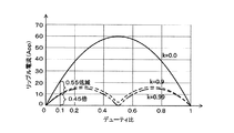
図21は、漏れインダクタンスが2μHの場合のデューティ比とリップル電流との関係を示すグラフである。図の横軸はデューティ比を表し、縦軸はリップル電流(App)を表す。図中の実線、破線及び一点鎖線の夫々は、結合係数kが0.0、0.9及び0.99のときのデューティ比に対するリップル電流の変化特性を示している。上述したように、結合係数kが大きいほどリップル電流が小さくなる傾向が明らかであるため、結合係数kが0.0より大きく0.9より小さい範囲内にあるときの作図は行っていない。 FIG. 21 is a graph showing the relationship between the duty ratio and the ripple current when the leakage inductance is 2 μH. In the figure, the horizontal axis represents the duty ratio, and the vertical axis represents the ripple current (App). Each of the solid line, the broken line, and the alternate long and short dash line in the figure indicates a change characteristic of the ripple current with respect to the duty ratio when the coupling coefficient k is 0.0, 0.9, and 0.99. As described above, since it is clear that the ripple current tends to decrease as the coupling coefficient k increases, no drawing is performed when the coupling coefficient k is in the range of more than 0.0 and less than 0.9.
別の見方をすれば、図21に示す実線は、漏れインダクタンス(実際には自己インダクタンスに相当)が2μHで結合係数kが0である2つの第1インダクタを用いて取得した、0から1までの範囲のデューティ比に対するリップル電流の第1変化特性である。また、図21に示す破線又は一点鎖線は、第1インダクタの自己インダクタンスと同じ大きさの漏れインダクタンスを有しkを−1に近づけた2つの第2インダクタを用いて取得した、0から1までの範囲のデューティ比に対するリップル電流の第2変化特性である。これらの変化特性を一定範囲のデューティ比にわたって逐次比較し、第1変化特性におけるリップル電流に対する第2変化特性におけるリップル電流について最も低い低減率を図21から読み取った値に基づいて算出することができる。 From another point of view, the solid line shown in FIG. 21 is obtained from two first inductors having a leakage inductance (actually equivalent to a self-inductance) of 2 μH and a coupling coefficient k of 0 to 1. It is the 1st change characteristic of the ripple current with respect to the duty ratio of the range. Further, the broken line or the alternate long and short dash line shown in FIG. 21 is obtained using two second inductors having a leakage inductance of the same magnitude as the self-inductance of the first inductor and having k approaching −1. This is a second variation characteristic of the ripple current with respect to the duty ratio in the range. These change characteristics are sequentially compared over a certain range of duty ratios, and the lowest reduction rate of the ripple current in the second change characteristic with respect to the ripple current in the first change characteristic can be calculated based on the value read from FIG. .
この場合、上述したように、リップル電流と漏れインダクタンスとが反比例の関係にあること、及び、コア内の磁束密度を一定にして漏れインダクタンスを低減した場合に低減した割合だけコアの有効断面積が低減されることが分かっている。これらのことから、図21から読み取って算出した低減率だけ第2インダクタの漏れインダクタンスを低減することによってリップル電流が増大する割合と、kを0から0.99にすることによってリップル電流が低減される割合とを相殺させることができる。このようにして、結合係数kが0のときよりもインダクタのリップル電流を増加させない範囲でコア内の磁束密度を変えずにコアのサイズを低減することができる。 In this case, as described above, the ripple current and the leakage inductance are in an inversely proportional relationship, and the effective cross-sectional area of the core is reduced by the reduced ratio when the magnetic flux density in the core is constant and the leakage inductance is reduced. It has been found to be reduced. From these facts, the ripple current is increased by reducing the leakage inductance of the second inductor by the reduction rate calculated by reading from FIG. 21, and the ripple current is reduced by changing k from 0 to 0.99. Can be offset. In this way, the core size can be reduced without changing the magnetic flux density in the core in a range where the ripple current of the inductor is not increased compared to when the coupling coefficient k is 0.
より具体的に、例えば図21でデューティ比が0.1から0.7まで変化する場合、結合係数kを0から0.99に近づけたときにリップル電流が低減される割合が最も小さいのは、デューティ比が0.1のときであり、このときの低減率は0.55である。換言すれば、デューティ比が0.1のときは、kを0から0.99にすることによってリップル電流が0.45倍にしか低減されず、その他のデューティ比ではリップル電流がより大きく低減されて0.45倍より小さくなる。よって、漏れインダクタンスを、2μHの0.45倍である0.9μHに低減し、且つ結合係数kを0.99にすることにより、0.1から0.7までの範囲のデューティ比について、kが0のときよりもリップル電流を増加させないようにできる。そして、漏れインダクタンスを0.45倍(低減率は0.55)に低減することによって、コア内の磁束密度を変えずにコアのサイズ(有効断面積)を0.45倍にすることができる。
More specifically, for example, when the duty ratio changes from 0.1 to 0.7 in FIG. 21, the ratio that the ripple current is reduced when the coupling coefficient k approaches 0 to 0.99 is the smallest. When the duty ratio is 0.1, the reduction rate at this time is 0.55. In other words, when the duty ratio is 0.1, the ripple current is reduced only to 0.45 times by changing k from 0 to 0.99, and the ripple current is greatly reduced at other duty ratios. Less than 0.45 times. Therefore, by reducing the leakage inductance to 0.9 μH, which is 0.45
次に、漏れインダクタンスを低減し、且つkを0から0.99にしたことによるリップル電流への影響について説明する。
図22は、漏れインダクタンスの低減前後におけるデューティ比とリップル電流との関係を示すグラフである。図の横軸はデューティ比を表し、縦軸はリップル電流(App)を表す。図中の実線は、漏れインダクタンス(漏れL)が2μH、且つk=0のときのデューティ比に対するリップル電流の変化特性を示している。この実線は、図21における実線と全く同じものである。また、破線は、漏れインダクタンスが0.9μH、且つk=0.99のときのデューティ比に対するリップル電流の変化特性を示している。
Next, the influence on the ripple current by reducing the leakage inductance and changing k from 0 to 0.99 will be described.
FIG. 22 is a graph showing the relationship between the duty ratio and the ripple current before and after the leakage inductance is reduced. In the figure, the horizontal axis represents the duty ratio, and the vertical axis represents the ripple current (App). The solid line in the figure shows the change characteristic of the ripple current with respect to the duty ratio when the leakage inductance (leakage L) is 2 μH and k = 0. This solid line is exactly the same as the solid line in FIG. Also, the broken line indicates the change characteristic of the ripple current with respect to the duty ratio when the leakage inductance is 0.9 μH and k = 0.99.
破線で示されるリップル電流が、デューティ比が0.5のときに略0の極小となり、0及び0.5の間と、0.5及び1の間とで極大となる曲線を描くのは、図3及び4の場合と同様である。図22によれば、漏れインダクタンスを2μHから0.9μHに低減し、且つkを0から0.99にした場合であっても、少なくとも0.1から0.7までのデューティ比の範囲にわたってリップル電流の増大が抑制されている。 The ripple current indicated by the broken line draws a curve having a minimum of about 0 when the duty ratio is 0.5, and a maximum between 0 and 0.5 and between 0.5 and 1. The same as in the case of FIGS. According to FIG. 22, even when the leakage inductance is reduced from 2 μH to 0.9 μH and k is changed from 0 to 0.99, the ripple is at least over a duty ratio range from 0.1 to 0.7. The increase in current is suppressed.
次に、コアのサイズが低減される効果の確認結果について説明する。
図23は、漏れインダクタンスが0.9μHの場合の結合コイルについて実測したコアの体積を示す図表である。ここでは、コアを介して2つのインダクタを結合させて漏れインダクタンスを0.9μHにした結合コイルA、B、C及びDの4種類について、結合係数が夫々0.78、0.86、0.96及び0.98となるように試作し、コアの体積を測定してコアのサイズの低減効果を実際に確認した。
Next, the confirmation result of the effect of reducing the core size will be described.
FIG. 23 is a chart showing the core volume actually measured for the coupling coil when the leakage inductance is 0.9 μH. Here, for the four types of coupling coils A, B, C, and D in which two inductors are coupled through a core to have a leakage inductance of 0.9 μH, the coupling coefficients are 0.78, 0.86, 0. Trials were made to be 96 and 0.98, and the volume of the core was measured to actually confirm the effect of reducing the core size.
実測の結果、結合コイルA、B、C及びD夫々のコアの体積が、22cm3 、24cm3 、23cm3 及び21cm3 であった。一方、比較の基準となる漏れインダクタンスが2.0μHでk=0の基準結合コイルについては、コアの体積が38cm3 であった。これらの結果より、kが0.78から0.98までの広い範囲にわたって、コアのサイズが十分に低減される効果があると言える。 As a result of the measurement, the volumes of the cores of the coupling coils A, B, C, and D were 22 cm 3 , 24 cm 3 , 23 cm 3, and 21 cm 3 , respectively. On the other hand, for the reference coupling coil having a leakage inductance of 2.0 μH and k = 0 as a reference for comparison, the core volume was 38 cm 3 . From these results, it can be said that the core size is sufficiently reduced over a wide range of k from 0.78 to 0.98.
最後に、結合コイルA、B、C及びD夫々を用いた場合のリップル電流について説明する。
図24は、基準結合コイルを用いた場合のリップル電流の波形を示すグラフであり、図25、26、27及び28の夫々は、結合コイルA、B、C及びDを用いた場合のリップル電流の波形を示すグラフである。各図の横軸は時間(t)を表し、縦軸はインダクタ21又は22の電流(A)を表す。図24から28までの夫々で横軸の基準となる5μsの時間スケールと、縦軸の基準となる20Aの電流スケールとを夫々の図中の適当な箇所に示す。測定条件は、入力電圧が24V、出力電流が概ね70A、周波数が80kHz、デューティ比が0.6である。
Finally, the ripple current when using each of the coupling coils A, B, C and D will be described.
FIG. 24 is a graph showing the ripple current waveform when the reference coupling coil is used, and FIGS. 25, 26, 27 and 28 show the ripple current when the coupling coils A, B, C and D are used. It is a graph which shows the waveform. The horizontal axis of each figure represents time (t), and the vertical axis represents the current (A) of the
ここでは電流振幅の大きさに意味があるため、図24から28までの夫々では、各結合コイルに含まれる2つのインダクタのリップル電流の波形を区別せずに示してある。これらの図では、2つのリップル電流の波形の位相が、互いにπだけずれていることが把握される。そして、図25から28までの夫々に示すリップル電流が、図24に示すリップル電流と同等以下に抑制されていることが確認できる。 Since the magnitude of the current amplitude is significant here, the waveforms of the ripple currents of the two inductors included in each coupling coil are shown without distinction in each of FIGS. In these figures, it is understood that the phases of the two ripple current waveforms are shifted from each other by π. Then, it can be confirmed that the ripple current shown in each of FIGS. 25 to 28 is suppressed to be equal to or less than the ripple current shown in FIG.
なお、本実施形態1にあっては、図21を用いてkを0から0.99(実際は−0.99)に近づけたときのリップル電流の低減率を算出したが、必ずしもkを0.99まで近づける必要はない。上述の説明より、kを1に(実際には−1に)近づけるほどリップル電流が低減される割合が大きくなることが明らかであり、リップル電流が低減される割合が大きいほどコア20のサイズを低減できる割合が大きくなる。
In the first embodiment, the reduction rate of ripple current when k is approximated from 0 to 0.99 (actually −0.99) is calculated using FIG. It is not necessary to get close to 99. From the above description, it is clear that the rate at which the ripple current is reduced increases as k is closer to 1 (actually -1), and the size of the
以上のように本実施形態1によれば、制御部50aが電圧変換回路1aのFET11及び12を交互にオン/オフし、コア20に巻回されて互いに磁気を打ち消し合うインダクタ21及び22夫々に流れる電流をFET11及び12でスイッチングすることにより、電圧変換回路1aに入力された電圧が変換されて出力される。インダクタ21及び22は、漏れインダクタンスLe1及びLe2と密接に関係する結合係数kが0.99≧k≧0.78(実際には−0.99≦k≦−0.78)の範囲内にある。
As described above, according to the first embodiment, the
つまり、2つのインダクタ間の結合係数kが0のときよりもインダクタ21及び22のリップル電流を増加させない範囲で、従来(特許文献2に記載された−0.4<k≦−0.1)よりもkを−1に近づけることができ、kを−1に近づけるほど、kが0のときの自己インダクタンスより小さい漏れインダクタンスLe1及びLe2夫々を有するインダクタ21及び22が適用できる。
従って、漏れインダクタンスLe1及びLe2の低減に応じてコア20のサイズが低減されることと併せて、磁気相殺するインダクタ21及び22が巻回されたコア20のサイズを低減することが可能となる。
That is, in the range in which the ripple current of the
Accordingly, the size of the
また、実施形態1によれば、インダクタ21及び22夫々に流れる電流を0.1≦D≦0.7の範囲のデューティ比Dでスイッチングする。
従って、従来(特許文献1に記載されたD<0.5、又は特許文献2に記載された0.05≦D≦0.40)よりも高いデューティ比に対応可能であり、同じ入力電圧に対して高い出力電圧を得ることが可能となる。
According to the first embodiment, the currents flowing through the
Therefore, it is possible to cope with a duty ratio higher than conventional (D <0.5 described in
更に、実施形態1によれば、結合係数kが0である2つの第1インダクタを用いて取得した、0から1までの範囲のデューティ比に対するリップル電流の第1変化特性と、第1インダクタの自己インダクタンスと同じ大きさの漏れインダクタンスを有しkを−1に近づけた2つの第2インダクタを用いて取得した、0から1までの範囲のデューティ比に対するリップル電流の第2変化特性とを、0.1から0.7までの範囲のデューティ比にわたって逐次比較し、比較結果に基づいて算出したリップル電流の低減率によって、インダクタ21及び22夫々の漏れインダクタンスLe1及びLe2を決定する。
従って、kを−1に近づけることによるリップル電流の低減率と、漏れインダクタンスLe1及びLe2を低減することによるリップル電流の増加率とが相殺されるため、漏れインダクタンスLe1及びLe2の低減に応じてコア20のサイズを低減することが可能となる。
Furthermore, according to the first embodiment, the first change characteristic of the ripple current with respect to the duty ratio in the range from 0 to 1 obtained by using the two first inductors having the coupling coefficient k of 0, the first inductor A second variation characteristic of the ripple current with respect to the duty ratio in the range from 0 to 1, obtained by using two second inductors having a leakage inductance of the same magnitude as the self-inductance and having k close to −1, Sequential comparison is performed over a duty ratio ranging from 0.1 to 0.7, and the leakage inductances Le1 and Le2 of the
Accordingly, the ripple current reduction rate by bringing k closer to −1 cancels out the ripple current increase rate by reducing the leakage inductances Le1 and Le2, so that the cores are reduced according to the reduction of the leakage inductances Le1 and Le2. The size of 20 can be reduced.
更にまた、実施形態1によれば、第1及び第2変化特性を0.1から0.7までの範囲のデューティ比にわたって逐次比較し、第1変化特性におけるリップル電流に対する第2変化特性におけるリップル電流について最も低い低減率(=0.45)を算出し、算出した低減率で第2インダクタの漏れインダクタンスの大きさを低減し、大きさを低減した漏れインダクタンスを、インダクタ21及び22夫々の漏れインダクタンスLe1及びLe2と決定する。
従って、0.1から0.7までの範囲のデューティ比についてワーストケースで保証されるリップル電流の低減率が算出されるため、同じ低減率で第2インダクタの漏れインダクタンスの大きさを低減してインダクタ21及び22夫々の漏れインダクタンスLe1及びLe2と決定した場合に、0.1から0.7までの範囲のデューティ比に対するリップル電流が、2つの第1インダクタを用いたときのリップル電流を超えないようにすることが可能となる。
Furthermore, according to the first embodiment, the first and second change characteristics are sequentially compared over a duty ratio ranging from 0.1 to 0.7, and the ripple in the second change characteristic with respect to the ripple current in the first change characteristic. The lowest reduction rate (= 0.45) is calculated for the current, the magnitude of the leakage inductance of the second inductor is reduced by the calculated reduction rate, and the reduced leakage inductance is set to the leakage of each of the
Therefore, since the reduction rate of the ripple current guaranteed in the worst case is calculated for the duty ratio in the range from 0.1 to 0.7, the magnitude of the leakage inductance of the second inductor is reduced with the same reduction rate. When the leakage inductances Le1 and Le2 of the
(実施形態2)
実施形態1が、電圧変換回路1aで電源2の電圧を降圧する形態であるのに対し、実施形態2は、電圧変換回路で電源2の電圧を昇圧する形態である。
図29は、実施形態2に係る電圧変換装置の構成例を示すブロック図である。電圧変換装置は、外部の電源2から供給された電圧を昇圧して外部の負荷3に供給する電圧変換回路1bと、該電圧変換回路1bによる電圧の変換を制御する制御部50bとを備える。電源2及び負荷3夫々には、コンデンサ31及び32が並列に接続されている。
(Embodiment 2)
The first embodiment is a mode in which the voltage of the
FIG. 29 is a block diagram illustrating a configuration example of the voltage conversion device according to the second embodiment. The voltage conversion device includes a
電圧変換回路1bは、コア20に巻回されて電源2からの電流による磁気を打ち消し合うインダクタ21及び22と、電源2からインダクタ21及び22夫々に流れる電流をスイッチングするFET11及び12とを有する。インダクタ21及び22の一端は、電源2のプラス側に接続されている。インダクタ21の他端は、FET11のドレイン及びダイオード41のアノードに接続されている。インダクタ22の他端は、FET12のドレイン及びダイオード42のアノードに接続されている。FET11及び12のゲートは、制御部50bに接続されている。ダイオード41及び42のカソードは、負荷3の一端に接続されている。電源2のマイナス側と、FET11及び12のソースと、負荷3の他端とは、共通の接地電位に接続されている。
The
制御部50bは、FET11及び12夫々のゲートに位相がπだけ異なる駆動信号を与えることにより、FET11及び12を交互にオン/オフする。その他、実施形態1に対応する箇所には同様の符号を付してその説明を省略する。
The
上述の構成にてインダクタ21及び22に流れるリップル電流(以下、混乱のない限り単にリップル電流という)について説明する。
図30は、実施形態2に係る電圧変換装置におけるFET11及び12の駆動信号と各部に流れる電流とのタイミング関係を示すタイミングチャートである。図6に示す6つのタイミングチャートは、何れも同一の時間軸(t)を横軸にしてあり、図の上段から順に、FET11の駆動信号、FET12の駆動信号、インダクタ21に流れる電流、インダクタ22に流れる電流、ダイオード41の順電流、及びダイオード42の順電流を示してある。インダクタ21及び22夫々に流れる電流の変動成分がリップル電流である。制御部50bがFET11及び12及び22夫々をオンするデューティ比(以下、混乱のない限り単にデューティ比と言う)は、例として略30%である。
The ripple current flowing in the
FIG. 30 is a timing chart showing a timing relationship between the drive signals of the
各信号及び各電流の周期はTである。最初の1周期にてFET11及び12夫々の駆動信号が立ち上がる時刻をt0及びt2とし、夫々の駆動信号が立ち下がる時刻をt1及びt3とする。時刻t0から1周期後の時刻をt4とする。FET11及び12の駆動信号は互いに位相がπだけずれている。即ち、時刻t0から時刻t2までの時間はT/2に相当する。
The period of each signal and each current is T. The times when the drive signals of the
時刻t0からt1までの間では、FET11がオンして電源2からインダクタ21に電流が流れる。この間、電源2からインダクタ21にエネルギーが注入されるため、インダクタ21の電流が増加する。一方のFET12はオフしているが、インダクタ21に流れる電流を打ち消すようにインダクタ22に電流が誘起されるため、インダクタ22の電流が時間の経過と共に増加する。この電流は、ダイオード42を介してコンデンサ32及び負荷3に流れる。
Between time t0 and time t1, the
時刻t1からt2までの間では、FET11がオフし、インダクタ21に流れる電流がダイオード41とコンデンサ32及び負荷3とを介して還流する。また、インダクタ22に流れる電流は、依然としてダイオード42を介してコンデンサ32及び負荷3に流れる。この間、電源2からインダクタ21及び22にエネルギーが注入されないため、インダクタ21及び22の電流が共に減少する。
Between the times t1 and t2, the
時刻t2からt3までの間では、FET12がオンして電源2からインダクタ22に電流が流れる。この間にインダクタ22に流れる電流の増加分は、時刻t0からt1までの間におけるインダクタ21の電流の増加分と同等である。一方のFET11はオフしているが、インダクタ22に流れる電流を打ち消すようにインダクタ21に電流が誘起されるため、インダクタ21の電流が時間の経過と共に増加する。この電流は、ダイオード41を介してコンデンサ32及び負荷3に流れる。
Between time t2 and t3, the
時刻t3からt4までの間では、FET12がオフし、インダクタ22に流れる電流がダイオード42とコンデンサ32及び負荷3とを介して還流する。また、インダクタ21に流れる電流は、依然としてダイオード41を介してコンデンサ32及び負荷3に流れる。この間、電源2からインダクタ21及び22にエネルギーが注入されないため、インダクタ21及び22の電流が共に減少する。時刻t4以降の周期における各信号及び各電流の変化は、時刻t0からt4までの周期におけるものと同様である。
Between time t3 and time t4, the
ここで、インダクタ21及び22間の磁気結合がない場合、即ちインダクタ21及び22間の結合係数kが0の場合を想定すると、時刻t0からt1までの間にインダクタ21に流れる電流の増加分ΔiLは、以下の式(8)で表される。時刻t1からt4までの間にインダクタ21に流れる電流の減少分は、式(8)と絶対値が同じで符号が異なっている。
Here, assuming that there is no magnetic coupling between the
ΔiL=(Vin/L1)D・T・・・・・・・・・・・・・・・・・・(8)
但し、Vin :電圧変換回路1bの入力電圧(=電源2の電圧)
L1 :インダクタ21の自己インダクタンス
D :制御部50bがFET11をオンするデューティ比
T :FET11の駆動信号の周期
ΔiL = (Vin / L1) D · T (8)
However, Vin: Input voltage of the
L1: Self-inductance of
式(8)により、インダクタ21のリップル電流が、自己インダクタンスL1に反比例し、且つ、デューティ比に比例することが示される。
Equation (8) shows that the ripple current of the
一方、インダクタ21及び22間の結合係数kが0<k<1の範囲内にある場合、インダクタ21のインダクタンス成分のうち、式(8)における自己インダクタンスL1と置き換えられてチョークコイルとして機能する成分は、漏れインダクタンスLe1(図6参照)である。以下、インダクタ21,22又はこれに代わる2つのインダクタに係る漏れインダクタンスを、単に漏れインダクタンスという。式(8)の自己インダクタンスL1を同じ大きさの漏れインダクタンスLe1に置き換えた場合におけるインダクタ21のリップル電流は、図30に示すように、k=0の場合よりも小刻みに増減を繰り返すため、k=0の場合よりも小さくなることが容易に推察される。
On the other hand, when the coupling coefficient k between the
特にkを限りなく1に近付けた場合、デューティ比が0.5のときに、FET11がオンの期間中にインダクタ21に流れる電流と、FET11がオフの期間中にFET12によってインダクタ21に誘起する電流とが一致するようになるため、インダクタ21のリップル電流が限りなく小さくなる。
In particular, when k is as close to 1 as possible, when the duty ratio is 0.5, the current that flows in the
本実施形態2では、実施形態1の場合と同様に、リップル電流と漏れインダクタンスとが反比例の関係にあることが明らかである。また、コア内の磁束密度が一定である場合に、コアの有効断面積と漏れインダクタンスとが比例関係にあるこことも同様である。図示は省略するが、漏れインダクタンスを一定にして結合係数kを1に近づけるほどリップル電流が低減されるのも、実施形態1の場合と同様である。 In the second embodiment, as in the case of the first embodiment, it is clear that the ripple current and the leakage inductance are in an inversely proportional relationship. The same applies to the case where the effective cross-sectional area of the core is proportional to the leakage inductance when the magnetic flux density in the core is constant. Although illustration is omitted, the ripple current is reduced as the coupling coefficient k approaches 1 while keeping the leakage inductance constant, as in the case of the first embodiment.
そこで、実施形態1の図21と同様に、漏れインダクタンスが一定で結合係数kが0及び0.99夫々の場合について、0から1までの範囲のデューティ比に対するリップル電流の第1及び第2変化特性を示すグラフを作図する。作図した第1及び第2変化特性のグラフを0.1から0.7までの範囲のデューティ比にわたって逐次比較し、比較結果に基づいて算出したリップル電流の低減率によって、インダクタ21及び22夫々の漏れインダクタンスLe1及びLe2を決定することができる。
従って、kを−1に近づけることによるリップル電流の低減率と、漏れインダクタンスLe1及びLe2を低減することによるリップル電流の増加率とが相殺されるため、漏れインダクタンスLe1及びLe2の低減に応じてコア20のサイズを低減することが可能となる。
Therefore, as in FIG. 21 of the first embodiment, the first and second changes in the ripple current with respect to the duty ratio in the range from 0 to 1 in the case where the leakage inductance is constant and the coupling coefficient k is 0 and 0.99, respectively. Draw a graph showing the characteristics. The plotted graphs of the first and second change characteristics are sequentially compared over a duty ratio ranging from 0.1 to 0.7, and each of the
Accordingly, the ripple current reduction rate by bringing k closer to −1 cancels out the ripple current increase rate by reducing the leakage inductances Le1 and Le2, so that the cores are reduced according to the reduction of the leakage inductances Le1 and Le2. The size of 20 can be reduced.
なお、実施形態1(又は2)にあっては、電圧変換回路1a(又は1b)を1つだけ備えていたが、電圧変換回路1a(又は1b)の数は1つに限定されず、N個(Nは2以上の自然数)を備えて並列に接続するようにしてもよい。
電圧変換回路1a(又は1b)をN個備える場合、制御部50a(又は50b)が、N個の電圧変換回路1a(又は1b)夫々に含まれるFET11及び12を位相差πで交互にオン/オフすると共に、FET11及び12の何れについてもπ/Nずつ異なる位相でオン/オフする。
In the first embodiment (or 2), only one voltage conversion circuit 1a (or 1b) is provided. However, the number of voltage conversion circuits 1a (or 1b) is not limited to one, and N (N is a natural number of 2 or more) and may be connected in parallel.
When N voltage conversion circuits 1a (or 1b) are provided, the
つまり、N個の電圧変換回路1a(又は1b)に含まれるFET11及び12の全てが2π/Nずつ異なる位相でオン/オフされる。
従って、スイッチング損失をN個の電圧変換回路1a(又は1b)に均等に分散することができると共に、出力に含まれるリップル電流を1/Nに低減することが可能となる。
That is, all of the
Therefore, the switching loss can be evenly distributed to the N voltage conversion circuits 1a (or 1b), and the ripple current included in the output can be reduced to 1 / N.
1a、1b 電圧変換回路
11、12、13、14 FET
20 コア
20a、20b、20c 脚部
21、22 インダクタ
31、32 コンデンサ
41、42 ダイオード
50a、50b 制御部
2 電源
3 負荷
1a, 1b
20
Claims (5)
前記2つのインダクタの漏れインダクタンスの大きさは、前記2つのインダクタの結合係数が0である場合に、前記2つのインダクタに流れるリップル電流を所定の低減率で低減するために必要とされる自己インダクタンスの大きさの1倍未満、且つ0.45倍以上の大きさであり、
前記2つのインダクタの結合係数は、−0.99以上、且つ−0.78以下の範囲内にある電圧変換装置。 A voltage conversion device comprising two inductors wound around a core and magnetically canceling each other, a voltage conversion circuit having a switching element that switches a current flowing through each inductor, and a control unit that alternately turns on and off each switching element. There,
The magnitude of the leakage inductance of the two inductors is the self-inductance required to reduce the ripple current flowing through the two inductors at a predetermined reduction rate when the coupling coefficient of the two inductors is zero. Less than 1 time and 0.45 times or more,
Coupling coefficient of the two inductors, -0.99 or more, and a voltage converter in a -0.78 within the following ranges.
該N個の電圧変換回路同士を並列に接続してあり、
前記制御部は、各電圧変換回路のスイッチング素子をπ/Nずつ異なる位相でオン/オフする
請求項1又は2に記載の電圧変換装置。 N voltage conversion circuits (N is a natural number of 2 or more) are provided,
The N voltage conversion circuits are connected in parallel,
The voltage conversion device according to claim 1, wherein the control unit turns on / off switching elements of each voltage conversion circuit at phases different by π / N.
結合係数が0である2つの第1インダクタと、
該第1インダクタの自己インダクタンスと同じ大きさの漏れインダクタンスを有しており結合係数を−1に近づけた2つの第2インダクタとを用意し、
前記2つのインダクタに代えて前記2つの第1インダクタを接続し、
該第1インダクタに流れるリップル電流について、前記制御部が各スイッチング素子をオンする所定範囲のデューティ比に対する第1変化特性を取得し、
前記2つの第1インダクタに代えて前記2つの第2インダクタを接続し、
該第2インダクタに流れるリップル電流について、前記所定範囲のデューティ比に対する第2変化特性を取得し、
取得した第1及び第2変化特性を比較した結果に基づいてリップル電流の低減率を算出し、
前記第2インダクタの漏れインダクタンスの大きさの低減率を、前記算出したリップル電流の低減率以下の低減率とし、
該低減率となるように前記2つのインダクタの漏れインダクタンスの大きさを決定し、
前記2つの第2インダクタの結合係数を前記2つのインダクタの結合係数にする
漏れインダクタンス決定方法。 A method for determining a leakage inductance of the two inductors in a voltage conversion device in which currents flowing in two inductors wound around a core and magnetically cancel each other are switched by a switching element that is turned on / off by a control unit,
Two first inductors having a coupling coefficient of 0;
Preparing two second inductors having a leakage inductance of the same magnitude as the self-inductance of the first inductor and having a coupling coefficient close to −1;
Connecting the two first inductors instead of the two inductors;
For the ripple current flowing through the first inductor, the control unit obtains a first change characteristic with respect to a duty ratio in a predetermined range for turning on each switching element,
Connecting the two second inductors instead of the two first inductors;
For the ripple current flowing through the second inductor, a second change characteristic with respect to the duty ratio in the predetermined range is acquired,
Calculate the ripple current reduction rate based on the comparison result of the obtained first and second change characteristics,
The reduction rate of the leakage inductance of the second inductor is set to a reduction rate equal to or less than the calculated reduction rate of the ripple current,
Wherein determining the size of the two inductor leakage inductance such that the low decline rate,
A method for determining a leakage inductance , wherein the coupling coefficient of the two second inductors is the coupling coefficient of the two inductors .
前記第2インダクタの漏れインダクタンスの大きさの低減率を、前記算出したリップル電流の低減率と同じ低減率とし、
該低減率となるように前記2つのインダクタの漏れインダクタンスの大きさを決定する
請求項4に記載の漏れインダクタンス決定方法。 The calculation of the reduction rate is to calculate the reduction rate of the ripple current at one duty ratio in which the ripple current is reduced at the lowest rate in the second change property with respect to the first change property,
The reduction rate of the leakage inductance of the second inductor is set to the same reduction rate as the calculated ripple current reduction rate,
The leakage inductance determination method according to claim 4, wherein the magnitude of the leakage inductance of the two inductors is determined so as to achieve the reduction rate .
Priority Applications (5)
| Application Number | Priority Date | Filing Date | Title |
|---|---|---|---|
| JP2016116530A JP6149977B1 (en) | 2016-06-10 | 2016-06-10 | Voltage converter and leakage inductance determination method |
| PCT/JP2017/019827 WO2017212954A1 (en) | 2016-06-10 | 2017-05-29 | Voltage conversion device and leakage inductance determination method |
| CN201780035996.1A CN109314462B (en) | 2016-06-10 | 2017-05-29 | Voltage conversion device and leakage inductance determination method |
| US16/308,736 US10483851B2 (en) | 2016-06-10 | 2017-05-29 | Voltage conversion device and method of deciding leakage inductance |
| EP17810133.3A EP3471250A4 (en) | 2016-06-10 | 2017-05-29 | VOLTAGE CONVERSION DEVICE AND LEAKAGE INDUCTANCE DETERMINATION METHOD |
Applications Claiming Priority (1)
| Application Number | Priority Date | Filing Date | Title |
|---|---|---|---|
| JP2016116530A JP6149977B1 (en) | 2016-06-10 | 2016-06-10 | Voltage converter and leakage inductance determination method |
Publications (2)
| Publication Number | Publication Date |
|---|---|
| JP6149977B1 true JP6149977B1 (en) | 2017-06-21 |
| JP2017221088A JP2017221088A (en) | 2017-12-14 |
Family
ID=59081958
Family Applications (1)
| Application Number | Title | Priority Date | Filing Date |
|---|---|---|---|
| JP2016116530A Active JP6149977B1 (en) | 2016-06-10 | 2016-06-10 | Voltage converter and leakage inductance determination method |
Country Status (5)
| Country | Link |
|---|---|
| US (1) | US10483851B2 (en) |
| EP (1) | EP3471250A4 (en) |
| JP (1) | JP6149977B1 (en) |
| CN (1) | CN109314462B (en) |
| WO (1) | WO2017212954A1 (en) |
Families Citing this family (7)
| Publication number | Priority date | Publication date | Assignee | Title |
|---|---|---|---|---|
| US11695337B2 (en) | 2018-12-21 | 2023-07-04 | Cirrus Logic, Inc. | Current control for a boost converter with dual anti-wound inductor |
| CN113472176B (en) | 2020-03-30 | 2023-03-14 | 台达电子工业股份有限公司 | power conversion system |
| JP7279694B2 (en) * | 2020-08-25 | 2023-05-23 | トヨタ自動車株式会社 | Control device |
| JP7230890B2 (en) * | 2020-08-25 | 2023-03-01 | トヨタ自動車株式会社 | power converter |
| CN113315376A (en) * | 2021-06-21 | 2021-08-27 | 哈尔滨工业大学 | Variable-weight DCDC converter based on current ripple optimization |
| CN118251829A (en) * | 2021-11-12 | 2024-06-25 | 思睿逻辑国际半导体有限公司 | Current Control of Boost Converter with Dual Back-Wound Inductors |
| JP7589678B2 (en) | 2021-12-23 | 2024-11-26 | トヨタ自動車株式会社 | Power System |
Family Cites Families (11)
| Publication number | Priority date | Publication date | Assignee | Title |
|---|---|---|---|---|
| US6362986B1 (en) * | 2001-03-22 | 2002-03-26 | Volterra, Inc. | Voltage converter with coupled inductive windings, and associated methods |
| JP3751306B2 (en) | 2004-02-06 | 2006-03-01 | 本田技研工業株式会社 | DC / DC converter and program |
| US7199695B1 (en) * | 2005-10-25 | 2007-04-03 | Virginia Tech Intellectual Properties, Inc. | Multiphase voltage regulator having coupled inductors with reduced winding resistance |
| EP1835604A1 (en) * | 2006-03-16 | 2007-09-19 | STMicroelectronics S.r.l. | Magnetic core for a coupled multi coil filter inductor |
| HRP20140049T1 (en) | 2007-01-05 | 2014-02-28 | University Of Zürich | Anti-beta-amyloid antibody and uses thereof |
| JP5144284B2 (en) * | 2008-01-16 | 2013-02-13 | 本田技研工業株式会社 | Power conversion circuit |
| JP5049245B2 (en) * | 2008-10-21 | 2012-10-17 | 株式会社豊田中央研究所 | Multi-phase converter for on-vehicle use |
| JP5862918B2 (en) * | 2010-06-23 | 2016-02-16 | トヨタ自動車株式会社 | Multiphase converter and design method of multiphase converter |
| US20120319478A1 (en) * | 2011-06-20 | 2012-12-20 | Volterra Semiconductor Corporation | Dc to dc converter with ripple cancellation |
| JP2015056940A (en) * | 2013-09-11 | 2015-03-23 | 株式会社デンソー | Filter circuit for multiphase power converter and multiphase power converter |
| JP6152828B2 (en) * | 2014-06-06 | 2017-06-28 | 株式会社村田製作所 | Multi-phase DC / DC converter |
-
2016
- 2016-06-10 JP JP2016116530A patent/JP6149977B1/en active Active
-
2017
- 2017-05-29 US US16/308,736 patent/US10483851B2/en active Active
- 2017-05-29 WO PCT/JP2017/019827 patent/WO2017212954A1/en not_active Ceased
- 2017-05-29 CN CN201780035996.1A patent/CN109314462B/en active Active
- 2017-05-29 EP EP17810133.3A patent/EP3471250A4/en active Pending
Also Published As
| Publication number | Publication date |
|---|---|
| US20190149049A1 (en) | 2019-05-16 |
| EP3471250A4 (en) | 2020-01-22 |
| WO2017212954A1 (en) | 2017-12-14 |
| EP3471250A1 (en) | 2019-04-17 |
| US10483851B2 (en) | 2019-11-19 |
| JP2017221088A (en) | 2017-12-14 |
| CN109314462B (en) | 2021-01-05 |
| CN109314462A (en) | 2019-02-05 |
Similar Documents
| Publication | Publication Date | Title |
|---|---|---|
| JP6149977B1 (en) | Voltage converter and leakage inductance determination method | |
| JP6198994B1 (en) | Power converter | |
| US10742123B1 (en) | Low common mode noise transformers and switch-mode DC-DC power converters | |
| JP6271099B1 (en) | DC voltage conversion circuit | |
| CN102356438B (en) | Magnetic device formed with u-shaped core pieces and power converter employing the same | |
| KR100597697B1 (en) | Active Common Mode EM Eye Filter | |
| CN111492568B (en) | Interleaved LLC Resonant Converter | |
| US7183754B2 (en) | DC/DC converter | |
| US9722499B2 (en) | Energy transfer element with capacitor compensated cancellation and balance shield windings | |
| WO2018116437A1 (en) | Power conversion device | |
| WO2018116438A1 (en) | Power conversion device | |
| JPWO2017002550A1 (en) | Power circuit | |
| US20020089863A1 (en) | Switching power supply circuit | |
| JP4124814B2 (en) | Input / output isolated DC-DC converter | |
| US6252383B1 (en) | Buck and boost power converters with non-pulsating input and output terminal currents | |
| JPH06511373A (en) | switching regulator | |
| US6198644B1 (en) | Rectifying/smoothing circuit and double-ended converter | |
| JP2018014841A (en) | Voltage converter, step-down control method of power conversion circuit, step-up control method of power conversion circuit and computer program | |
| US7138787B2 (en) | DC/DC converter | |
| JP6038282B2 (en) | Voltage conversion circuit | |
| JP4105606B2 (en) | Switching power supply | |
| CN112350604A (en) | Resonant converter circuit and resonant converter | |
| JP5959459B2 (en) | DC-DC converter | |
| CN214125178U (en) | Resonant converter circuit and resonant converter | |
| JP2020137320A (en) | Step-down converter |
Legal Events
| Date | Code | Title | Description |
|---|---|---|---|
| A521 | Request for written amendment filed |
Free format text: JAPANESE INTERMEDIATE CODE: A523 Effective date: 20170403 |
|
| TRDD | Decision of grant or rejection written | ||
| A01 | Written decision to grant a patent or to grant a registration (utility model) |
Free format text: JAPANESE INTERMEDIATE CODE: A01 Effective date: 20170425 |
|
| A61 | First payment of annual fees (during grant procedure) |
Free format text: JAPANESE INTERMEDIATE CODE: A61 Effective date: 20170508 |
|
| R150 | Certificate of patent or registration of utility model |
Ref document number: 6149977 Country of ref document: JP Free format text: JAPANESE INTERMEDIATE CODE: R150 |
|
| R250 | Receipt of annual fees |
Free format text: JAPANESE INTERMEDIATE CODE: R250 |
|
| R250 | Receipt of annual fees |
Free format text: JAPANESE INTERMEDIATE CODE: R250 |
|
| R250 | Receipt of annual fees |
Free format text: JAPANESE INTERMEDIATE CODE: R250 |
|
| R250 | Receipt of annual fees |
Free format text: JAPANESE INTERMEDIATE CODE: R250 |
|
| R250 | Receipt of annual fees |
Free format text: JAPANESE INTERMEDIATE CODE: R250 |
|
| R250 | Receipt of annual fees |
Free format text: JAPANESE INTERMEDIATE CODE: R250 |