JP6132082B2 - Semiconductor substrate cleaning method and cleaning system - Google Patents
Semiconductor substrate cleaning method and cleaning system Download PDFInfo
- Publication number
- JP6132082B2 JP6132082B2 JP2012183677A JP2012183677A JP6132082B2 JP 6132082 B2 JP6132082 B2 JP 6132082B2 JP 2012183677 A JP2012183677 A JP 2012183677A JP 2012183677 A JP2012183677 A JP 2012183677A JP 6132082 B2 JP6132082 B2 JP 6132082B2
- Authority
- JP
- Japan
- Prior art keywords
- solution
- semiconductor substrate
- sulfuric acid
- cleaning
- halide
- Prior art date
- Legal status (The legal status is an assumption and is not a legal conclusion. Google has not performed a legal analysis and makes no representation as to the accuracy of the status listed.)
- Expired - Fee Related
Links
Images


Landscapes
- Weting (AREA)
- Cleaning Or Drying Semiconductors (AREA)
Description
本発明は、TiNが少なくとも一部露出している、シリサイド化処理がされた半導体基板を洗浄する半導体基板の洗浄方法および洗浄システムに関する。 The present invention relates to a semiconductor substrate cleaning method and a cleaning system for cleaning a silicided semiconductor substrate in which at least a part of TiN is exposed.
近年、CMOSプロセスではシリサイド抵抗を低減するために、シリサイド材料としてNiやCoを用いたNiSiやCoSiが用いられる。しかし、接合リーク電流の低減のため、NiやCoにPtやPdを5〜10%混入した合金が用いられている。中でも、NiPtを用いた場合は耐熱性の向上と接合リーク電流の抑制効果が期待される。(特許文献1、2参照) In recent years, in order to reduce silicide resistance in a CMOS process, NiSi or CoSi using Ni or Co as a silicide material is used. However, in order to reduce the junction leakage current, an alloy in which 5 to 10% of Pt or Pd is mixed with Ni or Co is used. In particular, when NiPt is used, an improvement in heat resistance and an effect of suppressing junction leakage current are expected. (See Patent Documents 1 and 2)
シリサイド化工程では、合金をSi基板上に製膜後、熱酸化処理を施すことで合金とSiが反応してシリサイドが形成されるが、残留する未反応の合金は除去する必要がある。例えばNiPtシリサイド形成後に未反応のNiPtを除去するため、SPM(硫酸と過酸化水素の混合液)を用いる方法が知られている。(特許文献3、4参照)
また、NiPtを溶解しつつゲート金属(TiNなど)のエッチングを抑える洗浄方法として、王水を用いる方法が知られている。(特許文献4、5参照)
また、硫酸系酸化剤で処理した後に塩酸系酸化剤で処理する方法が提案されている。(特許文献6参照)
In the silicidation step, the alloy is formed on a Si substrate and then subjected to thermal oxidation treatment to react the alloy with Si to form silicide, but it is necessary to remove the remaining unreacted alloy. For example, in order to remove unreacted NiPt after forming NiPt silicide, a method using SPM (mixed solution of sulfuric acid and hydrogen peroxide) is known. (See
Also, a method using aqua regia is known as a cleaning method that suppresses etching of gate metal (TiN or the like) while dissolving NiPt. (See
A method of treating with a hydrochloric acid-based oxidizing agent after treating with a sulfuric acid-based oxidizing agent has been proposed. (See Patent Document 6)
しかし、従来の方法のうちSPMを用いる方法では、過酸化水素の配合比率を高くすればNiPtを溶解することができるが、その際にエッチングしてはいけないTiN(例えばゲート電極として露出)も溶解してしまう。
また、王水を用いる方法では、王水がシリサイド膜を痛めてしまう。
さらに、硫酸系酸化剤で処理した後に塩酸系酸化剤で処理する方法では、二段階で処理するため一剤処理と比較して時間がかかり操作が煩雑になるという問題がある。
However, in the conventional method using SPM, NiPt can be dissolved by increasing the blending ratio of hydrogen peroxide, but TiN that should not be etched (for example, exposed as a gate electrode) is also dissolved. Resulting in.
In the method using aqua regia, aqua regia damages the silicide film.
Furthermore, the method of treating with a sulfuric acid-based oxidant and then treating with a hydrochloric acid-based oxidant has a problem that it takes time and operation becomes complicated as compared with one-agent treatment because it is treated in two stages.
本発明は、上記事情を背景としてなされたものであり、TiNが少なくとも一部露出し、シリサイド化処理がされた半導体基板を洗浄する際に、TiNやシリサイド膜の損傷を抑制しつつ効果的に洗浄を行うことができる半導体基板の洗浄方法および洗浄システムを提供することを目的の一つとする。 The present invention has been made against the background of the above circumstances, and at the time of cleaning a semiconductor substrate where at least part of TiN is exposed and silicidized, it is effective while suppressing damage to TiN and silicide films. An object is to provide a semiconductor substrate cleaning method and a cleaning system capable of performing cleaning.
すなわち、本発明の半導体基板の洗浄方法のうち、第1の本発明は、TiNが少なくとも一部露出し、シリサイド化処理がされた半導体基板を洗浄する方法であって、
酸化剤として少なくとも過硫酸を含む硫酸溶液からなる第1溶液と、一種以上のハロゲン化物イオンを含む第2溶液とを混合して、酸化剤濃度が0.001〜2mol/Lの混合溶液を生成する混合溶液生成工程と、前記混合溶液を前記半導体基板に接触させて該半導体基板を洗浄する基板洗浄工程とを有すること特徴とする。
That is, of the semiconductor substrate cleaning methods of the present invention, the first present invention is a method of cleaning a semiconductor substrate that is at least partially exposed and silicidized,
A first solution composed of a sulfuric acid solution containing at least persulfuric acid as an oxidant and a second solution containing one or more halide ions are mixed to form a mixed solution having an oxidant concentration of 0.001 to 2 mol / L. And a substrate cleaning step of cleaning the semiconductor substrate by bringing the mixed solution into contact with the semiconductor substrate.
第2の本発明の半導体基板の洗浄方法は、前記第1の本発明において、前記混合溶液生成工程が、第1溶液と第2溶液とを前記半導体基板に接触させる前に混合して混合溶液とする工程、または第1溶液と第2溶液とをそれぞれ別経路で供給して前記半導体基板上で互いに混ぜ合わせる工程であることを特徴とする。 The method for cleaning a semiconductor substrate according to a second aspect of the present invention is the method for cleaning a semiconductor substrate according to the first aspect of the present invention, wherein the mixed solution generating step mixes the first solution and the second solution before contacting the semiconductor substrate. Or a step of supplying the first solution and the second solution through different paths and mixing them together on the semiconductor substrate.
第3の本発明の半導体基板の洗浄方法は、前記第1または第2の本発明において、前記ハロゲン化物イオンがフッ化物イオン、塩化物イオン、臭化物イオン、ヨウ化物イオンのいずれかであることを特徴とする。 According to a third aspect of the present invention, there is provided the method for cleaning a semiconductor substrate according to the first or second aspect of the present invention, wherein the halide ion is any one of a fluoride ion, a chloride ion, a bromide ion, and an iodide ion. Features.
第4の本発明の半導体基板の洗浄方法は、前記第1〜第3の本発明のいずれかにおいて、前記半導体基板は前記シリサイド化処理に用いた金属膜を有し、該金属膜が白金を含むことを特徴とする。 According to a fourth aspect of the present invention, there is provided the method for cleaning a semiconductor substrate according to any one of the first to third aspects, wherein the semiconductor substrate has a metal film used for the silicidation treatment, and the metal film is made of platinum. It is characterized by including.
第5の本発明の半導体基板の洗浄方法は、前記第1〜第4の本発明のいずれかにおいて、前記混合溶液において、前記ハロゲン化物イオンの濃度の総和が0.2mmol/L〜2mol/Lであることを特徴とする。 The semiconductor substrate cleaning method according to a fifth aspect of the present invention is the method for cleaning a semiconductor substrate according to any one of the first to fourth aspects of the present invention, wherein the total concentration of the halide ions is 0.2 mmol / L to 2 mol / L in the mixed solution. It is characterized by being.
第6の本発明の半導体基板の洗浄方法は、前記第1〜第5の本発明のいずれかにおいて、前記酸化剤を含む硫酸溶液が、硫酸電解液、硫酸と過酸化水素の混合溶液、硫酸とオゾンの混合溶液からなる群から選ばれる1種以上であることを特徴とする。 According to a sixth aspect of the present invention, there is provided the method for cleaning a semiconductor substrate according to any one of the first to fifth aspects, wherein the sulfuric acid solution containing the oxidizing agent is a sulfuric acid electrolyte, a mixed solution of sulfuric acid and hydrogen peroxide, sulfuric acid. And at least one selected from the group consisting of a mixed solution of ozone and ozone.
第7の本発明の半導体基板の洗浄方法は、前記第1〜第6の本発明のいずれかにおいて、前記混合溶液において、液温を80〜200℃の沸点以下の温度にして前記半導体基板に接触させることを特徴とする。 According to a seventh aspect of the present invention, there is provided a method for cleaning a semiconductor substrate according to any one of the first to sixth aspects of the present invention, wherein the liquid temperature of the mixed solution is set to a temperature equal to or lower than a boiling point of 80 to 200 ° C. It is made to contact.
第8の本発明の半導体基板の洗浄方法は、前記第7の本発明において、80℃以上の前記混合溶液を生成してから5分以内に前記半導体基板に接触させることを特徴とする。 The method for cleaning a semiconductor substrate according to an eighth aspect of the present invention is characterized in that, in the seventh aspect of the present invention, the mixed solution at 80 ° C. or higher is brought into contact with the semiconductor substrate within 5 minutes.
第9の本発明の半導体基板の洗浄方法は、前記第1〜第8の本発明のいずれかにおいて、前記硫酸溶液の濃度が、前記混合溶液において50〜95質量%であることを特徴とする。 According to a ninth aspect of the present invention, there is provided the method for cleaning a semiconductor substrate according to any one of the first to eighth aspects, wherein the concentration of the sulfuric acid solution is 50 to 95% by mass in the mixed solution. .
第10の本発明の半導体基板の洗浄システムは、
TiNが少なくとも一部露出し、シリサイド化処理がされた半導体基板を洗浄する洗浄部と、
前記洗浄部に配置され、洗浄用の溶液を前記洗浄部の半導体基板に送出して接触させる送出部と、
一端が前記送出部に接続され、酸化剤として少なくとも過硫酸を含む硫酸溶液を前記送出部に移送する硫酸溶液移送路と、
一端が前記送出部に接続され、一種以上のハロゲン化物イオンを含むハロゲン化物溶液を前記送出部に移送するハロゲン化物溶液移送路と、を備え、
前記硫酸溶液移送路と前記ハロゲン化物溶液移送路とは途中で合流して共通移送路を形成して前記送出部に接続されていることを特徴とする。
A semiconductor substrate cleaning system according to a tenth aspect of the present invention includes:
A cleaning unit for cleaning the semiconductor substrate in which at least a part of TiN is exposed and silicidized;
A sending unit disposed in the cleaning unit and sending a cleaning solution to and contact the semiconductor substrate of the cleaning unit;
A sulfuric acid solution transfer path, one end of which is connected to the delivery unit and transports a sulfuric acid solution containing at least persulfuric acid as an oxidant to the delivery unit;
A halide solution transport path, one end of which is connected to the delivery unit and transports a halide solution containing one or more halide ions to the delivery unit;
The sulfuric acid solution transfer path and the halide solution transfer path join in the middle to form a common transfer path and are connected to the delivery unit.
第11の本発明の半導体基板の洗浄システムは、前記第10の本発明において、
前記硫酸溶液と前記ハロゲン化物溶液とが前記共通移送路中で混合されて酸化剤濃度0.001〜2mol/Lの混合溶液となるよう構成されていることを特徴とする。
An eleventh aspect of the present invention is a semiconductor substrate cleaning system according to the tenth aspect of the present invention,
The sulfuric acid solution and the halide solution are mixed in the common transfer path to form a mixed solution having an oxidizing agent concentration of 0.001 to 2 mol / L.
第12の本発明の半導体基板の洗浄システムは、前記第10または第11の本発明において、前記共通移送路に介設され、または前記硫酸溶液移送路と前記ハロゲン化物溶液移送路とが接続された混合槽を有し、該混合槽で前記硫酸溶液と前記ハロゲン化物溶液とが混合していることを特徴とする。 A semiconductor substrate cleaning system according to a twelfth aspect of the present invention is the semiconductor substrate cleaning system according to the tenth or eleventh aspect of the present invention, wherein the semiconductor substrate cleaning system is interposed in the common transfer path, or the sulfuric acid solution transfer path and the halide solution transfer path are connected. And the sulfuric acid solution and the halide solution are mixed in the mixing tank.
第13の本発明の半導体基板の洗浄システムは、前記第10〜第12の本発明のいずれかにおいて、前記硫酸溶液移送路における前記共通移送路より上流側、前記ハロゲン化物溶液移送路における前記共通移送路より上流側、前記共通移送路のうち少なくとも1箇所に、溶液を加熱する加熱部が介設されていることを特徴とする。 The semiconductor substrate cleaning system of the thirteenth aspect of the present invention is the semiconductor substrate cleaning system according to any one of the tenth to twelfth aspects of the present invention, wherein the common in the halide solution transfer path is upstream of the common transfer path in the sulfuric acid solution transfer path. A heating unit that heats the solution is interposed in at least one of the common transfer paths upstream from the transfer path.
第14の本発明の半導体基板の洗浄システムは、
TiNが少なくとも一部露出し、シリサイド化処理がされた半導体基板を洗浄する洗浄部と、
前記洗浄部に配置され、酸化剤として少なくとも過硫酸を含む硫酸溶液を前記洗浄部の半導体基板に送出して接触させる硫酸溶液送出部と、
一端が前記硫酸溶液送出部に接続され、前記硫酸溶液を前記硫酸溶液送出部に移送する硫酸溶液移送路と、
前記洗浄部に配置され、一種以上のハロゲン化物イオンを含むハロゲン化物溶液を前記洗浄部の半導体基板に送出して接触させるハロゲン化物溶液送出部と、
一端が前記ハロゲン化物溶液送出部に接続され、前記ハロゲン化物溶液を前記ハロゲン化物溶液送出部に移送するハロゲン化物溶液移送路と、を備え、
前記硫酸溶液送出部と前記ハロゲン化物溶液送出部とは、前記硫酸溶液送出部から送出された前記硫酸溶液と前記ハロゲン化物溶液送出部から送出された前記ハロゲン化物溶液とが前記半導体基板上で混じり合うように配置されていることを特徴とする。
A semiconductor substrate cleaning system according to a fourteenth aspect of the present invention includes
A cleaning unit for cleaning the semiconductor substrate in which at least a part of TiN is exposed and silicidized;
A sulfuric acid solution delivery unit disposed in the cleaning unit and sending a sulfuric acid solution containing at least persulfuric acid as an oxidizing agent to the semiconductor substrate of the cleaning unit; and
One end is connected to the sulfuric acid solution delivery unit, and a sulfuric acid solution transfer path for transferring the sulfuric acid solution to the sulfuric acid solution delivery unit,
A halide solution delivery unit disposed in the cleaning unit and configured to send and contact a halide solution containing one or more halide ions to the semiconductor substrate of the cleaning unit;
One end connected to the halide solution delivery section, and a halide solution transfer path for transferring the halide solution to the halide solution delivery section,
The sulfuric acid solution delivery unit and the halide solution delivery unit are a mixture of the sulfuric acid solution delivered from the sulfuric acid solution delivery unit and the halide solution delivered from the halide solution delivery unit on the semiconductor substrate. It is arrange | positioned so that it may fit.
第15の本発明の半導体基板の洗浄システムは、前記第14の本発明において、
前記硫酸溶液と前記ハロゲン化物溶液とが前記洗浄部の半導体基板上で互いに混ざり合い酸化剤濃度0.001〜2mol/Lの混合溶液となるよう構成されていることを特徴とする。
The semiconductor substrate cleaning system of the fifteenth aspect of the present invention is the fourteenth aspect of the present invention,
The sulfuric acid solution and the halide solution are mixed with each other on the semiconductor substrate of the cleaning unit to form a mixed solution having an oxidizing agent concentration of 0.001 to 2 mol / L.
第16の本発明の半導体基板の洗浄システムは、前記第14または第15の本発明において、
前記硫酸溶液移送路および前記ハロゲン化物溶液移送路の一方または両方に溶液を加熱する加熱部が介設されていることを特徴とする。
According to a sixteenth aspect of the present invention, there is provided the semiconductor substrate cleaning system according to the fourteenth or fifteenth aspect,
A heating section for heating the solution is interposed in one or both of the sulfuric acid solution transfer path and the halide solution transfer path.
第17の本発明の半導体基板の洗浄システムは、前記第10〜第16の本発明のいずれかにおいて、前記洗浄部が、枚葉式であることを特徴とする。 According to a seventeenth aspect of the present invention, there is provided the semiconductor substrate cleaning system according to any one of the tenth to sixteenth aspects, wherein the cleaning section is a single wafer type.
本発明で洗浄の対象となる半導体基板は、TiNが少なくとも一部露出し、シリサイド化処理がされた半導体基板である。該半導体基板の製造方法は本発明としては特に限定されるものではない。 The semiconductor substrate to be cleaned in the present invention is a semiconductor substrate in which at least a part of TiN is exposed and silicidation is performed. The method for producing the semiconductor substrate is not particularly limited as the present invention.
本発明で用いる第1溶液は、酸化剤として少なくとも過硫酸を含む硫酸溶液であり、硫酸電解液、硫酸と過酸化水素の混合溶液、硫酸とオゾンの混合溶液などを選択することができる。なお、過硫酸としては、ペルオキソ二硫酸とペルオキソ一硫酸が例示され、いずれか一方、または両方が混合したものでもよい。このとき酸化剤としては過硫酸と過硫酸の自己分解に伴って発生する過酸化水素がほぼ全量を占める。
酸化剤は、第1溶液と第2溶液の混合溶液において、0.001〜2mol/Lの濃度となるように混合条件を設定しておく。
酸化剤濃度0.001mol/L未満では洗浄力が不足し、酸化剤濃度が2mol/Lを超過するとエッチングレートが高くなってしまい実用が困難である。
硫酸溶液は、第1溶液と第2溶液の混合溶液において、硫酸濃度が50〜95質量%となるように設定するのが望ましく。80質量%以上とすることが、沸点が高くない、より高温で洗浄できるという理由でより好ましい。ただし含水量が極度に少ないとシリサイド化処理に用いた膜に含まれる金属の溶解効率が下がるので90質量%以下とするのが好ましい。
The first solution used in the present invention is a sulfuric acid solution containing at least persulfuric acid as an oxidizing agent, and a sulfuric acid electrolyte, a mixed solution of sulfuric acid and hydrogen peroxide, a mixed solution of sulfuric acid and ozone, or the like can be selected. Examples of persulfuric acid include peroxodisulfuric acid and peroxomonosulfuric acid, and either one or a mixture of both may be used. At this time, as the oxidant, persulfuric acid and hydrogen peroxide generated by the self-decomposition of persulfuric acid occupy almost the whole amount.
The mixing condition is set so that the oxidizing agent has a concentration of 0.001 to 2 mol / L in the mixed solution of the first solution and the second solution.
When the oxidant concentration is less than 0.001 mol / L, the detergency is insufficient, and when the oxidant concentration exceeds 2 mol / L, the etching rate becomes high and practical use is difficult.
The sulfuric acid solution is desirably set so that the sulfuric acid concentration is 50 to 95% by mass in the mixed solution of the first solution and the second solution. 80 mass% or more is more preferable because the boiling point is not high and cleaning is possible at a higher temperature. However, if the water content is extremely low, the dissolution efficiency of the metal contained in the film used for the silicidation treatment is lowered, so that the content is preferably 90% by mass or less.
第2溶液は、一種以上のハロゲン化物イオンを含む溶液であり、ハロゲン化物イオンとしては、例えば、フッ化物イオン、塩化物イオン、臭化物イオン、ヨウ化物イオンの一種または二種以上が例示される。ハロゲン化物イオンを含む溶液としては、ハロゲン化物イオンの水素酸(HF、HCl、HBr、HI)やその塩(NaCl)の溶液が挙げられる。しかしHBrやHI、I2は着色しやすく、NaClのような塩はNaがウエハ上に残存する恐れがあり、さらにHFは取り扱いに注意を要するため、HClが好ましい。
なお、ハロゲン化物イオンは、第1溶液と第2溶液の混合溶液において、各ハロゲン化物イオン濃度の総和が0.2mmol/L〜2mol/Lとなるように調整するのが望ましい。
The second solution is a solution containing one or more halide ions, and examples of the halide ions include one or more of fluoride ions, chloride ions, bromide ions, and iodide ions. Examples of the solution containing halide ions include a solution of a halide ion hydroacid (HF, HCl, HBr, HI) or a salt thereof (NaCl). However, HBr, HI, and I 2 are easily colored, and salts such as NaCl may cause Na to remain on the wafer. Further, HF requires caution in handling, and HCl is preferable.
The halide ions are preferably adjusted so that the total concentration of each halide ion is 0.2 mmol / L to 2 mol / L in the mixed solution of the first solution and the second solution.
第1溶液と第2溶液とを混合する位置は、洗浄する半導体基板上であっても、洗浄より事前に予め2液をライン混合か或いは混合槽などの槽中で混合しておいてもよい。
要は、半導体基板を洗浄する際に両液を混合して半導体基板に接触させるものであればよい。この場合は生成した錯化剤がシリサイド化用に形成した膜と接触するまでに消費することを避けるために2液混合して液温80℃以上とした後、5分(好ましくは3分)以内に洗浄に供することが好ましい。なお、第1溶液として硫酸電解液を用いる場合、電解セルや電解液貯留槽やその循環ラインにハロゲン化物イオンが混入すると、電解により多量のハロゲンガスが発生するため、硫酸電解液が使用側に供給される過程で混合することが望ましい。
Even if the position which mixes a 1st solution and a 2nd solution is on the semiconductor substrate to wash | clean, you may mix two liquids beforehand in tanks, such as line mixing or a mixing tank, before washing | cleaning. .
In short, what is necessary is just to mix both solutions and to contact a semiconductor substrate when wash | cleaning a semiconductor substrate. In this case, in order to avoid consumption of the complexing agent produced until it comes into contact with the film formed for silicidation, the two liquids are mixed to a liquid temperature of 80 ° C. or higher, and then 5 minutes (preferably 3 minutes). It is preferable to use for washing. In addition, when using a sulfuric acid electrolyte as the first solution, if halide ions are mixed into the electrolytic cell, the electrolyte reservoir, or the circulation line thereof, a large amount of halogen gas is generated by electrolysis. It is desirable to mix in the supplied process.
半導体基板に接触させる混合溶液は、液温を80℃以上、好ましくは100℃以上の温度にして前記半導体基板に接触させるのが望ましい。
これは、80℃未満では洗浄能力が不足であり、100℃以上であれば洗浄能力はほぼ十分だからである。一方、液温の上限は200℃以下の沸点以下の温度とすることができるが、エネルギー効率やエッチングレートの点から160℃以下の沸点以下の温度であることがより好ましい。
なお、液温を調整する場合、半導体基板に混合した溶液を接触させる際に上記温度を有するものとする。
The mixed solution brought into contact with the semiconductor substrate is desirably brought into contact with the semiconductor substrate at a liquid temperature of 80 ° C. or higher, preferably 100 ° C. or higher.
This is because the cleaning ability is insufficient at less than 80 ° C., and the cleaning ability is almost sufficient at 100 ° C. or higher. On the other hand, the upper limit of the liquid temperature can be set to a temperature not higher than the boiling point of 200 ° C. or lower, but is more preferably a temperature not higher than the boiling point of 160 ° C. or lower from the viewpoint of energy efficiency and etching rate.
In addition, when adjusting liquid temperature, it shall have the said temperature when contacting the solution mixed with the semiconductor substrate.
また、洗浄はバッチ式でも枚葉式でも構わないが、接触効率の点で枚葉式の方がより好ましい。 The cleaning may be either batch type or single wafer type, but the single wafer type is more preferable in terms of contact efficiency.
すなわち、本発明によれば、酸化剤として少なくとも過硫酸を含む硫酸溶液とハロゲン化物イオンを含む溶液とが混じり合い、酸化剤濃度が0.001〜2mol/Lの状態で半導体基板に接触することで、TiNやシリサイド膜を傷めることなく半導体基板を効果的に洗浄することができる。 That is, according to the present invention, a sulfuric acid solution containing at least persulfuric acid as an oxidant is mixed with a solution containing halide ions, and contacts the semiconductor substrate in a state where the oxidant concentration is 0.001 to 2 mol / L. Thus, the semiconductor substrate can be effectively cleaned without damaging the TiN or silicide film.
(実施形態1)
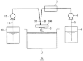
以下に、本発明の一実施形態の半導体基板洗浄システム1を図1に基づいて説明する。
半導体基板洗浄システム1は、本発明の洗浄部に相当する枚葉式洗浄機2と、酸化剤を含む硫酸溶液を貯留する硫酸溶液貯留槽4と、ハロゲン化合物イオンを含む溶液を貯留するハロゲン化物溶液貯留槽10とを備えている。
枚葉式洗浄機2は基板支持台3を備えており、基板支持台3は、図示しない駆動装置によって回転駆動が可能になっている。枚葉式洗浄機2は、本発明の洗浄部に相当し、基板支持台3に支持された半導体基板100に洗浄用の溶液を送出する送出ノズル30を備えている。送出ノズル30は、本発明の送出部に相当し、洗浄用の溶液を半導体基板100に噴霧、滴下、または流下する。なお、滴下、流下では圧力を与えて半導体基板100に溶液を吹き付けるものであってもよい。
(Embodiment 1)
Below, the semiconductor substrate cleaning system 1 of one Embodiment of this invention is demonstrated based on FIG.
A semiconductor substrate cleaning system 1 includes a single
The single
硫酸溶液貯留槽4は、硫酸溶液移送路5が接続されている。また、ハロゲン化物溶液貯留槽10は、ハロゲン化物溶液移送路11が接続されている。硫酸溶液移送路5は、送液ポンプ6が介設され、その下流側に、移送される硫酸溶液を一過式で加熱するヒーター7が介設されている。ヒーター7は本発明の加熱部に相当する。ハロゲン化物溶液移送路11は送液ポンプ12が介設されている。
The sulfuric acid
硫酸溶液移送路5とハロゲン化物溶液移送路11とは、ヒーター7および送液ポンプ12の下流側で合流して共通する共通移送路20を構成しており、共通移送路20の下流端は送出ノズル30に接続されている。
The sulfuric acid
次に、半導体基板洗浄システム1を使用した半導体基板洗浄方法を以下に説明する。
先ず、TiNが少なくとも一部露出し、シリサイド化処理がされた半導体基板100を基板支持台3に支持する。半導体基板100は、例えば、メタルゲート電極が積層されたシリコン基板上に金属膜を形成し、前記シリコン基板に対してアニール処理を行ってシリコン基板上に白金などの貴金属を含むシリサイド層を形成したものを用いることができる。金属膜は、白金などの貴金属を含むものであってもよい。
但し、本発明としては半導体基板100の製造方法がこれに限定されるものではなく、TiNが少なくとも一部露出し、シリサイド化処理をされた半導体基板であれば洗浄対象とすることができる。
Next, a semiconductor substrate cleaning method using the semiconductor substrate cleaning system 1 will be described below.
First, at least a part of TiN is exposed, and the
However, the manufacturing method of the
なお、本実施形態で好適な対象例は、メタルゲート電極やサイドウォールが形成されているなどTiNが少なくとも一部露出し、その膜厚が60nm以下(好ましくは30nm以下)、シリサイド層の厚さが60nm以下(好ましくは25nm以下)、ゲート幅が45nm以下(好ましくは30nm以下)のケースである。ただし、本発明で対象となる半導体基板がこれに限定されるものではない。 A suitable target example in the present embodiment is that at least a part of TiN is exposed, such as a metal gate electrode or a sidewall, and the thickness thereof is 60 nm or less (preferably 30 nm or less), and the thickness of the silicide layer. Is 60 nm or less (preferably 25 nm or less) and the gate width is 45 nm or less (preferably 30 nm or less). However, the semiconductor substrate which is the subject of the present invention is not limited to this.
また、硫酸溶液貯留槽4には、後述するハロゲン化物溶液との混合により得られる溶液において、少なくとも過硫酸を含む酸化剤の濃度が0.001〜2mol/Lとなり、硫酸濃度が50〜95質量%となるように調整した硫酸溶液を収容する。
硫酸溶液貯留槽4に貯留する酸化剤を含む硫酸溶液は、本発明の第1溶液に相当する。
酸化剤を含む硫酸溶液は、バッチ式に硫酸溶液貯留槽4に貯留するものでもよく、また、消費量に相応して連続して酸化剤を含む硫酸溶液を補充するものであってもよい。過硫酸を含む硫酸溶液は、好適には硫酸電解液によって効率よく補充することができる。
Further, in the sulfuric acid
The sulfuric acid solution containing the oxidizing agent stored in the sulfuric acid
The sulfuric acid solution containing the oxidizing agent may be stored in the sulfuric acid
一方、ハロゲン化物溶液貯留槽10には、上記過硫酸を含む硫酸溶液との混合によって得られる溶液において、ハロゲン化物イオンの濃度の総和が0.2mmol/L〜2mol/Lとなるように調整する。ハロゲン化物溶液としては、ハロゲン化物イオンの水素酸(HF、HCl、HBr、HI)やその塩(NaClなど)の溶液を好適に用いることができる。ハロゲン化物溶液貯留槽10に収容されるハロゲン化物溶液は、本発明の第2溶液に相当する。
On the other hand, the halide
半導体基板100の洗浄に際しては、基板支持台3を回転駆動して半導体基板100を回転支持するとともに、硫酸溶液貯留槽4内の過硫酸を含む硫酸溶液を送液ポンプ6によって硫酸溶液移送路5を通して所定の流量で送液し、ハロゲン化物溶液貯留槽10内のハロゲン化物溶液を送液ポンプ12によってハロゲン化物溶液移送路11を通して所定の流量で送液する。両液は、両移送路が合流する共通移送路20で混合される。なお、硫酸溶液の流量と、ハロゲン化物溶液の流量とは、両液が混合された際に所定の混合比となり、かつ混合された溶液の流量が所定量となるように設定する。
また、本実施形態では硫酸溶液移送路5で移送される、過硫酸を含む硫酸溶液は、合流前にヒーター7で一過式に加熱する。加熱温度は、ハロゲン化物溶液の混合後、半導体基板100に接触させるときに、液温が80〜200℃で沸点以下の温度となるように調整する。なお、本実施形態では、硫酸溶液のみを加熱しているが、ハロゲン化物溶液移送路11にヒーターを設けてハロゲン化物溶液を加熱するようにしてもよく、共通移送路20で加熱するようにしてもよい。
When cleaning the
In the present embodiment, the sulfuric acid solution containing persulfuric acid transferred by the sulfuric acid
過硫酸を含む硫酸溶液とハロゲン化物イオンを含むハロゲン化物溶液とは、混合溶液において、酸化剤の濃度が0.001〜2mol/L、ハロゲン化物イオンの総和の濃度が0.2mmol/L〜2mol/L、硫酸濃度が50〜95質量%、液温が80〜200℃で沸点以下の状態で、送出ノズル30から送出されて半導体基板100に接触し、半導体基板100の洗浄が行われる。なお、過硫酸を含む硫酸溶液とハロゲン化物溶液とは、混合状態で液温80℃以上の時点から5分以内(好ましくは3分)以内に半導体基板100に接触するように送液速度および共通移送路20の長さを定めるのが望ましい。
この際に、TiNのエッチングレートが450Å/min以下、好ましくは150Å/min以下になるような条件で洗浄し、また洗浄時間が120秒以内程度、好ましくは100秒以内になるような条件で洗浄をするのが望ましい。
In the mixed solution, the sulfuric acid solution containing persulfuric acid and the halide solution containing halide ions have a concentration of oxidant of 0.001 to 2 mol / L and a total concentration of halide ions of 0.2 mmol / L to 2 mol. / L, the sulfuric acid concentration is 50 to 95% by mass, the liquid temperature is 80 to 200 ° C. and the boiling point or lower, the liquid is delivered from the
At this time, the cleaning is performed under such a condition that the etching rate of TiN is 450 Å / min or less, preferably 150 Å / min or less, and the cleaning time is about 120 seconds or less, preferably 100 seconds or less. It is desirable to do.
上記洗浄における作用の詳細を以下に説明する。
〈NiPt剥離〉
推定されるメカニズムは以下の通りである。
過硫酸とハロゲン化物イオンが反応することにより、Ptを溶解しかつPtと錯体を作りやすい錯化剤の硫酸ハロゲン化合物が生成されると考えられる。その硫酸ハロゲン化合物をシリコン基板表面のNiPtシリサイド残渣に接触されることで、NiのみでなくPtを強く溶解し、NiPt残渣を完全に除去することができる。特許文献6に示されるように、半導体基板に対する硫酸の接触とハロゲン化物イオンとの接触とを別工程にすると過硫酸とハロゲン化物イオンが接触しないため過硫酸とハロゲン化合物による錯化剤が生成されず除去効率が低い。
また、過硫酸を含む硫酸溶液と、ハロゲン化物溶液とを洗浄の直前に混合することで、錯化剤が洗浄に利用される前に消費されてしまうのを回避することができる。
The details of the operation in the cleaning will be described below.
<NiPt peeling>
The presumed mechanism is as follows.
By reacting persulfuric acid with halide ions, it is considered that a halogenated sulfate compound, which is a complexing agent that dissolves Pt and easily forms a complex with Pt, is generated. By contacting the halogenated sulfuric acid compound with the NiPt silicide residue on the silicon substrate surface, not only Ni but also Pt is strongly dissolved, and the NiPt residue can be completely removed. As shown in
Further, by mixing the sulfuric acid solution containing persulfuric acid and the halide solution immediately before washing, it is possible to avoid that the complexing agent is consumed before being used for washing.
〈TiNエッチング抑制〉
本混合溶液を用いることにより、酸化剤濃度を抑えつつNiPt除去することができ、メタルゲート電極やサイドウォールなどTiNのエッチングを抑制することができる。
<TiN etching suppression>
By using this mixed solution, NiPt can be removed while suppressing the oxidant concentration, and etching of TiN such as metal gate electrodes and sidewalls can be suppressed.
〈シリサイドダメージの抑制〉
また、TiNのエッチングを抑えながらNiPtを剥離できる溶液として王水があるが、王水はシリサイドを傷める原因とされるハロゲン化物イオンが高濃度であるためシリサイドを傷めてしまう。しかし本実施形態の混合溶液はハロゲン化物イオンを低濃度に抑えることでシリサイドのダメージを抑制できる。
<Suppression of silicide damage>
There is aqua regia as a solution that can remove NiPt while suppressing etching of TiN, but aqua rejuvenation damages silicide due to a high concentration of halide ions that cause damage to silicide. However, the mixed solution of this embodiment can suppress silicide damage by suppressing halide ions to a low concentration.
〈処理時間の短縮〉
本実施形態は、一段で処理することにより、二段で処理するより時間が短縮でき装置や操作も単純になる。
<Reduction of processing time>
In the present embodiment, processing in one stage can shorten the time compared with processing in two stages, and the apparatus and operation become simple.
(実施形態2)
次に、実施形態2を図2に基づいて説明する。なお、実施形態1と同様の構成については同一の符号を付しており、その説明を省略または簡略化する。
半導体基板洗浄システム1aは、枚葉式洗浄機2と硫酸溶液貯留槽4とハロゲン化物溶液貯留槽10とを備えている。
(Embodiment 2)
Next,
The semiconductor
硫酸溶液貯留槽に4は硫酸溶液移送路5が接続され、ハロゲン化物溶液貯留槽10には、ハロゲン化物溶液移送路11が接続されている。硫酸溶液移送路5とハロゲン化物溶液移送路11とは合流し、共通する共通移送路21を構成しており、共通移送路21の下流端は送出ノズル30に接続されている。硫酸溶液移送路5には共通移送路21の上流側に送液ポンプ6が介設され、ハロゲン化物溶液移送路11には共通移送路21の上流側に送液ポンプ12が介設されている。また、共通移送路21には、送液される混合溶液を加熱するヒーター7が介設されている。
The sulfuric acid
次に、半導体基板洗浄システム1aを使用した半導体基板洗浄方法を以下に説明する。
先ず、実施形態1と同様に半導体基板100を枚葉式洗浄機2の基板支持台3に支持する。
Next, a semiconductor substrate cleaning method using the semiconductor
First, the
硫酸溶液貯留槽4には、実施形態1と同様に混合溶液の状態で、酸化剤の濃度が0.001〜2mol/Lとなり、硫酸濃度が50〜95質量%となるように調整した硫酸溶液を収容する。ハロゲン化物溶液貯留槽10には、実施形態1と同様に混合溶液の状態で、ハロゲン化物イオンの濃度の総和が0.2mmol/L〜2mol/Lとなるように調整する。
In the sulfuric acid
半導体基板100の洗浄に際しては、基板支持台3を回転駆動して半導体基板100を回転支持するとともに、硫酸溶液貯留槽4内の過硫酸を含む硫酸溶液を送液ポンプ6によって硫酸溶液移送路5を通じて所定の流量で送液し、ハロゲン化物溶液貯留槽10内のハロゲン化物溶液を送液ポンプ12によってハロゲン化物溶液移送路11を通じて所定の流量で送液し、両移送路が合流する共通移送路21で両液を混合する。なお、硫酸溶液の流量と、ハロゲン化物溶液の流量とは、前記実施形態1と同様に、両液が混合された際に所定の混合比となり、かつ混合された溶液の流量が所定量となるように設定する。
また、共通移送路21を移送する、過硫酸を含む硫酸溶液とハロゲン化物溶液との混合溶液は、ヒーター7で一過式に加熱し、半導体基板100に接触させるときに、液温が80〜200℃で沸点以下の温度となるように調整する。なお本実施形態では加熱温度もこの範囲の温度とすることができる。
When cleaning the
Further, the mixed solution of the sulfuric acid solution containing persulfuric acid and the halide solution, which is transferred through the
過硫酸を含む硫酸溶液とハロゲン化物イオンを含むハロゲン化物溶液とは、混合された溶液において、酸化剤の濃度が0.001〜2mol/L、ハロゲン化物イオンの総和の濃度が0.2mmol/L〜2mol/L、硫酸濃度が50〜95質量%、液温が80〜200℃で沸点以下の状態で、送出ノズル30から送出されて半導体基板100に接触し、半導体基板100の洗浄が行われる。なお、過硫酸を含む硫酸溶液とハロゲン化物溶液とは、共通移送路21の混合溶液が液温80℃以上になった時点から5分以内(好ましくは3分以内)に半導体基板100に接触するように送液速度および共通移送路21の長さを定めるのが望ましい。
この際に、TiNのエッチングレートが450Å/min以下、好ましくは150Å/min以下になるような条件で洗浄し、また洗浄時間が120秒以内程度、好ましくは100秒以内になるような条件で洗浄をするのが望ましい。
In the mixed solution, the sulfuric acid solution containing persulfuric acid and the halide solution containing halide ions had a concentration of oxidant of 0.001 to 2 mol / L and a total concentration of halide ions of 0.2 mmol / L. In the state of ˜2 mol / L, sulfuric acid concentration of 50 to 95 mass%, liquid temperature of 80 to 200 ° C. and below boiling point, the
At this time, the cleaning is performed under such a condition that the etching rate of TiN is 450 Å / min or less, preferably 150 Å / min or less, and the cleaning time is about 120 seconds or less, preferably 100 seconds or less. It is desirable to do.
(実施形態3)
次に、実施形態3の半導体基板洗浄システム1bを図3に基づいて説明する。なお、実施形態1と同様の構成については同一の符号を付しており、その説明を省略または簡略化する。
この実施形態では、硫酸溶液移送路5とハロゲン化物溶液移送路11とを混合槽25に接続し、混合槽25に接続された共通移送路22を送出ノズル30に接続したものである。混合槽25には混合槽ヒーター26が設けられ、共通移送路22にはヒーター7が介設されている。
(Embodiment 3)
Next, the semiconductor
In this embodiment, the sulfuric acid
この実施形態3では、混合槽25で所定の混合比が得られるように、硫酸溶液貯留槽4から送液ポンプ6によって硫酸溶液移送路5を通して過硫酸を含む硫酸溶液を混合槽25に移送し、ハロゲン化物溶液貯留槽10から送液ポンプ12によってハロゲン化物溶液移送路11を通してハロゲン化物溶液を混合槽25に移送する。
混合槽25内の溶液は、酸化剤の濃度が0.001〜2mol/L、ハロゲン化物イオンの総和の濃度が0.2mmol/L〜2mol/L、硫酸濃度が50〜95質量%となるように調整する。調整は、硫酸溶液貯留槽4内の硫酸溶液の酸化剤濃度、硫酸濃度および送液量、ハロゲン化物溶液貯留槽10内のハロゲン化物イオンの濃度および送液量によって行うことができる。
In
The solution in the
混合槽25の溶液は、必要に応じて混合槽ヒーター26で加熱し、送液ポンプ23によって共通移送路22を通して移送する。この際にヒーター7によって混合溶液を加熱し、
半導体基板100に接触させる際の液温が80〜200℃で沸点以下となるように調整する。この際に、溶液が混合槽ヒーター26で加熱されていれば、ヒーター7の加熱負担を軽減できる。但し、混合槽25での加熱温度は、過硫酸や硫酸ハロゲン化合物の自己分解が進行しすぎないように、50℃以下に抑えるのが望ましい。混合溶液が半導体基板100と接触することにより前記実施形態と同様に半導体基板100の洗浄が行われる。
この際に、TiNのエッチングレートが450Å/min以下、好ましくは150Å/min以下になるような条件で洗浄し、また洗浄時間が120秒以内程度、好ましくは100秒以内になるような条件で洗浄をするのが望ましい。
The solution in the
It adjusts so that the liquid temperature at the time of making it contact with the
At this time, the cleaning is performed under such a condition that the etching rate of TiN is 450 Å / min or less, preferably 150 Å / min or less, and the cleaning time is about 120 seconds or less, preferably 100 seconds or less. It is desirable to do.
なお、過硫酸を含む硫酸溶液とハロゲン化物溶液とは、混合槽25で混合された後、ヒーター7に通液され加熱開始した時点から5分以内(好ましくは3分以内)に半導体基板100に接触するように、混合槽25の槽容量や、混合槽25からの送液速度および共通移送路22の長さを定めるのが望ましい。ヒーター7では、急速加熱によって溶液が通液され加熱開始されると直ちに80℃以上の液温となる。
The sulfuric acid solution containing persulfuric acid and the halide solution are mixed in the
(実施形態4)
上記各実施形態1〜3では、過硫酸を含む硫酸溶液とハロゲン化物溶液とを混合した後、移送し、半導体基板100に接触させるものとして説明したが、過硫酸を含む硫酸溶液とハロゲン化物溶液とが別経路で移送され、半導体基板100上で混じり合うようにしてもよい。
この実施形態4の半導体基板洗浄システム1cを図4に基づいて説明する。なお、実施形態1と同様の構成については同一の符号を付しており、その説明を省略または簡略化する。
(Embodiment 4)
In each of the first to third embodiments described above, the sulfuric acid solution containing persulfuric acid and the halide solution are mixed and then transferred and brought into contact with the
A semiconductor
この実施形態では、実施形態1〜3と同様に硫酸溶液貯留槽4とハロゲン化物溶液貯留槽10とを備え、硫酸溶液貯留槽4に収容される過硫酸を含む硫酸溶液の酸化剤濃度、硫酸濃度が調整され、ハロゲン化物溶液移送路11に収容されるハロゲン化物イオンの総イオン濃度が調整される。
In this embodiment, as in the first to third embodiments, the sulfuric acid
硫酸溶液貯留槽4に接続された硫酸溶液移送路5の下流端には硫酸溶液送出ノズル31が接続され、ハロゲン化物溶液貯留槽10に接続されたハロゲン化物溶液移送路11の下流端にはハロゲン化物溶液送出ノズル32が接続されている。硫酸溶液送出ノズル31とハロゲン化物溶液送出ノズル32とは、送出されたそれぞれの溶液が半導体基板100上で効率よく混じり合うように取付け位置や取付け角度を設定するのが望ましい。
また、所定の混合比が得られるように硫酸溶液移送路5を移送される過硫酸を含む硫酸溶液と、ハロゲン化物溶液移送路11を移送されるハロゲン化物溶液とが所定の混合比で混じり合い、送出される溶液の総量が所定量となるように、各溶液の流量を定める。
この実施形態においても、半導体基板100上に送液された各溶液は半導体基板100上で混じり合い、前記各実施形態と同様に半導体基板100の洗浄を良好に行うことができる。この形態では、第1溶液と第2溶液とが混合する工程と、混合の溶液を半導体基板に接触させて洗浄する工程とが同一工程で行われる。
A sulfuric acid
Further, the sulfuric acid solution containing persulfuric acid transferred through the sulfuric acid
Also in this embodiment, the solutions sent onto the
なお、上記各実施形態では、洗浄部として枚葉式のものを説明したが、本発明としてはバッチ式のものであってもよい。枚葉式の洗浄部は、半導体基板1枚ずつを洗浄するものであり、特には洗浄用の溶液を半導体基板に噴霧、滴下、流下等するものが例示される。バッチ式の洗浄部は、1枚または複数枚の半導体基板を洗浄するものであり、特には、洗浄用の溶液を貯液し、ここに半導体基板を所定時間浸漬するものが例示される。 In each of the above embodiments, a single wafer type was described as the cleaning unit, but a batch type may be used as the present invention. The single wafer cleaning unit is for cleaning each semiconductor substrate one by one, and in particular, one that sprays, drops, flows down, etc. a cleaning solution on the semiconductor substrate is exemplified. The batch-type cleaning unit is for cleaning one or a plurality of semiconductor substrates, and in particular, one that stores a cleaning solution and immerses the semiconductor substrate in a predetermined time is exemplified.
以下に、本発明の実施例および比較例を示す。なお、実施例および比較例では、図5に概略を示す半導体基板洗浄システム1dまたは図3、図4に示す半導体基板洗浄システムを用いて洗浄を行った。図5の装置は、基本構成を実施形態1と同様とするものであり、ヒーター7を具備せず硫酸溶液貯留槽4にヒーター8を備えている。なお、各洗浄では、混合液は、加熱および混合がされた後、直ちに(1分以内に)、下記するベタウエハに対し接触する洗浄に供給される。
なお、以下では、NiPt除去率が95%以上を良、95%未満を不良と評価した。
TiNのエッチングレートは、450Å/minを超えるものは、TiNを損傷するものとして評価は不良、450Å/min以下は評価は良となる。
また、シリサイドダメージの有無は、表面粗さRaが1.9μm未満であればダメージなしと評価し、Raが1.9μm以上であればダメージありと評価した。
Examples of the present invention and comparative examples are shown below. In Examples and Comparative Examples, cleaning was performed using the semiconductor
In the following, NiPt removal rates of 95% or more were evaluated as good and less than 95% were evaluated as defective.
When the etching rate of TiN exceeds 450 Å / min, the evaluation is poor as damaging TiN, and when it is 450 Å / min or less, the evaluation is good.
The presence or absence of silicide damage was evaluated as having no damage if the surface roughness Ra was less than 1.9 μm, and evaluated as having damage if Ra was 1.9 μm or more.
(比較例1)
図5の枚葉式洗浄機で、電解硫酸溶液(硫酸濃度80%、酸化剤濃度0.07mol/L)を用いて、(1)シリコンウエハ上にNiPt層が10nm積層したベタウエハおよび(2)シリコンウエハ上にTiN層が600nm積層したベタウエハに対して、200ml/minで接触させる洗浄をそれぞれ130℃、100秒間実施した。処理後の溶液をICP−MS(誘導結合プラズマ質量分析装置、以下単にICP−MSと表記する)を用いて成分分析し、溶液中のNi、Pt、Tiの濃度からウエハのNiPtの除去率、TiNのエッチングレートを確認し、ウエハ表面をAFM(原子間力顕微鏡:Atomic Force Microscope、以下単にAFMと表記する)で観察してシリサイドダメージの有無を確認し、表1に結果を示した。
結果、NiPt除去率は50%、TiNエッチングレートは50Å/min、NiPtシリサイドダメージなしであった。
(Comparative Example 1)
In the single wafer cleaning machine of FIG. 5, using an electrolytic sulfuric acid solution (sulfuric acid concentration 80%, oxidizing agent concentration 0.07 mol / L), (1) a solid wafer having a NiPt layer of 10 nm laminated on a silicon wafer, and (2) The solid wafer having a TiN layer of 600 nm laminated on the silicon wafer was cleaned at 130 ° C. for 100 seconds, respectively, at 200 ml / min. The processed solution is subjected to component analysis using ICP-MS (inductively coupled plasma mass spectrometer, hereinafter simply referred to as ICP-MS), and the removal rate of NiPt on the wafer from the concentrations of Ni, Pt, and Ti in the solution, The etching rate of TiN was confirmed, the surface of the wafer was observed with an AFM (Atomic Force Microscope, hereinafter simply referred to as AFM), and the presence or absence of silicide damage was confirmed. Table 1 shows the results.
As a result, the NiPt removal rate was 50%, the TiN etching rate was 50 Å / min, and there was no NiPt silicide damage.
(比較例2)
図5の枚葉式洗浄機で、電解硫酸溶液(硫酸濃度80%、酸化剤濃度0.04mol/L)を用いて、(1)シリコンウエハ上にNiPt層が10nm積層したベタウエハおよび(2)シリコンウエハ上にTiN層が600nm積層したベタウエハに対して200ml/minで接触させる洗浄をそれぞれ130℃、100秒間実施した。処理後の溶液をICP−MSを用いて成分分析し、溶液中のNi、Pt、Tiの濃度からウエハのNiPtの除去率、TiNのエッチングレートを確認し、ウエハ表面をAFMで観察してシリサイドダメージの有無を確認し、表1に示した。
結果、NiPt除去率は40%、TiNエッチングレートは40Å/min、NiPtシリサイドダメージなしであった。
(Comparative Example 2)
5 using an electrolytic sulfuric acid solution (sulfuric acid concentration 80%, oxidizing agent concentration 0.04 mol / L), (1) a solid wafer in which a NiPt layer is laminated to 10 nm on a silicon wafer, and (2) Washing was performed at 130 ° C. for 100 seconds with a solid wafer having a TiN layer of 600 nm stacked on a silicon wafer at 200 ml / min. Component analysis of the treated solution using ICP-MS was performed, the NiPt removal rate of the wafer and the etching rate of TiN were confirmed from the concentrations of Ni, Pt, and Ti in the solution, and the wafer surface was observed by AFM to silicide The presence or absence of damage was confirmed and shown in Table 1.
As a result, the NiPt removal rate was 40%, the TiN etching rate was 40 Å / min, and there was no NiPt silicide damage.
(比較例3)
図5の枚葉式洗浄機で、酸化剤濃度が2.14mol/L、硫酸濃度が67%であるSPM溶液(H2SO4:H2O2=2:1)を用いて、(1)シリコンウエハ上にNiPt層が10nm積層したベタウエハおよび(2)シリコンウエハ上にTiN層が600nm積層したベタウエハに対して200ml/minで接触させる洗浄をそれぞれ130℃、100秒間実施した。処理後の溶液をICP−MSを用いて成分分析し、溶液中のNi、Pt、Tiの濃度からウエハのNiPtの除去率、TiNのエッチングレートを確認し、ウエハ表面をAFMで観察してシリサイドダメージの有無を確認し、表1に示した。
結果、NiPt除去率は100%、TiNエッチングレートは600Å/min、NiPtシリサイドダメージなしであった。
(Comparative Example 3)
5 using an SPM solution (H 2 SO 4 : H 2 O 2 = 2: 1) having an oxidant concentration of 2.14 mol / L and a sulfuric acid concentration of 67%. Cleaning was performed at 130 ° C. for 100 seconds, respectively, at 200 ml / min on a solid wafer in which a NiPt layer was laminated to 10 nm on a silicon wafer and (2) a solid wafer in which a TiN layer was laminated to 600 nm on a silicon wafer. Component analysis of the treated solution using ICP-MS was performed, the NiPt removal rate of the wafer and the etching rate of TiN were confirmed from the concentrations of Ni, Pt, and Ti in the solution, and the wafer surface was observed by AFM to silicide The presence or absence of damage was confirmed and shown in Table 1.
As a result, the NiPt removal rate was 100%, the TiN etching rate was 600 Å / min, and there was no NiPt silicide damage.
(比較例4)
図5の枚葉式洗浄機で、酸化剤濃度が0.71mol/L、硫酸濃度が80%であるSPM溶液(H2SO4:H2O2=4:1)を用いて、(1)シリコンウエハ上にNiPt層が10nm積層したベタウエハおよび(2)シリコンウエハ上にTiN層が600nm積層したベタウエハに対して200ml/minで接触させる洗浄をそれぞれ130℃、100秒間実施した。処理後の溶液をICP−MSを用いて成分分析し、溶液中のNi、Pt、Tiの濃度からウエハのNiPtの除去率、TiNのエッチングレートを確認し、ウエハ表面をAFMで観察してシリサイドダメージの有無を確認し、表1に示した。
結果、TiNエッチングレートは350Å/min、NiPtシリサイドダメージなしであったもののNiPt除去率は80%であり不十分であった。
(Comparative Example 4)
Using the SPM solution (H 2 SO 4: H 2 O 2 = 4: 1) having an oxidizing agent concentration of 0.71 mol / L and a sulfuric acid concentration of 80% in the single wafer cleaning machine of FIG. Cleaning was performed at 130 ° C. for 100 seconds with a solid wafer in which a NiPt layer was laminated to 10 nm on a silicon wafer and (2) a solid wafer in which a TiN layer was laminated to 600 nm on a silicon wafer at 200 ml / min. Component analysis of the treated solution using ICP-MS was performed, the NiPt removal rate of the wafer and the etching rate of TiN were confirmed from the concentrations of Ni, Pt, and Ti in the solution, and the wafer surface was observed by AFM to silicide The presence or absence of damage was confirmed and shown in Table 1.
As a result, although the TiN etching rate was 350 Å / min and there was no NiPt silicide damage, the NiPt removal rate was 80%, which was insufficient.
(比較例5)
図5の枚葉式洗浄機で、酸化剤濃度が0.41mol/L、硫酸濃度が83%であるSPM溶液(H2SO4:H2O2=5:1)を用いて、(1)シリコンウエハ上にNiPt層が10nm積層したベタウエハおよび(2)シリコンウエハ上にTiN層が600nm積層したベタウエハに対して200ml/minで接触させる洗浄をそれぞれ130℃、100秒間実施した。処理後の溶液をICP−MSを用いて成分分析し、溶液中のNi、Pt、Tiの濃度からウエハのNiPtの除去率、TiNのエッチングレートを確認し、ウエハ表面をAFMで観察してシリサイドダメージの有無を確認し、表1に示した。
結果、TiNエッチングレートは250Å/min、NiPtシリサイドダメージなしであったもののNiPt除去率は60%であり不十分であった。
(Comparative Example 5)
5 using an SPM solution (H 2 SO 4 : H 2 O 2 = 5: 1) having an oxidant concentration of 0.41 mol / L and a sulfuric acid concentration of 83%, (1 Cleaning was performed at 130 ° C. for 100 seconds, respectively, at 200 ml / min on a solid wafer in which a NiPt layer was laminated to 10 nm on a silicon wafer and (2) a solid wafer in which a TiN layer was laminated to 600 nm on a silicon wafer. Component analysis of the treated solution using ICP-MS was performed, the NiPt removal rate of the wafer and the etching rate of TiN were confirmed from the concentrations of Ni, Pt, and Ti in the solution, and the wafer surface was observed by AFM to silicide The presence or absence of damage was confirmed and shown in Table 1.
As a result, although the TiN etching rate was 250 min / min and there was no NiPt silicide damage, the NiPt removal rate was 60%, which was insufficient.
(比較例6)
図5の枚葉式洗浄機で、酸化剤濃度が0.18mol/L、硫酸濃度が90%であるSPM溶液(H2SO4:H2O2=10:1)を用いて、(1)シリコンウエハ上にNiPt層が10nm積層したベタウエハおよび(2)シリコンウエハ上にTiN層が600nm積層したベタウエハに対して200ml/minで接触させる洗浄をそれぞれ130℃、100秒間実施した。処理後の溶液をICP−MSを用いて成分分析し、溶液中のNi、Pt、Tiの濃度からウエハのNiPtの除去率、TiNのエッチングレートを確認し、ウエハ表面をAFMで観察してシリサイドダメージの有無を確認し、表1に示した。
結果、TiNエッチングレートは120Å/min、NiPtシリサイドダメージなしであったもののNiPt除去率は50%であり不十分であった。
(Comparative Example 6)
5 using an SPM solution (H 2 SO 4 : H 2 O 2 = 10: 1) having an oxidant concentration of 0.18 mol / L and a sulfuric acid concentration of 90%. Cleaning was performed at 130 ° C. for 100 seconds, respectively, at 200 ml / min on a solid wafer in which a NiPt layer was laminated to 10 nm on a silicon wafer and (2) a solid wafer in which a TiN layer was laminated to 600 nm on a silicon wafer. Component analysis of the treated solution using ICP-MS was performed, the NiPt removal rate of the wafer and the etching rate of TiN were confirmed from the concentrations of Ni, Pt, and Ti in the solution, and the wafer surface was observed by AFM to silicide The presence or absence of damage was confirmed and shown in Table 1.
As a result, although the TiN etching rate was 120 Å / min and there was no NiPt silicide damage, the NiPt removal rate was 50%, which was insufficient.
(比較例7)
図5の枚葉式洗浄機で、王水を用いて、(1)シリコンウエハ上にNiPt層が10nm積層したベタウエハおよび(2)シリコンウエハ上にTiN層が600nm積層したベタウエハに対して200ml/minで接触させる洗浄をそれぞれ80℃、200秒間実施した。処理後の溶液をICP−MSを用いて成分分析し、溶液中のNi、Pt、Tiの濃度からウエハのNiPtの除去率、TiNのエッチングレートを確認し、ウエハ表面をAFMで観察してシリサイドダメージの有無を確認し、表1に示した。
結果、NiPt除去率は100%、TiNエッチングレートは40Å/min、NiPtシリサイドダメージありであった。
(Comparative Example 7)
In the single wafer cleaning machine of FIG. 5, using aqua regia, (1) a solid wafer having a NiPt layer of 10 nm laminated on a silicon wafer and (2) a solid wafer having a TiN layer of 600 nm laminated on a silicon wafer, 200 ml / Washing with contact for min was performed at 80 ° C. for 200 seconds, respectively. Component analysis of the treated solution using ICP-MS was performed, the NiPt removal rate of the wafer and the etching rate of TiN were confirmed from the concentrations of Ni, Pt, and Ti in the solution, and the wafer surface was observed by AFM to silicide The presence or absence of damage was confirmed and shown in Table 1.
As a result, the NiPt removal rate was 100%, the TiN etching rate was 40 Å / min, and there was NiPt silicide damage.
(比較例8)
図5の枚葉式洗浄機で、酸化剤濃度が0.41mol/L、硫酸濃度が83%であるSPM(H2SO4:H2O2=5:1)を用いて、(1)シリコンウエハ上にNiPt層が10nm積層したベタウエハおよび(2)シリコンウエハ上にTiN層が600nm積層したベタウエハに対して200ml/minで接触させる洗浄をそれぞれ130℃、50秒間実施した。その後、図5の枚様式洗浄機で、王水を用いて、前記SPMで洗浄した前記ベタウエハに対して200ml/minで接触させる洗浄をそれぞれ50℃、50秒間実施した。処理後の溶液をICP−MSを用いて成分分析し、溶液中のNi、Pt、Tiの濃度からウエハのNiPtの除去率、TiNのエッチングレートを確認し、ウエハ表面をAFMで観察してシリサイドダメージの有無を確認し、表1に示した。
結果、NiPt除去率は100%、TiNエッチングレートは150Å/min、NiPtシリサイドダメージなしであったが、処理時間が2工程で170秒かかった。
(Comparative Example 8)
In the single wafer cleaning machine of FIG. 5, using SPM (H 2 SO 4 : H 2 O 2 = 5: 1) having an oxidizing agent concentration of 0.41 mol / L and a sulfuric acid concentration of 83%, (1) Cleaning was performed at 130 ° C. for 50 seconds with a solid wafer having a NiPt layer of 10 nm laminated on a silicon wafer and (2) a solid wafer having a TiN layer of 600 nm laminated on the silicon wafer at 200 ml / min. Thereafter, cleaning was performed at 50 ° C. for 50 seconds with the single wafer cleaning machine of FIG. 5 using aqua regia to contact the solid wafer cleaned with the SPM at 200 ml / min. Component analysis of the treated solution using ICP-MS was performed, the NiPt removal rate of the wafer and the etching rate of TiN were confirmed from the concentrations of Ni, Pt, and Ti in the solution, and the wafer surface was observed by AFM to silicide The presence or absence of damage was confirmed and shown in Table 1.
As a result, the NiPt removal rate was 100%, the TiN etching rate was 150 Å / min, and there was no NiPt silicide damage, but the processing time took 170 seconds in two steps.
(比較例9)
図5の枚葉式洗浄機で、電解硫酸溶液(硫酸濃度30%、酸化剤濃度0.07mol/L)を用いて、(1)シリコンウエハ上にNiPt層が10nm積層したベタウエハおよび(2)シリコンウエハ上にTiN層が600nm積層したベタウエハに対して、200ml/minで接触させる洗浄をそれぞれ130℃、100秒間実施した。処理後の溶液をICP−MS(誘導結合プラズマ質量分析装置、以下単にICP−MSと表記する)を用いて成分分析し、溶液中のNi、Pt、Tiの濃度からウエハのNiPtの除去率、TiNのエッチングレートを確認し、ウエハ表面をAFM(原子力顕微鏡:Atomic Force Microscope、以下単にAFMと表記する)で観察してシリサイドダメージの有無を確認し、表1に結果を示した。
結果、NiPt除去率は80%、TiNエッチングレートは300Å/min、NiPtシリサイドダメージなしであった。
(Comparative Example 9)
In the single wafer cleaning machine of FIG. 5, using an electrolytic sulfuric acid solution (
As a result, the NiPt removal rate was 80%, the TiN etching rate was 300 Å / min, and there was no NiPt silicide damage.
(比較例10)
図5の枚葉式洗浄機で、電解硫酸溶液(硫酸濃度80%、酸化剤濃度0.07mol/L)を用いて、(1)シリコンウエハ上にNiPt層が10nm積層したベタウエハおよび(2)シリコンウエハ上にTiN層が600nm積層したベタウエハに対して、200ml/minで接触させる洗浄をそれぞれ40℃、100秒間実施した。処理後の溶液をICP−MSを用いて成分分析し、溶液中のNi、Pt、Tiの濃度からウエハのNiPtの除去率、TiNのエッチングレートを確認し、ウエハ表面をAFMで観察してシリサイドダメージの有無を確認し、表1に結果を示した。
結果、NiPt除去率は20%、TiNエッチングレートは10Å/min、NiPtシリサイドダメージなしであった。
(Comparative Example 10)
In the single wafer cleaning machine of FIG. 5, using an electrolytic sulfuric acid solution (sulfuric acid concentration 80%, oxidizing agent concentration 0.07 mol / L), (1) a solid wafer having a NiPt layer of 10 nm laminated on a silicon wafer, and (2) A solid wafer having a TiN layer of 600 nm stacked on a silicon wafer was cleaned at 40 ° C. for 100 seconds at 200 ml / min. Component analysis of the treated solution using ICP-MS was performed, the NiPt removal rate of the wafer and the etching rate of TiN were confirmed from the concentrations of Ni, Pt, and Ti in the solution, and the wafer surface was observed by AFM to silicide The presence or absence of damage was confirmed, and the results are shown in Table 1.
As a result, the NiPt removal rate was 20%, the TiN etching rate was 10 Å / min, and there was no NiPt silicide damage.
(比較例11)
図5の枚葉式洗浄機で、酸化剤濃度が2.14mol/L、硫酸濃度が67%である130℃のSPM(H2SO4:H2O2=2:1)にHCl濃度が35%のHCl水溶液を体積比2500:7で混合した。混合溶液のCl濃度は0.027mol/Lであり、混合による液温、酸化剤濃度は殆ど変化がなく、混合前と同等である。この混合液を用いて、(1)シリコンウエハ上にNiPt層が10nm積層したベタウエハおよび(2)シリコンウエハ上にTiN層が600nm積層したベタウエハに対し200ml/minで接触させる洗浄をそれぞれ130℃、100秒間実施した。処理後の溶液をICP−MSを用いて成分分析し、溶液中のNi、Pt、Tiの濃度からウエハのNiPtの除去率、TiNのエッチングレートを確認し、ウエハ表面をAFMで観察してシリサイドダメージの有無を確認し、表1に示した。
結果、NiPt除去率は100%、TiNエッチングレートは620Å/min、NiPtシリサイドダメージなしであった。
(Comparative Example 11)
In the single wafer cleaning machine of FIG. 5, the HCl concentration in the SPM (H 2 SO 4 : H 2 O 2 = 2: 1) at 130 ° C. where the oxidant concentration is 2.14 mol / L and the sulfuric acid concentration is 67%. A 35% HCl aqueous solution was mixed at a volume ratio of 2500: 7. The Cl concentration of the mixed solution is 0.027 mol / L, and the liquid temperature and the oxidizing agent concentration due to mixing are almost unchanged, and are the same as before mixing. Using this mixed solution, cleaning was performed at 130 ° C. at 200 ml / min for each of (1) a solid wafer having a 10 nm NiPt layer laminated on a silicon wafer and (2) a solid wafer having a 600 nm TiN layer laminated on a silicon wafer. Conducted for 100 seconds. Component analysis of the treated solution using ICP-MS was performed, the NiPt removal rate of the wafer and the etching rate of TiN were confirmed from the concentrations of Ni, Pt, and Ti in the solution, and the wafer surface was observed by AFM to silicide The presence or absence of damage was confirmed and shown in Table 1.
As a result, the NiPt removal rate was 100%, the TiN etching rate was 620 Å / min, and there was no NiPt silicide damage.
(実施例1)
図5の枚葉式洗浄機で、130℃の電解硫酸溶液(硫酸濃度80%、酸化剤濃度0.07mol/L)に、HCl濃度が35%のHCl水溶液を体積比2500:7で混合した。混合溶液のCl濃度は0.027mol/Lであり、混合による液温、硫酸濃度、酸化剤濃度は殆ど変化がなく、混合前と同等である(以下同様)。前記混合溶液を用いて、(1)シリコンウエハ上にNiPt層が10nm積層したベタウエハおよび(2)シリコンウエハ上にTiN層が600nm積層したベタウエハに対してそれぞれ200ml/minで接触させる洗浄をそれぞれ130℃、100秒間実施した。処理後の溶液をICP−MSを用いて成分分析し、溶液中のNi、Pt、Tiの濃度からウエハのNiPtの除去率、TiNのエッチングレートを確認し、ウエハ表面をAFMで観察してシリサイドダメージの有無を確認し、表1に示した。
結果、NiPt除去率は100%、TiNエッチングレートは60Å/min、NiPtシリサイドダメージなしであった。
Example 1
In the single wafer washer shown in FIG. 5, an aqueous HCl solution having an HCl concentration of 35% was mixed with an electrolytic sulfuric acid solution (sulfuric acid concentration 80%, oxidizing agent concentration 0.07 mol / L) at 130 ° C. at a volume ratio of 2500: 7. . The Cl concentration of the mixed solution is 0.027 mol / L, and the liquid temperature, the sulfuric acid concentration, and the oxidizing agent concentration by mixing are almost unchanged and the same as before mixing (the same applies hereinafter). Using the mixed solution, cleaning is performed at a rate of 200 ml / min for each of (1) a solid wafer having a 10 nm NiPt layer stacked on a silicon wafer and (2) a solid wafer having a 600 nm TiN layer stacked on a silicon wafer. C., 100 seconds. Component analysis of the treated solution using ICP-MS was performed, the NiPt removal rate of the wafer and the etching rate of TiN were confirmed from the concentrations of Ni, Pt, and Ti in the solution, and the wafer surface was observed by AFM to silicide The presence or absence of damage was confirmed and shown in Table 1.
As a result, the NiPt removal rate was 100%, the TiN etching rate was 60 Å / min, and there was no NiPt silicide damage.
(実施例2)
図5の枚葉式洗浄機で、130℃の電解硫酸溶液(硫酸濃度80%、酸化剤濃度0.07mol/L)にHCl濃度が35%のHCl水溶液を体積比2500:7で混合した混合溶液(Cl濃度0.027mol/L)を用いて、(1)シリコンウエハ上にNiPt層が10nm積層したベタウエハおよび(2)シリコンウエハ上にTiN層が600nm積層したベタウエハに対し200ml/minで接触させる洗浄をそれぞれ130℃、100秒間実施した。処理後の溶液をICP−MSを用いて成分分析し、溶液中のNi、Pt、Tiの濃度からウエハのNiPtの除去率、TiNのエッチングレートを確認し、ウエハ表面をAFMで観察してシリサイドダメージの有無を確認し、表1に示した。
結果、NiPt除去率は100%、TiNエッチングレートは60Å/min、NiPtシリサイドダメージなしであった。
(Example 2)
In the single wafer cleaning machine shown in FIG. 5, a mixture of an electrolytic sulfuric acid solution at 130 ° C. (sulfuric acid concentration 80%, oxidizing agent concentration 0.07 mol / L) mixed with an aqueous HCl solution having an HCl concentration of 35% at a volume ratio of 2500: 7. Using a solution (Cl concentration: 0.027 mol / L), contact was made at 200 ml / min with (1) a solid wafer having a 10 nm NiPt layer stacked on a silicon wafer and (2) a solid wafer having a 600 nm TiN layer stacked on a silicon wafer. Each of the washings was performed at 130 ° C. for 100 seconds. Component analysis of the treated solution using ICP-MS was performed, the NiPt removal rate of the wafer and the etching rate of TiN were confirmed from the concentrations of Ni, Pt, and Ti in the solution, and the wafer surface was observed by AFM to silicide The presence or absence of damage was confirmed and shown in Table 1.
As a result, the NiPt removal rate was 100%, the TiN etching rate was 60 Å / min, and there was no NiPt silicide damage.
(実施例3)
図5の枚葉式洗浄機で、130℃の電解硫酸溶液(硫酸濃度60%、酸化剤濃度0.07mol/L)にNaCl濃度が11.6%のNaCl水溶液を体積比100:1で混合した混合溶液(Cl濃度0.027mol/L)を用いて、(1)シリコンウエハ上にNiPt層が10nm積層したベタウエハおよび(2)シリコンウエハ上にTiN層が600nm積層したベタウエハに対し200ml/minで接触させる洗浄をそれぞれ130℃、100秒間実施した。処理後の溶液をICP−MSを用いて成分分析し、溶液中のNi、Pt、Tiの濃度からウエハのNiPtの除去率、TiNのエッチングレートを確認し、ウエハ表面をAFMで観察してシリサイドダメージの有無を確認し、表1に示した。
結果、NiPt除去率は100%、TiNエッチングレートは60Å/min、NiPtシリサイドダメージなしであった。
(Example 3)
In the single wafer cleaning machine shown in FIG. 5, an aqueous solution of NaCl having a NaCl concentration of 11.6% is mixed with an electrolytic sulfuric acid solution at 130 ° C. (sulfuric acid concentration 60%, oxidizing agent concentration 0.07 mol / L) at a volume ratio of 100: 1. Using the mixed solution (Cl concentration: 0.027 mol / L), (1) a solid wafer having a NiPt layer of 10 nm laminated on a silicon wafer and (2) a solid wafer having a TiN layer of 600 nm laminated on a silicon wafer was 200 ml / min. Washing was performed at 130 ° C. for 100 seconds. Component analysis of the treated solution using ICP-MS was performed, the NiPt removal rate of the wafer and the etching rate of TiN were confirmed from the concentrations of Ni, Pt, and Ti in the solution, and the wafer surface was observed by AFM to silicide The presence or absence of damage was confirmed and shown in Table 1.
As a result, the NiPt removal rate was 100%, the TiN etching rate was 60 Å / min, and there was no NiPt silicide damage.
(実施例4)
図5の枚葉式洗浄機で、130℃の電解硫酸溶液(硫酸濃度80%、酸化剤濃度0.07mol/L)にHBr濃度が47%のHBr水溶液を体積比2500:7で混合した混合溶液(Br濃度0.027mol/L)を用いて、(1)シリコンウエハ上にNiPt層が10nm積層したベタウエハおよび(2)シリコンウエハ上にTiN層が600nm積層したベタウエハに対し200ml/minで接触させる洗浄をそれぞれ130℃、100秒間実施した。処理後の溶液をICP−MSを用いて成分分析し、溶液中のNi、Pt、Tiの濃度からウエハのNiPtの除去率、TiNのエッチングレートを確認し、ウエハ表面をAFMで観察してシリサイドダメージの有無を確認し、表1に示した。
結果、NiPt除去率は100%、TiNエッチングレートは60Å/min、NiPtシリサイドダメージなしであった。
Example 4
In the single wafer washer shown in FIG. 5, mixing was carried out by mixing an electrolytic sulfuric acid solution at 130 ° C. (sulfuric acid concentration 80%, oxidizing agent concentration 0.07 mol / L) with an HBr aqueous solution having an HBr concentration of 47% at a volume ratio of 2500: 7. Using a solution (Br concentration 0.027 mol / L), contact was made at 200 ml / min with (1) a solid wafer having a 10 nm NiPt layer laminated on a silicon wafer and (2) a solid wafer having a 600 nm TiN layer laminated on a silicon wafer. Each of the washings was performed at 130 ° C. for 100 seconds. Component analysis of the treated solution using ICP-MS was performed, the NiPt removal rate of the wafer and the etching rate of TiN were confirmed from the concentrations of Ni, Pt, and Ti in the solution, and the wafer surface was observed by AFM to silicide The presence or absence of damage was confirmed and shown in Table 1.
As a result, the NiPt removal rate was 100%, the TiN etching rate was 60 Å / min, and there was no NiPt silicide damage.
(実施例5)
図5の枚葉式洗浄機で、130℃の電解硫酸溶液(硫酸濃度80%、酸化剤濃度0.07mol/L)にHI濃度が57%のHI水溶液を体積比5000:7で混合した混合溶液(I濃度0.027mol/L)を用いて、(1)シリコンウエハ上にNiPt層が10nm積層したベタウエハおよび(2)シリコンウエハ上にTiN層が600nm積層したベタウエハに対し200ml/minで接触させる洗浄をそれぞれ130℃、100秒間実施した。処理後の溶液をICP−MSを用いて成分分析し、溶液中のNi、Pt、Tiの濃度からウエハのNiPtの除去率、TiNのエッチングレートを確認し、ウエハ表面をAFMで観察してシリサイドダメージの有無を確認し、表1に示した。
結果、NiPt除去率は100%、TiNエッチングレートは60Å/min、NiPtシリサイドダメージなしであった。
(Example 5)
In the single wafer washer shown in FIG. 5, mixing was carried out by mixing an electrolytic sulfuric acid solution at 130 ° C. (sulfuric acid concentration 80%, oxidizing agent concentration 0.07 mol / L) with a HI aqueous solution having a HI concentration of 57% at a volume ratio of 5000: 7. Using a solution (I concentration 0.027 mol / L), contact was made at 200 ml / min with (1) a solid wafer having a 10 nm NiPt layer laminated on a silicon wafer and (2) a solid wafer having a 600 nm TiN layer laminated on a silicon wafer. Each of the washings was performed at 130 ° C. for 100 seconds. Component analysis of the treated solution using ICP-MS was performed, the NiPt removal rate of the wafer and the etching rate of TiN were confirmed from the concentrations of Ni, Pt, and Ti in the solution, and the wafer surface was observed by AFM to silicide The presence or absence of damage was confirmed and shown in Table 1.
As a result, the NiPt removal rate was 100%, the TiN etching rate was 60 Å / min, and there was no NiPt silicide damage.
(実施例6)
図5の枚葉式洗浄機で、酸化剤濃度が0.18mol/L、硫酸濃度が90%である130℃のSPM(H2SO4:H2O2=10:1)にHCl濃度が35%のHCl水溶液を体積比2500:7で混合した。混合溶液のCl濃度は0.027mol/Lであり、混合による液温、酸化剤濃度は殆ど変化がなく、混合前と同等である。この混合液を用いて、(1)シリコンウエハ上にNiPt層が10nm積層したベタウエハおよび(2)シリコンウエハ上にTiN層が600nm積層したベタウエハに対し200ml/minで接触させる洗浄をそれぞれ130℃、100秒間実施した。処理後の溶液をICP−MSを用いて成分分析し、溶液中のNi、Pt、Tiの濃度からウエハのNiPtの除去率、TiNのエッチングレートを確認し、ウエハ表面をAFMで観察してシリサイドダメージの有無を確認し、表1に示した。
結果、NiPt除去率は100%、TiNエッチングレートは100Å/min、NiPtシリサイドダメージなしであった。
(Example 6)
In the single wafer cleaning machine of FIG. 5, the HCl concentration is in SPM (H 2 SO 4 : H 2 O 2 = 10: 1) at 130 ° C. where the oxidizing agent concentration is 0.18 mol / L and the sulfuric acid concentration is 90%. A 35% HCl aqueous solution was mixed at a volume ratio of 2500: 7. The Cl concentration of the mixed solution is 0.027 mol / L, and the liquid temperature and the oxidizing agent concentration due to mixing are almost unchanged, and are the same as before mixing. Using this mixed solution, cleaning was performed at 130 ° C. at 200 ml / min for each of (1) a solid wafer having a 10 nm NiPt layer laminated on a silicon wafer and (2) a solid wafer having a 600 nm TiN layer laminated on a silicon wafer. Conducted for 100 seconds. Component analysis of the treated solution using ICP-MS was performed, the NiPt removal rate of the wafer and the etching rate of TiN were confirmed from the concentrations of Ni, Pt, and Ti in the solution, and the wafer surface was observed by AFM to silicide The presence or absence of damage was confirmed and shown in Table 1.
As a result, the NiPt removal rate was 100%, the TiN etching rate was 100 Å / min, and there was no NiPt silicide damage.
(実施例7)
図3の枚葉式洗浄機において、80%硫酸溶液にオゾンガスを加え、酸化剤濃度を0.0018mol/Lとした硫酸溶液と、HCl濃度が35%のHCl水溶液を体積比2500:7で混合した。混合液のHCl濃度は0.027mol/Lであり、混合による硫酸濃度、酸化剤濃度は殆ど変化がなく、混合前と同等である。130℃に加熱した混合液を用いて、(1)シリコンウエハ上にNiPt層が10nm積層したベタウエハおよび(2)シリコンウエハ上にTiN層600nm積層したベタウエハに対し200ml/minで接触させる洗浄をそれぞれ130℃、100秒間実施した。処理後の溶液をICP−MSを用いて成分分析し、溶液中のNi、Pt、Tiの濃度からウエハのNiPtの除去率、TiNのエッチングレートを確認し、ウエハ表面をAFMで観察してシリサイドダメージの有無を確認し、表1に示した。
結果、NiPt除去率は100%、TiNエッチングレートは10Å/min、NiPtシリサイドダメージなしであった。
(Example 7)
In the single wafer cleaning machine of FIG. 3, ozone gas is added to an 80% sulfuric acid solution, and a sulfuric acid solution with an oxidizing agent concentration of 0.0018 mol / L and an aqueous HCl solution with an HCl concentration of 35% are mixed at a volume ratio of 2500: 7. did. The HCl concentration of the mixed solution is 0.027 mol / L, and the sulfuric acid concentration and the oxidizing agent concentration by mixing hardly change and are the same as before mixing. Using the mixed liquid heated to 130 ° C., cleaning is performed at 200 ml / min on a solid wafer in which a NiPt layer is laminated to 10 nm on a silicon wafer and (2) a solid wafer in which a TiN layer is laminated to 600 nm on a silicon wafer. It was carried out at 130 ° C. for 100 seconds. Component analysis of the treated solution using ICP-MS was performed, the NiPt removal rate of the wafer and the etching rate of TiN were confirmed from the concentrations of Ni, Pt, and Ti in the solution, and the wafer surface was observed by AFM to silicide The presence or absence of damage was confirmed and shown in Table 1.
As a result, the NiPt removal rate was 100%, the TiN etching rate was 10 Å / min, and there was no NiPt silicide damage.
(実施例8)
図5の枚葉式洗浄機で、酸化剤濃度が1.4mol/L、硫酸濃度が80%である130℃のSPM(H2SO4:H2O2=3:1)にHCl濃度が35%のHCl水溶液を体積比2500:7で混合した。混合溶液のCl濃度は0.027mol/Lであり、混合による液温、酸化剤濃度は殆ど変化がなく、混合前と同等である。この混合液を用いて、(1)シリコンウエハ上にNiPt層が10nm積層したベタウエハおよび(2)シリコンウエハ上にTiN層が600nm積層したベタウエハに対し200ml/minで接触させる洗浄をそれぞれ130℃、100秒間実施した。処理後の溶液をICP−MSを用いて成分分析し、溶液中のNi、Pt、Tiの濃度からウエハのNiPtの除去率、TiNのエッチングレートを確認し、ウエハ表面をAFMで観察してシリサイドダメージの有無を確認し、表1に示した。
結果、NiPt除去率は100%、TiNエッチングレートは450Å/min、NiPtシリサイドダメージなしであった。
(Example 8)
In the single wafer cleaning machine of FIG. 5, the HCl concentration is in SPM (H 2 SO 4 : H 2 O 2 = 3: 1) at 130 ° C. where the oxidizing agent concentration is 1.4 mol / L and the sulfuric acid concentration is 80%. A 35% HCl aqueous solution was mixed at a volume ratio of 2500: 7. The Cl concentration of the mixed solution is 0.027 mol / L, and the liquid temperature and the oxidizing agent concentration due to mixing are almost unchanged, and are the same as before mixing. Using this mixed solution, cleaning was performed at 130 ° C. at 200 ml / min for each of (1) a solid wafer having a 10 nm NiPt layer laminated on a silicon wafer and (2) a solid wafer having a 600 nm TiN layer laminated on a silicon wafer. Conducted for 100 seconds. Component analysis of the treated solution using ICP-MS was performed, the NiPt removal rate of the wafer and the etching rate of TiN were confirmed from the concentrations of Ni, Pt, and Ti in the solution, and the wafer surface was observed by AFM to silicide The presence or absence of damage was confirmed and shown in Table 1.
As a result, the NiPt removal rate was 100%, the TiN etching rate was 450 Å / min, and there was no NiPt silicide damage.
(実施例9)
図5の枚葉式洗浄機で、酸化剤濃度が0.71mol/L、硫酸濃度が80%である130℃のSPM(H2SO4:H2O2=4:1)にHCl濃度が35%のHCl水溶液を体積比2500:7で混合した。混合溶液のCl濃度は0.027mol/Lであり、混合による液温、酸化剤濃度は殆ど変化がなく、混合前と同等である。この混合液を用いて、(1)シリコンウエハ上にNiPt層が10nm積層したベタウエハおよび(2)シリコンウエハ上にTiN層が600nm積層したベタウエハに対し200ml/minで接触させる洗浄をそれぞれ130℃、100秒間実施した。処理後の溶液をICP−MSを用いて成分分析し、溶液中のNi、Pt、Tiの濃度からウエハのNiPtの除去率、TiNのエッチングレートを確認し、ウエハ表面をAFMで観察してシリサイドダメージの有無を確認し、表1に示した。
結果、NiPt除去率は100%、TiNエッチングレートは100Å/min、NiPtシリサイドダメージなしであった。
Example 9
In the single wafer cleaning machine of FIG. 5, the HCl concentration is in SPM (H 2 SO 4 : H 2 O 2 = 4: 1) at 130 ° C. where the oxidizing agent concentration is 0.71 mol / L and the sulfuric acid concentration is 80%. A 35% HCl aqueous solution was mixed at a volume ratio of 2500: 7. The Cl concentration of the mixed solution is 0.027 mol / L, and the liquid temperature and the oxidizing agent concentration due to mixing are almost unchanged, and are the same as before mixing. Using this mixed solution, cleaning was performed at 130 ° C. at 200 ml / min for each of (1) a solid wafer having a 10 nm NiPt layer laminated on a silicon wafer and (2) a solid wafer having a 600 nm TiN layer laminated on a silicon wafer. Conducted for 100 seconds. Component analysis of the treated solution using ICP-MS was performed, the NiPt removal rate of the wafer and the etching rate of TiN were confirmed from the concentrations of Ni, Pt, and Ti in the solution, and the wafer surface was observed by AFM to silicide The presence or absence of damage was confirmed and shown in Table 1.
As a result, the NiPt removal rate was 100%, the TiN etching rate was 100 Å / min, and there was no NiPt silicide damage.
(実施例10)
図4の枚葉式洗浄機で、130℃の電解硫酸溶液(硫酸濃度80%、酸化剤濃度0.07mol/L)と、HCl濃度が35%のHCl水溶液とを用いて、(1)シリコンウエハ上にNiPt層が10nm積層したベタウエハおよび(2)シリコンウエハ上にTiN層が600nm積層したベタウエハ上で体積比2500:7で混合しつつ(混合後のCl濃度0.027mol/L)、合計で200ml/minで接触させる洗浄をそれぞれ130℃、100秒間実施した。処理後の溶液をICP−MSを用いて成分分析し、溶液中のNi、Pt、Tiの濃度からウエハのNiPtの除去率、TiNのエッチングレートを確認し、ウエハ表面をAFMで観察してシリサイドダメージの有無を確認し、表1に示した。
結果、NiPt除去率は100%、TiNエッチングレートは60Å/min、NiPtシリサイドダメージなしであった。
(Example 10)
4 using an electrolytic sulfuric acid solution (sulfuric acid concentration 80%, oxidizing agent concentration 0.07 mol / L) at 130 ° C. and an aqueous HCl solution having an HCl concentration of 35%, using the single wafer cleaning machine of FIG. While mixing at a volume ratio of 2500: 7 on a solid wafer having a NiPt layer of 10 nm stacked on a wafer and (2) a solid wafer having a TiN layer of 600 nm stacked on a silicon wafer (Cl concentration after mixing: 0.027 mol / L), total Was performed at 130 ° C. for 100 seconds. Component analysis of the treated solution using ICP-MS was performed, the NiPt removal rate of the wafer and the etching rate of TiN were confirmed from the concentrations of Ni, Pt, and Ti in the solution, and the wafer surface was observed by AFM to silicide The presence or absence of damage was confirmed and shown in Table 1.
As a result, the NiPt removal rate was 100%, the TiN etching rate was 60 Å / min, and there was no NiPt silicide damage.

(実施例11)
図5の枚葉式洗浄機において、実施例1における電解硫酸溶液(硫酸濃度80%、酸化剤濃度0.07mol/L)の温度を変えた混合溶液(Cl濃度0.027mol/L)を用いて、(1)シリコンウエハ上にNiPt層が10nm積層したベタウエハおよび(2)シリコンウエハ上にTiN層600nm積層したベタウエハに対し200ml/minで接触させる洗浄をそれぞれ100秒間実施した。処理後の溶液をICP−MSを用いて成分分析し、溶液中のNi、Pt、Tiの濃度からウエハのNiPtの除去率、TiNのエッチングレートを確認し、ウエハ表面をAFMで観察してシリサイドダメージの有無を確認し、表2に示した。
結果、液温が80℃未満であると、NiPt除去率が低下する傾向があり、液温80℃では、NiPt除去率は良好であった。このため、洗浄に供する混合溶液の液温は80℃以上が望ましい。同様の理由で液温100℃以上がより望ましい。
(Example 11)
In the single wafer cleaning machine of FIG. 5, a mixed solution (Cl concentration 0.027 mol / L) in which the temperature of the electrolytic sulfuric acid solution (sulfuric acid concentration 80%, oxidizing agent concentration 0.07 mol / L) in Example 1 was changed was used. Then, (1) a solid wafer having a NiPt layer of 10 nm stacked on a silicon wafer and (2) a solid wafer having a TiN layer of 600 nm stacked on a silicon wafer were brought into contact with each other at 200 ml / min for 100 seconds. Component analysis of the treated solution using ICP-MS was performed, the NiPt removal rate of the wafer and the etching rate of TiN were confirmed from the concentrations of Ni, Pt, and Ti in the solution, and the wafer surface was observed by AFM to silicide The presence or absence of damage was confirmed and shown in Table 2.
As a result, when the liquid temperature was less than 80 ° C., the NiPt removal rate tended to decrease, and at the liquid temperature of 80 ° C., the NiPt removal rate was good. For this reason, as for the liquid temperature of the mixed solution with which it wash | cleans, 80 degreeC or more is desirable. For the same reason, a liquid temperature of 100 ° C. or higher is more desirable.
(実施例12)
図5の枚葉式洗浄機において、実施例1における130℃の電解硫酸溶液(硫酸濃度80%、酸化剤濃度0.07mol/L)に、混合するHCl水溶液の混合比を変えて、混合溶液のCl濃度を0.0004mol/L〜3mol/Lとした。なお、混合による液温、硫酸濃度、酸化剤濃度は殆ど変化がなく、混合前と同等である。前記混合溶液を用いて、(1)シリコンウエハ上にNiPt層が10nm積層したベタウエハおよび(2)シリコンウエハ上にTiN層が600nm積層したベタウエハに対してそれぞれ200ml/minで接触させる洗浄をそれぞれ130℃、100秒間実施した。処理後の溶液をICP−MSを用いて成分分析し、溶液中のNi、Pt、Tiの濃度からウエハのNiPtの除去率、TiNのエッチングレートを確認し、ウエハ表面をAFMで観察してシリサイドダメージの有無を確認し、表3に示した。
結果、NiPt除去率は100%、TiNエッチングレートは150Å/min以下であった。比較例1(ハロゲン濃度ゼロ)ではNiPt除去率50%だったが微量にClを含ませるだけでNiPt除去率が著しく向上した。Cl濃度が3mol/Lに達するとシリサイドダメージがあるのでCl濃度2mol/L以下が好ましい。またエッチングレートはCl濃度が2mol/L以上になると上昇するのでCl濃度0.2mol/L以下がより好ましい。
(Example 12)
In the single wafer cleaning machine of FIG. 5, the mixing ratio of the aqueous HCl solution to be mixed with the electrolytic sulfuric acid solution at 130 ° C. (sulfuric acid concentration 80%, oxidizing agent concentration 0.07 mol / L) in Example 1 is changed to a mixed solution. The Cl concentration was set to 0.0004 mol / L to 3 mol / L. In addition, the liquid temperature, sulfuric acid concentration, and oxidizing agent concentration by mixing hardly change and are the same as before mixing. Using the mixed solution, cleaning is performed at a rate of 200 ml / min for each of (1) a solid wafer having a 10 nm NiPt layer stacked on a silicon wafer and (2) a solid wafer having a 600 nm TiN layer stacked on a silicon wafer. C., 100 seconds. Component analysis of the treated solution using ICP-MS was performed, the NiPt removal rate of the wafer and the etching rate of TiN were confirmed from the concentrations of Ni, Pt, and Ti in the solution, and the wafer surface was observed by AFM to silicide The presence or absence of damage was confirmed and shown in Table 3.
As a result, the NiPt removal rate was 100%, and the TiN etching rate was 150 Å / min or less. In Comparative Example 1 (halogen concentration zero), the NiPt removal rate was 50%, but the NiPt removal rate was significantly improved by adding a small amount of Cl. When the Cl concentration reaches 3 mol / L, there is silicide damage, so a Cl concentration of 2 mol / L or less is preferable. Further, since the etching rate increases when the Cl concentration becomes 2 mol / L or more, the Cl concentration is more preferably 0.2 mol / L or less.
以上、本発明について上記実施形態および実施例に基づいて説明を行ったが、本発明は上記実施形態および実施例の内容に限定されるものではなく、本発明の範囲を逸脱しない限りは適宜の変更が可能である。 The present invention has been described based on the above-described embodiments and examples. However, the present invention is not limited to the contents of the above-described embodiments and examples, and is appropriate as long as it does not depart from the scope of the present invention. It can be changed.
1 半導体基板洗浄システム
1a 半導体基板洗浄システム
1b 半導体基板洗浄システム
1c 半導体基板洗浄システム
2 枚葉式洗浄機
3 基板支持台
4 硫酸溶液貯留槽
5 硫酸溶液移送路
6 送液ポンプ
7 ヒーター
10 ハロゲン化物溶液貯留槽
11 ハロゲン化物溶液移送路
12 送液ポンプ
20 共通移送路
21 共通移送路
22 共通移送路
26 混合槽ヒーター
30 送出ノズル
31 硫酸溶液送出ノズル
32 ハロゲン化物送出ノズル
100 半導体基板
DESCRIPTION OF SYMBOLS 1 Semiconductor
Claims (17)
酸化剤として少なくとも過硫酸を含む硫酸溶液からなる第1溶液と、一種以上のハロゲン化物イオンを含む第2溶液とを混合して、酸化剤濃度が0.001〜2mol/Lの混合溶液を生成する混合溶液生成工程と、前記混合溶液を前記半導体基板に接触させて該半導体基板を洗浄する基板洗浄工程とを有すること特徴とする半導体基板の洗浄方法。 A method of cleaning a semiconductor substrate in which at least a part of TiN is exposed and silicidized.
A first solution composed of a sulfuric acid solution containing at least persulfuric acid as an oxidant and a second solution containing one or more halide ions are mixed to form a mixed solution having an oxidant concentration of 0.001 to 2 mol / L. A method for cleaning a semiconductor substrate, comprising: a mixed solution generating step for cleaning, and a substrate cleaning step for cleaning the semiconductor substrate by bringing the mixed solution into contact with the semiconductor substrate.
前記洗浄部に配置され、洗浄用の溶液を前記洗浄部の半導体基板に送出して接触させる送出部と、
一端が前記送出部に接続され、酸化剤として少なくとも過硫酸を含む硫酸溶液を前記送出部に移送する硫酸溶液移送路と、
一端が前記送出部に接続され、一種以上のハロゲン化物イオンを含むハロゲン化物溶液を前記送出部に移送するハロゲン化物溶液移送路と、を備え、
前記硫酸溶液移送路と前記ハロゲン化物溶液移送路とは途中で合流して共通移送路を形成して前記送出部に接続されていることを特徴とする半導体基板の洗浄システム。 A cleaning unit for cleaning the semiconductor substrate in which at least a part of TiN is exposed and silicidized;
A sending unit disposed in the cleaning unit and sending a cleaning solution to and contact the semiconductor substrate of the cleaning unit;
A sulfuric acid solution transfer path, one end of which is connected to the delivery unit and transports a sulfuric acid solution containing at least persulfuric acid as an oxidant to the delivery unit;
A halide solution transport path, one end of which is connected to the delivery unit and transports a halide solution containing one or more halide ions to the delivery unit;
The semiconductor substrate cleaning system, wherein the sulfuric acid solution transfer path and the halide solution transfer path are joined together to form a common transfer path and connected to the delivery unit.
該混合槽で前記硫酸溶液と前記ハロゲン化物溶液とが混合していることを特徴とする請求項10または11に記載の半導体基板の洗浄システム。 Having a mixing tank interposed in the common transfer path or connected to the sulfuric acid solution transfer path and the halide solution transfer path;
The semiconductor substrate cleaning system according to claim 10 or 11, characterized in that said halide solution and the sulfuric acid solution in the mixing tank are mixed.
前記洗浄部に配置され、酸化剤として少なくとも過硫酸を含む硫酸溶液を前記洗浄部の半導体基板に送出して接触させる硫酸溶液送出部と、
一端が前記硫酸溶液送出部に接続され、前記硫酸溶液を前記硫酸溶液送出部に移送する硫酸溶液移送路と、
前記洗浄部に配置され、一種以上のハロゲン化物イオンを含むハロゲン化物溶液を前記洗浄部の半導体基板に送出して接触させるハロゲン化物溶液送出部と、
一端が前記ハロゲン化物溶液送出部に接続され、前記ハロゲン化物溶液を前記ハロゲン化物溶液送出部に移送するハロゲン化物溶液移送路と、を備え、
前記硫酸溶液送出部と前記ハロゲン化物溶液送出部とは、前記硫酸溶液送出部から送出された前記硫酸溶液と前記ハロゲン化物溶液送出部から送出された前記ハロゲン化物溶液とが前記半導体基板上で混じり合うように配置されていることを特徴とする半導体基板の洗浄システム。 A cleaning unit for cleaning the semiconductor substrate in which at least a part of TiN is exposed and silicidized;
A sulfuric acid solution delivery unit disposed in the cleaning unit and sending a sulfuric acid solution containing at least persulfuric acid as an oxidizing agent to the semiconductor substrate of the cleaning unit; and
One end is connected to the sulfuric acid solution delivery unit, and a sulfuric acid solution transfer path for transferring the sulfuric acid solution to the sulfuric acid solution delivery unit,
A halide solution delivery unit disposed in the cleaning unit and configured to send and contact a halide solution containing one or more halide ions to the semiconductor substrate of the cleaning unit;
One end connected to the halide solution delivery section, and a halide solution transfer path for transferring the halide solution to the halide solution delivery section,
The sulfuric acid solution delivery unit and the halide solution delivery unit are a mixture of the sulfuric acid solution delivered from the sulfuric acid solution delivery unit and the halide solution delivered from the halide solution delivery unit on the semiconductor substrate. A semiconductor substrate cleaning system, wherein the semiconductor substrate cleaning system is arranged so as to fit.
Priority Applications (1)
| Application Number | Priority Date | Filing Date | Title |
|---|---|---|---|
| JP2012183677A JP6132082B2 (en) | 2012-03-30 | 2012-08-22 | Semiconductor substrate cleaning method and cleaning system |
Applications Claiming Priority (3)
| Application Number | Priority Date | Filing Date | Title |
|---|---|---|---|
| JP2012082838 | 2012-03-30 | ||
| JP2012082838 | 2012-03-30 | ||
| JP2012183677A JP6132082B2 (en) | 2012-03-30 | 2012-08-22 | Semiconductor substrate cleaning method and cleaning system |
Publications (2)
| Publication Number | Publication Date |
|---|---|
| JP2013229543A JP2013229543A (en) | 2013-11-07 |
| JP6132082B2 true JP6132082B2 (en) | 2017-05-24 |
Family
ID=49676866
Family Applications (1)
| Application Number | Title | Priority Date | Filing Date |
|---|---|---|---|
| JP2012183677A Expired - Fee Related JP6132082B2 (en) | 2012-03-30 | 2012-08-22 | Semiconductor substrate cleaning method and cleaning system |
Country Status (1)
| Country | Link |
|---|---|
| JP (1) | JP6132082B2 (en) |
Families Citing this family (3)
| Publication number | Priority date | Publication date | Assignee | Title |
|---|---|---|---|---|
| TWI517235B (en) | 2013-03-01 | 2016-01-11 | 栗田工業股份有限公司 | Semiconductor substrate cleaning system and semiconductor substrate cleaning method |
| JP6609919B2 (en) * | 2014-12-19 | 2019-11-27 | 栗田工業株式会社 | Semiconductor substrate cleaning method |
| JP7606415B2 (en) | 2021-06-09 | 2024-12-25 | 株式会社Screenホールディングス | SUBSTRATE PROCESSING METHOD AND SUBSTRATE PROCESSING APPARATUS |
Family Cites Families (4)
| Publication number | Priority date | Publication date | Assignee | Title |
|---|---|---|---|---|
| AT410043B (en) * | 1997-09-30 | 2003-01-27 | Sez Ag | METHOD FOR PLANARIZING SEMICONDUCTOR SUBSTRATES |
| US7618891B2 (en) * | 2006-05-01 | 2009-11-17 | International Business Machines Corporation | Method for forming self-aligned metal silicide contacts |
| JP2010186984A (en) * | 2009-01-13 | 2010-08-26 | Panasonic Corp | Method for fabricating semiconductor device |
| JP5992150B2 (en) * | 2011-07-08 | 2016-09-14 | 富士フイルム株式会社 | Semiconductor substrate product manufacturing method, thin film removing solution and kit used therefor |
-
2012
- 2012-08-22 JP JP2012183677A patent/JP6132082B2/en not_active Expired - Fee Related
Also Published As
| Publication number | Publication date |
|---|---|
| JP2013229543A (en) | 2013-11-07 |
Similar Documents
| Publication | Publication Date | Title |
|---|---|---|
| JP5861854B2 (en) | Semiconductor substrate cleaning system and semiconductor substrate cleaning method | |
| JP5854230B2 (en) | Substrate cleaning liquid and substrate cleaning method | |
| JP5787098B2 (en) | Semiconductor substrate cleaning method and cleaning system | |
| CN102844845B (en) | The cleaning method of electronic material and purging system | |
| TW200823990A (en) | Substrate treatment apparatus and substrate treatment method | |
| CN103765561B (en) | Method for cleaning metal gate semiconductor | |
| JP5880860B2 (en) | Semiconductor substrate cleaning method and cleaning system | |
| JP6132082B2 (en) | Semiconductor substrate cleaning method and cleaning system | |
| US8859431B2 (en) | Process to remove Ni and Pt residues for NiPtSi application using chlorine gas | |
| JP6609919B2 (en) | Semiconductor substrate cleaning method | |
| JP5126478B2 (en) | Cleaning liquid manufacturing method, cleaning liquid supply apparatus and cleaning system | |
| JP2014154754A (en) | Wet-etching method and apparatus for silicon material | |
| JP2017173217A (en) | Method and apparatus for measuring halogen oxide concentration | |
| TW202439393A (en) | Substrate processing method |
Legal Events
| Date | Code | Title | Description |
|---|---|---|---|
| A621 | Written request for application examination |
Free format text: JAPANESE INTERMEDIATE CODE: A621 Effective date: 20150715 |
|
| A131 | Notification of reasons for refusal |
Free format text: JAPANESE INTERMEDIATE CODE: A131 Effective date: 20160914 |
|
| A521 | Request for written amendment filed |
Free format text: JAPANESE INTERMEDIATE CODE: A523 Effective date: 20161110 |
|
| TRDD | Decision of grant or rejection written | ||
| A01 | Written decision to grant a patent or to grant a registration (utility model) |
Free format text: JAPANESE INTERMEDIATE CODE: A01 Effective date: 20170322 |
|
| A61 | First payment of annual fees (during grant procedure) |
Free format text: JAPANESE INTERMEDIATE CODE: A61 Effective date: 20170404 |
|
| R150 | Certificate of patent or registration of utility model |
Ref document number: 6132082 Country of ref document: JP Free format text: JAPANESE INTERMEDIATE CODE: R150 |
|
| LAPS | Cancellation because of no payment of annual fees |