JP6128269B1 - Light control film - Google Patents
Light control film Download PDFInfo
- Publication number
- JP6128269B1 JP6128269B1 JP2016121793A JP2016121793A JP6128269B1 JP 6128269 B1 JP6128269 B1 JP 6128269B1 JP 2016121793 A JP2016121793 A JP 2016121793A JP 2016121793 A JP2016121793 A JP 2016121793A JP 6128269 B1 JP6128269 B1 JP 6128269B1
- Authority
- JP
- Japan
- Prior art keywords
- electrode
- light control
- control film
- liquid crystal
- power feeding
- Prior art date
- Legal status (The legal status is an assumption and is not a legal conclusion. Google has not performed a legal analysis and makes no representation as to the accuracy of the status listed.)
- Active
Links
Images


Landscapes
- Liquid Crystal (AREA)
- Polarising Elements (AREA)
Abstract
【課題】面内における透過率を漸次変化させ、面内において明暗のグラデーションを付すことが可能な調光フィルムを提供する。【解決手段】本発明の調光フィルム10は、互いに対向配置された第1の電距極22Aと第2の電距極22Bと、前記第1の電距極22Aに設けられるとともに、前記第1の電距極22Aと前記第2の電距極22Bとの間に電圧を加える給電部20Aと、前記第1の電距極22Aと前記第2の電距極22Bとの間に配置され、前記第1の電距極22Aと前記第2の電距極22Bとの間に加えられた前記電圧によって透過率を変化させる調光材料14と、を備え、前記給電部20Aと異なる位置において、前記第1の電距極22Aと前記第2の電距極22Bとが電気的に接続されている。【選択図】図3Provided is a light control film capable of gradually changing in-plane transmissivity and giving bright and dark gradations in the surface. A light control film of the present invention is provided on a first electric distance electrode and a second electric distance electrode that are opposed to each other, and on the first electric distance electrode. A power feeding unit 20A that applies a voltage between one electric distance electrode 22A and the second electric distance electrode 22B, and is disposed between the first electric distance electrode 22A and the second electric distance electrode 22B. A light-modulating material 14 that changes the transmittance according to the voltage applied between the first electric distance electrode 22A and the second electric distance electrode 22B, and at a position different from the power feeding unit 20A. The first electrical distance electrode 22A and the second electrical distance electrode 22B are electrically connected. [Selection] Figure 3
Description
本発明は、例えば窓に貼り付けて外来光の透過を制御する電子ブラインドに利用可能な調光フィルムに関する。 The present invention relates to a light control film that can be used, for example, in an electronic blind that is attached to a window to control the transmission of extraneous light.
従来、例えば窓に貼り付けて外来光の透過を制御する電子ブラインド等に利用可能な調光フィルムが提案されている(特許文献1、2)。このような調光フィルムの1つに、液晶を利用したものがある。
液晶を利用した調光フィルムは、透明電極を含む透明板材により液晶材料を挟持して液晶セルが製造され、この液晶セルを直線偏光板により挟持して作成される。この調光フィルムは、透明電極間に印加する電界を変化させることにより液晶の配向を変化させ、外来光の透過量を制御する。
Conventionally, for example, a light control film that can be used for an electronic blind or the like that is attached to a window to control the transmission of external light has been proposed (Patent Documents 1 and 2). One such light control film uses liquid crystal.
A light control film using liquid crystal is produced by sandwiching a liquid crystal material with a transparent plate material including a transparent electrode to produce a liquid crystal cell, and sandwiching the liquid crystal cell with a linear polarizing plate. This light control film changes the orientation of the liquid crystal by changing the electric field applied between the transparent electrodes, and controls the amount of transmitted extraneous light.
従来、このような調光フィルムにおいて透明電極間に電圧を加えると、その電圧に応じて透過率が変化するが、調光フィルムの面内における透過率は略一定となっている。 Conventionally, when a voltage is applied between transparent electrodes in such a light control film, the transmittance changes according to the voltage, but the light transmittance in the plane of the light control film is substantially constant.
しかし、近年、調光フィルムの用途が多様化し、面内における透過率を漸次変化させ、面内において明暗のグラデーションを付すことが可能な調光フィルムに対する要望がある。
本発明はこのような状況に鑑みてなされたものであり、面内における透過率を漸次変化させ、面内において明暗のグラデーションを付すことが可能な調光フィルムを提供することを目的とする。
However, in recent years, there has been a demand for a light control film that can diversify the use of the light control film, gradually change the in-plane transmittance, and provide a light and dark gradation in the surface.
This invention is made | formed in view of such a condition, and it aims at providing the light control film which can change the transmittance | permeability in a surface gradually, and can attach a light and dark gradation in a surface.
具体的には、本発明では、以下のようなものを提供する。
(1)互いに対向配置された第1の電極と第2の電極と、
前記第1の電極に設けられるとともに、前記第1の電極と前記第2の電極互いとの間に電圧を加える給電部が設けられた2枚の電極と、
前記第1の電極と前記第2の電極との間に配置され、前記第1の電極と前記第2の電極との前記電極間に加えられた前記電圧によって透過率を変化させる調光材料と、を備え、
前記給電部と異なる位置において、前記第1の電極と前記第2の電極と電極間が電気的に接続されている、調光フィルム。
Specifically, the present invention provides the following.
(1) a first electrode and a second electrode arranged to face each other;
Two electrodes provided on the first electrode and provided with a power feeding section for applying a voltage between the first electrode and the second electrode;
A light-modulating material disposed between the first electrode and the second electrode, the light-modulating material changing transmittance by the voltage applied between the electrodes of the first electrode and the second electrode; With
A light control film, wherein the first electrode, the second electrode, and the electrodes are electrically connected at a position different from the power feeding unit.
(2) (1)において、前記第1の電極と前記第2の電極との電極間には抵抗部材が配置されている、調光フィルム。 (2) The light control film according to (1), wherein a resistance member is disposed between the first electrode and the second electrode.
(3) (2)において、前記抵抗部材の抵抗値が可変である、調光フィルム。 (3) The light control film according to (2), wherein the resistance value of the resistance member is variable.
(4) (1)から(3)において、前記第1の電極の一端側に前記給電部が設けられ、前記第1の電極の他端側と、前記第2の電極の他端側とにおいて前記電極間が電気的に接続されている、調光フィルム。 (4) In (1) to (3), the power feeding section is provided on one end side of the first electrode, and on the other end side of the first electrode and on the other end side of the second electrode. A light control film in which the electrodes are electrically connected.
(5) (1)から(4)において、前記給電部は、複数個所に設けられている、調光フィルム。 (5) In (1) to (4), the said electric power feeding part is a light control film provided in multiple places.
(6) (1)から(5)において、前記第1の電極と前記第2の電極と電極間は、前記給電部と異なる複数個所において電気的に接続されている、調光フィルム。 (6) The light control film according to (1) to (5), wherein the first electrode, the second electrode, and the electrode are electrically connected at a plurality of locations different from the power feeding unit.
本発明によれば、面内における透過率を漸次変化させ、面内において明暗のグラデーションを付すことが可能な調光フィルムを提供することができる。 ADVANTAGE OF THE INVENTION According to this invention, the light control film which can change the transmittance | permeability in a surface gradually, and can attach a bright and dark gradation in a surface can be provided.
[調光フィルム]
図1は、実施形態の調光フィルム10を示す断面図である。調光フィルム10は、例えば、調光を図る部位に貼り付けたり、合わせガラスに使用されたりして使用される。調光を図る部位に貼り付けて使用される場合とは、例えば車両のリアウインド、建築物の窓ガラス、ショーケース、屋内の透明パーテーション等に配置して透過、不透明を切り替える場合等である。
[Light control film]
Drawing 1 is a sectional view showing
調光フィルム10は、液晶を利用して透過光を制御する調光フィルムであり、フィルム形状である第2の積層体13及び第1の積層体12により液晶層14を挟持して液晶セル15が製造され、この液晶セル15を直線偏光板16、17により挟持して作成される。
実施形態において、液晶層14の駆動には、VA(Virtical Alignment)方式が採用されるが、これに限定されず、TN(Twisted Nematic)方式、IPS(In−Place−Switching)方式等、種々の駆動方式を適用することができる。
なお、VA方式は、液晶の配向を垂直配向と水平配向とで変化させて透過光を制御する方式であり、無電界時、液晶を垂直配向させることにより、液晶層14を垂直配向層により挟持して液晶セル15が構成され、電界の印加により液晶材料を水平配向させるように構成される。
The
In the embodiment, the liquid crystal layer 14 is driven by a VA (Virtual Alignment) method, but is not limited to this, and various methods such as a TN (Twisted Nematic) method, an IPS (In-Place-Switching) method, and the like. A driving method can be applied.
The VA method is a method in which the alignment of liquid crystal is changed between vertical alignment and horizontal alignment to control transmitted light. When no electric field is applied, the liquid crystal layer 14 is sandwiched between the vertical alignment layers by vertically aligning the liquid crystal. Thus, the
調光フィルム10には、液晶層14の厚みを一定に保持するためのスペーサー24が第1の積層体12及び又は第2の積層体13に設けられる。直線偏光板16、17には、それぞれ液晶セル15側に光学補償に供する位相差フィルム18、19が設けられる。
積層体12、13は、それぞれ基材21A、21Bに第1電極22A、第2電極22B、配向層23A、23Bを順次作成して形成される。なお位相差フィルム18、19は、必要に応じて省略してもよい。また調光フィルム10は、ゲストホスト方式により製造してもよく、この場合、直線偏光板は必要に応じて液晶セルの一方、又は両方に配置される。
In the
The
調光フィルム10は、第1電極22A、第2電極22Bの印加電圧を変化させることにより外来光の透過を制御し、透明状態と非透明状態とで状態を切り替えるように構成される。本実施形態では、いわゆるノーマリーブラックにより液晶層14を駆動する例について説明するが、これに限らず、ノーマリーホワイトにより駆動するようにしてもよい。また、IPS方式による場合、第1電極22A、第2電極22Bは、配向層23A又は23B側に纏めて製造されることは言うまでも無く、これに対応するように積層体12、13が構成されることになる。
なお、ノーマリーブラックとは、液晶に電圧がかかっていない時に透過率が最小となり、黒い画面になる構造である。ノーマリーホワイトとは、液晶に電圧がかかっていない時に透過率が最大となり、透明となる構造である。
The
Note that normally black is a structure in which the transmittance is minimized when a voltage is not applied to the liquid crystal, resulting in a black screen. Normally white is a structure in which the transmittance is maximized and transparent when no voltage is applied to the liquid crystal.
なお、調光フィルム10を、例えば、建築物の窓ガラス、ショーケース、屋内の透明パーテーション等に貼り付けて使用する場合、直線偏光板16及び/又は17の、液晶セル15とは逆側の面に、ハードコート層等による保護層が設けられる。
When the
[基材]
基材21A、21Bは、液晶セル15に適用可能な可撓性を有する各種の透明フィルム材を適用することができ、この実施形態では、両面にハードコート層が製造されてなるポリカーボネートによるフィルム材が適用される。
[Base material]
Various transparent film materials having flexibility applicable to the
[電極]
第1電極22A、第2電極22Bは、液晶層14に電界を印加可能であって、透明と知覚される種々の構成を適用することができるが、本実施形態では、透明電極材であるITO(Indium Tin Oxide)による透明導電膜を基材21A、21Bの全面に製造して形成される。上述したように、IPS方式等においては、電極は所望の形状によりパターンニングされて製造される。
[electrode]
The
[配向層]
配向層23A、23Bは、光配向層により形成される。光配向層に適用可能な光配向材料は、光配向の手法を適用可能な各種の材料を広く適用することができるが、本実施形態では、例えば光二量化型の材料を使用する。この光二量化型の材料については、「M.Schadt, K.Schmitt, V. Kozinkov and V. Chigrinov : Jpn. J. Appl.Phys., 31, 2155 (1992)」、「M. Schadt, H. Seiberle and A. Schuster : Nature, 381, 212(1996)」等に開示されている。
[Alignment layer]
The
光配向層に代えて、ラビング処理により製造してもよい。この場合、配向層23A、23Bは、ポリイミド等の配向層に適用可能な各種材料層を製造した後、この材料層の表面にラビングロールを使用したラビング処理により微細なライン状凹凸形状を製造して形成される。
このようなラビング処理による配向層、光配向層に代えて、ラビング処理により製造した微細なライン状凹凸形状を賦型処理により製造して配向層を製造してもよい。
Instead of the photo-alignment layer, it may be produced by a rubbing process. In this case, the alignment layers 23A and 23B are manufactured by manufacturing various material layers applicable to the alignment layer such as polyimide, and then manufacturing a fine line-shaped uneven shape on the surface of the material layer by rubbing using a rubbing roll. Formed.
Instead of the alignment layer and the photo-alignment layer by such a rubbing treatment, a fine line-shaped uneven shape produced by the rubbing treatment may be produced by a shaping treatment to produce the orientation layer.
[スペーサー]
スペーサー24は、液晶層14の厚みを規定するために設けられ、各種の樹脂材料を広く適用することができるが、本実施形態ではフォトレジストにより製造される。スペーサー24は、第2電極22Bを製造してなる基材21Bの上に、フォトレジストを塗工して露光、現像することにより製造される。なおスペーサー24は、第1の積層体12に設けるようにしてもよく、第1の積層体12及び第2の積層体13の双方に設けるようにしてもよい。またスペーサー24は、配向層23Bの上に設けるようにしてもよい。またスペーサーは、いわゆるビーズスペーサーを適用してもよい。
[spacer]
The
[液晶層]
液晶層14は、この種の調光フィルムに適用可能な各種の液晶材料を広く適用することができる。具体的に、液晶層14には、例えば、特開2003−366484号に記載の液晶化合物を用いることができる。また、上市品としては、例えばメルク社製MLC2166等の液晶材料を適用することができる。なお、ゲストホスト方式による場合、液晶層14には、液晶材料と調光に供する色素とが混入されるものの、ゲストホスト方式について提案されている液晶材料と色素との混合物を広く適用することができる。液晶セル15は、液晶層14を囲むように、シール材25が配置され、このシール材25により液晶の漏出が防止される。ここでシール材25は、例えばエポキシ樹脂、紫外線硬化性樹脂等を適用することができる。
[Liquid crystal layer]
Various liquid crystal materials applicable to this type of light control film can be widely applied to the liquid crystal layer 14. Specifically, for the liquid crystal layer 14, for example, a liquid crystal compound described in JP-A No. 2003-366484 can be used. Moreover, as a marketed product, liquid crystal materials, such as Merck MLC2166, can be applied, for example. In the case of the guest-host method, the liquid crystal layer 14 is mixed with a liquid crystal material and a dye for dimming, but a mixture of a liquid crystal material and a dye proposed for the guest-host method can be widely applied. it can. In the
[製造工程]
図2は、調光フィルム10の製造工程を示すフローチャートである。液晶セル15は、第2の積層体製造工程SP2において、第2の積層体13が製造される。第2の積層体製造工程SP2においては、電極製造工程SP2−1において、基材21Bにスパッタリング等によりITOによる第2電極22Bが製造される。続くスペーサー製造工程SP2−2において、スペーサー24に係る塗工液(フォトレジスト)を塗工した後、乾燥、露光して現像することにより、スペーサー24が製造される。また続いて配向層製造工程SP2−3において、配向層23Bに係る塗工液を塗工して乾燥した後、紫外線の照射により液晶分子配向方向を設定し、これにより配向層23Bが製造される。これらによりこの実施形態では、第2の積層体13が製造される。
[Manufacturing process]
FIG. 2 is a flowchart showing the manufacturing process of the
調光フィルム10の製造工程は、続く第1の積層体製造工程SP3において、第2の積層体製造工程SP2と同様にして、第1の積層体12が製造される。すなわち第1の積層体製造工程SP3では、基材21Aにスパッタリング等によりITOによる第1電極22Aが製造され、配向層23Aに係る塗工液を塗工、乾燥した後、紫外線の照射により液晶分子配向方向を設定することにより配向層23Aが製造され、これらにより第1の積層体12が製造される。
In the manufacturing process of the
この製造工程は、続く液晶セル製造工程SP4において、ディスペンサを使用して枠形状によりシール材25を塗工した後、この枠形状の部位に液晶材料を配置して第1の積層体12、第2の積層体13を積層押圧してシール材25を紫外線の照射等により硬化させ、これにより液晶セル15を製造する。なお液晶材料の配置にあっては、第1の積層体12、第2の積層体13を先に積層するようにして、第1の積層体12、第2の積層体13を積層して形成される空隙に配置するようにしてもよい。
In this manufacturing process, in the subsequent liquid crystal cell manufacturing process SP4, after applying the sealing
調光フィルム10は、続く積層工程SP5において、直線偏光板16、17と積層されて形成される。なお液晶セル15は、基材21A、21Bがロールに巻き取られた長尺フィルム形態により提供され、これら工程SP2〜SP5の全て、又はこれら工程SP2〜SP5のうちの一部が、ロールから基材21A、21Bを引き出して搬送しながら実行される。なおこれにより液晶セル15は、必要に応じて、途中の工程から一枚ずつの処理により各工程が実行されることになる。
The
[電圧印加]
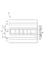
図3は、第1電極22Aと第2電極22Bとの間に加える電圧を説明する図である。第1電極22A及び第2電極22Bは、これに限定されるわけではないが、本実施形態では長方形である。そして、第1電極22Aの長手方向の両端には、銀ペースト等により導電部221A,222Aが設けられている。第2電極22Bの長手方向の両端には、銀ペースト等により導電部221B,222Bが設けられている。これらの導電部221A,222A,221B,222Bは、第1電極22A,第2電極22Bの長手方向の端部において短手方向に延びている。
[Voltage application]
FIG. 3 is a diagram illustrating a voltage applied between the
第1電極22Aの一端の導電部221Aには、電源20が取り付けられた給電部20Aが設けられ、給電部20Aより導電部221Aに所定の電圧E0が加えられる。この電圧E0の大きさは電源20を調整することにより可変である。なお、本実施形態では電圧は直流とするが、これに限定されず、交流であってもよい。
The
第2電極22Bの一端の導電部221Bは、接地されている。第1電極22Aの他端の導電部222Aには、三路スイッチ30が接続されている。三路スイッチ30により選択される一方の接点P1には、可変抵抗31の一端が接続され、可変抵抗31の他端は第2電極22Bの他端の導電部222Bに接続されている。三路スイッチ30により選択される他方の接点P2は、抵抗を介さずに、第2電極22Bの他端の導電部222Bに接続されている。
なお、本実施形態では、このように第1電極22Aの他端の導電部222Aが、三路スイッチ30により、可変抵抗31を介して第2電極22Bの他端の導電部222Bに接続されている側と、可変抵抗31を介さずに第2電極22Bの他端の導電部222Bに接続されている側と、のいずれかに選択的に接続される形態について説明した。しかし本発明はこれに限定されない。
第1電極22Aの他端の導電部222Aと第2電極22Bの他端の導電部222Bとは、三路スイッチ30を介さずに、例えば直接接触していてもよく、導電ペーストで貼り合わされていてもよく、導電線で接続、抵抗を介して接続または可変抵抗を介して接続されていてもよい。
The
In the present embodiment, the
The
第1電極22Aの導電部221Aに電圧E0が加えられ、第2電極22Bの導電部221Bがアースに接続されている場合の第1電極22A及び第2電極22Bの電位の状態を図4に示す。
FIG. 4 shows the potential states of the
三路スイッチ30が、接点P1及びP2のいずれとも接続されておらず、開いているときは、抵抗が無限大になるので、図4において点線で示すように、第1電極22Aは、電位E0で略一定であり、第2電極22Bは電位0である。
三路スイッチ30が、図3における接点P2に接続されている場合、抵抗値Rが略ゼロであるので、RI=0となり、図4において一点鎖線で示すような形になる。
三路スイッチ30が、図3における接点P1に接続されている場合、RIは可変抵抗31の抵抗値Rにより変化する。この可変抵抗31の抵抗値Rは、例えば、つまみ等で調整可能である。可変抵抗31の抵抗値Rが大きくなると、第1電極22Aの導電部222Aと、第2電極22Bの導電部222Bとの間の電位差RIが大きくなる。可変抵抗の抵抗値Rが小さくなると、第1電極22Aの導電部222Aと、第2電極22Bの導電部222Bとの間の電位差RIが小さくなる。
When the three-
When the three-
When the three-
図示するように、第1電極22Aの電位E1(x)は、一端側の導電部221Aにおいて、給電されたE0であるが、他端側の導電部222Aの方向に進むに従い下がる。
そして、導電部222Aの位置(一端側から距離Lの位置)において、電位はRI下がる(R:可変抵抗の抵抗値、I:可変抵抗を流れる電流)。
第2電極22Bの他端側の導電部222Bの電位E2(x)は、そのRI下がった電位であり、そこから一端側の導電部221Bに向かう従い下がり、導電部221Bにおいて、電位0Vとなる。
As shown in the drawing, the potential E 1 (x) of the
Then, at the position of the
The potential E 2 (x) of the
第1電極22A及び第2電極22Bの一端からの距離xの位置における、第1電極22Aの電位E1(x)と第2電極22Bの電位E2(x)との間の電位差(電圧)E(x)は以下のように表される。
E(x)=E1(x)−E2(x)・・・・・(1)
ここで、第1電極22Aの全長の抵抗値をR1、第2電極22Bの全長の抵抗値をR2とすると、
E1(x)=E0−R1Ix/L・・・・・(2)
E2=R2Ix/L・・・・・・・・・・・(3)
E0=I(R+R1+R2)・・・・・・・・・(4)
であるので、
(1)を(2)〜(4)を代入等して変形すると、
E(x)=E0−E0{(R1+R2)/(R+R1+R2)}x/L
となる。
At the position of distance x from one end of the
E (x) = E 1 (x) −E 2 (x) (1)
Here, if the resistance value of the entire length of the
E 1 (x) = E 0 −R 1 Ix / L (2)
E 2 = R 2 Ix / L (3)
E 0 = I (R + R 1 + R 2 ) (4)
So
If (1) is transformed by substituting (2) to (4), etc.,
E (x) = E 0 −E 0 {(R 1 + R 2 ) / (R + R 1 + R 2 )} x / L
It becomes.
ここで、図5は、調光フィルム10の透過率Tと、電位差E(x)との関係を示したグラフである。液晶の傾きは、電位差E(x)によって変化するので、調光フィルム10の透過率Tは、図示するように電位差E(x)の変化に応じて変化する。
Here, FIG. 5 is a graph showing the relationship between the transmittance T of the
本実施形態において、スイッチ30を接点P1に接続すると、調光フィルム10における第1電極22Aと第2電極22Bとの間の電位差E(x)は、長手方向の位置xによって、式(1)’のように変化する。したがって、調光フィルム10の透過率Tを、長手方向に漸次変化させる(グラデーションを付ける,濃淡を付ける)ことができる。また、その変化の割合を、抵抗値Rを変えることにより変更し、グラデーションを所望の濃淡にすることができる。
In the present embodiment, when the
また、図5に示すように、調光フィルム10の透過率Tと電位差Eとの関係はリニアではなく、電位差E(x)が0からV0までの間、透過率は0であり、V0を超えると急激に立ち上がり、V1を超えると徐々に傾きが緩やかになり、略一定となる。
すなわち、V0とV1との間において、透過率Tの変動が大きいので、図4に示す電位差E(x)が、このV0からV1の範囲で変化するようにすることで、透過率Tをより大きく変動させることができる。すなわち、グラデーションの幅を大きくすることができ、換言すると、濃淡の幅を大きくすることができる。
Further, as shown in FIG. 5, the relationship between the transmittance T and the potential difference E of the
That is, since the variation of the transmittance T is large between V 0 and V 1 , the potential difference E (x) shown in FIG. 4 is changed in the range of V 0 to V 1 , thereby transmitting the light. The rate T can be varied more greatly. That is, the gradation width can be increased, in other words, the shade width can be increased.
すなわち、
V0≦E(x)≦V1
であり、また、E(x)は、E0−E0(R1+R2)/(R+R1+R2)=IRとE0との間で変化するので、
IR≦V0<V1≦E0
である。
That is,
V 0 ≦ E (x) ≦ V 1
And E (x) varies between E 0 -E 0 (R 1 + R 2 ) / (R + R 1 + R 2 ) = IR and E 0 ,
IR ≦ V 0 <V 1 ≦ E 0
It is.
これを変形すると、
R≦V0/I=V0(R+R1+R2)/E0
E0R≦V0(R+R1+R2)
(E0−V0)R≦V0(R1+R2)
R≦V0(R1+R2)/(E0−V0)
従って、
0≦R≦V0(R1+R2)/(E0−V0)
If this is transformed,
R ≦ V 0 / I = V 0 (R + R 1 + R 2 ) / E 0
E 0 R ≦ V 0 (R + R 1 + R 2 )
(E 0 −V 0 ) R ≦ V 0 (R 1 + R 2 )
R ≦ V 0 (R 1 + R 2 ) / (E 0 −V 0 )
Therefore,
0 ≦ R ≦ V 0 (R 1 + R 2 ) / (E 0 −V 0 )
本実施形態によると、抵抗値Rをこの範囲にすることで、電圧の変化に対する透過率Tの変化量を大きくすることができ、調光フィルム10における、面内のグラデーションの濃淡の幅を大きくすることができる。但し、抵抗値Rの範囲は上式に限定されるものではない。
According to the present embodiment, by setting the resistance value R within this range, the amount of change in the transmittance T with respect to the change in voltage can be increased, and the gradation width of the in-plane gradation in the
(変形形態)
(1)以上、本発明の実施形態として、VA方式の液晶調光フィルムについて説明したが、本発明はこれに限定されず、電位差により調光量を調整できる他の方式であってもよい。
例えば、VA方式以外の液晶調光フィルムとして、TN方式(twisted Nematic liquid crystal)を用いてもよい。TN方式は、調光フィルムは、電圧がOFFのときは液晶分子が水平に並び、光を通過させて画面が「白」になる。徐々に電圧をかけていくと、液晶分子が垂直に立ち上がっていき、光をさえぎって画面が黒くなる方式である。
(Deformation)
(1) Although the VA liquid crystal light control film has been described as an embodiment of the present invention, the present invention is not limited to this, and may be another system capable of adjusting the light control amount by a potential difference.
For example, a TN method (twisted nematic liquid crystal) may be used as a liquid crystal light control film other than the VA method. In the TN system, when the voltage is OFF, the liquid crystal molecules are aligned horizontally in the TN system, and the light is allowed to pass through and the screen becomes “white”. When voltage is gradually applied, the liquid crystal molecules rise vertically, blocking the light and blacking the screen.
また、液晶以外を用いたものとして、例えば、EC方式、SPD方式、PDLC方式調光フィルムであってもよい。
EC方式(Electro chromic)を用いた調光フィルムは、一対の電極で調光層(電解質層)を挟んだ構造を有する。電極間の電位差に応じ、酸化還元反応を利用して調光層の色が透明と濃紺との間で変化する。
SPD方式(Suspended Particle Device)を用いた調光フィルムは、微粒子の配向を利用し、通常濃紺色に着色しているが、電圧をかけると透明に変化し、電圧を切ると元の濃紺色に戻るものであり、電圧によって濃淡を調整できる。
PDLC方式(Particle Dispersed Liquid Crystal)を用いた調光フィルムは、液晶層中に特殊なポリマーによるネットワーク構造体を形成させたもので、ポリマーネットワークの作用により、液晶分子の配列が不規則な状態を誘起して光を散乱させる。そして、電圧を印加することで、液晶分子を電界方向に配列させると、光が散乱されず、透明な状態となる。
調光フィルム
Moreover, as what uses liquid crystal other than a liquid crystal, for example, EC system, SPD system, and PDLC system light control film may be used.
A light control film using an EC system (Electrochromic) has a structure in which a light control layer (electrolyte layer) is sandwiched between a pair of electrodes. Depending on the potential difference between the electrodes, the color of the light control layer changes between transparent and dark blue using an oxidation-reduction reaction.
The light control film using the SPD method (Suspended Particle Device) is normally colored in dark blue using the orientation of fine particles, but it changes to transparent when a voltage is applied, and changes to the original dark blue when the voltage is turned off. It is a return, and the shade can be adjusted by the voltage.
The light control film using the PDLC method (Particle Dispersed Liquid Crystal) is a liquid crystal layer in which a network structure of a special polymer is formed. Due to the action of the polymer network, the arrangement of liquid crystal molecules is irregular. Induces and scatters light. When a voltage is applied to align the liquid crystal molecules in the electric field direction, the light is not scattered and becomes transparent.
Light control film
(2)本実施形態では、電圧を加えていない場合に透過率が低いノーマリーブラックについて説明したが、液晶の種類によっては、ノーマリーホワイトであってもよい。なお、上述のように、ノーマリーブラックとは、液晶に電圧がかかっていない時に透過率が最小となり、黒い画面になる構造である。ノーマリーホワイトとは、液晶に電圧がかかっていない時に透過率が最大となり、透明となる構造である。 (2) In this embodiment, a description has been given of normally black having low transmittance when no voltage is applied. However, normally white may be used depending on the type of liquid crystal. As described above, normally black is a structure in which the transmittance is minimized and a black screen is obtained when no voltage is applied to the liquid crystal. Normally white is a structure in which the transmittance is maximized and transparent when no voltage is applied to the liquid crystal.
(3)本実施形態では、矩形の電極の一辺から給電を行い、対向する他辺に三極スイッチを介して抵抗を接続したが、これに限定されない。例えば、給電は一辺の全体ではなく、一点から行っても良い。この場合、電位線は年輪状になる。
(4)また、矩形の電極の一辺から給電を行い、抵抗を接続する他辺は、対向する辺ではなく、隣接する辺であってもよい。さらには、給電を行う辺や、抵抗を接続する辺は、一辺ではなく二以上の辺であってもよい。
(5)本発明では、電極間に加える電流を直流としたが、これに限定されず交流でもよい。
(3) In the present embodiment, power is supplied from one side of the rectangular electrode, and a resistor is connected to the opposite side via a three-pole switch. However, the present invention is not limited to this. For example, the power supply may be performed from one point instead of the entire side. In this case, the potential line has an annual ring shape.
(4) Further, the other side to which power is supplied from one side of the rectangular electrode and the resistor is connected may be an adjacent side instead of an opposite side. Furthermore, the side to which power is fed and the side to which the resistor is connected may be two or more sides instead of one side.
(5) In the present invention, the current applied between the electrodes is a direct current. However, the present invention is not limited to this and may be an alternating current.
なお、図3の第2導電部222Bをアースすると、第1電極22Aの電位勾配は存在するが、第2電極22Bの電位勾配はなくなり一定の電圧(アース)となる。このような繋ぎ方をした場合に、斜め方向から見たときにグラデーションは付かないという現象が発生する。ただし、この場合であっても、正面方向から見た場合、面内でグラデーションを付けることがきる。
When the second
また、上述の実施形態では液晶セルを直線偏光板挟持して調光フィルムを構成する場合ついて述べたが、本発明はこれに限らず、ゲストホスト型液晶による液晶層を使用して直線偏光板を省略して調光フィルムを構成する場合にも広く適用することができる。 Further, in the above-described embodiment, the case where the liquid crystal cell is sandwiched between the linear polarizing plates to form the light control film is described. However, the present invention is not limited to this, and the linear polarizing plate using the liquid crystal layer of the guest-host type liquid crystal is used. The present invention can also be widely applied to the case where the light control film is constituted by omitting.
以上、本発明の実施に好適な具体的な構成を詳述したが、本発明は、本発明の趣旨を逸脱しない範囲で、上述の実施形態を種々に変更することができる。 As mentioned above, although the specific structure suitable for implementation of this invention was explained in full detail, this invention can be variously changed in the range which does not deviate from the meaning of this invention.
10 調光フィルム
12 第1の積層体
13 第2の積層体
14 液晶層
15 液晶セル
16,17 直線偏光板
18,19 位相差フィルム
20 電源
21A,21B 基材
22A 第1電極
22B 第2電極
23A,23B 配向層
24 スペーサー
25 シール材
30 三路スイッチ
31 可変抵抗
221A,221B,222A,222B 導電部
DESCRIPTION OF
Claims (4)
前記第1の電極に設けられるとともに、前記第1の電極と前記第2の電極との間に電圧を加える給電部と、
前記第1の電極と前記第2の電極との間に配置され、前記第1の電極と前記第2の電極との間に加えられた前記電圧によって透過率を変化させる調光材料と、を備え、
前記給電部と異なる位置において、前記第1の電極と前記第2の電極とが電気的に接続され、
前記第1の電極と前記第2の電極との間には抵抗部材が配置され、
前記抵抗部材の抵抗値が可変である、調光フィルム。 A first electrode and a second electrode arranged opposite to each other;
A power feeding unit that is provided on the first electrode and applies a voltage between the first electrode and the second electrode;
A light-modulating material that is disposed between the first electrode and the second electrode, and that changes transmittance by the voltage applied between the first electrode and the second electrode; Prepared,
The first electrode and the second electrode are electrically connected at a position different from the power feeding unit ,
A resistance member is disposed between the first electrode and the second electrode,
The light control film whose resistance value of the said resistance member is variable .
前記第1の電極に設けられるとともに、前記第1の電極と前記第2の電極との間に電圧を加える給電部と、
前記第1の電極と前記第2の電極との間に配置され、前記第1の電極と前記第2の電極との間に加えられた前記電圧によって透過率を変化させる調光材料と、を備え、
前記給電部と異なる位置において、前記第1の電極と前記第2の電極とが電気的に接続され、
前記第1の電極の一端側に前記給電部が設けられ、前記第1の電極の他端側と、前記第2の電極の他端側とが電気的に接続されている、調光フィルム。 A first electrode and a second electrode arranged opposite to each other;
A power feeding unit that is provided on the first electrode and applies a voltage between the first electrode and the second electrode;
A light-modulating material that is disposed between the first electrode and the second electrode, and that changes transmittance by the voltage applied between the first electrode and the second electrode; Prepared,
The first electrode and the second electrode are electrically connected at a position different from the power feeding unit ,
The light control film which the said electric power feeding part is provided in the one end side of the said 1st electrode, and the other end side of the said 1st electrode and the other end side of the said 2nd electrode are electrically connected .
前記第1の電極に設けられるとともに、前記第1の電極と前記第2の電極との間に電圧を加える給電部と、
前記第1の電極と前記第2の電極との間に配置され、前記第1の電極と前記第2の電極との間に加えられた前記電圧によって透過率を変化させる調光材料と、を備え、
前記給電部と異なる位置において、前記第1の電極と前記第2の電極とが電気的に接続され、
前記給電部は、複数個所に設けられている、調光フィルム。 A first electrode and a second electrode arranged opposite to each other;
A power feeding unit that is provided on the first electrode and applies a voltage between the first electrode and the second electrode;
A light-modulating material that is disposed between the first electrode and the second electrode, and that changes transmittance by the voltage applied between the first electrode and the second electrode; Prepared,
The first electrode and the second electrode are electrically connected at a position different from the power feeding unit ,
The said electric power feeding part is a light control film provided in several places .
前記第1の電極に設けられるとともに、前記第1の電極と前記第2の電極との間に電圧を加える給電部と、
前記第1の電極と前記第2の電極との間に配置され、前記第1の電極と前記第2の電極との間に加えられた前記電圧によって透過率を変化させる調光材料と、を備え、
前記給電部と異なる位置において、前記第1の電極と前記第2の電極とが電気的に接続され、
前記第1の電極と前記第2の電極とは、前記給電部と異なる複数個所において電気的に接続されている、調光フィルム。
A first electrode and a second electrode arranged opposite to each other;
A power feeding unit that is provided on the first electrode and applies a voltage between the first electrode and the second electrode;
A light-modulating material that is disposed between the first electrode and the second electrode, and that changes transmittance by the voltage applied between the first electrode and the second electrode; Prepared,
The first electrode and the second electrode are electrically connected at a position different from the power feeding unit ,
The light control film in which the first electrode and the second electrode are electrically connected at a plurality of locations different from the power feeding unit .
Priority Applications (8)
| Application Number | Priority Date | Filing Date | Title |
|---|---|---|---|
| JP2016121793A JP6128269B1 (en) | 2016-06-20 | 2016-06-20 | Light control film |
| KR1020187033706A KR102421609B1 (en) | 2016-06-20 | 2017-06-16 | Light control film, driving method of light control film, light control member, vehicle |
| EP17815306.0A EP3474066B1 (en) | 2016-06-20 | 2017-06-16 | Light control film, method for driving light control film, light control member, and vehicle |
| PCT/JP2017/022366 WO2017221838A1 (en) | 2016-06-20 | 2017-06-16 | Light control film, method for driving light control film, light control member, and vehicle |
| US16/310,214 US10845522B2 (en) | 2016-06-20 | 2017-06-16 | Light control film, method for driving light control film, light control member, and vehicle |
| CN201780033490.7A CN109219770B (en) | 2016-06-20 | 2017-06-16 | Light adjusting film, driving method of light adjusting film, light adjusting member, and vehicle |
| US17/088,648 US11520095B2 (en) | 2016-06-20 | 2020-11-04 | Light control film, method for driving light control film, light control member, and vehicle |
| US17/977,419 US11835745B2 (en) | 2016-06-20 | 2022-10-31 | Light control film, method for driving light control film, light control member, and vehicle |
Applications Claiming Priority (1)
| Application Number | Priority Date | Filing Date | Title |
|---|---|---|---|
| JP2016121793A JP6128269B1 (en) | 2016-06-20 | 2016-06-20 | Light control film |
Publications (2)
| Publication Number | Publication Date |
|---|---|
| JP6128269B1 true JP6128269B1 (en) | 2017-05-17 |
| JP2017227675A JP2017227675A (en) | 2017-12-28 |
Family
ID=58714735
Family Applications (1)
| Application Number | Title | Priority Date | Filing Date |
|---|---|---|---|
| JP2016121793A Active JP6128269B1 (en) | 2016-06-20 | 2016-06-20 | Light control film |
Country Status (1)
| Country | Link |
|---|---|
| JP (1) | JP6128269B1 (en) |
Cited By (3)
| Publication number | Priority date | Publication date | Assignee | Title |
|---|---|---|---|---|
| CN107799016A (en) * | 2017-11-07 | 2018-03-13 | 南磊 | A kind of seamless display method of the additional black and white transflective liquid crystal screen of LED color screens |
| JP2019064376A (en) * | 2017-09-29 | 2019-04-25 | 大日本印刷株式会社 | Peeping prevention system for movable body |
| US11016355B2 (en) | 2018-01-30 | 2021-05-25 | Dai Nippon Printing Co., Ltd. | Liquid crystal light control apparatus and method for manufacturing same |
Families Citing this family (1)
| Publication number | Priority date | Publication date | Assignee | Title |
|---|---|---|---|---|
| JP7169528B2 (en) * | 2018-01-30 | 2022-11-11 | 大日本印刷株式会社 | Liquid crystal light control device and its driving method |
Citations (5)
| Publication number | Priority date | Publication date | Assignee | Title |
|---|---|---|---|---|
| JPS5962830A (en) * | 1983-07-11 | 1984-04-10 | Canon Inc | Liquid crystal display device |
| JPS6338921A (en) * | 1986-08-04 | 1988-02-19 | Nippon Telegr & Teleph Corp <Ntt> | Driving method for liquid crystal cell |
| JPH01186911A (en) * | 1988-01-21 | 1989-07-26 | Asahi Glass Co Ltd | Dimming device and its manufacture |
| JPH0299919A (en) * | 1988-10-06 | 1990-04-11 | Ajinomoto Co Inc | Optical modulating plate made of liquid crystal-containing resin |
| JPH05178645A (en) * | 1990-09-14 | 1993-07-20 | Saint Gobain Vitrage Internatl | Electrochromic windowpane |
-
2016
- 2016-06-20 JP JP2016121793A patent/JP6128269B1/en active Active
Patent Citations (5)
| Publication number | Priority date | Publication date | Assignee | Title |
|---|---|---|---|---|
| JPS5962830A (en) * | 1983-07-11 | 1984-04-10 | Canon Inc | Liquid crystal display device |
| JPS6338921A (en) * | 1986-08-04 | 1988-02-19 | Nippon Telegr & Teleph Corp <Ntt> | Driving method for liquid crystal cell |
| JPH01186911A (en) * | 1988-01-21 | 1989-07-26 | Asahi Glass Co Ltd | Dimming device and its manufacture |
| JPH0299919A (en) * | 1988-10-06 | 1990-04-11 | Ajinomoto Co Inc | Optical modulating plate made of liquid crystal-containing resin |
| JPH05178645A (en) * | 1990-09-14 | 1993-07-20 | Saint Gobain Vitrage Internatl | Electrochromic windowpane |
Cited By (3)
| Publication number | Priority date | Publication date | Assignee | Title |
|---|---|---|---|---|
| JP2019064376A (en) * | 2017-09-29 | 2019-04-25 | 大日本印刷株式会社 | Peeping prevention system for movable body |
| CN107799016A (en) * | 2017-11-07 | 2018-03-13 | 南磊 | A kind of seamless display method of the additional black and white transflective liquid crystal screen of LED color screens |
| US11016355B2 (en) | 2018-01-30 | 2021-05-25 | Dai Nippon Printing Co., Ltd. | Liquid crystal light control apparatus and method for manufacturing same |
Also Published As
| Publication number | Publication date |
|---|---|
| JP2017227675A (en) | 2017-12-28 |
Similar Documents
| Publication | Publication Date | Title |
|---|---|---|
| KR102421609B1 (en) | Light control film, driving method of light control film, light control member, vehicle | |
| JP6128270B1 (en) | Light control film | |
| JP2022043240A (en) | Photochromic system and method for driving photochromic film | |
| US8525955B2 (en) | Heater for liquid crystal display | |
| JP6128269B1 (en) | Light control film | |
| CN111983863A (en) | Dimming glass | |
| CN109477987B (en) | Light-adjusting film, light-adjusting member, vehicle, and power supply method for light-adjusting film | |
| JP2011095407A (en) | Display device | |
| TWI592724B (en) | Dimming film | |
| US12174493B2 (en) | Liquid crystal light control device | |
| JP5423603B2 (en) | Suspended particle device and driving method thereof | |
| TWI345653B (en) | Liquid crystal display device and display method of same | |
| JP2019070778A (en) | Dimming film, dimming member, vehicle, dimming system and method for driving dimming film | |
| JP2018025786A (en) | Lighting control film, lighting control member and power supply method for vehicle and lighting control film | |
| US20130271680A1 (en) | Liquid crystal panel, and liquid crystal display | |
| JP2018018074A (en) | Light control film, method for driving light control film, light control device, light control member and vehicle | |
| JP2018018073A (en) | Light control film, method for driving light control film, light control device, light control member and vehicle | |
| JP2018060128A (en) | Lighting control film and driving method of lighting control film | |
| JP2019101384A (en) | Dimming film and dimming member | |
| WO2020189715A1 (en) | Dimming sheet, dimming device, and method for managing dimming sheet | |
| JP6057012B1 (en) | Light control film | |
| JP7074071B2 (en) | Dimming film | |
| JP2018112629A (en) | Light control cell | |
| JP2018106079A (en) | Dimming film | |
| JP2024069407A (en) | Dimming member |
Legal Events
| Date | Code | Title | Description |
|---|---|---|---|
| A621 | Written request for application examination |
Free format text: JAPANESE INTERMEDIATE CODE: A621 Effective date: 20160801 |
|
| A871 | Explanation of circumstances concerning accelerated examination |
Free format text: JAPANESE INTERMEDIATE CODE: A871 Effective date: 20160801 |
|
| RD04 | Notification of resignation of power of attorney |
Free format text: JAPANESE INTERMEDIATE CODE: A7424 Effective date: 20160928 |
|
| A975 | Report on accelerated examination |
Free format text: JAPANESE INTERMEDIATE CODE: A971005 Effective date: 20161122 |
|
| A977 | Report on retrieval |
Free format text: JAPANESE INTERMEDIATE CODE: A971007 Effective date: 20161124 |
|
| A131 | Notification of reasons for refusal |
Free format text: JAPANESE INTERMEDIATE CODE: A131 Effective date: 20161206 |
|
| A521 | Written amendment |
Free format text: JAPANESE INTERMEDIATE CODE: A523 Effective date: 20170119 |
|
| TRDD | Decision of grant or rejection written | ||
| A01 | Written decision to grant a patent or to grant a registration (utility model) |
Free format text: JAPANESE INTERMEDIATE CODE: A01 Effective date: 20170314 |
|
| A61 | First payment of annual fees (during grant procedure) |
Free format text: JAPANESE INTERMEDIATE CODE: A61 Effective date: 20170327 |
|
| R150 | Certificate of patent or registration of utility model |
Ref document number: 6128269 Country of ref document: JP Free format text: JAPANESE INTERMEDIATE CODE: R150 |