JP6079502B2 - Solid-state imaging device and electronic device - Google Patents
Solid-state imaging device and electronic device Download PDFInfo
- Publication number
- JP6079502B2 JP6079502B2 JP2013169553A JP2013169553A JP6079502B2 JP 6079502 B2 JP6079502 B2 JP 6079502B2 JP 2013169553 A JP2013169553 A JP 2013169553A JP 2013169553 A JP2013169553 A JP 2013169553A JP 6079502 B2 JP6079502 B2 JP 6079502B2
- Authority
- JP
- Japan
- Prior art keywords
- semiconductor substrate
- solid
- electrode
- separation groove
- state imaging
- Prior art date
- Legal status (The legal status is an assumption and is not a legal conclusion. Google has not performed a legal analysis and makes no representation as to the accuracy of the status listed.)
- Active
Links
- 238000003384 imaging method Methods 0.000 title claims description 125
- 239000000758 substrate Substances 0.000 claims description 211
- 239000004065 semiconductor Substances 0.000 claims description 204
- 238000006243 chemical reaction Methods 0.000 claims description 115
- 238000000926 separation method Methods 0.000 claims description 105
- 238000009792 diffusion process Methods 0.000 claims description 48
- 239000012535 impurity Substances 0.000 claims description 20
- 229910052751 metal Inorganic materials 0.000 claims description 10
- 239000004020 conductor Substances 0.000 claims description 9
- 239000002184 metal Substances 0.000 claims description 9
- 238000002955 isolation Methods 0.000 claims description 6
- 239000010410 layer Substances 0.000 description 94
- 238000000034 method Methods 0.000 description 46
- 238000009825 accumulation Methods 0.000 description 13
- 238000010586 diagram Methods 0.000 description 12
- XUIMIQQOPSSXEZ-UHFFFAOYSA-N Silicon Chemical compound [Si] XUIMIQQOPSSXEZ-UHFFFAOYSA-N 0.000 description 11
- 230000004048 modification Effects 0.000 description 11
- 238000012986 modification Methods 0.000 description 11
- 229910052710 silicon Inorganic materials 0.000 description 11
- 239000010703 silicon Substances 0.000 description 11
- 239000000463 material Substances 0.000 description 10
- 230000006870 function Effects 0.000 description 8
- 238000004519 manufacturing process Methods 0.000 description 7
- 239000007769 metal material Substances 0.000 description 7
- 230000003287 optical effect Effects 0.000 description 7
- 238000001312 dry etching Methods 0.000 description 6
- 230000000694 effects Effects 0.000 description 6
- 238000005468 ion implantation Methods 0.000 description 6
- 230000001681 protective effect Effects 0.000 description 6
- VYPSYNLAJGMNEJ-UHFFFAOYSA-N Silicium dioxide Chemical compound O=[Si]=O VYPSYNLAJGMNEJ-UHFFFAOYSA-N 0.000 description 5
- BOTDANWDWHJENH-UHFFFAOYSA-N Tetraethyl orthosilicate Chemical compound CCO[Si](OCC)(OCC)OCC BOTDANWDWHJENH-UHFFFAOYSA-N 0.000 description 5
- 229910052782 aluminium Inorganic materials 0.000 description 5
- XAGFODPZIPBFFR-UHFFFAOYSA-N aluminium Chemical compound [Al] XAGFODPZIPBFFR-UHFFFAOYSA-N 0.000 description 5
- 229910052735 hafnium Inorganic materials 0.000 description 5
- VBJZVLUMGGDVMO-UHFFFAOYSA-N hafnium atom Chemical compound [Hf] VBJZVLUMGGDVMO-UHFFFAOYSA-N 0.000 description 5
- 239000011229 interlayer Substances 0.000 description 5
- 229910052814 silicon oxide Inorganic materials 0.000 description 5
- 238000005229 chemical vapour deposition Methods 0.000 description 4
- MRELNEQAGSRDBK-UHFFFAOYSA-N lanthanum(3+);oxygen(2-) Chemical compound [O-2].[O-2].[O-2].[La+3].[La+3] MRELNEQAGSRDBK-UHFFFAOYSA-N 0.000 description 4
- PLDDOISOJJCEMH-UHFFFAOYSA-N neodymium(3+);oxygen(2-) Chemical compound [O-2].[O-2].[O-2].[Nd+3].[Nd+3] PLDDOISOJJCEMH-UHFFFAOYSA-N 0.000 description 4
- 230000000149 penetrating effect Effects 0.000 description 4
- ZIKATJAYWZUJPY-UHFFFAOYSA-N thulium(iii) oxide Chemical compound [O-2].[O-2].[O-2].[Tm+3].[Tm+3] ZIKATJAYWZUJPY-UHFFFAOYSA-N 0.000 description 4
- 229910052581 Si3N4 Inorganic materials 0.000 description 3
- RTAQQCXQSZGOHL-UHFFFAOYSA-N Titanium Chemical compound [Ti] RTAQQCXQSZGOHL-UHFFFAOYSA-N 0.000 description 3
- 238000000137 annealing Methods 0.000 description 3
- 229910017052 cobalt Inorganic materials 0.000 description 3
- 239000010941 cobalt Substances 0.000 description 3
- GUTLYIVDDKVIGB-UHFFFAOYSA-N cobalt atom Chemical compound [Co] GUTLYIVDDKVIGB-UHFFFAOYSA-N 0.000 description 3
- 239000012212 insulator Substances 0.000 description 3
- 230000002093 peripheral effect Effects 0.000 description 3
- HQVNEWCFYHHQES-UHFFFAOYSA-N silicon nitride Chemical compound N12[Si]34N5[Si]62N3[Si]51N64 HQVNEWCFYHHQES-UHFFFAOYSA-N 0.000 description 3
- 229910052715 tantalum Inorganic materials 0.000 description 3
- GUVRBAGPIYLISA-UHFFFAOYSA-N tantalum atom Chemical compound [Ta] GUVRBAGPIYLISA-UHFFFAOYSA-N 0.000 description 3
- 229910052719 titanium Inorganic materials 0.000 description 3
- 239000010936 titanium Substances 0.000 description 3
- WFKWXMTUELFFGS-UHFFFAOYSA-N tungsten Chemical compound [W] WFKWXMTUELFFGS-UHFFFAOYSA-N 0.000 description 3
- 229910052721 tungsten Inorganic materials 0.000 description 3
- 239000010937 tungsten Substances 0.000 description 3
- IJGRMHOSHXDMSA-UHFFFAOYSA-N Atomic nitrogen Chemical compound N#N IJGRMHOSHXDMSA-UHFFFAOYSA-N 0.000 description 2
- 241000519995 Stachys sylvatica Species 0.000 description 2
- GWEVSGVZZGPLCZ-UHFFFAOYSA-N Titan oxide Chemical compound O=[Ti]=O GWEVSGVZZGPLCZ-UHFFFAOYSA-N 0.000 description 2
- 206010047571 Visual impairment Diseases 0.000 description 2
- UPEMFLOMQVFMCZ-UHFFFAOYSA-N [O--].[O--].[O--].[Pm+3].[Pm+3] Chemical compound [O--].[O--].[O--].[Pm+3].[Pm+3] UPEMFLOMQVFMCZ-UHFFFAOYSA-N 0.000 description 2
- 230000015572 biosynthetic process Effects 0.000 description 2
- 229910000420 cerium oxide Inorganic materials 0.000 description 2
- 239000000470 constituent Substances 0.000 description 2
- PMHQVHHXPFUNSP-UHFFFAOYSA-M copper(1+);methylsulfanylmethane;bromide Chemical compound Br[Cu].CSC PMHQVHHXPFUNSP-UHFFFAOYSA-M 0.000 description 2
- 229910003440 dysprosium oxide Inorganic materials 0.000 description 2
- NLQFUUYNQFMIJW-UHFFFAOYSA-N dysprosium(iii) oxide Chemical compound O=[Dy]O[Dy]=O NLQFUUYNQFMIJW-UHFFFAOYSA-N 0.000 description 2
- 229910001940 europium oxide Inorganic materials 0.000 description 2
- 229940075616 europium oxide Drugs 0.000 description 2
- AEBZCFFCDTZXHP-UHFFFAOYSA-N europium(3+);oxygen(2-) Chemical compound [O-2].[O-2].[O-2].[Eu+3].[Eu+3] AEBZCFFCDTZXHP-UHFFFAOYSA-N 0.000 description 2
- 229910001938 gadolinium oxide Inorganic materials 0.000 description 2
- 229940075613 gadolinium oxide Drugs 0.000 description 2
- CMIHHWBVHJVIGI-UHFFFAOYSA-N gadolinium(iii) oxide Chemical compound [O-2].[O-2].[O-2].[Gd+3].[Gd+3] CMIHHWBVHJVIGI-UHFFFAOYSA-N 0.000 description 2
- 229910000449 hafnium oxide Inorganic materials 0.000 description 2
- WIHZLLGSGQNAGK-UHFFFAOYSA-N hafnium(4+);oxygen(2-) Chemical compound [O-2].[O-2].[Hf+4] WIHZLLGSGQNAGK-UHFFFAOYSA-N 0.000 description 2
- JYTUFVYWTIKZGR-UHFFFAOYSA-N holmium oxide Inorganic materials [O][Ho]O[Ho][O] JYTUFVYWTIKZGR-UHFFFAOYSA-N 0.000 description 2
- OWCYYNSBGXMRQN-UHFFFAOYSA-N holmium(3+);oxygen(2-) Chemical compound [O-2].[O-2].[O-2].[Ho+3].[Ho+3] OWCYYNSBGXMRQN-UHFFFAOYSA-N 0.000 description 2
- 229910003443 lutetium oxide Inorganic materials 0.000 description 2
- 230000001590 oxidative effect Effects 0.000 description 2
- TWNQGVIAIRXVLR-UHFFFAOYSA-N oxo(oxoalumanyloxy)alumane Chemical compound O=[Al]O[Al]=O TWNQGVIAIRXVLR-UHFFFAOYSA-N 0.000 description 2
- BMMGVYCKOGBVEV-UHFFFAOYSA-N oxo(oxoceriooxy)cerium Chemical compound [Ce]=O.O=[Ce]=O BMMGVYCKOGBVEV-UHFFFAOYSA-N 0.000 description 2
- MPARYNQUYZOBJM-UHFFFAOYSA-N oxo(oxolutetiooxy)lutetium Chemical compound O=[Lu]O[Lu]=O MPARYNQUYZOBJM-UHFFFAOYSA-N 0.000 description 2
- MMKQUGHLEMYQSG-UHFFFAOYSA-N oxygen(2-);praseodymium(3+) Chemical compound [O-2].[O-2].[O-2].[Pr+3].[Pr+3] MMKQUGHLEMYQSG-UHFFFAOYSA-N 0.000 description 2
- BPUBBGLMJRNUCC-UHFFFAOYSA-N oxygen(2-);tantalum(5+) Chemical compound [O-2].[O-2].[O-2].[O-2].[O-2].[Ta+5].[Ta+5] BPUBBGLMJRNUCC-UHFFFAOYSA-N 0.000 description 2
- UZLYXNNZYFBAQO-UHFFFAOYSA-N oxygen(2-);ytterbium(3+) Chemical compound [O-2].[O-2].[O-2].[Yb+3].[Yb+3] UZLYXNNZYFBAQO-UHFFFAOYSA-N 0.000 description 2
- RVTZCBVAJQQJTK-UHFFFAOYSA-N oxygen(2-);zirconium(4+) Chemical compound [O-2].[O-2].[Zr+4] RVTZCBVAJQQJTK-UHFFFAOYSA-N 0.000 description 2
- 229910003447 praseodymium oxide Inorganic materials 0.000 description 2
- 229910001954 samarium oxide Inorganic materials 0.000 description 2
- 229940075630 samarium oxide Drugs 0.000 description 2
- FKTOIHSPIPYAPE-UHFFFAOYSA-N samarium(iii) oxide Chemical compound [O-2].[O-2].[O-2].[Sm+3].[Sm+3] FKTOIHSPIPYAPE-UHFFFAOYSA-N 0.000 description 2
- 239000002210 silicon-based material Substances 0.000 description 2
- 229910001936 tantalum oxide Inorganic materials 0.000 description 2
- 229910003451 terbium oxide Inorganic materials 0.000 description 2
- SCRZPWWVSXWCMC-UHFFFAOYSA-N terbium(iii) oxide Chemical compound [O-2].[O-2].[O-2].[Tb+3].[Tb+3] SCRZPWWVSXWCMC-UHFFFAOYSA-N 0.000 description 2
- OGIDPMRJRNCKJF-UHFFFAOYSA-N titanium oxide Inorganic materials [Ti]=O OGIDPMRJRNCKJF-UHFFFAOYSA-N 0.000 description 2
- 229910003454 ytterbium oxide Inorganic materials 0.000 description 2
- 229940075624 ytterbium oxide Drugs 0.000 description 2
- 229910052727 yttrium Inorganic materials 0.000 description 2
- VWQVUPCCIRVNHF-UHFFFAOYSA-N yttrium atom Chemical compound [Y] VWQVUPCCIRVNHF-UHFFFAOYSA-N 0.000 description 2
- 229910001928 zirconium oxide Inorganic materials 0.000 description 2
- UFHFLCQGNIYNRP-UHFFFAOYSA-N Hydrogen Chemical compound [H][H] UFHFLCQGNIYNRP-UHFFFAOYSA-N 0.000 description 1
- OAICVXFJPJFONN-UHFFFAOYSA-N Phosphorus Chemical compound [P] OAICVXFJPJFONN-UHFFFAOYSA-N 0.000 description 1
- NRCMAYZCPIVABH-UHFFFAOYSA-N Quinacridone Chemical compound N1C2=CC=CC=C2C(=O)C2=C1C=C1C(=O)C3=CC=CC=C3NC1=C2 NRCMAYZCPIVABH-UHFFFAOYSA-N 0.000 description 1
- 102220469588 Voltage-dependent L-type calcium channel subunit beta-2_D60A_mutation Human genes 0.000 description 1
- 238000010521 absorption reaction Methods 0.000 description 1
- 229910021417 amorphous silicon Inorganic materials 0.000 description 1
- 230000005540 biological transmission Effects 0.000 description 1
- 230000000295 complement effect Effects 0.000 description 1
- 230000007547 defect Effects 0.000 description 1
- 239000000975 dye Substances 0.000 description 1
- 230000005684 electric field Effects 0.000 description 1
- 239000007789 gas Substances 0.000 description 1
- 239000001257 hydrogen Substances 0.000 description 1
- 229910052739 hydrogen Inorganic materials 0.000 description 1
- AMGQUBHHOARCQH-UHFFFAOYSA-N indium;oxotin Chemical compound [In].[Sn]=O AMGQUBHHOARCQH-UHFFFAOYSA-N 0.000 description 1
- 239000011159 matrix material Substances 0.000 description 1
- 229910044991 metal oxide Inorganic materials 0.000 description 1
- 150000004706 metal oxides Chemical class 0.000 description 1
- 229910052757 nitrogen Inorganic materials 0.000 description 1
- 230000035515 penetration Effects 0.000 description 1
- 229910052698 phosphorus Inorganic materials 0.000 description 1
- 239000011574 phosphorus Substances 0.000 description 1
- 238000005498 polishing Methods 0.000 description 1
- 230000004044 response Effects 0.000 description 1
- 210000001525 retina Anatomy 0.000 description 1
- 239000001022 rhodamine dye Substances 0.000 description 1
- LIVNPJMFVYWSIS-UHFFFAOYSA-N silicon monoxide Chemical compound [Si-]#[O+] LIVNPJMFVYWSIS-UHFFFAOYSA-N 0.000 description 1
- 239000007787 solid Substances 0.000 description 1
- 230000003595 spectral effect Effects 0.000 description 1
- 238000004611 spectroscopical analysis Methods 0.000 description 1
- 238000001228 spectrum Methods 0.000 description 1
- 238000003860 storage Methods 0.000 description 1
- 239000000126 substance Substances 0.000 description 1
Images


Classifications
-
- H—ELECTRICITY
- H10—SEMICONDUCTOR DEVICES; ELECTRIC SOLID-STATE DEVICES NOT OTHERWISE PROVIDED FOR
- H10F—INORGANIC SEMICONDUCTOR DEVICES SENSITIVE TO INFRARED RADIATION, LIGHT, ELECTROMAGNETIC RADIATION OF SHORTER WAVELENGTH OR CORPUSCULAR RADIATION
- H10F39/00—Integrated devices, or assemblies of multiple devices, comprising at least one element covered by group H10F30/00, e.g. radiation detectors comprising photodiode arrays
- H10F39/80—Constructional details of image sensors
- H10F39/811—Interconnections
-
- H—ELECTRICITY
- H01—ELECTRIC ELEMENTS
- H01L—SEMICONDUCTOR DEVICES NOT COVERED BY CLASS H10
- H01L21/00—Processes or apparatus adapted for the manufacture or treatment of semiconductor or solid state devices or of parts thereof
- H01L21/70—Manufacture or treatment of devices consisting of a plurality of solid state components formed in or on a common substrate or of parts thereof; Manufacture of integrated circuit devices or of parts thereof
- H01L21/71—Manufacture of specific parts of devices defined in group H01L21/70
- H01L21/768—Applying interconnections to be used for carrying current between separate components within a device comprising conductors and dielectrics
- H01L21/76898—Applying interconnections to be used for carrying current between separate components within a device comprising conductors and dielectrics formed through a semiconductor substrate
-
- H—ELECTRICITY
- H01—ELECTRIC ELEMENTS
- H01L—SEMICONDUCTOR DEVICES NOT COVERED BY CLASS H10
- H01L23/00—Details of semiconductor or other solid state devices
- H01L23/48—Arrangements for conducting electric current to or from the solid state body in operation, e.g. leads, terminal arrangements ; Selection of materials therefor
- H01L23/481—Internal lead connections, e.g. via connections, feedthrough structures
-
- H—ELECTRICITY
- H04—ELECTRIC COMMUNICATION TECHNIQUE
- H04N—PICTORIAL COMMUNICATION, e.g. TELEVISION
- H04N25/00—Circuitry of solid-state image sensors [SSIS]; Control thereof
- H04N25/70—SSIS architectures; Circuits associated therewith
- H04N25/76—Addressed sensors, e.g. MOS or CMOS sensors
- H04N25/77—Pixel circuitry, e.g. memories, A/D converters, pixel amplifiers, shared circuits or shared components
-
- H—ELECTRICITY
- H04—ELECTRIC COMMUNICATION TECHNIQUE
- H04N—PICTORIAL COMMUNICATION, e.g. TELEVISION
- H04N25/00—Circuitry of solid-state image sensors [SSIS]; Control thereof
- H04N25/70—SSIS architectures; Circuits associated therewith
- H04N25/76—Addressed sensors, e.g. MOS or CMOS sensors
- H04N25/78—Readout circuits for addressed sensors, e.g. output amplifiers or A/D converters
-
- H—ELECTRICITY
- H04—ELECTRIC COMMUNICATION TECHNIQUE
- H04N—PICTORIAL COMMUNICATION, e.g. TELEVISION
- H04N25/00—Circuitry of solid-state image sensors [SSIS]; Control thereof
- H04N25/70—SSIS architectures; Circuits associated therewith
- H04N25/79—Arrangements of circuitry being divided between different or multiple substrates, chips or circuit boards, e.g. stacked image sensors
-
- H—ELECTRICITY
- H10—SEMICONDUCTOR DEVICES; ELECTRIC SOLID-STATE DEVICES NOT OTHERWISE PROVIDED FOR
- H10F—INORGANIC SEMICONDUCTOR DEVICES SENSITIVE TO INFRARED RADIATION, LIGHT, ELECTROMAGNETIC RADIATION OF SHORTER WAVELENGTH OR CORPUSCULAR RADIATION
- H10F39/00—Integrated devices, or assemblies of multiple devices, comprising at least one element covered by group H10F30/00, e.g. radiation detectors comprising photodiode arrays
- H10F39/10—Integrated devices
- H10F39/12—Image sensors
- H10F39/18—Complementary metal-oxide-semiconductor [CMOS] image sensors; Photodiode array image sensors
- H10F39/182—Colour image sensors
- H10F39/1825—Multicolour image sensors having stacked structure, e.g. NPN, NPNPN or multiple quantum well [MQW] structures
-
- H—ELECTRICITY
- H10—SEMICONDUCTOR DEVICES; ELECTRIC SOLID-STATE DEVICES NOT OTHERWISE PROVIDED FOR
- H10F—INORGANIC SEMICONDUCTOR DEVICES SENSITIVE TO INFRARED RADIATION, LIGHT, ELECTROMAGNETIC RADIATION OF SHORTER WAVELENGTH OR CORPUSCULAR RADIATION
- H10F39/00—Integrated devices, or assemblies of multiple devices, comprising at least one element covered by group H10F30/00, e.g. radiation detectors comprising photodiode arrays
- H10F39/10—Integrated devices
- H10F39/12—Image sensors
- H10F39/199—Back-illuminated image sensors
-
- H—ELECTRICITY
- H01—ELECTRIC ELEMENTS
- H01L—SEMICONDUCTOR DEVICES NOT COVERED BY CLASS H10
- H01L21/00—Processes or apparatus adapted for the manufacture or treatment of semiconductor or solid state devices or of parts thereof
- H01L21/70—Manufacture or treatment of devices consisting of a plurality of solid state components formed in or on a common substrate or of parts thereof; Manufacture of integrated circuit devices or of parts thereof
- H01L21/71—Manufacture of specific parts of devices defined in group H01L21/70
- H01L21/768—Applying interconnections to be used for carrying current between separate components within a device comprising conductors and dielectrics
- H01L21/76801—Applying interconnections to be used for carrying current between separate components within a device comprising conductors and dielectrics characterised by the formation and the after-treatment of the dielectrics, e.g. smoothing
- H01L21/7682—Applying interconnections to be used for carrying current between separate components within a device comprising conductors and dielectrics characterised by the formation and the after-treatment of the dielectrics, e.g. smoothing the dielectric comprising air gaps
-
- H—ELECTRICITY
- H01—ELECTRIC ELEMENTS
- H01L—SEMICONDUCTOR DEVICES NOT COVERED BY CLASS H10
- H01L2924/00—Indexing scheme for arrangements or methods for connecting or disconnecting semiconductor or solid-state bodies as covered by H01L24/00
- H01L2924/0001—Technical content checked by a classifier
- H01L2924/0002—Not covered by any one of groups H01L24/00, H01L24/00 and H01L2224/00
Landscapes
- Engineering & Computer Science (AREA)
- Multimedia (AREA)
- Signal Processing (AREA)
- Physics & Mathematics (AREA)
- Condensed Matter Physics & Semiconductors (AREA)
- General Physics & Mathematics (AREA)
- Computer Hardware Design (AREA)
- Microelectronics & Electronic Packaging (AREA)
- Power Engineering (AREA)
- Manufacturing & Machinery (AREA)
- Solid State Image Pick-Up Elements (AREA)
- Transforming Light Signals Into Electric Signals (AREA)
Description
本開示は、いわゆる縦方向分光型に好適な固体撮像素子およびこの固体撮像素子を備えた電子機器に関する。 The present disclosure relates to a solid-state imaging device suitable for a so-called vertical spectroscopic type and an electronic apparatus including the solid-state imaging device.
デジタルビデオカメラ、デジタルスチルカメラ、携帯電話やスマートフォン等に搭載される固体撮像装置として、例えばCMOS(Complementary Metal Oxide Semiconductor )イメージセンサが挙げられる。CMOSイメージセンサでは、光電変換素子であるフォトダイオードのpn接合容量に蓄積した光電荷が、MOSトランジスタを介して読み出される。 As a solid-state imaging device mounted on a digital video camera, a digital still camera, a mobile phone, a smartphone, or the like, for example, a CMOS (Complementary Metal Oxide Semiconductor) image sensor can be given. In a CMOS image sensor, photocharge accumulated in a pn junction capacitance of a photodiode that is a photoelectric conversion element is read out through a MOS transistor.
既存の固体撮像装置では、赤、緑および青の画素を平面上に並べた画素配列が広く用いられているが、この構成では、画素間の補間処理を行って色信号を生成することに伴い、偽色が発生する。そのため、同一画素の縦方向に赤、緑および青の光電変換領域を積層した縦方向分光型の固体撮像素子が検討されている。例えば特許文献1には、半導体基板内に青および赤のフォトダイオードを積層し、半導体基板の受光面側(裏面側、第1面側)に有機光電変換膜を用いた緑の光電変換素子を設けた固体撮像素子が記載されている。
In an existing solid-state imaging device, a pixel array in which red, green, and blue pixels are arranged on a plane is widely used. With this configuration, interpolating between pixels is performed to generate a color signal. , False color occurs. Therefore, a vertical-spectral-type solid-state imaging device in which red, green, and blue photoelectric conversion regions are stacked in the vertical direction of the same pixel has been studied. For example,
特許文献1では、緑の光電変換素子で生じた電荷は、半導体基板を貫通する導電性プラグを通じて半導体基板の配線層側(表面側、第2面側)のn型半導体領域に蓄積されると説明されている。導電性プラグは、半導体基板の第1面側の光電変換素子からの電荷を半導体基板の第2面側に良好に転送し、変換効率などの特性を高めるために重要であるが、導電性プラグの構成については未だ検討の余地が残されていた。
In
本開示はかかる問題点に鑑みてなされたもので、その目的は、特性を高めることが可能な固体撮像素子およびこの固体撮像素子を備えた電子機器を提供することにある。 The present disclosure has been made in view of such problems, and an object of the present disclosure is to provide a solid-state imaging device capable of improving characteristics and an electronic apparatus including the solid-state imaging device.
本開示に係る第1の固体撮像素子は、半導体基板の第1面側に設けられた光電変換素子と、光電変換素子に接続され、半導体基板の第1面と第2面との間に設けられた貫通電極と、分離溝を充填し、絶縁性を有する誘電体層と、貫通電極と半導体基板との間に設けられた分離溝と、分離溝の外側面、内側面および底面と、半導体基板の第1面とに設けられた固定電荷を有する膜とを備えたものである。
A first solid-state imaging device according to the present disclosure is provided between a photoelectric conversion element provided on a first surface side of a semiconductor substrate and a first surface and a second surface of the semiconductor substrate connected to the photoelectric conversion element. Penetrating electrode formed, dielectric layer filling insulating groove, insulating layer, separating groove provided between penetrating electrode and semiconductor substrate, outer surface, inner surface and bottom surface of separating groove, semiconductor And a film having a fixed charge provided on the first surface of the substrate .
本開示の第1の固体撮像素子では、貫通電極と半導体基板とが、分離溝および誘電体層で充填で分離されているので、貫通電極と半導体基板との間に生じる静電容量が低減され、変換効率などの特性が向上する。また、分離溝の外側面、内側面および底面と、半導体基板の第1面とに固定電荷を有する膜を設けることにより、暗電流の発生が低減される。
In the first solid-state imaging device of the present disclosure, since the through electrode and the semiconductor substrate are separated by filling with the separation groove and the dielectric layer, the capacitance generated between the through electrode and the semiconductor substrate is reduced. Characteristics such as conversion efficiency are improved. In addition, the generation of dark current is reduced by providing a film having a fixed charge on the outer surface, inner surface and bottom surface of the separation groove and on the first surface of the semiconductor substrate.
本開示に係る第2の固体撮像素子は、半導体基板の第1面側に設けられた光電変換素子と、光電変換素子に接続され、半導体基板の第1面と第2面との間に設けられた貫通電極と、貫通電極と半導体基板との間に設けられた分離溝と、分離溝の外側面を被覆する外側誘電体層と、分離溝の内側面を被覆する内側誘電体層と、外側誘電体層と内側誘電体層との間に設けられた空洞とを備えたものである。
A second solid-state imaging device according to the present disclosure is provided between a first surface and a second surface of a semiconductor substrate connected to the photoelectric conversion device provided on the first surface side of the semiconductor substrate and the photoelectric conversion device. A through-hole electrode, a separation groove provided between the through-electrode and the semiconductor substrate, an outer dielectric layer covering an outer surface of the separation groove, an inner dielectric layer covering an inner surface of the separation groove, And a cavity provided between the outer dielectric layer and the inner dielectric layer.
本開示の第2の固体撮像素子では、貫通電極と半導体基板とが、分離溝、外側誘電体層、内側誘電体層および空洞で分離されているので、貫通電極と半導体基板との間に生じる静電容量が低減され、変換効率などの特性が向上する。
In the second solid-state imaging device of the present disclosure, the through electrode and the semiconductor substrate are separated by the separation groove, the outer dielectric layer, the inner dielectric layer, and the cavity, and thus are generated between the through electrode and the semiconductor substrate. Capacitance is reduced and characteristics such as conversion efficiency are improved.
本開示に係る第3の固体撮像素子は、半導体基板の第1面側に設けられた光電変換素子と、光電変換素子に接続され、半導体基板の第1面と第2面との間に設けられた貫通電極と、貫通電極と半導体基板との間に設けられた分離溝と、分離溝の外側面、内側面および底面と、半導体基板の第1面とに設けられた固定電荷を有する膜と、半導体基板の第2面に設けられたアンプトランジスタおよびフローティングディフュージョンとを有するものであり、光電変換素子は、貫通電極を介して、アンプトランジスタのゲートとフローティングディフュージョンとに接続されている。
A third solid-state imaging device according to the present disclosure is provided between a photoelectric conversion element provided on the first surface side of a semiconductor substrate and a first surface and a second surface of the semiconductor substrate connected to the photoelectric conversion element. A film having fixed charges provided on the formed through electrode, a separation groove provided between the through electrode and the semiconductor substrate, an outer surface, an inner surface and a bottom surface of the separation groove, and a first surface of the semiconductor substrate And an amplifier transistor and a floating diffusion provided on the second surface of the semiconductor substrate, and the photoelectric conversion element is connected to the gate of the amplifier transistor and the floating diffusion through the through electrode.
本開示の第3の固体撮像素子では、半導体基板の第1面側の光電変換素子で生じた電荷は、貫通電極を介して半導体基板の第2面側に転送され、フローティングディフュージョンに蓄積される。アンプトランジスタは、光電変換素子で生じた電荷量を電圧に変調する。
In the third solid-state imaging device of the present disclosure, electric charges generated in the photoelectric conversion element on the first surface side of the semiconductor substrate are transferred to the second surface side of the semiconductor substrate via the through electrode and accumulated in the floating diffusion. . The amplifier transistor modulates the amount of charge generated in the photoelectric conversion element into a voltage.
本開示に係る第1の電子機器は、上記本開示に係る第1の固体撮像素子を有するものである。 A first electronic device according to the present disclosure includes the first solid-state imaging device according to the present disclosure.
本開示に係る第2の電子機器は、上記本開示に係る第2の固体撮像素子を有するものである。 A second electronic device according to the present disclosure includes the second solid-state imaging element according to the present disclosure.
本開示に係る第3の電子機器は、上記本開示に係る第3の固体撮像素子を有するものである。 A third electronic device according to the present disclosure includes the third solid-state imaging device according to the present disclosure.
本開示の第1ないし第3の電子機器では、上記本開示の第1ないし第3の固体撮像素子により撮像がなされる。 In the first to third electronic devices of the present disclosure, imaging is performed by the first to third solid-state imaging elements of the present disclosure.
本開示の第1の固体撮像素子、または本開示の第1の電子機器によれば、貫通電極と半導体基板とを、分離溝および誘電体層で分離するようにしている。よって、貫通電極と半導体基板との間に生じる静電容量を低減させ、変換効率などの特性を高めることが可能となる。また、分離溝の外側面、内側面および底面と、半導体基板の第1面とに固定電荷を有する膜を設けるようにしたので、暗電流を低減することが可能となる。
According to the first solid-state imaging device of the present disclosure or the first electronic device of the present disclosure, the through electrode and the semiconductor substrate are separated by the separation groove and the dielectric layer. Therefore, it is possible to reduce the capacitance generated between the through electrode and the semiconductor substrate and improve characteristics such as conversion efficiency. In addition, since a film having a fixed charge is provided on the outer surface, the inner surface and the bottom surface of the separation groove and the first surface of the semiconductor substrate, dark current can be reduced.
本開示の第2の固体撮像素子、または本開示の第2の電子機器によれば、貫通電極と半導体基板とを、分離溝、外側誘電体層、内側誘電体層および空洞で分離するようにしている。よって、貫通電極と半導体基板との間に生じる静電容量を低減させ、変換効率などの特性を高めることが可能となる。
According to the second solid-state imaging device of the present disclosure or the second electronic device of the present disclosure, the through electrode and the semiconductor substrate are separated by the separation groove, the outer dielectric layer, the inner dielectric layer, and the cavity. ing. Therefore, it is possible to reduce the capacitance generated between the through electrode and the semiconductor substrate and improve characteristics such as conversion efficiency.
本開示の第3の固体撮像素子、または本開示の第3の電子機器によれば、貫通電極と半導体基板とを、分離溝および誘電体層で分離して分離溝の外側面、内側面および底面と、半導体基板の第1面とに固定電荷を有する膜を設け、さらに、光電変換素子を、貫通電極を介して、アンプトランジスタのゲートとフローティングディフュージョンとに接続するようにしている。よって、半導体基板の第1面側の光電変換素子で生じた電荷を、貫通電極を介して半導体基板の第2面側に良好に転送し、特性を高めることが可能となる。
According to the third solid-state imaging device of the present disclosure or the third electronic device of the present disclosure, the through electrode and the semiconductor substrate are separated by the separation groove and the dielectric layer, and the outer surface, the inner surface, and the separation surface of the separation groove are separated. A film having a fixed charge is provided on the bottom surface and the first surface of the semiconductor substrate, and the photoelectric conversion element is connected to the gate of the amplifier transistor and the floating diffusion through the through electrode. Therefore, the charge generated in the photoelectric conversion element on the first surface side of the semiconductor substrate can be satisfactorily transferred to the second surface side of the semiconductor substrate through the through electrode, and the characteristics can be improved.
以下、本開示における実施形態について、図面を参照して詳細に説明する。尚、説明する順序は、下記の通りである。
1.第1の実施の形態(固体撮像素子;貫通電極を半導体により構成し、貫通電極の周囲の分離溝内に空洞を設ける例)
2.第2の実施の形態(固体撮像素子;貫通電極を金属により構成し、貫通電極の周囲の分離溝内に空洞を設ける例)
3.変形例1(分離溝の外側面に熱酸化膜を設ける例)
4.第3の実施の形態(固体撮像素子;貫通電極を半導体により構成し、貫通電極の周囲の分離溝を誘電体層で充填する例)
5.第4の実施の形態(固体撮像素子;貫通電極を金属により構成し、貫通電極の周囲の分離溝を誘電体層で充填する例)
6.変形例2(分離溝の外側面に熱酸化膜を設ける例)
7.固体撮像装置の全体構成例
8.適用例(電子機器の例)
Hereinafter, embodiments of the present disclosure will be described in detail with reference to the drawings. The order of explanation is as follows.
1. First embodiment (solid-state imaging device; example in which a through electrode is made of a semiconductor and a cavity is provided in a separation groove around the through electrode)
2. Second Embodiment (Solid-state imaging device; example in which a through electrode is made of metal and a cavity is provided in a separation groove around the through electrode)
3. Modification 1 (example in which a thermal oxide film is provided on the outer surface of the separation groove)
4). Third Embodiment (Solid-State Image Sensor; Example in which Through Electrode is Constructed of Semiconductor and Separation Groove around Through Electrode is Filled with Dielectric Layer)
5. Fourth Embodiment (Solid-state imaging device; an example in which a through electrode is made of metal and a separation groove around the through electrode is filled with a dielectric layer)
6). Modification 2 (Example in which a thermal oxide film is provided on the outer surface of the separation groove)
7). 7. Whole configuration example of solid-state imaging device Application examples (examples of electronic devices)
(第1の実施の形態)
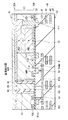
図1は、本開示の第1の実施の形態に係る固体撮像素子10の断面構成を表したものである。この固体撮像素子10は、例えばデジタルスチルカメラ,ビデオカメラ等の電子機器に用いられるCMOSイメージセンサなどの固体撮像装置(後述)において一つの画素を構成するものである。
(First embodiment)
FIG. 1 illustrates a cross-sectional configuration of a solid-
この固体撮像素子10は、例えば、一つの光電変換素子20と、二つのフォトダイオードPD1,PD2とを半導体基板30の厚み方向に積層した、いわゆる縦方向分光型のものである。光電変換素子20は、半導体基板30の第1面(裏面)30A側に設けられている。フォトダイオードPD1,PD2は、半導体基板30内に設けられ、半導体基板30の厚み方向に積層されている。
The solid-
光電変換素子20と、フォトダイオードPD1,PD2とは、互いに異なる波長域の光を選択的に検出して光電変換を行う。具体的には、光電変換素子20は、緑(G)の色信号を取得する。フォトダイオードPD1,PD2は、吸収係数の違いにより、それぞれ、青(B)および赤(R)の色信号を取得する。これにより、この固体撮像素子10では、カラーフィルタを用いることなく一つの画素において複数種類の色信号を取得可能となっている。
The
なお、本実施の形態では、光電変換によって生じる電子およびホールの対のうち、電子を信号電荷として読み出す場合(N型半導体領域を光電変換層とする場合)について説明する。また、図中において、「P」「N」に付した「+(プラス)」は、P型またはN型の不純物濃度が高いことを表し、「++」はP型またはN型の不純物濃度が「+」よりも更に高いことを表している。 Note that in this embodiment, a case where an electron is read out as a signal charge from a pair of electrons and holes generated by photoelectric conversion (when an N-type semiconductor region is used as a photoelectric conversion layer) will be described. In the figure, “+ (plus)” added to “P” and “N” indicates that the P-type or N-type impurity concentration is high, and “++” indicates that the P-type or N-type impurity concentration is high. It is higher than “+”.
半導体基板30の第2面(表面)30Bには、例えば、フローティングディフュージョン(浮遊拡散層)FD1,FD2,FD3と、縦型トランジスタ(転送トランジスタ)Tr1と、転送トランジスタTr2と、アンプトランジスタ(変調素子)AMPと、リセットトランジスタRSTと、多層配線40とが設けられている。多層配線40は、例えば、配線層41,42,43を絶縁膜44内に積層した構成を有している。
On the second surface (front surface) 30B of the
なお、図面では、半導体基板30の第1面30A側を光入射側S1、第2面30B側を配線層側S2と表している。
In the drawing, the
光電変換素子20は、例えば、下部の透明電極21と、光電変換膜22と、上部の透明電極23とを、半導体基板30の第1面30Aの側からこの順に積層した構成を有している。透明電極21は、一つ一つの固体撮像素子10ごとに分離されている。光電変換膜22および透明電極23は、複数の固体撮像素子10に共通した連続層として設けられている。半導体基板30の第1面30Aと透明電極21との間には、例えば、固定電荷を有する膜24と、絶縁性を有する誘電体層25と、層間絶縁膜26とが設けられている。透明電極23の上には、保護膜27が設けられている。保護膜27の上方には、平坦膜等の光学部材およびオンチップレンズ(いずれも図示せず)が配設されている。
The
半導体基板30の第1面30Aと第2面30Bとの間には、貫通電極50が設けられている。光電変換素子20は、貫通電極50を介して、アンプトランジスタAMPのゲートGampと、フローティングディフュージョンFD3とに接続されている。これにより、この固体撮像素子10では、半導体基板30の第1面30A側の光電変換素子20で生じた電荷を、貫通電極50を介して半導体基板30の第2面30B側に良好に転送し、特性を高めることが可能となっている。
A through
貫通電極50は、光電変換素子20とアンプトランジスタAMPのゲートGampおよびフローティングディフュージョンFD3とのコネクタとしての機能を有すると共に、光電変換素子20において生じた電荷(ここでは電子)の伝送経路となるものである。貫通電極50の下端は、例えば、下部第1コンタクト51を介して、多層配線40の配線層41内の接続部41Aに接続されている。接続部41Aと、アンプトランジスタAMPのゲートGampとは、下部第2コンタクト52により接続されている。接続部41Aと、フローティングディフュージョンFD3とは、下部第3コンタクト53により接続されている。貫通電極50の上端は、例えば、上部コンタクト54を介して下部透明電極21に接続されている。
The through
図2は、固体撮像素子10を、半導体基板30の第2面30Bの側から見た平面構成を表したものであり、四つの固体撮像素子10を二行×二列に配置した例を表している。貫通電極50は、固体撮像素子10の各々に、光電変換素子20ごとに設けられていることが好ましい。すなわち、光電変換素子20の下部の透明電極21が固体撮像素子10ごとに分離されていることに伴い、貫通電極50も光電変換素子20ごとに設けられることになる。
FIG. 2 shows a planar configuration of the solid-
図1および図2に示したように、フローティングディフュージョンFD3の隣には、リセットトランジスタRSTのリセットゲートGrstが配置されていることが好ましい。これにより、フローティングディフュージョンFD3に蓄積された電荷を、リセットトランジスタRSTによりリセットすることが可能となる。 As shown in FIGS. 1 and 2, it is preferable that a reset gate Grst of the reset transistor RST is arranged next to the floating diffusion FD3. As a result, the charge accumulated in the floating diffusion FD3 can be reset by the reset transistor RST.
なお、図2には、光電変換素子20からの電荷を扱うアンプトランジスタAMPおよびリセットトランジスタRSTのみを表している。フォトダイオードPD1,PD2に関する転送トランジスタTr1,Tr2は、図2には図示しないが、空いている領域に適宜設置されている。
FIG. 2 shows only the amplifier transistor AMP and the reset transistor RST that handle charges from the
図1に示した貫通電極50は、半導体基板30を貫通すると共に、分離溝60により半導体基板30とは分離されている。貫通電極50は、例えば、半導体基板30と同じ半導体、例えばシリコン(Si)により構成され、N型またはP型の不純物が注入される(図1では例えばP+)ことにより抵抗値が低減されていることが好ましい。また、貫通電極50の上端部および下端部には、高濃度不純物領域(図1では例えばP++)が設けられ、上部コンタクト54との接続抵抗および下部第1コンタクト51との接続抵抗が更に低減されていることが好ましい。
The through
図1に示したように、分離溝60の外側面61、内側面62および底面63は、絶縁性を有する誘電体層25により被覆されている。誘電体層25は、例えば、分離溝60の外側面61を被覆する外側誘電体層25Aと、分離溝60の内側面62を被覆する内側誘電体層25Bとを有している。外側誘電体層25Aと内側誘電体層25Bとの間には、空洞70が設けられていることが好ましい。つまり、分離溝60は環状または輪状であり、空洞70は分離溝60と同心円をなす環状または輪状である。これにより、貫通電極50と半導体基板30との間に生じる静電容量を低減させ、変換効率を高めると共に遅延(残像)を抑えることが可能となる。
As shown in FIG. 1, the
以下、このことについて説明する。上述したように、貫通電極50はP+シリコンなどの導電性材料により構成され、貫通電極50と半導体基板30との間には誘電体層25が設けられている。貫通電極50は半導体基板30を貫通し、アンプトランジスタAMPおよびフローティングディフュージョンFD3に接続されているので、貫通電極50と半導体基板30との間に生じる静電容量を低減することが望ましい。静電容量を低減させるためには、以下の三つの対応が考えられる。一つ目は、貫通電極50の側壁の面積を減らすことである。二つ目は、貫通電極50と半導体基板30との距離dを増大させることである。三つ目は、貫通電極50と半導体基板30との間の絶縁体の誘電率を下げることである。
This will be described below. As described above, the through
一つ目の貫通電極50の側壁の面積の縮小は、半導体基板30の厚さを薄くしたり、貫通電極50の径を小さくしたりすることで可能となる。しかしながら、フォトダイオードPD1,PD2の領域が小さくなったり、半導体基板30の加工プロセスの難易度が上がる可能性がある。二つ目の貫通電極50と半導体基板30との距離dの増大は、比較的容易な対応であるが、素子面積の拡大につながる。
The area of the side wall of the first through
本実施の形態では、分離溝60内に空洞70を設けることにより、上記の三つ目の対応、つまり貫通電極50と半導体基板30との間の絶縁体の誘電率を下げるようにしたものである。空洞70内には水素や窒素等の気体が存在しているが、例えばTEOS(Tetraethyl orthosilicate)膜等の固体の誘電体に比べてその誘電率は低く、真空の誘電率に近い。そのため、貫通電極50と半導体基板30との間の容量を劇的に低減することが可能となる。
In the present embodiment, by providing the
なお、空洞70のサイズばらつきは、固体撮像素子10が集合した固体撮像装置(後述)内またはウェハ内においてできるだけ小さいことが好ましく、例えばプラスマイナス10%以下であることが好ましい。貫通電極50と半導体基板30との間の容量は、空洞70のサイズに敏感であるからである。
Note that the size variation of the
また、この固体撮像素子10では、図1に示したように、分離溝60の外側面61の半導体基板30内には、貫通電極50と同じ導電型(N型またはP型)の不純物領域(図1ではP+)が設けられていることが好ましい。更に、分離溝60の外側面61、内側面62および底面63と、半導体基板30の第1面30Aとに、固定電荷を有する膜24が設けられていることが好ましい。具体的には、例えば、分離溝60の外側面61の半導体基板30内にP型の不純物領域(図1のP+)を設けると共に、固定電荷を有する膜24として負の固定電荷を有する膜を設けることが好ましい。これにより、暗電流を低減することが可能となる。
In the solid-
以下、このことについて説明する。すなわち、縦方向分光の固体撮像素子10では、貫通電極50および分離溝60を、半導体基板30内のフォトダイオードPD1,PD2に近接させた状態で、光電変換素子20ごとに設ける。貫通電極50および分離溝60の表面は、半導体基板30の表面と異なり、ドライエッチング等で加工した表面となるので、一般的に欠陥準位が多い。そのため、貫通電極50および分離溝60に隣接するフォトダイオードPD1,PD2の暗電流や白点が増加するおそれがある。
This will be described below. In other words, in the solid-
ここでは、暗電流や白点を低減させるため、分離溝60の外側面61の半導体基板30内にP型の不純物領域(図1のP+)を設け、更に、固定電荷を有する膜24として負の固定電荷を有する膜を設けるようにしている。負の固定電荷を有する膜24が誘起する電界により、分離溝60の外側面61にホール蓄積(ホールアキュミュレーション)層が形成される。このホール蓄積層によって、分離溝60の外側面61からの電子の発生が抑制される。また、分離溝60の外側面61から電荷(電子)が発生した場合でも、発生した電子は拡散する途中のホール蓄積層で消滅するので、暗電流が低減される。
Here, in order to reduce dark current and white spots, a P-type impurity region (P + in FIG. 1) is provided in the
以下、各部の構成や材料等について説明する。 Hereinafter, the configuration and materials of each part will be described.
光電変換素子20は、例えば495nm〜570nmの波長域の一部または全部の波長域に対応する緑色光を光電変換するものである。透明電極21,23は、例えば、光透過性を有する導電膜により構成され、例えばITO(インジウムスズ酸化物)により構成されている。光電変換膜22は、選択的な波長域の光を光電変換する一方、他の波長域の光を透過させる有機光電変換材料よりなる有機膜である。光電変換膜22は、例えば、ローダーミン系色素、メラシアニン系色素、キナクリドン等を含む有機光電変換材料により構成されている。なお、光電変換素子20には、透明電極21,23および光電変換膜22以外にも、下地層,電子ブロック層,バッファ層などの図示しない他の層が設けられていてもよい。
The
固定電荷を有する膜24は、正の固定電荷を有する膜でもよいし、負の固定電荷を有する膜でもよい。負の固定電荷を有する膜の材料としては、酸化ハフニウム、酸化アルミニウム、酸化ジルコニウム、酸化タンタル、酸化チタンなどが挙げられる。また上記以外の材料としては酸化ランタン、酸化プラセオジム、酸化セリウム、酸化ネオジム、酸化プロメチウム、酸化サマリウム、酸化ユウロピウム、酸化ガドリニウム、酸化テルビウム、酸化ジスプロシウム、酸化ホルミウム、酸化ツリウム、酸化イッテルビウム、酸化ルテチウム、酸化イットリウム、窒化アルミニウム膜、酸窒化ハフニウム膜または酸窒化アルミニウム膜なども可能である。
The
固定電荷を有する膜24は、2種類以上の膜を積層した構成を有していてもよい。それにより、例えば負の固定電荷を有する膜の場合にはホール蓄積層としての機能を更に高めることが可能である。
The
誘電体層25の材料は特に限定されないが、例えば、シリコン酸化膜、TEOS、シリコン窒化膜、シリコン酸窒化膜を含む。
The material of the
層間絶縁膜26は、例えば、シリコン酸化膜により構成されている。保護膜27は、例えば、シリコン窒化膜により構成されている。
The
半導体基板30は、例えば、n型のシリコン(Si)基板により構成され、所定領域にpウェル31を有している。pウェル31の第2面30Bには、上述した縦型トランジスタTr1,転送トランジスタTr2,アンプトランジスタAMP,リセットトランジスタRST等が設けられている。また、半導体基板30の周辺部には、ロジック回路等からなる周辺回路(図示せず)が設けられている。
The
フォトダイオードPD1,PD2は、それぞれ、半導体基板30の所定領域にPN接合を有する。フォトダイオードPD1,PD2は、シリコン基板において光の入射深さに応じて吸収される光の波長が異なることを利用して縦方向に光を分光することを可能としたものである。フォトダイオードPD1は、青色光を選択的に検出して青色に対応する信号電荷を蓄積させるものであり、青色光を効率的に光電変換可能な深さに設置されている。フォトダイオードPD2は、赤色光を選択的に検出して赤色に対応する信号電荷を蓄積させるものであり、赤色光を効率的に光電変換可能な深さに設置されている。なお、青(B)は、例えば450nm〜495nmの波長域、赤(R)は、例えば620nm〜750nmの波長域にそれぞれ対応する色であり、フォトダイオードPD1,PD2はそれぞれ、各波長域のうちの一部または全部の波長域の光を検出可能となっていればよい。
Each of the photodiodes PD1 and PD2 has a PN junction in a predetermined region of the
フォトダイオードPD1は、例えば、ホール蓄積層となるP+領域と、電子蓄積層となるN領域とを含んで構成されている。フォトダイオードPD2は、例えば、ホール蓄積層となるP+領域と、電子蓄積層となるN領域とを有する(P−N−Pの積層構造を有する)。フォトダイオードPD1のN領域は、縦型トランジスタTr1に接続されている。フォトダイオードPD1のP+領域は、縦型トランジスタTr1に沿って屈曲し、フォトダイオードPD2のP+領域につながっている。 The photodiode PD1 includes, for example, a P + region that becomes a hole accumulation layer and an N region that becomes an electron accumulation layer. The photodiode PD2 includes, for example, a P + region serving as a hole accumulation layer and an N region serving as an electron accumulation layer (having a PNP structure). The N region of the photodiode PD1 is connected to the vertical transistor Tr1. The P + region of the photodiode PD1 is bent along the vertical transistor Tr1 and connected to the P + region of the photodiode PD2.
縦型トランジスタTr1は、フォトダイオードPD1において発生し、蓄積された、青色に対応する信号電荷(本実施の形態では電子)を、フローティングディフュージョンFD1に転送する転送トランジスタである。フォトダイオードPD1は半導体基板30の第2面30Bから深い位置に形成されているので、フォトダイオードPD1の転送トランジスタは縦型トランジスタTr1により構成されていることが好ましい。
The vertical transistor Tr1 is a transfer transistor that transfers signal charges (electrons in the present embodiment) corresponding to blue generated and accumulated in the photodiode PD1 to the floating diffusion FD1. Since the photodiode PD1 is formed at a deep position from the
転送トランジスタTr2は、フォトダイオードPD2において発生し、蓄積された、赤色に対応する信号電荷(本実施の形態では電子)を、フローティングディフュージョンFD2に転送するものであり、例えばMOSトランジスタにより構成されている。 The transfer transistor Tr2 transfers signal charges (electrons in the present embodiment) generated and accumulated in the photodiode PD2 corresponding to red to the floating diffusion FD2, and is configured by, for example, a MOS transistor. .
アンプトランジスタAMPは、光電変換素子20で生じた電荷量を電圧に変調する変調素子であり、例えばMOSトランジスタにより構成されている。
The amplifier transistor AMP is a modulation element that modulates the amount of charge generated in the
リセットトランジスタRSTは、光電変換素子20からフローティングディフュージョンFD3に転送された電荷をリセットするものであり、例えばMOSトランジスタにより構成されている。
The reset transistor RST resets the charge transferred from the
下部第1〜第3コンタクト51〜53および上部コンタクト54は、例えば、PDAS(Phosphorus Doped Amorphous Silicon)等のドープされたシリコン材料、または、アルミニウム、タングステン、チタン、コバルト、ハフニウム、タンタル等の金属材料により構成されている。
The lower first to
この固体撮像素子10は、例えば、次のようにして製造することができる。
For example, the solid-
図3ないし図8は、この固体撮像素子10の製造方法を工程順に表したものである。まず、図3に示したように、半導体基板30内に、第1の導電型のウェルとして例えばpウェル31を形成し、このpウェル31内に第2の導電型(例えばN型)のフォトダイオードPD1,PD2を形成する。半導体基板30の第1面30A近傍にはP+領域を形成する。
3 to 8 show the manufacturing method of the solid-
また、同じく図3に示したように、貫通電極50および分離溝60の形成予定領域に、半導体基板30の第1面30Aから第2面30Bまで貫通する不純物領域(P+領域)を形成する。更に、貫通電極50の上端部および下端部の形成予定領域には高濃度不純物領域(P++領域)を形成する。
Similarly, as shown in FIG. 3, an impurity region (P + region) penetrating from the
半導体基板30の第2面30Bには、同じく図3に示したように、フローティングディフュージョンFD1〜FD3となるN+領域を形成したのち、ゲート絶縁膜32と、縦型トランジスタTr1、転送トランジスタTr2、アンプトランジスタAMPおよびリセットトランジスタRSTの各ゲートを含むゲート配線33とを形成する。これにより、縦型トランジスタTr1、転送トランジスタTr2、アンプトランジスタAMPおよびリセットトランジスタRSTを形成する。更に、半導体基板30の第2面30B上に、下部第1〜第3コンタクト51〜53、接続部41Aを含む配線層41〜43、絶縁膜44からなる多層配線40を形成する。
As shown in FIG. 3, the N + region to be the floating diffusions FD1 to FD3 is formed on the
半導体基板30の基体としては、例えば、半導体基板30と、埋込み酸化膜(図示せず)と、保持基板(図示せず)とを積層したSOI(Silicon on Insulator)基板を用いる。埋込み酸化膜および保持基板は、図3には図示しないが、半導体基板30の第1面30Aに接合されている。イオン注入後、アニール処理を行う。
As the base of the
次いで、図4に示したように、半導体基板30の第2面30B側(多層配線40)に支持基板(図示せず)または他の半導体基体等を接合して、上下反転する。続いて、半導体基板30をSOI基板の埋込み酸化膜および保持基板から分離し、半導体基板30の第1面30Aを露出させる。以上の工程は、イオン注入およびCVD(Chemical Vapor Deposition)等、通常のCMOSプロセスで使用されている技術にて行うことが可能である。
Next, as shown in FIG. 4, a support substrate (not shown) or another semiconductor substrate or the like is bonded to the
そののち、図5に示したように、例えばドライエッチングにより半導体基板30を第1面30A側から加工し、輪状あるいは環状の分離溝60を形成する。
After that, as shown in FIG. 5, the
分離溝60の深さは、図5の矢印D60Aに示したように、半導体基板30を第1面30Aから第2面30Bまで貫通してゲート絶縁膜32に達することが好ましい。更に、分離溝60の底面63での絶縁効果をより高めるためには、分離溝60は、図5の矢印D60Bに示したように、半導体基板30およびゲート絶縁膜32を貫通して多層配線40の絶縁膜44に達することが好ましい。図5には、分離溝60が半導体基板30およびゲート絶縁膜32を貫通している場合を表している。
The depth of the
分離溝60を形成したのち、図6に示したように、分離溝60の外側面61、内側面62および底面63と、半導体基板30の第1面30Aとに、例えば負の固定電荷を有する膜24を形成する。負の固定電荷を有する膜24として、2種類以上の膜を積層してもよい。それにより、ホール蓄積層としての機能をより高めることが可能となる。
After forming the
負の固定電荷を有する膜24を形成したのち、図7に示したように、外側誘電体層25Aおよび内側誘電体層25Bを有する誘電体層25を形成する。このとき、誘電体層25の膜厚および成膜条件を適切に調節することで、分離溝60内において、外側誘電体層25Aと内側誘電体層25Bとの間に空洞70を形成する。
After forming the
誘電体層25および空洞70を形成したのち、図8に示したように、層間絶縁膜26および上部コンタクト54を形成し、上部コンタクト54を貫通電極50の上端に接続する。そののち、図1に示したように、下部透明電極21,光電変換膜22および上部透明電極23、保護膜27を形成する。最後に、平坦膜等の光学部材およびオンチップレンズ(図示せず)を配設する。以上により、図1に示した固体撮像素子10が完成する。
After the
この固体撮像素子10では、光電変換素子20に、オンチップレンズ(図示せず)を介して光が入射すると、この光は、光電変換素子20、フォトダイオードPD1,PD2の順に通過し、その通過過程において緑、青、赤の色光毎に光電変換される。以下、各色の信号取得動作について説明する。
In this solid-
(光電変換素子20による緑色信号の取得)
光電変換素子10へ入射した光のうち、まず、緑色光が、光電変換素子20において選択的に検出(吸収)され、光電変換される。
(Acquisition of green signal by photoelectric conversion element 20)
Of the light incident on the
光電変換素子20は、貫通電極50を介して、アンプトランジスタAMPのゲートGampとフローティングディフュージョンFD3とに接続されている。よって、光電変換素子20で発生した電子・ホール対のうちの電子が、透明電極21側から取り出され、貫通電極50を介して半導体基板30の第2面30B側へ転送され、フローティングディフュージョンFD3に蓄積される。これと同時に、アンプトランジスタAMPにより、光電変換素子20で生じた電荷量が電圧に変調される。
The
また、フローティングディフュージョンFD3の隣には、リセットトランジスタRSTのリセットゲートGrstが配置されている。これにより、フローティングディフュージョンFD3に蓄積された電荷は、リセットトランジスタRSTによりリセットされる。 Further, a reset gate Grst of the reset transistor RST is arranged next to the floating diffusion FD3. Thereby, the electric charge accumulated in the floating diffusion FD3 is reset by the reset transistor RST.
ここでは、光電変換素子20が、貫通電極50を介して、アンプトランジスタAMPだけでなくフローティングディフュージョンFD3にも接続されているので、フローティングディフュージョンFD3に蓄積された電荷をリセットトランジスタRSTにより容易にリセットすることが可能となる。
Here, since the
これに対して、貫通電極50とフローティングディフュージョンFD3とが接続されていない場合には、フローティングディフュージョンFD3に蓄積された電荷をリセットすることが困難となり、大きな電圧をかけて透明電極23側へ引き抜くことになる。そのため、光電変換膜22がダメージを受けるおそれがある。また、短時間でのリセットを可能とする構造は暗時ノイズの増大を招き、トレードオフとなるため、この構造は困難である。
On the other hand, when the through
(フォトダイオードPD1,PD2による青色信号,赤色信号の取得)
続いて、光電変換素子20を透過した光のうち、青色光はフォトダイオードPD1、赤色光はフォトダイオードPD2において、それぞれ順に吸収され、光電変換される。フォトダイオードPD1では、入射した青色光に対応した電子がフォトダイオードPD1のN領域に蓄積され、蓄積された電子は、縦型トランジスタTr1によりフローティングディフュージョンFD1へと転送される。同様に、フォトダイオードPD2では、入射した赤色光に対応した電子がフォトダイオードPD2のN領域に蓄積され、蓄積された電子は、転送トランジスタTr2によりフローティングディフュージョンFD2へと転送される。
(Acquisition of blue and red signals by photodiodes PD1 and PD2)
Subsequently, among the light transmitted through the
このように本実施の形態では、光電変換素子20を、貫通電極50を介して、アンプトランジスタAMPのゲートGampとフローティングディフュージョンFD3とに接続するようにしたので、半導体基板30の第1面30A側の光電変換素子20で生じた電荷を、貫通電極50を介して半導体基板30の第2面30B側に良好に転送し、特性を高めることが可能となる。
As described above, in the present embodiment, the
また、貫通電極50と半導体基板30とを、分離溝60、外側誘電体層25A、内側誘電体層25Bおよび空洞70で分離するようにしたので、貫通電極50と半導体基板30との間に生じる静電容量を低減し、変換効率などの特性を更に向上させることが可能となる。
Further, since the through
更に、フローティングディフュージョンFD3の隣に、リセットトランジスタRSTのリセットゲートGrstを配置するようにしたので、フローティングディフュージョンFD3に蓄積された電荷を、リセットトランジスタRSTにより容易にリセットすることが可能となる。よって、光電変換膜22のダメージを抑え、信頼性を向上させることが可能となる。また、暗時ノイズを増大させることなく短時間でのリセットが可能となる。
Furthermore, since the reset gate Grst of the reset transistor RST is arranged next to the floating diffusion FD3, the charge accumulated in the floating diffusion FD3 can be easily reset by the reset transistor RST. Therefore, damage to the
(第2の実施の形態)
図9は、本開示の第2の実施の形態に係る固体撮像素子10Aの断面構成を表したものである。この固体撮像素子10Aは、貫通電極50を金属または導電性材料により構成したことを除いては、上記第1の実施の形態と同様の構成、作用および効果を有している。よって、対応する構成要素には同一の符号を付して説明する。
(Second Embodiment)
FIG. 9 illustrates a cross-sectional configuration of a solid-state imaging element 10A according to the second embodiment of the present disclosure. This solid-state imaging device 10A has the same configuration, operation, and effects as those of the first embodiment except that the through
この固体撮像素子10Aは、第1の実施の形態と同様に、例えば、一つの光電変換素子20と、二つのフォトダイオードPD1,PD2とを半導体基板30の厚み方向に積層した、いわゆる縦方向分光型のものである。光電変換素子20は、半導体基板30の第1面(裏面)30A側に設けられている。フォトダイオードPD1,PD2は、半導体基板30内に設けられ、半導体基板30の厚み方向に積層されている。
As in the first embodiment, this solid-state imaging device 10A is, for example, a so-called longitudinal spectrum in which one
光電変換素子20、フォトダイオードPD1,PD2および半導体基板30は、第1の実施の形態と同様に構成されている。フローティングディフュージョンFD1〜FD3、縦型トランジスタTr1、転送トランジスタTr2、アンプトランジスタAMPと、リセットトランジスタRSTおよび多層配線40は、第1の実施の形態と同様に構成されている。
The
半導体基板30の第1面30Aと第2面30Bとの間には、第1の実施の形態と同様に、貫通電極50が設けられている。光電変換素子20は、貫通電極50を介して、アンプトランジスタAMPのゲートGampと、フローティングディフュージョンFD3とに接続されている。これにより、この固体撮像素子10Aでは、第1の実施の形態と同様に、半導体基板30の第1面30A側の光電変換素子20で生じた電荷を、貫通電極50を介して半導体基板30の第2面30B側に良好に転送し、特性を向上させることが可能となっている。
Similar to the first embodiment, a through
貫通電極50の近傍には、第1の実施の形態と同様に、フローティングディフュージョンFD3が配置されている。フローティングディフュージョンFD3の隣には、リセットトランジスタRSTのリセットゲートGrstが配置されていることが好ましい。これにより、フローティングディフュージョンFD3に蓄積された電荷を、リセットトランジスタRSTによりリセットすることが可能となる。
A floating diffusion FD3 is disposed in the vicinity of the through
本実施の形態では、貫通電極50は、上述したように、金属または導電性材料により構成されている。これにより、貫通電極50の抵抗値を更に低減すると共に、貫通電極50と下部第1〜第3コンタクト51〜53および上部コンタクト54との接続抵抗を更に低減することが可能となる。よって、半導体基板30の第1面30A側の光電変換素子20で生じた電荷を、貫通電極50を介して半導体基板30の第2面30B側に更に良好に転送し、特性を更に向上させることが可能となる。貫通電極50を構成する金属または導電性材料としては、アルミニウム、タングステン、チタン、コバルト、ハフニウム、タンタルなどが挙げられる。
In the present embodiment, the through
貫通電極50と半導体基板30との間には、第1の実施の形態と同様に、分離溝60が設けられていることが好ましい。分離溝60の外側面61、内側面62および底面63は、絶縁性を有する誘電体層25により被覆されていることが好ましい。分離溝60の外側面61を被覆する外側誘電体層25Aと、分離溝60の内側面62を被覆する内側誘電体層25Bとの間には、空洞70が設けられていることが好ましい。これにより、貫通電極50と半導体基板30との間に生じる静電容量を低減させ、変換効率を高めると共に遅延(残像)を抑えることが可能となる。
As in the first embodiment, a
また、この固体撮像素子10Aでは、第1の実施の形態と同様に、分離溝60の外側面61の半導体基板30内には、不純物領域(図9ではP+)が設けられていることが好ましい。更に、分離溝60の外側面61、内側面62および底面63と、半導体基板30の第1面30Aとに、固定電荷を有する膜24が設けられていることが好ましい。具体的には、例えば、分離溝60の外側面61の半導体基板30内にP型の不純物領域(図9のP+)を設けると共に、固定電荷を有する膜24として負の固定電荷を有する膜を設けることが好ましい。これにより、暗電流を低減することが可能となる。
Further, in this solid-state imaging device 10A, it is preferable that an impurity region (P + in FIG. 9) is provided in the
固定電荷を有する膜24は、第1の実施の形態と同様に、正の固定電荷を有する膜でもよいし、負の固定電荷を有する膜でもよい。負の固定電荷を有する膜の材料としては、酸化ハフニウム、酸化アルミニウム、酸化ジルコニウム、酸化タンタル、酸化チタンなどが挙げられる。また上記以外の材料としては酸化ランタン、酸化プラセオジム、酸化セリウム、酸化ネオジム、酸化プロメチウム、酸化サマリウム、酸化ユウロピウム、酸化ガドリニウム、酸化テルビウム、酸化ジスプロシウム、酸化ホルミウム、酸化ツリウム、酸化イッテルビウム、酸化ルテチウム、酸化イットリウム、窒化アルミニウム膜、酸窒化ハフニウム膜または酸窒化アルミニウム膜なども可能である。
The
固定電荷を有する膜24は、第1の実施の形態と同様に、2種類以上の膜を積層した構成を有していてもよい。それにより、例えば負の固定電荷を有する膜の場合にはホール蓄積層としての機能を更に高めることが可能である。
The
誘電体層25の材料は特に限定されないが、第1の実施の形態と同様に、例えば、シリコン酸化膜、TEOS、シリコン窒化膜、シリコン酸窒化膜を含む。
The material of the
下部第1〜第3コンタクト51〜53および上部コンタクト54は、第1の実施の形態と同様に、例えば、PDAS等のドープされたシリコン材料、または、アルミニウム、タングステン、チタン、コバルト、ハフニウム、タンタル等の金属材料により構成されている。
The lower first to
この固体撮像素子10Aは、例えば、次のようにして製造することができる。 This solid-state imaging device 10A can be manufactured as follows, for example.
図10ないし図18は、この固体撮像素子10Aの製造方法を工程順に表したものである。まず、第1の実施の形態と同様にして、図3に示した工程により、半導体基板30内に、第1の導電型のウェルとして例えばpウェル31を形成し、このpウェル31内に第2の導電型(例えばN型)のフォトダイオードPD1,PD2を形成する。半導体基板30の第1面30A近傍にはP+領域を形成する。
10 to 18 show the manufacturing method of the solid-state imaging device 10A in the order of steps. First, in the same manner as in the first embodiment, a p-
また、第1の実施の形態と同様に、同じく図3に示した工程により、貫通電極50および分離溝60の形成予定領域に、半導体基板30の第1面30Aから第2面30Bまで貫通する不純物領域(P+領域)を形成する。なお、本実施の形態では、貫通電極50を金属または導電性材料により構成するので、貫通電極50の上端部および下端部の高濃度不純物領域(P++領域)は不要である。
Similarly to the first embodiment, the through-
半導体基板30の第2面30Bには、第1の実施の形態と同様に、同じく図3に示し工程により、フローティングディフュージョンFD1〜FD3となるN+領域を形成したのち、ゲート絶縁膜32と、縦型トランジスタTr1、転送トランジスタTr2、アンプトランジスタAMPおよびリセットトランジスタRSTの各ゲートを含むゲート配線33とを形成する。これにより、縦型トランジスタTr1、転送トランジスタTr2、アンプトランジスタAMPおよびリセットトランジスタRSTを形成する。更に、半導体基板30の第2面30B上に、下部第1〜第3コンタクト51〜53、接続部41Aを含む配線層41〜43、絶縁膜44からなる多層配線40を形成する。
Similarly to the first embodiment, N + regions to be the floating diffusions FD1 to FD3 are formed on the
半導体基板30の基体としては、第1の実施の形態と同様に、例えばSOI基板を用いる。イオン注入後、アニール処理を行う。
As the base of the
次いで、図10に示したように、半導体基板30の第2面30B側(多層配線40)に支持基板(図示せず)または他の半導体基体等を接合して、上下反転する。続いて、半導体基板30をSOI基板の埋込み酸化膜および保持基板から分離し、半導体基板30の第1面30Aを露出させる。以上の工程は、イオン注入およびCVD等、通常のCMOSプロセスで使用されている技術にて行うことが可能である。
Next, as shown in FIG. 10, a support substrate (not shown) or another semiconductor substrate is joined to the
そののち、図11に示したように、例えばドライエッチングにより半導体基板30を第1面30A側から加工し、半導体基板30を貫通する環状または輪状の分離溝60を形成する。
After that, as shown in FIG. 11, the
分離溝60を形成したのち、図12に示したように、分離溝60の外側面61および底面63と、半導体基板30の第1面30Aとに、絶縁膜80を成膜する。絶縁膜80の材料としては、TEOS,ALD法により成膜されたSiO膜またはSiN膜等を用いることが可能である。
After forming the
続いて、図13に示したように、ドライエッチング等により絶縁膜80を後退させる。
Subsequently, as shown in FIG. 13, the insulating
そののち、図14に示したように、分離溝60に金属材料膜50Aを埋め込む。
After that, as shown in FIG. 14, the
金属材料膜50Aを埋め込んだのち、図15に示したように、ドライエッチングまたはCMP(Chemical Mechanical Polishing)により、金属材料膜50Aを後退もしくは平坦化させて、貫通電極50を形成する。その際、分離溝60の入口付近ではエッチバックにより絶縁膜80の厚みが薄くなっているので、絶縁膜80の厚みが確保されているところまで金属材料膜50Aを後退させることが好ましい。これにより、貫通電極50と半導体基板30とのショートを抑えることが可能となる。
After embedding the
貫通電極50を形成したのち、図16に示したように、絶縁膜80を剥離する。
After the through
絶縁膜80を剥離したのち、図17に示したように、分離溝60の外側面61、内側面62および底面63と、半導体基板30の第1面30Aとに、例えば負の固定電荷を有する膜24を形成する。負の固定電荷を有する膜24としては、2種類以上の膜を積層してもよい。それにより、ホール蓄積層としての機能をより高めることが可能となる。
After peeling off the insulating
負の固定電荷を有する膜24を形成したのち、同じく図17に示したように、誘電体層25を形成する。このとき、誘電体層25の膜厚および成膜条件を適切に調節することで、分離溝60内に空洞70を形成する。なお、誘電体層25の表面をCMP等で平坦化してもよい。
After the
誘電体層25および空洞70を形成したのち、図18に示したように、層間絶縁膜26および上部コンタクト54を形成し、上部コンタクト54を貫通電極50の上端に接続する。そののち、図9に示したように、下部透明電極21,光電変換膜22および上部透明電極23、保護膜27を形成する。最後に、平坦膜等の光学部材およびオンチップレンズ(図示せず)を配設する。以上により、図9に示した固体撮像素子10Aが完成する。
After forming the
この固体撮像素子10Aでは、光電変換素子20に、オンチップレンズ(図示せず)を介して光が入射すると、この光は、光電変換素子20、フォトダイオードPD1,PD2の順に通過し、その通過過程において緑、青、赤の色光毎に光電変換され、第1の実施の形態と同様にして各色の信号が取得される。
In the solid-state imaging device 10A, when light is incident on the
ここでは、貫通電極50が金属または導電性材料により構成されているので、貫通電極50の抵抗値が低減され、特性がより向上する。
Here, since the through
このように本実施の形態では、貫通電極50を金属または導電性材料により構成するようにしたので、貫通電極50の抵抗値を低減し、特性をより高めることが可能となる。
Thus, in this embodiment, since the through
(変形例1)
図19は、変形例1に係る固体撮像素子10Bの断面構成を表したものである。この固体撮像素子10Bは、誘電体層25と貫通電極50との間、および誘電体層25と半導体基板30との間に、熱酸化膜34を設けたものである。熱酸化膜34は、半導体基板30のシリコンを熱酸化させた酸化シリコン膜、酸化窒化シリコン、高誘電体絶縁膜などにより構成することが可能である。このことを除いては、この固体撮像素子10Bは、上記第1の実施の形態と同様の構成、作用および効果を有している。また、この固体撮像素子10Bは、分離溝60の外側面61および内側面62に熱酸化膜34を設けることを除いては、第1の実施の形態と同様にして製造することができる。
(Modification 1)
FIG. 19 illustrates a cross-sectional configuration of a solid-state imaging element 10B according to the first modification. In the solid-state imaging device 10B, a
(第3の実施の形態)
図20は、本開示の第3の実施の形態に係る固体撮像素子10Cの断面構成を表したものである。この固体撮像素子10Cは、分離溝60を、絶縁性を有する誘電体層25で充填することにより、貫通電極50と半導体基板30との間に生じる静電容量を低減し、変換効率などの特性を更に向上させるようにしたものである。このことを除いては、この固体撮像素子10Cは、上記第1の実施の形態と同様の構成、作用および効果を有している。
(Third embodiment)
FIG. 20 illustrates a cross-sectional configuration of a solid-state imaging element 10C according to the third embodiment of the present disclosure. In this solid-state imaging device 10C, the
この固体撮像素子10Cは、例えば次のようにして製造することができる。 The solid-state imaging device 10C can be manufactured, for example, as follows.
図21および図22は、この固体撮像素子10Cの製造方法を工程順に表したものである。なお、第1の実施の形態と重複する工程については、図3ないし図6を参照して説明する。 21 and 22 show the manufacturing method of the solid-state imaging device 10C in the order of steps. In addition, the process which overlaps with 1st Embodiment is demonstrated with reference to FIG. 3 thru | or FIG.
まず、第1の実施の形態と同様にして、図3に示した工程により、半導体基板30内に、第1の導電型のウェルとして例えばpウェル31を形成し、このpウェル31内に第2の導電型(例えばN型)のフォトダイオードPD1,PD2を形成する。半導体基板30の第1面30A近傍にはP+領域を形成する。
First, in the same manner as in the first embodiment, a p-
また、第1の実施の形態と同様にして、同じく図3に示した工程により、貫通電極50および分離溝60の形成予定領域に、半導体基板30の第1面30Aから第2面30Bまで貫通する不純物領域(P+領域)を形成する。更に、貫通電極50の上端部および下端部の形成予定領域には高濃度不純物領域(P++領域)を形成する。
In the same manner as in the first embodiment, the through-
半導体基板30の第2面30Bには、第1の実施の形態と同様に、同じく図3に示した工程により、フローティングディフュージョンFD1〜FD3となるN+領域を形成したのち、ゲート絶縁膜32と、縦型トランジスタTr1、転送トランジスタTr2、アンプトランジスタAMPおよびリセットトランジスタRSTの各ゲートを含むゲート配線33とを形成する。これにより、縦型トランジスタTr1、転送トランジスタTr2、アンプトランジスタAMPおよびリセットトランジスタRSTを形成する。更に、半導体基板30の第2面30B上に、下部第1〜第3コンタクト51〜53、接続部41Aを含む配線層41〜43、絶縁膜44からなる多層配線40を形成する。
Similarly to the first embodiment, after forming N + regions to be the floating diffusions FD1 to FD3 on the
半導体基板30の基体としては、第1の実施の形態と同様に、例えばSOI基板を用いる。イオン注入後、アニール処理を行う。
As the base of the
次いで、第1の実施の形態と同様に、図4に示した工程により、半導体基板30の第2面30B側(多層配線40)に支持基板(図示せず)または他の半導体基体等を接合して、上下反転する。続いて、半導体基板30をSOI基板の埋込み酸化膜および保持基板から分離し、半導体基板30の第1面30Aを露出させる。以上の工程は、イオン注入およびCVD等、通常のCMOSプロセスで使用されている技術にて行うことが可能である。
Next, as in the first embodiment, a supporting substrate (not shown) or another semiconductor substrate is bonded to the
そののち、第1の実施の形態と同様に、図5に示した工程により、例えばドライエッチングにより半導体基板30を第1面30A側から加工し、環状または輪状の分離溝60を形成する。
After that, as in the first embodiment, the
分離溝60を形成したのち、第1の実施の形態と同様に、図6に示した工程により、分離溝60の外側面61、内側面62および底面63と、半導体基板30の第1面30Aとに、例えば負の固定電荷を有する膜24を形成する。負の固定電荷を有する膜24としては、2種類以上の膜を積層してもよい。それにより、ホール蓄積層としての機能をより高めることが可能となる。
After forming the
負の固定電荷を有する膜24を形成したのち、図21に示したように、分離溝60を誘電体層25で充填する。
After the
誘電体層25を形成したのち、図22に示したように、層間絶縁膜26および上部コンタクト54を形成し、上部コンタクト54を貫通電極50の上端に接続する。そののち、図20に示したように、下部透明電極21,光電変換膜22および上部透明電極23、保護膜27を形成する。最後に、平坦膜等の光学部材およびオンチップレンズ(図示せず)を配設する。以上により、図20に示した固体撮像素子10Cが完成する。
After forming the
(第4の実施の形態)
図23は、本開示の第4の実施の形態に係る固体撮像素子10Dの断面構成を表したものである。この固体撮像素子10Dは、分離溝60を、絶縁性を有する誘電体層25で充填することにより、貫通電極50と半導体基板30との間に生じる静電容量を低減し、変換効率などの特性を更に向上させるようにしたものである。このことを除いては、この固体撮像素子10Dは、上記第2の実施の形態と同様の構成、作用および効果を有している。
(Fourth embodiment)
FIG. 23 illustrates a cross-sectional configuration of a solid-state imaging element 10D according to the fourth embodiment of the present disclosure. In this solid-state imaging device 10D, the
この固体撮像素子10Dは、図24に示したように、誘電体層25で分離溝60を埋め込むことを除いては、第2の実施の形態と同様にして製造することができる。
As shown in FIG. 24, the solid-state imaging element 10D can be manufactured in the same manner as in the second embodiment except that the
(変形例2)
図25は、変形例2に係る固体撮像素子10Eの断面構成を表したものである。この固体撮像素子10Eは、誘電体層25と貫通電極50との間、および誘電体層25と半導体基板30との間に、変形例1と同様の熱酸化膜34を設けたものである。熱酸化膜34は、変形例1と同様に、半導体基板30のシリコンを熱酸化させた酸化シリコン膜、酸化窒化シリコン、高誘電体絶縁膜などにより構成することが可能である。このことを除いては、この固体撮像素子10Eは、上記第3の実施の形態と同様の構成、作用および効果を有している。また、この固体撮像素子10Eは、分離溝60の外側面61および内側面62に熱酸化膜34を設けることを除いては、第3の実施の形態と同様にして製造することができる。
(Modification 2)
FIG. 25 illustrates a cross-sectional configuration of a solid-state imaging element 10E according to
(固体撮像装置の全体構成)
図26は、上記実施の形態において説明した固体撮像素子10,10A〜10Eを画素PXLとして備えた固体撮像装置の全体構成を表したものである。この固体撮像装置1は、例えばCMOSイメージセンサであり、撮像画素領域としての画素部110を有すると共に、例えば行走査部131、水平選択部133、列走査部134およびシステム制御部132からなる回路部130を有している。回路部130は、画素部110の周辺領域に設けられていてもよいし、画素部110と積層されて(画素部110に対向する領域に)設けられていてもよい。
(Overall configuration of solid-state imaging device)
FIG. 26 illustrates an overall configuration of a solid-state imaging device including the solid-
画素部110は、例えば行列状に2次元配置された複数の画素PXLを有している。この画素PXLには、例えば画素行ごとに画素駆動線Lread(具体的には行選択線およびリセット制御線)が配線され、画素列ごとに垂直信号線Lsig が配線されている。画素駆動線Lreadは、画素からの信号読み出しのための駆動信号を伝送するものである。画素駆動線Lreadの一端は、行走査部131の各行に対応した出力端に接続されている。
The
行走査部131は、シフトレジスタやアドレスデコーダ等によって構成され、画素部110の各画素PXLを、例えば行単位で駆動する画素駆動部である。行走査部131によって選択走査された画素行の各画素PXLから出力される信号は、垂直信号線Lsig の各々を通して水平選択部133に供給される。水平選択部133は、垂直信号線Lsig ごとに設けられたアンプや水平選択スイッチ等によって構成されている。
The
列走査部134は、シフトレジスタやアドレスデコーダ等によって構成され、水平選択部133の各水平選択スイッチを走査しつつ順番に駆動するものである。この列走査部134による選択走査により、垂直信号線Lsig の各々を通して伝送される各画素PXLの信号が順番に水平信号線135に伝送され、当該水平信号線135を通して出力される。
The
システム制御部132は、外部から与えられるクロックや、動作モードを指令するデータなどを受け取り、また、固体撮像装置1の内部情報などのデータを出力するものである。システム制御部132はさらに、各種のタイミング信号を生成するタイミングジェネレータを有し、当該タイミングジェネレータで生成された各種のタイミング信号を基に行走査部131、水平選択部133および列走査部134などの駆動制御を行う。
The
(適用例)
上記実施の形態等の固体撮像装置は、例えばデジタルスチルカメラやビデオカメラ等のカメラシステムや、撮像機能を有する携帯電話など、撮像機能を備えたあらゆるタイプの電子機器に適用することができる。図27に、その一例として、電子機器2(カメラ)の概略構成を示す。この電子機器2は、例えば静止画または動画を撮影可能なビデオカメラであり、例えば、固体撮像装置1と、光学系(撮像レンズ)310と、シャッタ装置311と、固体撮像装置1およびシャッタ装置311を駆動する駆動部313(上記回路部130を含む)と、信号処理部312と、ユーザインターフェイス314と、モニタ315とを有する。
(Application example)
The solid-state imaging device of the above-described embodiment can be applied to all types of electronic devices having an imaging function such as a camera system such as a digital still camera and a video camera, and a mobile phone having an imaging function. FIG. 27 shows a schematic configuration of the electronic apparatus 2 (camera) as an example. The
光学系310は、被写体からの像光(入射光)を固体撮像装置1の画素部110へ導くものである。この光学系310は、複数の光学レンズから構成されていてもよい。シャッタ装置311は、固体撮像装置1への光照射期間および遮光期間を制御するものである。駆動部313は、固体撮像装置1の転送動作およびシャッタ装置311のシャッタ動作を制御するものである。信号処理部312は、固体撮像装置1から出力された信号に対し、各種の信号処理を行うものである。信号処理後の映像信号Dout は、モニタ315に出力される。あるいは、映像信号Dout は、メモリーなどの記憶媒体に記憶されてもよい。ユーザインターフェイス314では、撮影シーンの指定(ダイナミックレンジの指定、波長(テラヘルツ、可視、赤外、紫外、X線等)の指定など)が可能であり、この指定(ユーザインターフェイス314からの入力信号)は、駆動部313に送られ、これに基づいて固体撮像装置1において所望の撮像がなされる。
The
以上、実施の形態を挙げて説明したが、本開示は上記実施の形態に限定されるものではなく、種々変形が可能である。例えば、固体撮像素子10の画素回路は、転送トランジスタ、アンプトランジスタおよびリセットトランジスタからなる、計三つのトランジスタを含む3トランジスタ構成でもよいし、これらに選択トランジスタを加えた4トランジスタ構成でもよい。
As described above, the embodiments have been described. However, the present disclosure is not limited to the above-described embodiments, and various modifications can be made. For example, the pixel circuit of the solid-
また、上記実施の形態では、固体撮像装置がカメラに適用される場合を例示したが、これ以外にも、例えば内視鏡、ビジョンチップ(人工網膜)、生体センサなど、光(電磁波)をイメージングする電子機器全般に用いることができる。 In the above-described embodiment, the case where the solid-state imaging device is applied to a camera is exemplified. However, in addition to this, light (electromagnetic waves) is imaged, for example, an endoscope, a vision chip (artificial retina), a biological sensor, or the like. It can be used for all electronic devices.
また上記実施の形態では、裏面照射型の固体撮像素子10を例に挙げて説明したが、表面照射型のものにも本開示は適用可能である。
In the above-described embodiment, the back-illuminated solid-
また、上記実施の形態の固体撮像素子10および固体撮像装置1は、上記実施の形態で説明した各構成要素を全て備えている必要はなく、また逆に他の構成要素を備えていてもよい。
Further, the solid-
なお、本技術は、以下のような構成をとることも可能である。
(1)
半導体基板の第1面側に設けられた光電変換素子と、
前記光電変換素子に接続され、前記半導体基板の前記第1面と第2面との間に設けられた貫通電極と、
前記半導体基板の前記第2面に設けられたアンプトランジスタおよびフローティングディフュージョンと
を有し、
前記光電変換素子は、前記貫通電極を介して、前記アンプトランジスタのゲートと前記フローティングディフュージョンとに接続されている
固体撮像素子。
(2)
前記半導体基板の前記第2面に、リセットゲートを含むリセットトランジスタを有し、
前記リセットゲートは、前記フローティングディフュージョンの隣に設けられている
前記(1)記載の固体撮像素子。
(3)
前記貫通電極は、前記光電変換素子ごとに設けられている
前記(1)または(2)記載の固体撮像素子。
(4)
前記貫通電極は、前記半導体基板を貫通すると共に、分離溝により前記半導体基板と分離されている
前記(1)ないし(3)のいずれかに記載の固体撮像素子。
(5)
前記貫通電極は、N型またはP型の不純物が注入された半導体により構成され、
前記分離溝の外側面の前記半導体基板内に、前記貫通電極と同じ導電型の不純物領域が設けられている
前記(4)記載の固体撮像素子。
(6)
前記貫通電極は、金属または導電性材料により構成されている
前記(4)記載の固体撮像素子。
(7)
前記分離溝は、絶縁性を有する誘電体層により充填されている
前記(4)ないし(6)のいずれかに記載の固体撮像素子。
(8)
前記分離溝の外側面は、外側誘電体層により被覆され、
前記分離溝の内側面は、内側誘電体層により被覆され、
前記外側誘電体層と前記内側誘電体層との間に、空洞が設けられている
前記(4)ないし(6)のいずれかに記載の固体撮像素子。
(9)
前記分離溝の外側面、内側面および底面と、前記半導体基板の前記第1面に、固定電荷を有する膜が設けられている
前記(4)ないし(8)のいずれかに記載の固体撮像素子。
(10)
前記半導体基板内に設けられた1または複数のフォトダイオードを有する
前記(1)ないし(9)のいずれかに記載の固体撮像素子。
(11)
半導体基板の第1面側に設けられた光電変換素子と、
前記光電変換素子に接続され、前記半導体基板の前記第1面と第2面との間に設けられた貫通電極と、
前記貫通電極と前記半導体基板との間に設けられた分離溝と、
前記分離溝を充填し、絶縁性を有する誘電体層と
を備えた固体撮像素子。
(12)
半導体基板の第1面側に設けられた光電変換素子と、
前記光電変換素子に接続され、前記半導体基板の前記第1面と第2面との間に設けられた貫通電極と、
前記貫通電極と前記半導体基板との間に設けられた分離溝と、
前記分離溝の外側面を被覆する外側誘電体層と、
前記分離溝の内側面を被覆する内側誘電体層と、
前記外側誘電体層と前記内側誘電体層との間に設けられた空洞と
を備えた固体撮像素子。
(13)
固体撮像素子を有し、
前記固体撮像素子は、
半導体基板の第1面側に設けられた光電変換素子と、
前記光電変換素子に接続され、前記半導体基板の前記第1面と第2面との間に設けられた貫通電極と、
前記半導体基板の前記第2面に設けられたアンプトランジスタおよびフローティングディフュージョンと
を有し、
前記光電変換素子は、前記貫通電極を介して、前記アンプトランジスタのゲートと前記フローティングディフュージョンとに接続されている
電子機器。
(14)
固体撮像素子を有し、
前記固体撮像素子は、
半導体基板の第1面側に設けられた光電変換素子と、
前記光電変換素子に接続され、前記半導体基板の前記第1面と第2面との間に設けられた貫通電極と、
前記貫通電極と前記半導体基板との間に設けられた分離溝と、
前記分離溝を充填し、絶縁性を有する誘電体層と
を備えた電子機器。
(15)
固体撮像素子を有し、
前記固体撮像素子は、
半導体基板の第1面側に設けられた光電変換素子と、
前記光電変換素子に接続され、前記半導体基板の前記第1面と第2面との間に設けられた貫通電極と、
前記貫通電極と前記半導体基板との間に設けられた分離溝と、
前記分離溝の外側面を被覆する外側誘電体層と、
前記分離溝の内側面を被覆する内側誘電体層と、
前記外側誘電体層と前記内側誘電体層との間に設けられた空洞と
を備えた電子機器。
In addition, this technique can also take the following structures.
(1)
A photoelectric conversion element provided on the first surface side of the semiconductor substrate;
A through electrode connected to the photoelectric conversion element and provided between the first surface and the second surface of the semiconductor substrate;
An amplifier transistor and a floating diffusion provided on the second surface of the semiconductor substrate;
The photoelectric conversion element is connected to the gate of the amplifier transistor and the floating diffusion through the through electrode.
(2)
A reset transistor including a reset gate on the second surface of the semiconductor substrate;
The solid-state imaging device according to (1), wherein the reset gate is provided next to the floating diffusion.
(3)
The said penetration electrode is provided for every said photoelectric conversion element. The solid-state image sensor of the said (1) or (2) description.
(4)
The solid-state imaging device according to any one of (1) to (3), wherein the through electrode penetrates the semiconductor substrate and is separated from the semiconductor substrate by a separation groove.
(5)
The through electrode is made of a semiconductor into which an N-type or P-type impurity is implanted,
The solid-state imaging device according to (4), wherein an impurity region having the same conductivity type as that of the through electrode is provided in the semiconductor substrate on an outer surface of the separation groove.
(6)
The through electrode is made of a metal or a conductive material. The solid-state imaging device according to (4).
(7)
The solid-state imaging element according to any one of (4) to (6), wherein the separation groove is filled with an insulating dielectric layer.
(8)
The outer surface of the separation groove is covered with an outer dielectric layer,
The inner surface of the separation groove is covered with an inner dielectric layer,
The solid-state imaging device according to any one of (4) to (6), wherein a cavity is provided between the outer dielectric layer and the inner dielectric layer.
(9)
The solid-state imaging device according to any one of (4) to (8), wherein a film having a fixed charge is provided on an outer surface, an inner surface, and a bottom surface of the separation groove and on the first surface of the semiconductor substrate. .
(10)
The solid-state imaging device according to any one of (1) to (9), including one or a plurality of photodiodes provided in the semiconductor substrate.
(11)
A photoelectric conversion element provided on the first surface side of the semiconductor substrate;
A through electrode connected to the photoelectric conversion element and provided between the first surface and the second surface of the semiconductor substrate;
A separation groove provided between the through electrode and the semiconductor substrate;
A solid-state imaging device comprising: a dielectric layer filling the separation groove and having an insulating property.
(12)
A photoelectric conversion element provided on the first surface side of the semiconductor substrate;
A through electrode connected to the photoelectric conversion element and provided between the first surface and the second surface of the semiconductor substrate;
A separation groove provided between the through electrode and the semiconductor substrate;
An outer dielectric layer covering the outer surface of the separation groove;
An inner dielectric layer covering the inner surface of the separation groove;
A solid-state imaging device comprising: a cavity provided between the outer dielectric layer and the inner dielectric layer.
(13)
A solid-state image sensor;
The solid-state imaging device is
A photoelectric conversion element provided on the first surface side of the semiconductor substrate;
A through electrode connected to the photoelectric conversion element and provided between the first surface and the second surface of the semiconductor substrate;
An amplifier transistor and a floating diffusion provided on the second surface of the semiconductor substrate;
The electronic device, wherein the photoelectric conversion element is connected to the gate of the amplifier transistor and the floating diffusion through the through electrode.
(14)
A solid-state image sensor;
The solid-state imaging device is
A photoelectric conversion element provided on the first surface side of the semiconductor substrate;
A through electrode connected to the photoelectric conversion element and provided between the first surface and the second surface of the semiconductor substrate;
A separation groove provided between the through electrode and the semiconductor substrate;
An electronic device comprising: a dielectric layer filling the separation groove and having an insulating property.
(15)
A solid-state image sensor;
The solid-state imaging device is
A photoelectric conversion element provided on the first surface side of the semiconductor substrate;
A through electrode connected to the photoelectric conversion element and provided between the first surface and the second surface of the semiconductor substrate;
A separation groove provided between the through electrode and the semiconductor substrate;
An outer dielectric layer covering the outer surface of the separation groove;
An inner dielectric layer covering the inner surface of the separation groove;
An electronic device comprising: a cavity provided between the outer dielectric layer and the inner dielectric layer.
10,10A〜10E…固体撮像素子、20…光電変換素子、21,23…透明電極、22…光電変換膜、24…固定電荷を有する膜、25…誘電体層、25A…外側誘電体層、25B…内側誘電体層、30…半導体基板、30A…第1面、30B…第2面、40…多層配線、41A…接続部、50…貫通電極、51〜53…下部第1〜第3コンタクト、54…上部コンタクト、60…分離溝、61…外側面、62…内側面、63…底面、70…空洞、AMP…アンプトランジスタ、PD1,PD2…フォトダイオード、RST…リセットトランジスタ、Tr1…縦型トランジスタ、Tr2…転送トランジスタ、1…固体撮像装置、2…電子機器。
DESCRIPTION OF
Claims (16)
前記光電変換素子に接続され、前記半導体基板の前記第1面と第2面との間に設けられた貫通電極と、
前記貫通電極と前記半導体基板との間に設けられた分離溝と、
前記分離溝を充填し、絶縁性を有する誘電体層と、
前記分離溝の外側面、内側面および底面と、前記半導体基板の前記第1面とに設けられた固定電荷を有する膜と
を備えた固体撮像素子。 A photoelectric conversion element provided on the first surface side of the semiconductor substrate;
A through electrode connected to the photoelectric conversion element and provided between the first surface and the second surface of the semiconductor substrate;
A separation groove provided between the through electrode and the semiconductor substrate;
A dielectric layer filling the separation groove and having an insulating property ;
A solid-state imaging device comprising an outer surface, an inner surface, and a bottom surface of the separation groove, and a film having a fixed charge provided on the first surface of the semiconductor substrate .
前記リセットゲートは、前記フローティングディフュージョンの隣に設けられている
請求項1記載の固体撮像素子。 An amplifier transistor, a floating diffusion, and a reset transistor including a reset gate on the second surface of the semiconductor substrate;
The solid-state imaging device according to claim 1, wherein the reset gate is provided next to the floating diffusion.
請求項1記載の固体撮像素子。 The solid-state imaging element according to claim 1, wherein the through electrode is provided for each photoelectric conversion element.
請求項1記載の固体撮像素子。 The through electrode, the well as through the semiconductor substrate, the isolation trench by the semiconductor substrate and the solid-state imaging device according to claim 1 wherein the separated.
前記分離溝の外側面の前記半導体基板内に、前記貫通電極と同じ導電型の不純物領域が設けられている
請求項1記載の固体撮像素子。 The through electrode is made of a semiconductor into which an N-type or P-type impurity is implanted,
An impurity region of the same conductivity type as the through electrode is provided in the semiconductor substrate on the outer surface of the separation groove.
The solid-state imaging device according to claim 1 .
請求項1記載の固体撮像素子。 The through electrode is made of a metal or a conductive material.
The solid-state imaging device according to claim 1 .
請求項1記載の固体撮像素子。 The solid-state imaging device according to claim 1, further comprising one or more photodiodes provided in the semiconductor substrate.
前記光電変換素子に接続され、前記半導体基板の前記第1面と第2面との間に設けられた貫通電極と、
前記貫通電極と前記半導体基板との間に設けられた分離溝と、
前記分離溝の外側面を被覆する外側誘電体層と、
前記分離溝の内側面を被覆する内側誘電体層と、
前記外側誘電体層と前記内側誘電体層との間に設けられた空洞と
を備えた固体撮像素子。 A photoelectric conversion element provided on the first surface side of the semiconductor substrate;
A through electrode connected to the photoelectric conversion element and provided between the first surface and the second surface of the semiconductor substrate;
A separation groove provided between the through electrode and the semiconductor substrate;
An outer dielectric layer covering the outer surface of the separation groove;
An inner dielectric layer covering the inner surface of the separation groove;
A solid-state imaging device comprising: a cavity provided between the outer dielectric layer and the inner dielectric layer.
請求項8記載の固体撮像素子。 Films having fixed charges are provided on the outer surface, inner surface and bottom surface of the separation groove and on the first surface of the semiconductor substrate.
The solid-state imaging device according to claim 8 .
前記光電変換素子に接続され、前記半導体基板の前記第1面と第2面との間に設けられた貫通電極と、
前記貫通電極と前記半導体基板との間に設けられた分離溝と、
前記分離溝の外側面、内側面および底面と、前記半導体基板の前記第1面とに設けられた固定電荷を有する膜と、
前記半導体基板の前記第2面に設けられたアンプトランジスタおよびフローティングディフュージョンと
を有し、
前記光電変換素子は、前記貫通電極を介して、前記アンプトランジスタのゲートと前記フローティングディフュージョンとに接続されている
固体撮像素子。 A photoelectric conversion element provided on the first surface side of the semiconductor substrate;
A through electrode connected to the photoelectric conversion element and provided between the first surface and the second surface of the semiconductor substrate;
A separation groove provided between the through electrode and the semiconductor substrate;
A film having a fixed charge provided on an outer surface, an inner surface and a bottom surface of the separation groove and the first surface of the semiconductor substrate;
An amplifier transistor and a floating diffusion provided on the second surface of the semiconductor substrate;
The photoelectric conversion element is connected to the gate of the amplifier transistor and the floating diffusion through the through electrode.
請求項10記載の固体撮像素子。 The separation groove is filled with a dielectric layer having an insulating property.
The solid-state imaging device according to claim 10 .
前記分離溝の内側面は、内側誘電体層により被覆され、
前記外側誘電体層と前記内側誘電体層との間に、空洞が設けられている
請求項10記載の固体撮像素子。 The outer surface of the separation groove is covered with an outer dielectric layer,
The inner surface of the separation groove is covered with an inner dielectric layer,
A cavity is provided between the outer dielectric layer and the inner dielectric layer.
The solid-state imaging device according to claim 10 .
請求項10記載の固体撮像素子。The solid-state imaging device according to claim 10.
前記固体撮像素子は、
半導体基板の第1面側に設けられた光電変換素子と、
前記光電変換素子に接続され、前記半導体基板の前記第1面と第2面との間に設けられた貫通電極と、
前記貫通電極と前記半導体基板との間に設けられた分離溝と、
前記分離溝を充填し、絶縁性を有する誘電体層と、
前記分離溝の外側面、内側面および底面と、前記半導体基板の前記第1面とに設けられた固定電荷を有する膜と
を備えた電子機器。 A solid-state image sensor;
The solid-state imaging device is
A photoelectric conversion element provided on the first surface side of the semiconductor substrate;
A through electrode connected to the photoelectric conversion element and provided between the first surface and the second surface of the semiconductor substrate;
A separation groove provided between the through electrode and the semiconductor substrate;
A dielectric layer filling the separation groove and having an insulating property ;
An electronic apparatus comprising: a film having a fixed charge provided on an outer surface, an inner surface, and a bottom surface of the separation groove, and the first surface of the semiconductor substrate .
前記固体撮像素子は、
半導体基板の第1面側に設けられた光電変換素子と、
前記光電変換素子に接続され、前記半導体基板の前記第1面と第2面との間に設けられた貫通電極と、
前記貫通電極と前記半導体基板との間に設けられた分離溝と、
前記分離溝の外側面を被覆する外側誘電体層と、
前記分離溝の内側面を被覆する内側誘電体層と、
前記外側誘電体層と前記内側誘電体層との間に設けられた空洞と
を備えた電子機器。 A solid-state image sensor;
The solid-state imaging device is
A photoelectric conversion element provided on the first surface side of the semiconductor substrate;
A through electrode connected to the photoelectric conversion element and provided between the first surface and the second surface of the semiconductor substrate;
A separation groove provided between the through electrode and the semiconductor substrate;
An outer dielectric layer covering the outer surface of the separation groove;
An inner dielectric layer covering the inner surface of the separation groove;
An electronic device comprising: a cavity provided between the outer dielectric layer and the inner dielectric layer.
前記固体撮像素子は、
半導体基板の第1面側に設けられた光電変換素子と、
前記光電変換素子に接続され、前記半導体基板の前記第1面と第2面との間に設けられた貫通電極と、
前記貫通電極と前記半導体基板との間に設けられた分離溝と、
前記分離溝の外側面、内側面および底面と、前記半導体基板の前記第1面とに設けられた固定電荷を有する膜と、
前記半導体基板の前記第2面に設けられたアンプトランジスタおよびフローティングディフュージョンと
を有し、
前記光電変換素子は、前記貫通電極を介して、前記アンプトランジスタのゲートと前記フローティングディフュージョンとに接続されている
を備えた電子機器。 A solid-state image sensor;
The solid-state imaging device is
A photoelectric conversion element provided on the first surface side of the semiconductor substrate;
A through electrode connected to the photoelectric conversion element and provided between the first surface and the second surface of the semiconductor substrate;
A separation groove provided between the through electrode and the semiconductor substrate;
A film having a fixed charge provided on an outer surface, an inner surface and a bottom surface of the separation groove and the first surface of the semiconductor substrate;
An amplifier transistor and a floating diffusion provided on the second surface of the semiconductor substrate;
The photoelectric device includes: the photoelectric conversion element connected to the gate of the amplifier transistor and the floating diffusion through the through electrode.
Priority Applications (18)
| Application Number | Priority Date | Filing Date | Title |
|---|---|---|---|
| JP2013169553A JP6079502B2 (en) | 2013-08-19 | 2013-08-19 | Solid-state imaging device and electronic device |
| CN202310685454.6A CN116705815A (en) | 2013-08-19 | 2014-08-07 | Imaging element |
| KR1020227044398A KR102576328B1 (en) | 2013-08-19 | 2014-08-07 | Solid-state imaging element and electronic device |
| CN202310681441.1A CN116705814A (en) | 2013-08-19 | 2014-08-07 | Imaging element |
| CN201910141174.2A CN110047857B (en) | 2013-08-19 | 2014-08-07 | Solid-state imaging elements and electronic devices |
| KR1020237030007A KR102706012B1 (en) | 2013-08-19 | 2014-08-07 | Solid-state imaging element and electronic device |
| CN201910141140.3A CN110047856B (en) | 2013-08-19 | 2014-08-07 | Solid-state imaging elements and electronic devices |
| KR1020217042853A KR102482051B1 (en) | 2013-08-19 | 2014-08-07 | Solid-state imaging element and electronic device |
| CN201480042659.1A CN105409002B (en) | 2013-08-19 | 2014-08-07 | Solid-state imaging elements and electronic equipment |
| KR1020167000612A KR102349538B1 (en) | 2013-08-19 | 2014-08-07 | Solid-state imaging element and electronic device |
| PCT/JP2014/070842 WO2015025723A1 (en) | 2013-08-19 | 2014-08-07 | Solid-state imaging element and electronic device |
| CN201910141497.1A CN110010549B (en) | 2013-08-19 | 2014-08-07 | Solid-state imaging elements and electronic devices |
| KR1020247029961A KR20240137704A (en) | 2013-08-19 | 2014-08-07 | Solid-state imaging element and electronic device |
| US14/911,538 US9698188B2 (en) | 2013-08-19 | 2014-08-07 | Solid-state imaging device and electronic apparatus |
| US15/619,077 US10529765B2 (en) | 2013-08-19 | 2017-06-09 | Solid-state imaging device having through electrode provided therein and electronic apparatus including the solid-state imaging device |
| US16/698,756 US11094730B2 (en) | 2013-08-19 | 2019-11-27 | Solid-state imaging device having through electrode provided therein and electronic apparatus incorporating the solid-state imaging device |
| US17/374,586 US11862655B2 (en) | 2013-08-19 | 2021-07-13 | Solid-state imaging device having through electrode provided therein and electronic apparatus incorporating the solid-state imaging device |
| US18/517,263 US20240096922A1 (en) | 2013-08-19 | 2023-11-22 | Solid-state imaging device having through electrode provided therein and electronic apparatus incorporating the solid-state imaging device |
Applications Claiming Priority (1)
| Application Number | Priority Date | Filing Date | Title |
|---|---|---|---|
| JP2013169553A JP6079502B2 (en) | 2013-08-19 | 2013-08-19 | Solid-state imaging device and electronic device |
Publications (2)
| Publication Number | Publication Date |
|---|---|
| JP2015038931A JP2015038931A (en) | 2015-02-26 |
| JP6079502B2 true JP6079502B2 (en) | 2017-02-15 |
Family
ID=52483503
Family Applications (1)
| Application Number | Title | Priority Date | Filing Date |
|---|---|---|---|
| JP2013169553A Active JP6079502B2 (en) | 2013-08-19 | 2013-08-19 | Solid-state imaging device and electronic device |
Country Status (5)
| Country | Link |
|---|---|
| US (5) | US9698188B2 (en) |
| JP (1) | JP6079502B2 (en) |
| KR (5) | KR102349538B1 (en) |
| CN (6) | CN116705814A (en) |
| WO (1) | WO2015025723A1 (en) |
Families Citing this family (54)
| Publication number | Priority date | Publication date | Assignee | Title |
|---|---|---|---|---|
| JP6079502B2 (en) * | 2013-08-19 | 2017-02-15 | ソニー株式会社 | Solid-state imaging device and electronic device |
| KR102682983B1 (en) * | 2015-03-09 | 2024-07-09 | 소니 세미컨덕터 솔루션즈 가부시키가이샤 | Image capture element and method for manufacturing same, and electronic device |
| WO2016158440A1 (en) * | 2015-03-31 | 2016-10-06 | ソニーセミコンダクタソリューションズ株式会社 | Solid-state image-capturing element and electronic device |
| JP6856974B2 (en) | 2015-03-31 | 2021-04-14 | ソニーセミコンダクタソリューションズ株式会社 | Solid-state image sensor and electronic equipment |
| TWI692859B (en) * | 2015-05-15 | 2020-05-01 | 日商新力股份有限公司 | Solid-state imaging device, manufacturing method thereof, and electronic device |
| JP6595804B2 (en) * | 2015-05-27 | 2019-10-23 | ソニーセミコンダクタソリューションズ株式会社 | Solid-state imaging device and imaging apparatus |
| WO2017010311A1 (en) * | 2015-07-16 | 2017-01-19 | ソニーセミコンダクタソリューションズ株式会社 | Solid-state imaging element, manufacturing method, and electronic device |
| WO2017018216A1 (en) * | 2015-07-27 | 2017-02-02 | ソニーセミコンダクタソリューションズ株式会社 | Solid-state imaging device, method for manufacturing same, and electronic device |
| CN105047568B (en) * | 2015-09-07 | 2018-01-09 | 京东方科技集团股份有限公司 | Thin film transistor (TFT) and preparation method thereof, display panel |
| CN107924929B (en) * | 2015-09-17 | 2022-10-18 | 索尼半导体解决方案公司 | Solid-state imaging device, electronic apparatus, and method for manufacturing solid-state imaging device |
| US10396108B2 (en) * | 2015-10-27 | 2019-08-27 | Sony Semiconductor Solutions Corporation | Solid-state imaging element, solid-state imaging element manufacturing method, and electronic apparatus |
| KR102701853B1 (en) * | 2015-12-14 | 2024-09-02 | 삼성전자주식회사 | Image sensor |
| US9875989B2 (en) * | 2016-01-12 | 2018-01-23 | Taiwan Semiconductor Manufacturing Co., Ltd. | Semiconductor device structure |
| JP7020783B2 (en) * | 2016-02-03 | 2022-02-16 | 株式会社半導体エネルギー研究所 | Imaging device |
| KR20240058952A (en) | 2016-02-09 | 2024-05-03 | 소니그룹주식회사 | Semiconductor device, Method for manufacturing semiconductor device, Solid-state image pickup element and Electronic apparatus |
| CN107195645B (en) * | 2016-03-14 | 2023-10-03 | 松下知识产权经营株式会社 | Image pickup apparatus |
| WO2017159025A1 (en) * | 2016-03-15 | 2017-09-21 | ソニー株式会社 | Photoelectric conversion element and solid state image pick-up device |
| US11522098B2 (en) * | 2016-04-01 | 2022-12-06 | Trustees Of Dartmouth College | UV/VIS/IR backside-illuminated photon-counting sensor |
| WO2017183170A1 (en) * | 2016-04-22 | 2017-10-26 | オリンパス株式会社 | Semiconductor device, imaging module, and endoscope device |
| KR102582122B1 (en) * | 2016-07-11 | 2023-09-21 | 삼성전자주식회사 | Image sensor and electronic device including the same |
| WO2018021413A1 (en) * | 2016-07-27 | 2018-02-01 | 浜松ホトニクス株式会社 | Light detection device |
| KR102589016B1 (en) | 2016-08-25 | 2023-10-16 | 삼성전자주식회사 | Semiconductor devices |
| EP3506342A4 (en) * | 2016-08-25 | 2019-08-28 | Sony Semiconductor Solutions Corporation | SEMICONDUCTOR DEVICE, IMAGE CAPTURE DEVICE, AND SEMICONDUCTOR DEVICE MANUFACTURING METHOD |
| JP2018037611A (en) * | 2016-09-02 | 2018-03-08 | ソニーセミコンダクタソリューションズ株式会社 | Light receiving element and manufacturing method therefor, imaging device, and electronic apparatus |
| JP2018060910A (en) * | 2016-10-05 | 2018-04-12 | ソニーセミコンダクタソリューションズ株式会社 | Solid-state image pick-up device and solid-state imaging system |
| US11282884B2 (en) | 2016-12-14 | 2022-03-22 | Sony Semiconductor Solutions Corporation | Solid-state imaging device and method for producing the same, and electronic device |
| JP7013209B2 (en) | 2016-12-14 | 2022-01-31 | ソニーセミコンダクタソリューションズ株式会社 | Solid-state image sensor, its manufacturing method, and electronic equipment |
| JP2018107227A (en) | 2016-12-26 | 2018-07-05 | ソニーセミコンダクタソリューションズ株式会社 | SEMICONDUCTOR DEVICE, SEMICONDUCTOR DEVICE MANUFACTURING METHOD, AND SOLID-STATE IMAGING ELEMENT |
| KR102635858B1 (en) * | 2017-01-05 | 2024-02-15 | 삼성전자주식회사 | Image sensor |
| EP3576151B1 (en) | 2017-01-24 | 2024-11-06 | Sony Semiconductor Solutions Corporation | Semiconductor device, method for manufacturing same, solid-state image pickup element, and electronic apparatus |
| JP2018129412A (en) * | 2017-02-09 | 2018-08-16 | ソニーセミコンダクタソリューションズ株式会社 | Semiconductor device and manufacturing method of semiconductor device |
| WO2018180575A1 (en) | 2017-03-31 | 2018-10-04 | ソニーセミコンダクタソリューションズ株式会社 | Solid-state imaging element, electronic device, and production method |
| KR102412617B1 (en) * | 2017-05-10 | 2022-06-23 | 삼성전자주식회사 | Image sensor |
| EP4350772A3 (en) * | 2017-08-31 | 2024-06-05 | Sony Semiconductor Solutions Corporation | Imaging element, laminated imaging element, and solid-state imaging device |
| JP2019075515A (en) * | 2017-10-19 | 2019-05-16 | ソニーセミコンダクタソリューションズ株式会社 | Semiconductor device, imaging device, and manufacturing device |
| WO2019093188A1 (en) * | 2017-11-08 | 2019-05-16 | ソニー株式会社 | Photoelectric conversion element and imaging device |
| US11271027B2 (en) | 2018-01-05 | 2022-03-08 | Sony Semiconductor Solutions Corporation | Semiconductor device |
| US11552268B2 (en) | 2018-03-19 | 2023-01-10 | Sony Semiconductor Solutions Corporation | Solid-state imaging element and solid-state imaging device |
| KR102663945B1 (en) * | 2018-05-21 | 2024-05-10 | 소니그룹주식회사 | Solid-state imaging device and method of manufacturing the same |
| US11101311B2 (en) | 2018-06-22 | 2021-08-24 | Ningbo Semiconductor International Corporation | Photodetector and fabrication method, and imaging sensor |
| CN110634892B (en) * | 2018-06-22 | 2022-02-15 | 中芯集成电路(宁波)有限公司 | Photodetector, method for manufacturing the same, and image sensor |
| TWI827636B (en) * | 2018-07-26 | 2024-01-01 | 日商索尼股份有限公司 | Solid-state imaging element, solid-state imaging device, and manufacturing method of solid-state imaging element |
| JP7372243B2 (en) * | 2018-07-31 | 2023-10-31 | ソニーセミコンダクタソリューションズ株式会社 | Image sensor and imaging device |
| JP2020038910A (en) | 2018-09-04 | 2020-03-12 | ソニーセミコンダクタソリューションズ株式会社 | Solid-state imaging device and electronic device |
| KR102582669B1 (en) | 2018-10-02 | 2023-09-25 | 삼성전자주식회사 | Image sensor |
| JP2020080363A (en) * | 2018-11-12 | 2020-05-28 | ソニーセミコンダクタソリューションズ株式会社 | Imaging device and electronic device |
| TWI831883B (en) * | 2019-01-28 | 2024-02-11 | 日商索尼股份有限公司 | Solid-state imaging device, electronic device, and manufacturing method of solid-state imaging device |
| WO2021009979A1 (en) * | 2019-07-12 | 2021-01-21 | ソニーセミコンダクタソリューションズ株式会社 | Light detection device |
| CN114616822A (en) * | 2019-10-29 | 2022-06-10 | 索尼半导体解决方案公司 | Imaging elements and imaging devices |
| WO2021084994A1 (en) * | 2019-10-30 | 2021-05-06 | パナソニックIpマネジメント株式会社 | Imaging element |
| JP7022174B2 (en) * | 2020-06-25 | 2022-02-17 | ソニーセミコンダクタソリューションズ株式会社 | Solid-state image sensor and electronic device |
| JP2022092244A (en) * | 2020-12-10 | 2022-06-22 | ソニーセミコンダクタソリューションズ株式会社 | Solid-state image sensor and electronic equipment |
| JP2022104749A (en) * | 2020-12-29 | 2022-07-11 | 株式会社ジャパンディスプレイ | Mobile terminal device |
| US20250040284A1 (en) * | 2021-12-10 | 2025-01-30 | Sony Semiconductor Solutions Corporation | Light-receiving device |
Family Cites Families (26)
| Publication number | Priority date | Publication date | Assignee | Title |
|---|---|---|---|---|
| JP2007318143A (en) * | 2006-05-22 | 2007-12-06 | Samsung Electronics Co Ltd | Semiconductor structure, and its manufacturing method |
| JP2008078298A (en) * | 2006-09-20 | 2008-04-03 | Toshiba Corp | Semiconductor device and manufacturing method thereof |
| JP4961185B2 (en) * | 2006-09-28 | 2012-06-27 | 株式会社日立製作所 | Manufacturing method of semiconductor device |
| JP5326507B2 (en) * | 2008-11-06 | 2013-10-30 | ソニー株式会社 | Solid-state imaging device, driving method of solid-state imaging device, and electronic apparatus |
| JP5369505B2 (en) * | 2008-06-09 | 2013-12-18 | ソニー株式会社 | Solid-state imaging device and electronic apparatus |
| JP5564847B2 (en) * | 2009-07-23 | 2014-08-06 | ソニー株式会社 | SOLID-STATE IMAGING DEVICE, ITS MANUFACTURING METHOD, AND ELECTRONIC DEVICE |
| JP5482025B2 (en) * | 2009-08-28 | 2014-04-23 | ソニー株式会社 | SOLID-STATE IMAGING DEVICE, ITS MANUFACTURING METHOD, AND ELECTRONIC DEVICE |
| JP5531580B2 (en) * | 2009-11-25 | 2014-06-25 | ソニー株式会社 | Solid-state imaging device, manufacturing method thereof, and electronic apparatus |
| JP5172819B2 (en) * | 2009-12-28 | 2013-03-27 | 株式会社東芝 | Solid-state imaging device |
| JP5509846B2 (en) * | 2009-12-28 | 2014-06-04 | ソニー株式会社 | SOLID-STATE IMAGING DEVICE, ITS MANUFACTURING METHOD, AND ELECTRONIC DEVICE |
| JP5533046B2 (en) * | 2010-03-05 | 2014-06-25 | ソニー株式会社 | Solid-state imaging device, method for manufacturing solid-state imaging device, driving method for solid-state imaging device, and electronic apparatus |
| JP5651982B2 (en) * | 2010-03-31 | 2015-01-14 | ソニー株式会社 | Solid-state imaging device, method for manufacturing solid-state imaging device, and electronic apparatus |
| JP5534927B2 (en) * | 2010-05-06 | 2014-07-02 | 株式会社東芝 | Solid-state imaging device |
| WO2011148574A1 (en) * | 2010-05-28 | 2011-12-01 | パナソニック株式会社 | Solid-state image pickup device |
| US8647920B2 (en) * | 2010-07-16 | 2014-02-11 | Imec Vzw | Method for forming 3D-interconnect structures with airgaps |
| JP5682174B2 (en) * | 2010-08-09 | 2015-03-11 | ソニー株式会社 | Solid-state imaging device, manufacturing method thereof, and electronic apparatus |
| US8314498B2 (en) * | 2010-09-10 | 2012-11-20 | Aptina Imaging Corporation | Isolated bond pad with conductive via interconnect |
| JP5581954B2 (en) * | 2010-10-07 | 2014-09-03 | ソニー株式会社 | Solid-state imaging device, method for manufacturing solid-state imaging device, and electronic apparatus |
| EP2463896B1 (en) * | 2010-12-07 | 2020-04-15 | IMEC vzw | Method for forming through-substrate vias surrounded by isolation trenches with an airgap and corresponding device |
| JP6299058B2 (en) * | 2011-03-02 | 2018-03-28 | ソニー株式会社 | Solid-state imaging device, method for manufacturing solid-state imaging device, and electronic apparatus |
| JP2013012556A (en) * | 2011-06-28 | 2013-01-17 | Sony Corp | Solid-state image pickup device, manufacturing method of the same and electronic apparatus |
| JP2013026332A (en) | 2011-07-19 | 2013-02-04 | Sony Corp | Solid state image sensor, manufacturing method of the same, and electronic apparatus |
| JP2013055252A (en) * | 2011-09-05 | 2013-03-21 | Sony Corp | Solid state image sensor and manufacturing method therefor, and electronic apparatus |
| WO2013164948A1 (en) * | 2012-05-01 | 2013-11-07 | ソニー株式会社 | Solid-state imaging device, manufacturing method for same, and electronic equipment |
| US9356061B2 (en) * | 2013-08-05 | 2016-05-31 | Apple Inc. | Image sensor with buried light shield and vertical gate |
| JP6079502B2 (en) * | 2013-08-19 | 2017-02-15 | ソニー株式会社 | Solid-state imaging device and electronic device |
-
2013
- 2013-08-19 JP JP2013169553A patent/JP6079502B2/en active Active
-
2014
- 2014-08-07 US US14/911,538 patent/US9698188B2/en active Active
- 2014-08-07 CN CN202310681441.1A patent/CN116705814A/en active Pending
- 2014-08-07 CN CN201910141174.2A patent/CN110047857B/en active Active
- 2014-08-07 KR KR1020167000612A patent/KR102349538B1/en active Active
- 2014-08-07 CN CN201910141497.1A patent/CN110010549B/en active Active
- 2014-08-07 KR KR1020217042853A patent/KR102482051B1/en active Active
- 2014-08-07 KR KR1020227044398A patent/KR102576328B1/en active Active
- 2014-08-07 CN CN201480042659.1A patent/CN105409002B/en active Active
- 2014-08-07 WO PCT/JP2014/070842 patent/WO2015025723A1/en active Application Filing
- 2014-08-07 CN CN201910141140.3A patent/CN110047856B/en active Active
- 2014-08-07 KR KR1020247029961A patent/KR20240137704A/en active Pending
- 2014-08-07 CN CN202310685454.6A patent/CN116705815A/en active Pending
- 2014-08-07 KR KR1020237030007A patent/KR102706012B1/en active Active
-
2017
- 2017-06-09 US US15/619,077 patent/US10529765B2/en active Active
-
2019
- 2019-11-27 US US16/698,756 patent/US11094730B2/en active Active
-
2021
- 2021-07-13 US US17/374,586 patent/US11862655B2/en active Active
-
2023
- 2023-11-22 US US18/517,263 patent/US20240096922A1/en active Pending
Also Published As
| Publication number | Publication date |
|---|---|
| KR20160045054A (en) | 2016-04-26 |
| KR102576328B1 (en) | 2023-09-08 |
| KR102706012B1 (en) | 2024-09-13 |
| CN110047856A (en) | 2019-07-23 |
| US11094730B2 (en) | 2021-08-17 |
| US20240096922A1 (en) | 2024-03-21 |
| KR102482051B1 (en) | 2022-12-28 |
| CN110047856B (en) | 2022-11-18 |
| KR20230003400A (en) | 2023-01-05 |
| WO2015025723A1 (en) | 2015-02-26 |
| US10529765B2 (en) | 2020-01-07 |
| CN110047857B (en) | 2022-11-18 |
| CN110010549B (en) | 2023-06-20 |
| US20160204156A1 (en) | 2016-07-14 |
| KR20240137704A (en) | 2024-09-20 |
| CN110010549A (en) | 2019-07-12 |
| CN116705815A (en) | 2023-09-05 |
| US11862655B2 (en) | 2024-01-02 |
| US20200176501A1 (en) | 2020-06-04 |
| CN105409002B (en) | 2019-03-08 |
| KR102349538B1 (en) | 2022-01-12 |
| CN110047857A (en) | 2019-07-23 |
| JP2015038931A (en) | 2015-02-26 |
| US20210408098A1 (en) | 2021-12-30 |
| US20180006073A1 (en) | 2018-01-04 |
| US9698188B2 (en) | 2017-07-04 |
| KR20230132617A (en) | 2023-09-15 |
| CN116705814A (en) | 2023-09-05 |
| KR20220005597A (en) | 2022-01-13 |
| CN105409002A (en) | 2016-03-16 |
Similar Documents
| Publication | Publication Date | Title |
|---|---|---|
| JP6079502B2 (en) | Solid-state imaging device and electronic device | |
| US20210265398A1 (en) | Image pickup device, method of manufacturing image pickup device, and electronic apparatus | |
| US10257454B2 (en) | Solid-state imaging device, method of driving solid-state imaging device, method of manufacturing solid-state imaging device, and electronic apparatus | |
| US20150155328A1 (en) | Image sensor | |
| JP2014011304A (en) | Solid-state imaging device | |
| KR102575458B1 (en) | Image sensor and method for fabricating the same | |
| US10084007B2 (en) | Image sensor having pickup region | |
| WO2015198878A1 (en) | Solid-state imaging element, manufacturing method therefor, and electronic device | |
| KR20180096836A (en) | Image sensor and method for operation the same | |
| CN111564459B (en) | Image sensing device and forming method thereof | |
| JP2014053431A (en) | Manufacturing method of solid-state imaging apparatus |
Legal Events
| Date | Code | Title | Description |
|---|---|---|---|
| A621 | Written request for application examination |
Free format text: JAPANESE INTERMEDIATE CODE: A621 Effective date: 20160129 |
|
| A131 | Notification of reasons for refusal |
Free format text: JAPANESE INTERMEDIATE CODE: A131 Effective date: 20160927 |
|
| A521 | Request for written amendment filed |
Free format text: JAPANESE INTERMEDIATE CODE: A523 Effective date: 20161118 |
|
| TRDD | Decision of grant or rejection written | ||
| A01 | Written decision to grant a patent or to grant a registration (utility model) |
Free format text: JAPANESE INTERMEDIATE CODE: A01 Effective date: 20161220 |
|
| A61 | First payment of annual fees (during grant procedure) |
Free format text: JAPANESE INTERMEDIATE CODE: A61 Effective date: 20170102 |
|
| R151 | Written notification of patent or utility model registration |
Ref document number: 6079502 Country of ref document: JP Free format text: JAPANESE INTERMEDIATE CODE: R151 |
|
| R250 | Receipt of annual fees |
Free format text: JAPANESE INTERMEDIATE CODE: R250 |