JP6071094B1 - Light control device - Google Patents
Light control device Download PDFInfo
- Publication number
- JP6071094B1 JP6071094B1 JP2016103432A JP2016103432A JP6071094B1 JP 6071094 B1 JP6071094 B1 JP 6071094B1 JP 2016103432 A JP2016103432 A JP 2016103432A JP 2016103432 A JP2016103432 A JP 2016103432A JP 6071094 B1 JP6071094 B1 JP 6071094B1
- Authority
- JP
- Japan
- Prior art keywords
- polarizing plate
- disposed
- light control
- layer
- light
- Prior art date
- Legal status (The legal status is an assumption and is not a legal conclusion. Google has not performed a legal analysis and makes no representation as to the accuracy of the status listed.)
- Active
Links
Images


Landscapes
- Liquid Crystal (AREA)
Abstract
【課題】偏光板を用いた調光セルを曲面に対して適切に取り付けることができ、高度な透光性能及び遮光性能を有する調光装置を提供する。【解決手段】調光装置10は、紫外線の透過を阻害する紫外線阻害成分を含む光透過プレート21と、調光セル22と、光透過プレート21の曲面20と調光セル22との間に配置される光学透明粘着フィルム24とを備える。光透過プレート21の曲面20には、光学透明粘着フィルム24を介して調光セル22の一方側が接着される。調光セル22は、第1偏光板、第2偏光板、第1樹脂基材、第2樹脂基材、第1電極層、第2樹脂基材、第1配向膜、第2配向膜、シール材及び液晶層を含む。【選択図】図1A light control device capable of appropriately attaching a light control cell using a polarizing plate to a curved surface and having high light transmission performance and light shielding performance. A light control device 10 is disposed between a light transmission plate 21 including an ultraviolet light blocking component that inhibits transmission of ultraviolet light, a light control cell 22, and a curved surface 20 of the light transmission plate 21 and the light control cell 22. Optical transparent adhesive film 24 to be provided. One side of the light control cell 22 is bonded to the curved surface 20 of the light transmission plate 21 via an optical transparent adhesive film 24. The light control cell 22 includes a first polarizing plate, a second polarizing plate, a first resin base material, a second resin base material, a first electrode layer, a second resin base material, a first alignment film, a second alignment film, and a seal. Including a material and a liquid crystal layer. [Selection] Figure 1
Description
本発明は光の透過率を調整することができる調光装置に係り、特に、曲面に対して取り付けられる液晶駆動方式の調光セルを含む調光装置に関する。 The present invention relates to a light control device capable of adjusting light transmittance, and more particularly, to a light control device including a liquid crystal drive type light control cell attached to a curved surface.
従来より光の透過率を変えられる調光装置が知られており、例えば、電界の印加の有無に応じて整列状態が変動する懸濁粒子を利用したSPD(Suspended Particle Device)が知られている。またEC(Electrochromic)方式の調光装置、高分子分散型液晶(PDLC:Polymer Dispersed Liquid Crystal)を利用した調光装置、ガスクロミック方式の調光装置、サーモクロミック方式の調光装置及びフォトクロミック方式の調光装置なども知られている。 2. Description of the Related Art Conventionally, a light control device that can change the light transmittance is known. For example, an SPD (Suspended Particle Device) using suspended particles whose alignment state varies depending on whether or not an electric field is applied is known. . Also, an EC (Electrochromic) type light control device, a light control device using a polymer dispersed liquid crystal (PDLC), a gas chromic light control device, a thermochromic light control device, and a photochromic light control device. A dimmer is also known.
例えば特許文献1は、SPDに使用されるラミネートフィルムを開示する。特許文献1に記載のSPDでは、液体媒質に懸濁粒子が混ぜられた懸濁液が使われており、電界が印加されない電源OFFの状態では粒子がランダムに配置されて光の透過を遮る。一方、電界が印加された電源ONの状態では粒子が整列し、SPD(セル)に入射した光の大部分がSPDを通過する。したがってユーザーは、懸濁液に印加する電界を制御することで、SPDの光の透過率を変えることができる。
For example,
調光セルによる光透過率の調整方式として、上述のSPDの他に液晶及び偏光板を利用する方式が考えられる。液晶及び偏光板を利用するタイプの調光セルは、簡素に構成可能であり、非常に高い遮光性能を確保することができる。 As a method for adjusting the light transmittance by the light control cell, a method using a liquid crystal and a polarizing plate in addition to the above-described SPD can be considered. A light control cell of a type using a liquid crystal and a polarizing plate can be simply configured, and can secure a very high light shielding performance.
例えば、車両の窓などに対して調光セルを適用する場合、遮光時には太陽光を適切に遮断するために、可視光波長域の光(すなわち可視光線)の透過率を1%未満に抑えることが求められ、場合によっては0.5%以下に抑えることが求められるケースもある。しかしながら上述のSPDを用いた調光セルは、遮光時における可視光線の透過率が1%〜5%程度であるため、遮光性能に関して車両等の用途には必ずしも適していない。一方、偏光板を用いた調光セルは、遮光時の可視光線の透過率を0.1%以下にすることも可能であり、車両等の用途に関しても実用上十分な遮光性能を有する。 For example, when a dimming cell is applied to a vehicle window or the like, the transmittance of light in the visible light wavelength region (ie, visible light) is suppressed to less than 1% in order to properly block sunlight when blocking light. In some cases, it may be required to be suppressed to 0.5% or less. However, the light control cell using the above-described SPD has a visible light transmittance of about 1% to 5% at the time of light shielding, and thus is not necessarily suitable for applications such as vehicles with respect to light shielding performance. On the other hand, a light control cell using a polarizing plate can reduce the visible light transmittance during light shielding to 0.1% or less, and has practically sufficient light shielding performance for applications such as vehicles.
またSPDを用いた調光セルと偏光板を用いた調光セルとを比較した場合、デザイン性、コスト、駆動電圧及び駆動速度等の様々な面で、偏光板を用いた調光セルの方が優れている。例えばSPDを用いた調光セルの遮光時の色味が「青」であるのに対し、偏光板を用いた調光セルの遮光時の色味は「黒」である。一般的に、青よりも黒の方が色の調和をとりやすく、デザイン性の観点からは、調光セルの周囲に配置する他のものの色味の選択が黒の方が容易である。またSPDを用いた調光セルは、偏光板を用いた調光セルに比べ、製造コストが高く、駆動電圧が高く、駆動速度も遅い。 In addition, when the light control cell using SPD and the light control cell using a polarizing plate are compared, the light control cell using the polarizing plate is used in various aspects such as design, cost, driving voltage, and driving speed. Is excellent. For example, the color when the light control cell using SPD is shielded is “blue”, whereas the color when the light control cell using the polarizing plate is shielded is “black”. In general, black is easier to harmonize colors than blue, and from the viewpoint of design, it is easier to select the color of other colors arranged around the light control cell. In addition, a dimming cell using SPD has a higher manufacturing cost, a higher driving voltage, and a lower driving speed than a dimming cell using a polarizing plate.
このようにSPDを用いた調光セルよりも偏光板を用いた調光セルの方が性能面で優れている点も多いため、「偏光板を用いた調光セル」は非常に有用である。 As described above, since the light control cell using the polarizing plate is superior in performance from the light control cell using SPD, the “light control cell using the polarizing plate” is very useful. .
一方、様々な用途への調光セルの応用を可能にするため、平面だけではなく曲面に対しても適用可能な調光セルのニーズが高まっている。そのため、所望の透光特性及び遮光特性を確保可能な「偏光板を用いた調光セル」を曲面に対して適切に適用するための技術が望まれている。 On the other hand, in order to enable the application of the dimming cell for various uses, there is an increasing need for a dimming cell that can be applied not only to a flat surface but also to a curved surface. Therefore, a technique for appropriately applying a “light control cell using a polarizing plate” capable of ensuring desired light transmission characteristics and light shielding characteristics to a curved surface is desired.
一般に、液晶部材の配向を制御するための電極を保持する基材としてガラス基材が広く利用されているが、ガラス基材は非常に硬く柔軟性がない部材である。そのためガラス基板を備える調光セルは、形状が固定され、調光セルの製造後に調光セルの形状を変えることができない。したがってガラス基材を用いた調光セルは平面に対しては有効に適用可能であるが、様々な曲率を有しうる曲面に対しては必ずしも適切に適用することができない。その一方で、柔軟性に富む樹脂基材をガラス基材の代わりに使うことで、調光セルの製造後であっても調光セルの形状を変えることができ、取り付け対象の曲面に応じて調光セルを曲げることも可能である。 In general, a glass substrate is widely used as a substrate for holding an electrode for controlling the orientation of a liquid crystal member. However, a glass substrate is a very hard and inflexible member. Therefore, the shape of the light control cell including the glass substrate is fixed, and the shape of the light control cell cannot be changed after the light control cell is manufactured. Therefore, although the light control cell using a glass base material is effectively applicable to a plane, it cannot necessarily be applied appropriately to a curved surface that can have various curvatures. On the other hand, by using a flexible resin substrate instead of a glass substrate, the shape of the dimming cell can be changed even after the dimming cell is manufactured, depending on the curved surface to be attached. It is also possible to bend the dimming cell.
ただし様々な剛性や弾性を持つ複数の部材から成る調光セルを曲面に対して適切に貼り付けることは必ずしも容易ではなく、シート状の調光セルには取り付け時に皺等の歪みが生じることがある。そのような皺等の歪みは、調光セルの光学特性に影響を及ぼして本来の透光性能及び遮光性能を損なうだけではなく、製品のデザインをも損なうため好ましくない。 However, it is not always easy to properly attach a dimming cell composed of a plurality of members having various rigidity and elasticity to a curved surface, and the sheet-like dimming cell may be distorted such as wrinkles when attached. is there. Such distortions such as wrinkles not only adversely affect the optical characteristics of the dimming cell, thereby deteriorating the original light transmission performance and light shielding performance, but also detrimental to the product design.
なお上述の特許文献1に開示のようなSPDを用いた調光セルは、曲面形状に形成可能ではあるが、取り付け対象に貼り合わせるタイプではないため、予め定められた形状で作る必要があり、様々な面形状に柔軟に対応することが難しい。
In addition, although the light control cell using SPD as disclosed in the above-mentioned
本発明は上述の事情に鑑みてなされたものであり、液晶及び偏光板を用いた調光セルを曲面に対して適切に取り付けることができ、高度な透光性能及び遮光性能を有する調光装置を提供することを目的とする。 The present invention has been made in view of the above circumstances, and a light control device that can appropriately attach a light control cell using a liquid crystal and a polarizing plate to a curved surface and has high light transmission performance and light shielding performance. The purpose is to provide.
本発明の一態様は、曲面を有し、紫外線の透過を阻害する紫外線阻害成分を含む光透過プレートと、調光セルと、光透過プレートの曲面と調光セルとの間に配置され、光透過プレートの曲面に調光セルの一方側を接着する光学透明粘着フィルムと、を備える調光装置であって、調光セルは、第1偏光板、及び当該第1偏光板よりも光透過プレートから離間した位置に設けられる第2偏光板と、第2偏光板よりも光透過プレートから離間した位置に設けられるハードコート層と、第1偏光板と第2偏光板との間に設けられ、第1偏光板側に配置される第1樹脂基材及び第2偏光板側に配置される第2樹脂基材と、第1樹脂基材と第2樹脂基材との間に設けられ、第1樹脂基材側に配置される第1電極層及び第2樹脂基材側に配置される第2電極層と、第1電極層と第2電極層との間に設けられ、第1電極層側に配置される第1配向膜及び第2電極層側に配置される第2配向膜と、第1配向膜と第2配向膜との間に設けられ、第1配向膜と第2配向膜との間において液晶スペースを区画するシール材と、液晶スペースに設けられる液晶層と、を含む調光装置に関する。 One embodiment of the present invention includes a light transmission plate that includes a curved surface and includes an ultraviolet light blocking component that inhibits transmission of ultraviolet light, a light control cell, a curved surface of the light transmission plate, and the light control cell. An optically transparent pressure-sensitive adhesive film that adheres one side of the light control cell to the curved surface of the transmission plate, the light control cell being a light transmission plate than the first polarizing plate and the first polarizing plate A second polarizing plate provided at a position spaced from the light polarizing plate, a hard coat layer provided at a position further away from the light transmission plate than the second polarizing plate, and provided between the first polarizing plate and the second polarizing plate, A first resin base disposed on the first polarizing plate side and a second resin base disposed on the second polarizing plate side; provided between the first resin base and the second resin base; 1st electrode layer arrange | positioned at 1 resin base material side, and 2nd electrode arrange | positioned at 2nd resin base material side And a first alignment film disposed between the first electrode layer and the second electrode layer and disposed on the first electrode layer side, a second alignment film disposed on the second electrode layer side, and a first alignment The present invention relates to a light control device that is provided between a film and a second alignment film, and includes a sealing material that partitions a liquid crystal space between the first alignment film and the second alignment film, and a liquid crystal layer provided in the liquid crystal space .
光透過プレートの曲面は、三次元曲面であってもよい。 The curved surface of the light transmission plate may be a three-dimensional curved surface.
光学透明粘着フィルムは、光学透明粘着フィルム及び調光セルが積層する方向に関する厚さが、50μm以上500μm以下であり、好ましくは200μm以上300μm以下であり、室温環境(例えば1〜30℃(特に15〜25℃))での貯蔵弾性率が、1×10⁷Pa以上1×10⁸Pa以下がさらに好ましい。なお光学透明粘着フィルムの損失正接(tanδ)は、0.5以上1.5以下が好ましく、さらに好ましくは0.7以上1.2以下である。ここでいう「損失正接」は、貯蔵せん断弾性率(G’)及び損失せん断弾性率(G’’)の比(すなわち「G’’/G’」)で表される。 The optical transparent adhesive film has a thickness in the direction in which the optical transparent adhesive film and the light control cell are laminated of 50 μm or more and 500 μm or less, preferably 200 μm or more and 300 μm or less, and a room temperature environment (eg 1 to 30 ° C. (especially 15 The storage elastic modulus at ˜25 ° C.) is more preferably 1 × 10 7 Pa or more and 1 × 10 8 Pa or less. The loss tangent (tan δ) of the optically transparent adhesive film is preferably 0.5 or more and 1.5 or less, and more preferably 0.7 or more and 1.2 or less. The “loss tangent” here is represented by a ratio of the storage shear modulus (G ′) and the loss shear modulus (G ″) (that is, “G ″ / G ′”).
第1樹脂基材及び第2樹脂基材のうち少なくともいずれか一方は、ポリカーボネート又はシクロオレフィンポリマーを含んでもよい。 At least one of the first resin base material and the second resin base material may include a polycarbonate or a cycloolefin polymer.
シール材は、第1配向膜、シール材及び第2配向膜が積層する方向に垂直な方向に関する長さが、1mm以上5mm以下であってもよい。 The seal material may have a length in a direction perpendicular to a direction in which the first alignment film, the seal material, and the second alignment film are stacked of 1 mm or more and 5 mm or less.
液晶層は大気圧と同圧であることが好ましいが、液晶層内を大気圧に対して陰圧とすることがさらに好ましい。 The liquid crystal layer preferably has the same pressure as the atmospheric pressure, but more preferably has a negative pressure in the liquid crystal layer with respect to the atmospheric pressure.
調光装置は、第1偏光板と第1電極層との間及び第2偏光板と第2電極層との間のうち少なくともいずれか一方に設けられる位相差補償フィルムを更に備えてもよい。 The light control device may further include a retardation compensation film provided between at least one of the first polarizing plate and the first electrode layer and between the second polarizing plate and the second electrode layer.
液晶層は、VA方式、TN方式、IPS方式、又はFFS方式の液晶層であってもよい。 The liquid crystal layer may be a VA mode, TN mode, IPS mode, or FFS mode liquid crystal layer.
第1樹脂基材の光軸は第2樹脂基材の光軸に垂直であり、第1樹脂基材の光軸と第1偏光板の吸収軸とは平行であり、第2樹脂基材の光軸と第2偏光板の吸収軸とは平行であってもよい。 The optical axis of the first resin substrate is perpendicular to the optical axis of the second resin substrate, the optical axis of the first resin substrate and the absorption axis of the first polarizing plate are parallel, and the second resin substrate The optical axis and the absorption axis of the second polarizing plate may be parallel.
第1樹脂基材の光軸と第2樹脂基材の光軸とは平行であり、第1樹脂基材の光軸は第1偏光板の吸収軸に垂直であり、第2樹脂基材の光軸と第2偏光板の吸収軸とは平行であってもよい。 The optical axis of the first resin base and the optical axis of the second resin base are parallel, the optical axis of the first resin base is perpendicular to the absorption axis of the first polarizing plate, and the second resin base The optical axis and the absorption axis of the second polarizing plate may be parallel.
調光装置は、第1樹脂基材と第1偏光板との間に設けられる位相差補償フィルムを更に備え、第1偏光板の吸収軸は、第2偏光板の吸収軸に垂直であり、位相差補償フィルムはAプレートとして機能し、位相差補償フィルムの遅相軸方向は、第1樹脂基材の光軸、第2樹脂基材の光軸及び第2偏光板の吸収軸と平行であってもよい。また調光装置は、第2樹脂基材と第2偏光板との間に設けられる位相差補償フィルムを更に備え、第1偏光板の吸収軸は、第2偏光板の吸収軸に垂直であり、位相差補償フィルムはAプレートとして機能し、位相差補償フィルムの遅相軸方向は、第1樹脂基材の光軸、第2樹脂基材の光軸及び第1偏光板の吸収軸と平行であってもよい。 The light control device further includes a retardation compensation film provided between the first resin substrate and the first polarizing plate, and the absorption axis of the first polarizing plate is perpendicular to the absorption axis of the second polarizing plate, The retardation compensation film functions as an A plate, and the slow axis direction of the retardation compensation film is parallel to the optical axis of the first resin base, the optical axis of the second resin base, and the absorption axis of the second polarizing plate. There may be. The light control device further includes a retardation compensation film provided between the second resin base material and the second polarizing plate, and the absorption axis of the first polarizing plate is perpendicular to the absorption axis of the second polarizing plate. The retardation compensation film functions as an A plate, and the slow axis direction of the retardation compensation film is parallel to the optical axis of the first resin substrate, the optical axis of the second resin substrate, and the absorption axis of the first polarizing plate. It may be.
調光装置は、少なくとも液晶スペースに配置され、第1配向膜及び第2配向膜を支持する複数のスペーサーを更に備え、複数のスペーサーの各々のビッカース硬度値をXsで表し、複数のスペーサーの各々の先端が当接する第1配向膜の部位のビッカース硬度値をXfで表した場合、16.9≦Xs≦40.2が満たされ、且つ、11.8≦Xf≦35.9が満たされてもよい。 The light control device further includes a plurality of spacers arranged in at least the liquid crystal space and supporting the first alignment film and the second alignment film, each of the plurality of spacers is represented by Xs, and each of the plurality of spacers When the Vickers hardness value of the portion of the first alignment film with which the tip of the first contact film is expressed by Xf, 16.9 ≦ Xs ≦ 40.2 is satisfied and 11.8 ≦ Xf ≦ 35.9 is satisfied Also good.
本発明によれば、光学透明粘着フィルムを介して光透過プレートの曲面に調光セルが適切に取り付けられ、偏光板及び液晶層を備える調光セルによって高度な透光性能及び遮光性能が発揮される。 According to the present invention, the light control cell is appropriately attached to the curved surface of the light transmission plate through the optical transparent adhesive film, and the light control cell including the polarizing plate and the liquid crystal layer exhibits high light transmission performance and light shielding performance. The
以下、図面を参照して本発明の一実施の形態について説明する。 Hereinafter, an embodiment of the present invention will be described with reference to the drawings.
以下に説明する調光装置10は、光の透過率の調整が求められる様々な技術分野に応用可能であり、適用範囲は特に限定されない。例えば車両等の乗り物や建物の窓(天窓を含む)、ショーケース、及び室内に配置されるパーティション等、透光及び遮光の切り換えが求められる任意のデバイスとして本発明に係る調光装置10を使用することが可能である。また調光装置10を構成する各要素は既知の手法によって製造可能であり、任意の積層技術、フォトリソグラフィ技術及び/又は貼り合わせ技術を使って製造される。
The
なお以下に説明する調光装置10(調光セル22等)は、本発明の一実施形態を例示しているに過ぎない。したがって例えば、調光装置10の構成要素として以下に挙げられている要素の一部が、他の要素に置換されてもよいし、含まれていなくてもよい。また以下に挙げられていない要素が、調光装置10の構成要素として含まれていてもよい。また図面中には、図示と理解のしやすさの便宜上、縮尺及び寸法比等を、実物のそれらから適宜変更又は誇張されている部分がある。
In addition, the light control apparatus 10 (
図1は、調光装置10の一例を示す概略断面図である。
FIG. 1 is a schematic cross-sectional view showing an example of the
本実施形態の調光装置10は、曲面20を有する光透過プレート21と、光(特に可視光線)の透過率が可変である調光セル22と、光透過プレート21の曲面20と調光セル22の一方側との間に配置される光学透明粘着フィルム(OCA:Optical Clear Adhesive Film)24とを備える。
The
光透過プレート21は、紫外線阻害成分を含み、紫外線の透過を阻害しつつ、可視光線を透過させる。光透過プレート21は曲面20を有し、1又は複数のガラスプレートを含む。なお光透過プレート21は、紫外線阻害成分を必ずしも含んでいる必要はなく、紫外線阻害成分を含まない光透過プレート21に対しても後述の調光セル22及び光学透明粘着フィルム24を適用することは可能である。光透過プレート21は、例えば表面側及び裏面側のそれぞれに配置されるガラスプレート(合計2枚のガラスプレート)を有していてもよいし、強化ガラス等の一枚のガラスプレートを有していてもよい。また光透過プレート21はガラスプレート以外の部材を含んでいてもよく、例えば高剛性膜(例えばCOP(Cyclo Olefin Polymer(シクロオレフィンポリマー))樹脂層等)や熱反射膜等の任意の機能層が光透過プレート21に設けられていてもよい。
The
光透過プレート21の曲面20は、特に限定されないが典型的には二次元曲面或いは三次元曲面であり、図示の光透過プレート21の曲面20は三次元曲面となっている。一般に、薄膜状の調光セル22を三次元曲面に皺を生じさせることなく貼り付けることは容易ではないが、後述の「光透過プレート21に対する調光セル22の取り付け技術」によれば、薄膜状の調光セル22を三次元曲面に対して皺を生じさせることなく貼り付けることが容易である。
The
図2は、三次元曲面20aを説明するための図である。ここでいう三次元曲面20aは、単一の軸を中心として二次元的に曲がった二次元曲面、或いは、互いに平行な複数の軸を中心として異なる曲率で二次元的に曲がった二次元曲面とは区別されるものである。すなわち、三次元曲面20aは、互い対して傾斜した複数の軸の各々を中心として、部分的に又は全体的に曲がっている面を意味する。
FIG. 2 is a diagram for explaining the three-dimensional
図示の光透過プレート21の一方の面(すなわち光学透明粘着フィルム24が付着される曲面20)は、全体として図2に示すように曲がっており、第1の軸A1を中心に第1の方向d1へ曲がるとともに、第2の軸A2を中心に第2の方向d2へも曲がっている。図示の例では、第1の軸A1及び第2の軸A2は共に図2に示すX方向及びY方向に対して傾斜しており、第1の軸A1は第2の軸A2に垂直である。
One surface of the illustrated light transmission plate 21 (that is, the
このような光透過プレート21の曲面20に対し、調光セル22の一方側が光学透明粘着フィルム24を介して接着される。
One side of the
図3は、光学透明粘着フィルム24及び調光セル22の層構成を説明するための概略断面図である。上述のように調光セル22の一方側には光学透明粘着フィルム24が設けられる。また調光セル22のうち他方側にはハードコート層26が設けられている。
FIG. 3 is a schematic cross-sectional view for explaining the layer structure of the optical transparent
本実施形態の光学透明粘着フィルム24は、OCAと呼ばれる透明粘着シートによって構成され、基材を含まず、膜厚がほぼ一定の粘着剤のみよって構成可能であり、例えば透明性に優れるアクリル系粘着剤等によって構成可能である。光学透明粘着フィルム24(OCA)は、剥離性に優れたシート(セパレーター(剥離材))によって粘着剤を挟み込むことで製造され、粘着剤及びセパレーターの積層体を所望形状に切り出し、セパレーターを取り除くことによって所望箇所に粘着剤(光学透明粘着フィルム24)を貼り付けることができる。光学透明粘着フィルム24は、例えばOCR(Optical Clear Resin)と呼ばれる透明粘着樹脂を塗工することにより形成することが出来る。
The optically transparent
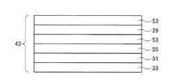
調光セル22は多層構造を有し、光学透明粘着フィルム24側から外側に向かって(すなわち光透過プレート21から離間する方向へ)、図3に示すように「保護層47、偏光層48、保護層47、粘着層46、第1電極配向層43、液晶層49、第2電極配向層44、粘着層46、位相差補償フィルム45、粘着層46、保護層47、偏光層48、保護層47、粘着層46及びハードコート層26」が層状に順次設けられている。これらの層によって、「偏光板−電極層−配向膜−液晶層−配向膜−電極層−偏光板−ハードコート層」の積層構造が作られている。
The dimming
すなわち光透過プレート21側に配置される「保護層47、偏光層48及び保護層47」によって第1偏光板41が形成され、ハードコート層26側に設けられる別の「保護層47、偏光層48及び保護層47」によって第2偏光板42が形成される。本実施形態の第1偏光板41は、光学透明粘着フィルム24を介して光透過プレート21の曲面20に貼り付けられ、第2偏光板42は、第1偏光板41よりも光透過プレート21から離間した位置に設けられる。
That is, the “
第1偏光板41及び第2偏光板42の偏光層48は、所望の偏光機能を果たす部材によって構成され、典型的には、ヨウ素化合物がドープされたPVA(ポリビニルアルコール)を延伸することによって作られる。偏光層48の典型的な配置態様として、第1偏光板41の偏光層48の吸収軸と第1偏光板41の偏光層48の吸収軸とが互いに平行である「パラレルニコル」と呼ばれる態様と、第1偏光板41の偏光層48の吸収軸と第1偏光板41の偏光層48の吸収軸とが互いに垂直である「クロスニコル(後述の図6及び図9参照)」と呼ばれる態様とがある。
The
保護層47は、隣接層を保護する役割を果たし、可視光線を透過可能な任意の材料によって構成可能であり、典型的にはTAC(トリアセチルセルロース(Triacetylcellulose))やアクリルによって構成される。なお第1偏光板41及び第2偏光板42の複数箇所に形成される保護層47は、位置に応じて異なる材料によって構成されてもよいし、同じ材料によって構成されてもよい。
The
第1偏光板41と第2偏光板42との間には、第1偏光板41側において第1電極配向層43が配置され、第2偏光板42側において第2電極配向層44が配置され、第1電極配向層43及び第2電極配向層44の各々によって「基材に支持された電極層及び配向膜」が形成される。
Between the first
図4Aは、第1電極配向層43の層構成を説明するための概略断面図である。本実施形態の第1電極配向層43は、第1偏光板41側から液晶層49側に向かって、ハードコート層53、第1樹脂基材29、ハードコート層53、インデックスマッチング層55、第1電極層31及び第1配向膜33が層状に順次設けられる。
FIG. 4A is a schematic cross-sectional view for explaining the layer configuration of the first
図4Bは、第2電極配向層44の層構成を説明するための概略断面図である。本実施形態の第2電極配向層44は、液晶層49側から第2偏光板42側に向かって、第2配向膜34、第2電極層32、インデックスマッチング層55、ハードコート層53、第2樹脂基材30及びハードコート層53が層状に順次設けられる。
FIG. 4B is a schematic cross-sectional view for explaining the layer configuration of the second
このように第1樹脂基材29と第2樹脂基材30との間には、第1樹脂基材29側に配置される第1電極層31と、第2樹脂基材30側に配置される第2電極層32とが設けられる。第1電極層31及び第2電極層32は、ITO(Indium Tin Oxide(酸化インジウムスズ))等の各種材料によって透明電極として形成可能であり、FPC(Flexible Printed Circuits)等の給電手段が接続され、電圧が印加される。第1電極層31及び第2電極層32に印加される電圧に応じて、第1電極層31と第2電極層32との間に配置される液晶層49に作用する電界が変わり、液晶層49を構成する液晶部材の配向が調整される。
As described above, between the first
第1電極層31と第2電極層32との間には、第1電極層31側に配置される第1配向膜33と、第2電極層32側に配置される第2配向膜34とが設けられる。第1配向膜33及び第2配向膜34の製法は特に限定されず、任意の手法によって液晶配向能を有する第1配向膜33及び第2配向膜34を作ることができる。例えば、ポリイミド等の樹脂層に対してラビング処理を施すことで第1配向膜33及び第2配向膜34が作られてもよいし、高分子膜に直線偏光紫外線を照射して偏光方向の高分子鎖を選択的に反応させる光配向法に基づいて第1配向膜33及び第2配向膜34が作られてもよい。
Between the
そして第1配向膜33と第2配向膜34との間には、図3に示すように、液晶層49の他にスペーサー52及びシール材36が設けられる。すなわち第1配向膜33と第2配向膜34との間には、第1配向膜33と第2配向膜34との間において液晶スペース35を区画するシール材36が設けられ、この液晶スペース35に液晶部材が充填されることで液晶層49が形成される。複数のスペーサー52は、少なくとも液晶スペース35に配置され、第1配向膜33及び第2配向膜34を支持するように離散的に配置される。各スペーサー52は、単一又は複数の部材によって構成可能であり、液晶スペース35のみにおいて積層方向へ延在してもよいし、一方の配向膜(例えば第2配向膜34)及び液晶スペース35を貫通するように積層方向へ延在してもよい。またスペーサー52はコア部と被覆部とを有し、当該被覆部が他方の配向膜(例えば第1配向膜33)と直接的に接触してもよい。したがって、例えば各スペーサー52のコア部が第2電極層32上から第2配向膜34を貫通しつつ第1配向膜33に至る直前まで液晶スペース35において延在し、第2配向膜34と同成分の被覆部がコア部上に設けられ、当該被覆部が第1配向膜33と直接的に接触することで、第1配向膜33及び第2配向膜34の間隔(セルギャップ)を各スペーサー52によって保持してもよい。
In addition to the
シール材36は、液晶層49を構成する液晶部材の漏出を防ぐ役割を果たすとともに、第1電極配向層43(第1配向膜33)と第2電極配向層44(第2配向膜34)に接着して両者を相互に固定する役割を果たす。シール材36は、一般的には熱硬化性のエポキシ樹脂が用いられ、液晶スペース35への液晶部材の充填方式が真空注入方式の場合にはエポキシ樹脂製のシール材36を好適に用いることができる。なお液晶部材の充填方式としてODF(One Drop Fill)方式が用いられる場合には、熱硬化性及びUV硬化性(紫外線硬化性)を併せ持つハブリッドタイプの材料をシール材36として好適に用いることができる。これは、液晶が未硬化のシール材36に触れることは外観上の不具合を誘発するためである。したがってシール材36を構成する材料(シール材36の組成成分)に、例えば紫外線硬化型アクリル樹脂及びエポキシ樹脂が含まれることが好ましい。また液晶部材の漏出を防ぎつつ第1電極配向層43(第1配向膜33)及び第2電極配向層44(第2配向膜34)を相互に固定する観点から、シール材36の硬さ(硬度)は、デュロメーター(JIS K6253に準拠したタイプA;10N荷重)で測定した場合の最大ポイントが20以上90以下であることが好ましく、20以上50以下であることがより好ましい。またシール材36は、ガラス転移点(ガラス転移温度(Tg))が0℃以上60℃以下であることが好ましく、0℃以上40℃以下であることがより好ましい。
The sealing
また第1電極配向層43(第1配向膜33)と第2電極配向層44(第2配向膜34)との間には、液晶層49の厚さ(すなわち第1電極配向層43(第1配向膜33)と第2電極配向層44(第2配向膜34)の間隔)を規定する複数のスペーサー52が配置される。各スペーサー52は、各種の樹脂材料によって構成可能であり、円錐台等の柱形状を有していてもよいし、球状のビーズ形状を有していてもよい。柱形状の液晶スペース35はフォトリソグラフィ技術に基づいて所望箇所に形成可能であり、またビーズ形状の液晶スペース35は予め作られて液晶スペース35に散布される。
Further, between the first electrode alignment layer 43 (first alignment film 33) and the second electrode alignment layer 44 (second alignment film 34), the thickness of the liquid crystal layer 49 (that is, the first electrode alignment layer 43 (first alignment film 43)). A plurality of spacers 52 that define a distance between the first alignment film 33) and the second electrode alignment layer 44 (second alignment film 34) are disposed. Each spacer 52 can be composed of various resin materials, and may have a columnar shape such as a truncated cone, or may have a spherical bead shape. The columnar
本実施形態の液晶層49は、「光透過プレート21に対する調光セル22の貼り合わせ性の向上(すなわち調光セル22の歪みの防止)」の観点から、液晶スペース35において陰圧を有する。例えば液晶層49を構成する液晶部材が「液晶スペース35の容積の100%未満(好ましくは99%程度)」を占めるように、液晶スペース35に液晶部材を注入することで、そのような陰圧を実現できる。本実施形態の調光セル22は曲げられた状態で光透過プレート21の曲面20に取り付けられるが、液晶スペース35に過剰な液晶部材が充填されていると調光セル22の柔軟性が損なわれて光透過プレート21に対する調光セル22の取り付け性が悪化する。したがって、液晶層49を構成する液晶部材は「液晶スペース35の容積の99%程度」を占めるように、液晶スペース35に液晶部材を注入して調光セル22の柔軟性を確保することが好ましい。なお液晶スペース35の容積に対して液晶部材の注入量が少な過ぎると、液晶スペース35内に気泡が誘発され好ましくない。
The
本実施形態の液晶層49は、VA(Vertical Alignment)方式の液晶層であり、第1電極層31及び第2電極層32に電圧が印加されていない場合に遮光状態となる「ノーマリーブラック」と呼ばれる方式を採用する。ただし液晶層49は他の駆動方式を採用してもよく、例えばTN(Twisted Nematic)方式、IPS(In Plane Switching)方式、FFS(Fringe Field Switching)方式、或いはその他の方式で液晶層49が駆動されてもよい。
The
第2偏光板42と第2電極層32(第2電極配向層44)との間には、液晶層49の駆動方式に応じた補償性能を有する位相差補償フィルム45が設けられ、本実施形態ではVA方式の液晶層49の位相差を解消するための位相差補償フィルム45が設けられる。VA方式では角度による位相差変化が大きいため、本実施形態の位相差補償フィルム45はそのような位相差変化を有効に補償できる補償性能を有する。一方、液晶層49がTN方式を採用する場合には、TN方式の液晶層49の位相差(例えば液晶分子の角度依存性)を補償するための補償性能を位相差補償フィルム45は有する。なおIPS方式の液晶層49の場合には、一般に位相差が小さく角度による位相差変化も小さいので、基本的に位相差補償フィルムを必要としないことが多く、位相差補償フィルム45が設けられなくてもよい。
Between the second
位相差補償フィルム45は、必ずしも必須な要素ではないため調光セル22に設けられなくてもよく、また所望の補償性能を発揮可能な位置であれば設置位置も限定されない。典型的には、「第1偏光板41と第1電極層31(第1電極配向層43)との間」及び「第2偏光板42と第2電極層32(第2電極配向層44)との間」のうち少なくともいずれか一方に位相差補償フィルム45が設けられる。したがって、図3に示す位置(すなわち第2電極配向層44(ハードコート層53)と第2偏光板42(保護層47)との間)ではなく、第1偏光板41(保護層47)と第1電極配向層43(ハードコート層53)との間に位相差補償フィルム45が設けられてもよい。また位相差補償フィルム45は2層以上(すなわち2箇所以上に)設けられてもよく、位相差補償フィルム45全体で、液晶層49の位相差を補償できればよい。
Since the phase
ハードコート層26は、第2偏光板42よりも光透過プレート21から離間した位置に設けられ、本実施形態の調光セル22の最外層を形成する。図示のハードコート層26は、粘着層46を介して第2偏光板42に対して固定され、任意の成分を含むことができ、例えば保護層47と同じ成分(例えばTAC等)によってハードコート層26を構成できる。なおハードコート層26は、図5に示すように第2偏光板42(本実施形態では保護層47)の表面上に直接的に形成されてもよい。例えばシリコーン系の紫外線硬化樹脂を用いて微小粒子(例えば二酸化チタン等)を含む硬化皮膜を第2偏光板42の表面上(保護層47上)に形成して、ハードコート層26として機能させてもよい。
The
そして上述の機能層(図3に示す第1偏光板41、第1電極配向層43、第2電極配向層44、位相差補償フィルム45、第2偏光板42及びハードコート層26)は、隣接機能層同士が粘着層46によって接着され、一体的な積層構造を有する。この粘着層46を構成する成分は特に限定されず、接着対象の各層の特性に応じて粘着層46の構成成分が決められてもよい。本実施形態では、全ての粘着層46が光学透明粘着フィルム(すなわちOCA)24と同じ材料によって構成されるが、紫外線硬化性樹脂等の他の成分を含む粘着層46が用いられてもよいし、配置位置や接着対象に応じて他の箇所の粘着層46とは異なる成分を含む粘着層46が用いられてもよい。
The functional layers (the first
なお図3等に示す光透過プレート21、光学透明粘着フィルム24及び調光セル22の層構成は一例に過ぎず、他の機能層が調光セル22の一部として設けられてもよいし、他の機能部が調光セル22に対して付加的に設けられてもよい。例えば図示は省略したが、調光セル22及び光学透明粘着フィルム24の側部から光透過プレート21の曲面20の一部にわたって、保護材として機能するシール保護材を設けることができる。このシール保護材によって、光透過プレート21に対する調光セル22及び光学透明粘着フィルム24の接着力を補強できるだけではなく、調光セル22及び光学透明粘着フィルム24の隣接層間の接着力も補強できる。
In addition, the layer structure of the
本件発明者は、鋭意研究の結果、曲面20(特に三次元曲面)に対して薄膜状の調光セル22を皺等の歪みなく貼り合わせるには、以下の条件を満たすように調光セル22及び光学透明粘着フィルム24を調整することが好ましいという知見を得るに至った。
As a result of earnest research, the present inventor has attached the thin-
すなわち光学透明粘着フィルム24は、光学透明粘着フィルム24及び調光セル22が積層する方向に関する厚さが、50μm以上500μm以下であり、好ましくは200μm以上300μm以下であり、室温環境での貯蔵弾性率が、1×10⁷Pa以上1×10⁸Pa以下であることがさらに好ましい。光学透明粘着フィルム24の損失正接(tanδ)は0.5以上1.5以下が好ましく、さらに好ましくは0.7以上1.2以下である。
That is, the optical transparent
光学透明粘着フィルム24は、光透過プレート21の曲面20と第1偏光板41(保護層47)とを接着する役割を果たすとともに、光透過プレート21の曲面20と第1偏光板41(保護層47)との間の曲率の相違を埋めるクッションとしての役割も果たす。したがって光学透明粘着フィルム24は、積層方向の厚さが小さ過ぎるとクッションとしての役割を適切に果たすことが難しくなる一方で、積層方向の厚さが大き過ぎると光透過プレート21の曲面に対して第1偏光板41(保護層47)を適切に固定することが難しくなる。また光学透明粘着フィルム24の貯蔵弾性率が大き過ぎると、調光セル22全体の剛性が大きくなって3次元的に形状が変化する曲面に対する追従性が不十分になる。一方、光学透明粘着フィルム24の貯蔵弾性率が小さ過ぎると、光学透明粘着フィルム24は流動性が増大し過ぎてしまい、光透過プレート21の曲面に対して第1偏光板41(保護層47)を適切に固定することが難しくなり、耐熱性等の信頼性が不十分になり通常の使用環境であっても発泡が生じる等の懸念がある。さらに光学透明粘着フィルム24の貯蔵弾性率が小さ過ぎると、光学透明粘着フィルム24の加工性が悪くなり、例えば光学透明粘着フィルム24をカットした際の糊のはみ出しに起因し、光学透明粘着フィルム24の望まれない分離が発生しうる。そのため皺等の歪みを生じさせることなく調光セル22を曲面20に対して適切に貼り合わせるには、光学透明粘着フィルム24の積層方向に関する厚さ及び貯蔵弾性率が上記範囲にあることが好ましいことを、本件発明者は新たに見出した。
The optical transparent
また第1樹脂基材29及び第2樹脂基材30は、種々の透明フィルム材によって構成可能であり、COP等の光学異方性が小さいフィルム材によって構成されることが望ましい。とりわけ調光セル22を曲面20に適切に貼り付ける観点からは、第1樹脂基材29及び第2樹脂基材30のうち少なくともいずれか一方はポリカーボネートを含むことが好ましい。なお第1樹脂基材29及び第2樹脂基材30の構成材料、形状及び/又はサイズは、相互に同じであってもよいし、異なっていてもよい。
Moreover, the 1st
またシール材36は、積層方向(第1配向膜33、シール材36及び第2配向膜34が積層する方向)に垂直な方向(すなわち幅方向)に関する長さが、1mm以上5mm以下であることが好ましく、1.5mmであることが特に好ましい。
The length of the sealing
シール材36の幅方向に関する長さが小さいほど、調光セル22全体の剛性を低下させることができ、皺等の歪みを生じさせることなく調光セル22を曲面20に貼り合わせることが容易になる。その一方で、シール材36の幅方向に関する長さが小さ過ぎると、「液晶スペース35における液晶層49の封止」や「第1電極配向層43(第1配向膜33)と第2電極配向層44(第2配向膜34)との接着」というシール材36の本来の機能が損なわれる。これらの事情を総合的に勘案すると、シール材36の幅方向の長さは上述のように好ましくは1mm以上5mm以下(より好ましくは1.5mm)であることを本件発明者は新たに見出した。
The smaller the length of the sealing
このように、概して、調光セル22を構成する積層体の剛性が小さい方が、光透過プレート21の曲面20に応じて変形しやすく、皺等の歪みを生じさせることなく調光セル22を曲面20に貼り合わせることが容易である。ただし、積層体の剛性が十分に小さいだけでは調光セル22を光透過プレート21の曲面20に適切に貼り合わせることができず、光学透明粘着フィルム24及び調光セル22には適切な条件が存在することを、本件発明者は新たに見出した。
Thus, generally, the one where the rigidity of the laminate constituting the
また調光セル22の光の透過率(特に全光線透過率)は、30%以上であることが好ましく、より好ましくは35%以上である。ここでいう「全光線透過率」は試験片の平行入射光束に対する全透過光束の割合を示し、拡散性のある試料の場合の「全透過光束」は拡散した透過光束(拡散成分)を含む。なお、全光線透過率の詳細は「JIS(Japanese Industrial Standards) 7375:2008」に基づいて定めることができる。調光セル22を透過する前の光のうち555nmの波長の光強度を基準として得られる「調光セル22を透過する光の割合」によって全光線透過率を算出することが可能である。また調光セル22の色味は、他の周辺部材との調和を考慮すると、「黒」であることが好ましいが、「黒以外の無彩色」であっても好ましい。
Further, the light transmittance (particularly the total light transmittance) of the
なお、光透過プレート21の曲面20に対する貼り合わせに起因する調光セル22の皺等の歪みは、貼り合わせ処理の始め(すなわち貼合開始領域)において特に生じやすい。当該知見に基づいて、調光装置10(光透過プレート21、光学透明粘着フィルム24及び調光セル22)において光学的な使用が本来的に意図されていない箇所やユーザーによって視認されにくい箇所を貼合開始領域として調光セル22を光透過プレート21の曲面20に貼り合わせることで、調光セル22の歪みの実質的な影響を低減できる。そのため、例えば液晶層49が設けられていないシール材36よりも外側の領域を貼合開始領域とすることで、液晶層49を通過する光に対する「調光セル22に生じる歪みによる影響」を実質的に低減できる。したがって、第1電極配向層43及び第2電極配向層44(特に第1電極層31及び第2電極層32)がシール材36の外側に延長され、この延長部にFPC等の「第1電極層31及び第2電極層32に対する給電手段」が接続される場合には、この「給電手段が接続される領域」を貼合開始領域として活用して当該領域から調光セル22を光透過プレート21の曲面20に貼り合わせることで、調光セル22に生じる歪みを効果的に隠すことができる。特に、第1電極層31及び第2電極層32の延長部分のうちFPC等の給電手段が接続される位置は、液晶層49が設けられる領域(アクティブエリア)からの距離が比較的長いため、貼合開始領域において生じる調光セル22の歪みを非アクティブエリアの範囲に収めることが容易である。
Note that distortion such as wrinkles of the
以上説明したように本実施形態に係る調光装置10によれば、光透過プレート21の曲面20に対し、光学透明粘着フィルム24を介して調光セル22を歪みなく適切に貼り合わせることができる。特に本実施形態の調光セル22によれば、偏光板(第1偏光板41及び第2偏光板42)と液晶層49の配向制御との組み合わせによって調光制御が行われるため、簡素な構成で高度な透光性能及び遮光性能を実現することができる。
As described above, according to the
また本実施形態の調光セル22は、ガラス等の硬直した要素を含まず、柔軟性に富んだ部材の組み合わせによって構成される。そのため、第1電極層31及び第2電極層32を支持する基材としてガラスを用いる場合では難しかった「曲面20に対する調光セル22の貼り合わせ」を、本実施形態の調光セル22では精度良く行うことができる。
Moreover, the
なお一般に、樹脂基材を用いた調光セルの剛性は低く、そのような低剛性の調光セルは直接的に外力が加えられると比較的簡単に変形し、液晶層の光学特性が乱される。そのため低剛性の調光セルに対して振動等の外力が突発的又は継続的に加えられる環境下で調光装置が使用されると、液晶層の液晶部材の配向が乱されて本来の光学機能を十分に発揮できず、調光装置を介して観察される光にはちらつき等の現象が生じうる。しかしながら本実施形態の調光セル22(液晶層49)は、剛性が比較的高い光透過プレート21に貼り付けられてしっかりと支持されるため、外力に起因する液晶配向の乱れを効果的に低減でき、ちらつき等の現象を回避できる。
Generally, the light control cell using a resin base material has low rigidity, and such a low rigidity light control cell is deformed relatively easily when an external force is directly applied, and the optical characteristics of the liquid crystal layer are disturbed. The Therefore, if the dimmer is used in an environment where external forces such as vibration are suddenly or continuously applied to the low-rigidity dimmer cell, the orientation of the liquid crystal member of the liquid crystal layer is disturbed and the original optical function May not be sufficiently exhibited, and a phenomenon such as flickering may occur in the light observed through the light control device. However, since the light control cell 22 (liquid crystal layer 49) of the present embodiment is attached to the
なお2枚以上のガラスプレートを有する光透過プレート21に対し調光セル22を取り付ける態様として、2枚のガラスプレートの間に調光セル22を配置する態様と、2枚のガラスプレートの外側に調光セル22を配置する態様とが考えられる。2枚のガラスプレート間に調光セル22を配置する場合、ガラスプレートによって調光セル22を保護しつつ、ガラスプレートに入射する光の透過率を調光セル22で調整することが可能である。しかしながら、2枚のガラスプレート間には比較的大きな力(圧縮力や剪断力等)が加えられることがある一方で、偏光板(第1偏光板41及び第2偏光板42)を具備する調光セル22は外側から加えられる力に対する耐性が必ずしも高くない。また使用環境によってはガラスプレート間の温度が非常に高くなるが、偏光板は必ずしも高温耐性に優れていない。したがって偏光板を具備する調光セル22を2枚のガラスプレート間に配置する場合には、調光セル22が潰されたり劣化したりして、所望の調光機能を調光セル22が果たせなくなる懸念がある。
In addition, as an aspect which attaches the
一方、図1及び図3等に示す本実施形態の調光装置10のように、光透過プレート21の外面に調光セル22を取り付ける態様では、調光セル22に要求される耐力性能及び耐温性能は高くない。したがって本実施形態の調光装置10は、調光セル22が偏光板(第1偏光板41及び第2偏光板42)を具備しているにもかかわらず、所望の調光機能を継続的に発揮することができる。また、皺等の歪みを生じさせることなく調光セル22を曲面20に貼り合わせることを容易にする上述の条件を満たす調光セル22を使うことで、調光セル22の透光性能及び遮光性能を過度に損なうことなく、様々な形状を持ちうる曲面20の具体的な曲がり具合に応じて、調光セル22を光透過プレート21に対して適切に貼り合わせることができる。
On the other hand, in a mode in which the
<VA方式に関する偏光板の吸収軸と基材の光軸との方向性>
液晶層49の駆動方式がVA方式の場合、「第1偏光板41及び第2偏光板42の偏光層48の吸収軸の方向」及び「第1電極配向層43及び第2電極配向層44の基材(第1樹脂基材29及び第2樹脂基材30)の光軸の方向」に関して、以下の関係性がある。
<Directivity between absorption axis of polarizing plate and optical axis of substrate for VA system>
When the driving method of the
<第1の配置態様>
図6は、第1の配置態様を説明するための第1樹脂基材29、第2樹脂基材30、第1偏光板41の偏光層48及び第2偏光板42の偏光層48を示す図である。
<First Arrangement Mode>
FIG. 6 is a diagram showing a first
本態様では、第1樹脂基材29の光軸は第2樹脂基材30の光軸に垂直であり(図6の光軸方向「Db1」、「Db2」参照)、第1偏光板41の偏光層48の吸収軸は第2偏光板42の偏光層48の吸収軸に垂直であり(図6の吸収軸方向「Da1」、「Da2」参照)、第1樹脂基材29の光軸方向Db1は第1偏光板41の偏光層48の吸収軸方向Da1と平行であり、第2樹脂基材30の光軸方向Db2は第2偏光板42の偏光層48の吸収軸方向Da2と平行である。
In this aspect, the optical axis of the first
上述のように「第1樹脂基材29の光軸方向Db1が第2樹脂基材30の光軸方向Db2に垂直である」ように第1樹脂基材29及び第2樹脂基材30を配置することで、透過光に対して第1樹脂基材29により付与される位相差を、第2樹脂基材30により付与される位相差によってキャンセルできる。したがって透過光に対して第1樹脂基材29及び第2樹脂基材30により付与される位相差を、全体として低減することができる。
As described above, the first
また「第1樹脂基材29の光軸方向Db1と第1偏光板41の偏光層48の吸収軸方向Da1とが平行」となるように、また「第2樹脂基材30の光軸方向Db2と第2偏光板42の偏光層48の吸収軸方向Da2とが平行」となるように第1樹脂基材29、第2樹脂基材30、第1偏光板41及び第2偏光板42を配置することで、第1樹脂基材29及び第2樹脂基材30の光学異方性に起因する「遮光時(すなわち黒表示時)の視野角特性の悪化や遮光率の悪化」を抑えることができる。すなわち、本来的に光学異方性を有する樹脂基材(第1樹脂基材29及び第2樹脂基材30)は透過光に影響を与え、特にVA方式の液晶層49を備える調光セル22(調光装置10)では、遮光時の視野角や遮光率を悪化させる。一方、本実施形態のように「積層方向に関して液晶層49の前後に配置される第1樹脂基材29及び第2樹脂基材30の光軸方向Db1、Db2が互いに垂直であり」且つ「液晶層49を介して同じ側に配置される基材の光軸方向及び偏光板の吸収軸方向(すなわち「第1樹脂基材29の光軸方向Db1及び第1偏光板41の偏光層48の吸収軸方向Da1」及び「第2樹脂基材30の光軸方向Db2及び第2偏光板42の偏光層48の吸収軸方向Da2」)を平行にする」ことで、遮光時の視野角や遮光率の悪化を抑えることができる。
Further, “the optical axis direction Db1 of the first
図7は、第1の配置態様に対する比較態様を示す第1樹脂基材29、第2樹脂基材30、第1偏光板41の偏光層48及び第2偏光板42の偏光層48を示す図である。図7に示す比較態様では、第1樹脂基材29の光軸方向Db1が第2樹脂基材30の光軸方向Db2に垂直であり、第1偏光板41の偏光層48の吸収軸方向Da1が第2偏光板42の偏光層48の吸収軸方向Da2に垂直であり、第1樹脂基材29の光軸方向Db1が第1偏光板41の偏光層48の吸収軸方向Da1に垂直であり、第2樹脂基材30の光軸方向Db2が第2偏光板42の偏光層48の吸収軸方向Da2に垂直である。
FIG. 7 is a diagram showing the first
図8は、図6に示す第1の配置態様に関する調光セル22の視野角特性(図8の符号「L1」参照)と、図7に示す比較態様に関する調光セル22の視野角特性(図8の符号「L2」参照)とを示す。なお図8に示す視野角特性L1、L2は、図1、図3、図4A及び図4Bに示す構成を有する調光装置10を使って、遮光状態(すなわち電源OFF状態)で、極角を60度として方位角を変化させながら透過率を計測することで得られた。図8の横軸は方位角(°)を示し、縦軸は拡散成分も含む全光線透過率(%)を示す。なお図8に示す「方位角=0°」は、第1偏光板41の偏光層48の吸収軸方向Da1の一方側に対応する。
8 is a view angle characteristic of the dimming
また、ここでいう「全光線透過率」は試験片の平行入射光束に対する全透過光束の割合を示し、拡散性のある試料の場合の「全透過光束」は拡散した透過光束(拡散成分)を含む。なお、全光線透過率の詳細は「JIS(Japanese Industrial Standards) 7375:2008」に基づいて定めることができる。全光線透過率の測定には光源として「ダイクロミラー付ハロゲンランプ」を使用した。測定対象の調光セル22を透過する前の光のうち555nmの波長の光強度を基準として得られる「調光セル22を透過する光の割合」によって全光線透過率が算出される。したがって調光セル22を透過する前の555nm波長の光強度を「100(%)」で表した場合の、調光セル22を透過した後の可視光波長の光強度の値(%)によって全光線透過率を表すことができる。測定に使用した調光セル22の厚さは約0.55mmであり、測定装置として村上色彩技術研究所のヘイズメーターHM−150を用いた。
The “total light transmittance” here indicates the ratio of the total transmitted light beam to the parallel incident light beam of the test piece, and the “total transmitted light beam” in the case of a diffusible sample indicates the diffused transmitted light beam (diffuse component). Including. The details of the total light transmittance can be determined based on “JIS (Japan Industrial Standards) 7375: 2008”. A “halogen lamp with a dichroic mirror” was used as a light source for measuring the total light transmittance. The total light transmittance is calculated by “the ratio of the light that passes through the
図8からも明らかなように、図6に示す第1の配置態様(図8の符号「L1」参照)によれば、図7に示す比較態様(図8の符号「L2」参照)に比べ、方位角の変化に伴う透過率の変動量を低減することができ、視野角特性に優れた調光セル22(調光装置10)を提供できることが分かる。 As is clear from FIG. 8, the first arrangement mode shown in FIG. 6 (see the reference symbol “L1” in FIG. 8) is compared with the comparison mode shown in FIG. 7 (see the reference symbol “L2” in FIG. 8). Thus, it can be seen that the amount of variation in the transmittance with the change in the azimuth angle can be reduced, and the dimming cell 22 (the dimming device 10) having excellent viewing angle characteristics can be provided.
また透過率(全光線透過率)の大きさ自体に関しても、第1の配置態様に係る調光セル22の透過率L1の方が比較態様に係る調光セル22の透過率L2よりも全体的に小さく抑えられており、第1の配置態様に係る調光セル22が優れた遮光性能を発揮しうることが分かる。
Further, with regard to the magnitude of the transmittance (total light transmittance) itself, the transmittance L1 of the dimming
<第2の配置態様>
図9は、第2の配置態様を説明するための第1樹脂基材29、第2樹脂基材30、第1偏光板41の偏光層48、第2偏光板42の偏光層48、及び位相差補償フィルム45aを示す図である。
<Second Arrangement Mode>
FIG. 9 shows the first
本態様では、第1偏光板41と第1電極配向層43との間に位相差補償フィルム45aが設けられている。この位相差補償フィルム45aは、粘着層(OCA)46を介して第1偏光板41(保護層47)に接着されるとともに、他の粘着層(OCA)46を介して第1電極配向層43(ハードコート層53(図4A参照))に接着され、Aプレートとして機能する。Aプレートとして機能する位相差補償フィルム45aでは、フィルム面内のx方向の屈折率(nx)が、当該x方向と垂直なy方向の屈折率(ny)よりも大きく、x方向及びy方向と垂直なz方向の屈折率(nz)がy方向の屈折率(ny)と等しくなる(すなわち「nx>ny=nz」の関係が満たされる)。位相差補償フィルム45aを構成する材料は特に限定されないが、本実施形態の位相差補償フィルム45aは、COPによって作られる2軸延伸透明フィルムによって構成される。
In this embodiment, a
そして第1樹脂基材29の光軸は第2樹脂基材30の光軸と平行であり(図9の光軸方向「Db1」、「Db2」参照)、第1偏光板41の偏光層48の吸収軸は第2偏光板42の偏光層48の吸収軸に垂直であり(図9の吸収軸方向「Da1」、「Da2」参照)、第1樹脂基材29の光軸方向Db1は第1偏光板41の偏光層48の吸収軸の方向Da1に垂直であり、第2樹脂基材30の光軸方向Db2は第2偏光板42の偏光層48の吸収軸の方向Da2と平行である。
The optical axis of the first
上述のように、「第1樹脂基材29の光軸方向Db1と第2樹脂基材30の光軸方向Db2とが平行となる(一致する)」ように第1樹脂基材29及び第2樹脂基材30を配置することで、第1樹脂基材29及び第2樹脂基材30をそれぞれロールから繰り出しながら連続的に供給することができる。一般に第1樹脂基材29及び第2樹脂基材30は、ロール状態に形成され、そのロールから順次繰り出され、各調光セル22に応じた形状及びサイズに切り出されて使われる。その一方で、樹脂製の基材には製造過程の延伸処理によって延伸方向が光軸の方向となるような光学異方性がもたらされ、ロールの状態では長手方向(すなわち繰り出し方向)が光軸の方向となるのが一般的である。そのため本配置態様のように「第1樹脂基材29の光軸方向Db1と第2樹脂基材30の光軸方向Db2とが一致する場合」には、ロールから繰り出される第1樹脂基材29とロールから繰り出される第2樹脂基材30とを、方向を調整することなく、繰り出しながら連続的に重ね合わせることができる。したがって例えば、ロールから繰り出された第1樹脂基材29及び第2樹脂基材30の上に図4A及び図4Bに示すようなハードコート層53、インデックスマッチング層55、第1電極層31、第2電極層32、第1配向膜33及び第2配向膜34を配設することで、長尺の第1電極配向層43及び第2電極配向層44を作製することができ、大面積の調光セル22を効率良く量産することができる。
As described above, the first
なお「第1樹脂基材29の光軸方向Db1と第2樹脂基材30の光軸方向Db2とが平行となる(一致する)」ように第1樹脂基材29及び第2樹脂基材30を配置する場合には、第1樹脂基材29及び第2樹脂基材30の光学異方性が調光セル22の透過光に強く影響し、例えば遮光時(すなわち黒表示時)に視野角特性や遮光率を悪化させることがある。このような視野角特性及び遮光率の悪化を抑えるために、本配置態様では、第2樹脂基材30の光軸方向Db2と第2偏光板42の偏光層48の吸収軸方向Da2とが平行になるように、第2樹脂基材30及び第2偏光板42の偏光層48は配置される。また位相差補償フィルム45aの遅相軸方向Dcと第2樹脂基材30の光軸方向Db2とが平行になるように、位相差補償フィルム45a及び第2樹脂基材30は配置される。また第1偏光板41の偏光層48の吸収軸方向Da1が第2偏光板42の偏光層48の吸収軸方向Da2に垂直であるように、第1偏光板41の偏光層48及び第2偏光板42の偏光層48は配置される。これにより、第1樹脂基材29及び第2樹脂基材30の光学異方性に起因する「遮光時(すなわち黒表示時)の視野角特性の悪化や遮光率の悪化」を抑えることができる。
The first
なお図9に示す第2の配置態様の一変形例として、第1樹脂基材29と第1偏光板41の偏光層48との間ではなく、第2樹脂基材30と第2偏光板42の偏光層48との間にAプレートとして機能する位相差補償フィルム45aが設けられてもよい。この場合、 位相差補償フィルム45aの遅相軸方向Dcが、第1樹脂基材29の光軸方向Db1、第2樹脂基材30の光軸方向Db2及び第1偏光板41の偏光層48の吸収軸方向Da1と平行となるように、各部材が配置される。このような配置によっても、第1樹脂基材29及び第2樹脂基材30の光学異方性に起因する「遮光時(すなわち黒表示時)の視野角特性の悪化や遮光率の悪化」を抑えることができる。
As a modification of the second arrangement mode shown in FIG. 9, the second
図10は、第2の配置態様に対する比較態様を示す第1樹脂基材29、第2樹脂基材30、第1偏光板41の偏光層48、第2偏光板42の偏光層48、及び位相差補償フィルム45aを示す図である。図10に示す比較態様では、第1樹脂基材29の光軸方向Db1は第2樹脂基材30の光軸方向Db2と平行であり、第1偏光板41の偏光層48の吸収軸方向Da1は第2偏光板42の偏光層48の吸収軸方向Da2に垂直であるが、第1樹脂基材29の光軸方向Db1は第1偏光板41の偏光層48の吸収軸の方向Da1と平行であり、第2樹脂基材30の光軸方向Db2は第2偏光板42の偏光層48の吸収軸の方向Da2に垂直である。
FIG. 10 shows the first
図11は、図9に示す第2の配置態様に関する調光セル22の視野角特性(図11の符号「L3」参照)と、図10に示す比較態様に関する調光セル22の視野角特性(図11の符号「L4」参照)とを示す。なお図11に示す視野角特性L3、L4は、図1、図3、図4A及び図4Bに示す構成において位相差補償フィルム45(図3参照)の代わりに位相差補償フィルム45a(図9及び図10参照)が配置された調光装置10が使われ、遮光状態(すなわち電源OFF状態)で、極角を60度として方位角を変化させながら透過率を計測することで得られた。図11の横軸は方位角(°)を示し、縦軸は拡散成分も含む全光線透過率(%)を示す。なお図11に示す「方位角=0°」は、第1偏光板41の偏光層48の吸収軸方向Da1の一方側に対応する。また全光線透過率は、上述の図8に示す場合と同様にして測定された。
11 shows the viewing angle characteristics of the dimming
図11からも明らかなように、図9に示す第2の配置態様(図11の符号「L3」参照)によれば、図10に示す比較態様(図11の符号「L4」参照)に比べ、方位角の変化に伴う透過率の変動量を低減することができ、視野角特性に優れた調光セル22(調光装置10)を提供できることが分かる。 As is clear from FIG. 11, the second arrangement mode shown in FIG. 9 (see “L3” in FIG. 11) compares with the comparative mode shown in FIG. 10 (see “L4” in FIG. 11). Thus, it can be seen that the amount of variation in the transmittance with the change in the azimuth angle can be reduced, and the dimming cell 22 (the dimming device 10) having excellent viewing angle characteristics can be provided.
また透過率(全光線透過率)の大きさ自体に関しても、第2の配置態様に係る調光セル22の透過率L3の方が比較態様に係る調光セル22の透過率L4よりも全体的に小さく抑えられており、第2の配置態様に係る調光セル22が優れた遮光性能を発揮しうることが分かる。
Further, regarding the size of the transmittance (total light transmittance) itself, the transmittance L3 of the
<実施例>
次に、光透過プレート21に対する調光セル22の貼り合わせ性能の検証結果に関する各種の実施例ついて説明する。
<Example>
Next, various examples relating to the verification results of the bonding performance of the
図12は、光透過プレート21の曲面20に対する調光セル22(実施例1〜3)の貼り合わせの状態評価を示す表である。
FIG. 12 is a table showing a state evaluation of bonding of the light control cell 22 (Examples 1 to 3) to the
実施例1及び実施例3の調光装置10では、同じ調光セル22が使用されているが、光透過プレート21の平面サイズ(積層方向に垂直な方向のX方向サイズ及びY方向サイズ)、厚さ(積層方向の長さ(Z方向サイズ))及び光透過プレート21の曲面20の曲率が異なっている。なお図12の「1800R」は半径1800mmの円が描くカーブの曲率を示し、「1400R」は半径1400mmの円が描くカーブの曲率を示す。
In the
実施例1及び実施例3の調光装置10で使用されている調光セル22は、平面サイズ(積層方向に垂直な方向のX方向サイズ及びY方向サイズ)が280mm(X方向サイズ)及び288mm(Y方向サイズ)であり、厚さ(積層方向の長さ(Z方向サイズ))が0.63mmであり、基材(図3の第1樹脂基材29及び第2樹脂基材30参照)としてポリカーボネートが使用され、電極基材としてこのポリカーボネート基材を用いたITOフィルムが用いられ、偏光層(図3の偏光層48参照)として液晶ディスプレー(LCD)及びカーナビゲーション用途で実績のある染料系及びヨウ素系の偏光素子が用いられ、液晶層49に設けられるスペーサー(図3のスペーサー52参照)として6μmの直径を持ちランダムに配置された多数のビーズ状スペーサーが用いられ、UV硬化性樹脂及び熱硬化性樹脂を含むハイブリッドシール材36であって幅方向の長さ(積層方向に垂直な方向の長さ)が1.5mmのシール材36が用いられた。
The dimming
一方、実施例2の調光装置10では、実施例3と同じ光透過プレート21が用いられ、平面サイズ(積層方向に垂直な方向のX方向サイズ及びY方向サイズ)が423mm(X方向サイズ)及び337mm(Y方向サイズ)であり、厚さ(積層方向の長さ(Z方向サイズ))が0.7mmであった。また実施例2の調光装置10で使用されている調光セル22は、平面サイズ(積層方向に垂直な方向のX方向サイズ及びY方向サイズ)が280mm(X方向サイズ)及び280mm(Y方向サイズ)であり、厚さ(積層方向の長さ(Z方向サイズ))が0.54mmであり、基材(図3の第1樹脂基材29及び第2樹脂基材30参照)としてCOPが使用され、偏光板(図3の偏光層48参照)の光学補償フィルムとしてVA補償用のCOP2軸プレートが用いられ、液晶層49に設けられるスペーサー(図3のスペーサー52参照)として15μmの断面径を有し230μmピッチで離間する複数の柱状スペーサーが用いられ、幅方向の長さ(積層方向に垂直な方向の長さ)が5mmのシール材36が用いられた。実施例2の調光セル22の他の構成は、上述の実施例1及び3の調光セル22と同じであった。
On the other hand, in the
実施例1〜3に係る調光装置10の他の構成は、図3に示す構成と同様であった。
The other structure of the
上述の実施例1〜3の調光装置10において、光透過プレート21に対する調光セル22の貼り合わせ状態を目視により確認したところ、実施例1及び実施例3の調光セル22では目立った歪み(皺等)は発生していなかったのに対し、実施例2の調光セル22では皺が目立ち光透過プレート21に対して調光セル22を適切に貼り合わせることができなかった。
In the
図13は、光透過プレート21の曲面20に対する調光セル22(実施例4〜9)の貼り合わせの状態評価を示す表である。
FIG. 13 is a table showing a state evaluation of bonding of the light control cell 22 (Examples 4 to 9) to the
実施例4〜9では、「同じ特性を有する光透過プレート21」に対して「同じ特性を有する光学透明粘着フィルム24」を介して「異なる特性を有する調光セル22」を貼り付けて、光透過プレート21に貼り付けられた調光セル22の状態を評価した。具体的には、光透過プレート21は、平面サイズが423mm(X方向長さ)及び337mm(Y方向長さ)であり、厚さ(Z方向長さ)が0.7mmであった。
In Examples 4 to 9, “
調光セル22は、主に、基材(図4Aの第1樹脂基材29及び図4Bの第2樹脂基材30参照)、スペーサー52の形状、シール材36の幅方向の長さ(図13の「シール幅」参照)、第1偏光板41(特に図3の「偏光層48」参照)及び第2偏光板42(特に図3の「偏光層48」参照)を図13に示すように適宜変えた。
The dimming
図13の「基材」の項目は、実際に用いられた基材の成分を表し、COP(実施例4、6及び7)又はポリカーボネート(実施例5及び8〜9)が用いられた。 The item “substrate” in FIG. 13 represents the components of the substrate actually used, and COP (Examples 4, 6 and 7) or polycarbonate (Examples 5 and 8 to 9) was used.
図13の「スペーサー」の項目において、「柱状」は15μmの断面径を有する円柱状の複数のスペーサー52が230μmピッチで離間して配置されていることを示し、「ビーズ状」は6μmの直径を持つ球状の複数のスペーサー52がランダムに配置されていることを示す。 In the item of “spacer” in FIG. 13, “columnar” indicates that a plurality of cylindrical spacers 52 having a cross-sectional diameter of 15 μm are spaced apart at a pitch of 230 μm, and “bead-shaped” indicates a diameter of 6 μm. It shows that a plurality of spherical spacers 52 having the following are arranged at random.
図13の「シール幅」において、「5mm(+余白5mm)」は、積層方向に垂直な方向に関するシール材36の長さが5mmであって、シール材36を介して液晶層49と反対側において、積層方向に垂直な方向に関し、第1電極配向層43及び第2電極配向層44が5mmだけ突出している状態を示す。また「1.5mm(+余白0mm)」は、積層方向に垂直な方向に関するシール材36の長さが1.5mmであって、シール材36を介して液晶層49と反対側において、積層方向に垂直な方向に関し、第1電極配向層43及び第2電極配向層44が0mmだけ突出している(すなわち第1電極配向層43及び第2電極配向層44がシール材36から突出していない)状態を示す。
In the “seal width” of FIG. 13, “5 mm (+ margin 5 mm)” indicates that the length of the sealing
図13の「第1偏光板」は第1偏光板41の偏光層48の部材を示し、「第2偏光板」は第2偏光板42の偏光層48の部材を示す。図13の「ヨウ素系(COP2軸補償板付)」はヨウ素系の偏光子であって2軸性の光学補償性能を有するCOP製の板が取り付けられた偏光子によって偏光層48が構成されていることを示し、「ヨウ素系」はヨウ素系の偏光子(光学補償板無し)によって偏光層48が構成されていることを示し、「染料系」は染料系の偏光子(光学補償板無し)によって偏光層48が構成されていることを示す。
In FIG. 13, “first polarizing plate” indicates a member of the
図13の「貼合状態」は光学透明粘着フィルム24を介して光透過プレート21の曲面20に貼り合わされた調光セル22の状態(特に皺等の歪みの程度及び有無)を示す。「Very Bad」(実施例4)は、調光セル22に非常に目立つ皺が発生し、調光セル22にはトンネリングと呼ばれる筒状の皺部分が形成され、調光セル22が実用上使えない状態にあることを示す。「Bad」(実施例5)は、調光セル22に目立つ皺が発生し、調光セル22にはトンネリングが形成され、調光セル22が実用上の使用が容易ではない状態にあることを示す。「Average」(実施例6)は、調光セル22に生じた皺は目立たないが、調光セル22には小さなトンネリングが形成されたことを示す。「Good」(実施例7)は、調光セル22には目立たない皺が僅かに生じたがトンネリングは形成されず、調光セル22が実用可能な状態にあることを示す。「Excellent」(実施例8〜9)は、調光セル22において皺等の歪みは確認されず、非常に良好な状態で調光セル22が光透過プレート21に貼り付けられており、調光セル22が良好な透光性能及び遮光性能を発揮する状態にあることを示す。
The “bonding state” in FIG. 13 indicates the state of the
実施例4〜9に係る調光装置10の他の構成は、図3に示す構成と同様であった。
The other configuration of the
図13に示す結果からは、実施例4の調光装置10に比べ、実施例5〜7の調光装置10では調光セル22の貼合状態が改善されていることが分かる。実施例5の調光セル22は、基材(図4Aの第1樹脂基材29及び図4Bの第2樹脂基材30参照)としてCOPではなくポリカーボネートが用いられている点以外は、実施例4の調光セル22と同じ構成を有する。したがって第1樹脂基材29及び第2樹脂基材30の構成材料としてポリカーボネートが好ましいことが分かる。また実施例6の調光セル22は、第1偏光板41及び第2偏光板42の偏光層48として「2軸性光学補償性能を有するCOP製の板が取り付けられたヨウ素系偏光子」や「ヨウ素系偏光子」ではなく「染料系偏光子」が用いられている点以外は、実施例4の調光セル22と同じ構成を有する。したがって第1偏光板41及び第2偏光板42の偏光層48の構成材料として染料系偏光子が好ましいことが分かる。また実施例7の調光セル22は、シール材36の幅が1.5mmであり且つ第1電極配向層43及び第2電極配向層44の延長部分がない(すなわち「余白=0mm」)点以外は、実施例4の調光セル22と同じ構成を有する。したがって積層方向に垂直な方向に関するシール材36の幅は1.5mmが好ましいことが分かる。なお、シール材36の幅が細過ぎると、シール材36の密着力の低下に起因して調光セル22の決壊が生じることがある。一方、シール材36の幅が太すぎると、3次元的に形状が変化する曲面に対するシール材36の追従性が不十分になる可能性がある。
From the results shown in FIG. 13, it can be seen that the bonding state of the
また図13に示す実施例8〜9の調光セル22では、「第1樹脂基材29及び第2樹脂基材30の構成材料としてポリカーボネートが用いられ(実施例5参照)」、「第1偏光板41及び第2偏光板42の偏光層48の構成材料として染料系偏光子が用いられ(実施例6参照)」、及び「シール材36の幅が1.5mmであり且つ第1電極配向層43及び第2電極配向層44の延長部分がない(実施例7参照)」点以外は、実施例4の調光セル22と同じ構成を有する。実施例8〜9に係る調光セル22の貼合状態が実施例4〜7に係る調光セル22よりも良好な状態であったことからも、上述の実施例4〜7の考察が適切であることが推認される。
In the
なお実施例8の調光セル22と実施例9の調光セル22とは、スペーサー52の形状が異なる点以外は同じ構成を有するが、実施例8の調光セル22及び実施例9の調光セル22の貼合状態はいずれも非常に良好であった。したがってスペーサー52の形状が調光セル22の貼合状態に及ぼす影響は全くないか若しくは非常に小さいことが推認される。
The
図14は、光透過プレート21の曲面20に対する調光セル22(実施例10〜12)の貼り合わせの状態評価を示す表である。
FIG. 14 is a table showing a state evaluation of bonding of the light control cell 22 (Examples 10 to 12) to the
実施例10〜12では、「同じ特性を有する光透過プレート21」に対して「異なる特性を有する光学透明粘着フィルム24」を介して「同じ特性を有する調光セル22」を貼り付けて、光透過プレート21に貼り付けられた調光セル22の状態を評価した。具体的には、上述の実施例8(図13)と同じ特性の光透過プレート21及び調光セル22を使用する一方で、積層方向に関する厚さ、室温での貯蔵弾性率及び損失正接が異なる光学透明粘着フィルム24を使用した。図14に示す実施例10〜12のこれらの物性は、振動数を10Hz(ヘルツ)に設定し、昇温条件を5℃/min(分)に設定し、株式会社UBM(ユービーエム)性の測定器「Rheogel E4000」を用いて測定して得られた値である。図14には、25℃及び50℃の各々の場合における貯蔵弾性率及び損失正接が示されている。
In Examples 10 to 12, the “
図14の「調光セルの貼合状態」の項目に関し、「Average」(実施例10)は調光セル22に多少の歪みが見られた状態を示す。「Good」(実施例11)は、実施例10の調光セル22の歪みよりも小さい歪みが調光セル22に見られたが、調光セル22が比較的良好な状態にあることを示す。「Excellent」(実施例12)は、調光セル22には歪みが全く見られず、調光セル22が非常に良好な状態にあることを示す。
With regard to the item of “bonding state of light control cell” in FIG. 14, “Average” (Example 10) indicates a state in which some distortion is observed in the
実施例10〜12を比較考量すると、光透過プレート21に対する調光セル22の貼合状態を改善する観点からは、光学透明粘着フィルム24の貯蔵弾性率は小さい方が好ましい(例えば実施例10(「2.9×10⁷Pa/25℃」)及び実施例11(「1.1×107Pa/25℃」)参照)ことが分かる。さらに光学透明粘着フィルム24の損失正接は小さい方が好ましい(例えば実施例10(「0.95/25℃」)、実施例11(「0.90/25℃」)参照)及び実施例12(「0.41/25℃」)ことが分かる。また積層方向に関する光学透明粘着フィルム24の厚さは厚い方が好ましいと考えられるが、実施例10〜12を比較考量すると光学透明粘着フィルム24の厚さよりも光学透明粘着フィルム24の貯蔵弾性率と損失正接の方が、光透過プレート21に対する調光セル22の貼合状態に与える影響が大きいと考えられる。
From the viewpoint of improving the bonding state of the
<スペーサーの詳細構成>
以下、「スペーサー52の硬度」と「スペーサー52の先端が当接する部位の硬度」との好ましい関係例について説明する。
<Detailed configuration of spacer>
Hereinafter, an example of a preferable relationship between “the hardness of the spacer 52” and “the hardness of the portion where the tip of the spacer 52 abuts” will be described.
以下で説明する実施形態では、図15に示す調光セル22の製造工程によりフォトレジストを使用して円柱形状又は円錐台形状によりスペーサー52が形成される。すなわち調光セル22の製造工程では、第1の積層体の製造(図15の符号「SP1」参照)、第2の積層体の製造(図15の符号「SP2」参照)、液晶セル(図3の「液晶層49」参照)の製造(図15の符号「SP3」参照)、及びこれらの部材の積層(図15の符号「SP4」参照)が順次行われる。なお第1の積層体の製造工程SP1には、電極(すなわち「第2電極層32」)の製造工程SP1−1、スペーサー52の製造工程SP1−2及び配向層(すなわち「第2配向膜34」)の製造工程SP1−3が含まれる。また図示は省略したが、第2の積層体の製造工程SP2には、電極(すなわち第1電極層31)の製造工程及び配向層(すなわち「第1配向膜33」)の製造工程が含まれる。このようにしてスペーサー52を製造して、この実施形態では、各スペーサー52のビッカース硬度値Xsが16.9以上40.2以下であり(すなわち「16.9≦Xs≦40.2」が満たされ)、スペーサー52の先端が当接する第1電極配向層43(特に第1配向膜33)の部位のビッカース硬度値Xfが、11.8以上35.9以下であるように設定され(すなわち「11.8≦Xf≦35.9」が満たされ)、これによりスペーサーに関する信頼性を従来に比して一段と向上する。なお、ビッカース硬度の値は、以下の実施例に記載の条件における測定値である。
In the embodiment described below, the spacer 52 is formed in a columnar shape or a truncated cone shape using a photoresist by the manufacturing process of the
例えば、被覆部が設けられず主としてコア部のみによって各スペーサー52が構成されている場合(すなわちスペーサー52がコア部を含むが被覆部を含まない場合)には、複数のスペーサー(コア部)52の各々のビッカース硬度値によって上記のXsが表され、複数のスペーサー52の各々の先端が当接する第1配向膜33の部位のビッカース硬度値によって上記のXfが表される。一方、コア部上に被覆部が設けられて主としてコア部及び被覆部の組み合わせによって各スペーサー52が構成されている場合(すなわちスペーサー52がコア部及び被覆部を含む場合)には、各スペーサー52のコア部及び被覆部のビッカース硬度値によって上記のXsが表され、複数のスペーサー52の各々の先端を被覆する被覆部が当接する第1配向膜33の部位のビッカース硬度値によって上記のXfが表される。ここで言う「各スペーサー52のコア部及び被覆部のビッカース硬度値」は、コア部が被覆部によって被覆された状態で計測されるビッカース硬度値を意味する。
For example, in the case where each spacer 52 is configured only by the core portion without the covering portion (that is, when the spacer 52 includes the core portion but does not include the covering portion), a plurality of spacers (core portions) 52 are provided. The above Xs is represented by each Vickers hardness value, and the above Xf is represented by the Vickers hardness value of the portion of the
スペーサー52の先端が当接する第1電極配向層43(特に第1配向膜33)の部位のビッカース硬度値Xfが11.8未満の場合、使用中の押圧力により、スペーサー52の先端が対向する面に貫入し、その結果、セルギャップが不均一化したり、局所的な配向不良が発生する。またこの場合、スペーサー52の組み立て時の接触等により第1樹脂基材29にキズが発生したり、全体を屈曲した際にクラックが生じたりする。
When the Vickers hardness value Xf of the portion of the first electrode alignment layer 43 (particularly the first alignment film 33) with which the tip of the spacer 52 abuts is less than 11.8, the tip of the spacer 52 faces due to the pressing force during use. As a result, the cell gap becomes non-uniform or local alignment failure occurs. Further, in this case, the first
またスペーサー52のビッカース硬度値Xsが16.9未満の場合には、外圧によりスペーサー52が潰れてセルギャップが低減し、所望のセルギャップを得られなくなる。またスペーサー52のビッカース硬度値Xsが40.2を超える場合、又はスペーサー52の先端が当接する第1電極配向層43(特に第1配向膜33)の部位のビッカース硬度値Xfが35.9を超える場合にあっても、セルギャップが低減したり、キズやクラックが発生したりする場合がある。 When the Vickers hardness value Xs of the spacer 52 is less than 16.9, the spacer 52 is crushed by the external pressure, the cell gap is reduced, and a desired cell gap cannot be obtained. Further, when the Vickers hardness value Xs of the spacer 52 exceeds 40.2, or the Vickers hardness value Xf of the portion of the first electrode alignment layer 43 (particularly the first alignment film 33) with which the tip of the spacer 52 abuts is 35.9. Even if it exceeds, the cell gap may be reduced or scratches or cracks may occur.
しかしながらスペーサー52のビッカース硬度値Xsが16.9以上40.2以下であり、スペーサー52の先端が当接する第1電極配向層43(特に第1配向膜33)の部位のビッカース硬度値Xfが、11.8以上35.9以下であるように設定すれば、これらの問題を一挙に解決してスペーサー52に関する信頼性を従来に比して一段と向上することができる。 However, the Vickers hardness value Xs of the spacer 52 is 16.9 or more and 40.2 or less, and the Vickers hardness value Xf of the first electrode alignment layer 43 (particularly the first alignment film 33) with which the tip of the spacer 52 abuts is If it is set to be 11.8 or more and 35.9 or less, these problems can be solved at once, and the reliability related to the spacer 52 can be further improved as compared with the related art.
〔試験結果〕
図16及び図17は、このスペーサーに関する構成の確認に供した試験結果を示す図表である。図16及び図17における実施例は、スペーサー52及びこのスペーサー52が当接する配向層に関する構成が異なる点を除いて、同一に構成される。より具体的には、これらの実施例の調光セルは、下側積層体(第2電極配向層44参照)にのみスペーサー52を設けるようにし、このスペーサー52に係る製造条件を調整することにより、スペーサー52のビッカース硬度値Xsを変化させた。また第1配向膜33を製造する際の条件を調整することにより、スペーサー52の先端が当接する第1電極配向層43(特に第1配向膜33)の部位のビッカース硬度値Xfを変化させた。
〔Test results〕
FIG. 16 and FIG. 17 are charts showing test results used for confirming the configuration related to this spacer. The embodiment in FIGS. 16 and 17 has the same configuration except that the configuration regarding the spacer 52 and the alignment layer with which the spacer 52 abuts is different. More specifically, in the light control cells of these examples, the spacer 52 is provided only in the lower laminate (see the second electrode alignment layer 44), and the manufacturing conditions relating to the spacer 52 are adjusted. The Vickers hardness value Xs of the spacer 52 was changed. Further, by adjusting the conditions for manufacturing the
すなわちスペーサー52は、スペーサー52に係る塗工液を塗工した後、乾燥させ、その後、露光装置を使用したマスク露光により、スペーサー52を製造する部位を選択的に露光する。なおこれはネガ型のフォトレジストの場合であり、ポジ型のフォトレジストではこれとは逆にスペーサー52を配設する部位を除く部位が選択的に露光処理される。その後、スペーサー52は、現像処理により未露光の部位又は露光処理した部位が選択的に除去されてリンス等の処理が実行され、必要に応じて乾燥等の処理が実行される。 That is, the spacer 52 is coated with the coating liquid related to the spacer 52, dried, and then selectively exposes a portion for manufacturing the spacer 52 by mask exposure using an exposure apparatus. Note that this is a case of a negative type photoresist. On the contrary, in a positive type photoresist, a portion other than the portion where the spacer 52 is disposed is selectively exposed. After that, the spacer 52 is subjected to a process such as rinsing by selectively removing an unexposed part or an exposed part by a development process, and a process such as drying is executed as necessary.
この露光処理では、事前に加熱していわゆるハーフキュアーの状態のフォトレジストに対して露光処理を行ったり、加熱した環境下で露光処理を行ったりする場合があり、また現像処理において、リンス等の処理を実行した後、加熱処理を行って反応を促進する場合がある。スペーサー52の硬度値Xsは、スペーサー52に係るフォトレジストの材料の選定、塗工工程、露光工程、オーブンでの焼成における加熱温度、現像工程における加熱の温度、時間の設定、露光光量及び露光時間、及びマスクキャップの設定に応じて決めることができる。 In this exposure process, there is a case where the photoresist is heated in advance to perform a so-called half-cured photoresist, or the exposure process is performed in a heated environment. In some cases, after the treatment is performed, the reaction is promoted by performing a heat treatment. The hardness value Xs of the spacer 52 is the selection of the photoresist material related to the spacer 52, the coating process, the exposure process, the heating temperature in baking in the oven, the heating temperature in the developing process, the setting of time, the exposure light quantity and the exposure time. , And according to the setting of the mask cap.
この実施形態では、この露光工程及び現像工程における加熱の温度及び時間を調整することにより、スペーサー52のビッカース硬度値Xsがそれぞれ14.8、16.9、22.2、40.2、或いは51.4である下側積層体(第2電極配向層44参照)を製造した(図18)。なおこの硬度は、スペーサー52の作製条件をそれぞれ調整して下側積層体(第2電極配向層44参照)を製造し、この下側積層体(第2電極配向層44参照)を使って調光セル22を一旦製造した後、分解して計測した計測値である。またこの計測値は、各調光セルで12点を計測し、最大値及び最小値を除いて残る10点の平均値による計測結果である。
In this embodiment, the Vickers hardness value Xs of the spacer 52 is 14.8, 16.9, 22.2, 40.2, or 51 by adjusting the heating temperature and time in the exposure step and the development step, respectively. 4 was produced (see the second electrode alignment layer 44) (FIG. 18). The hardness is adjusted by using the lower laminate (see the second electrode alignment layer 44), which is manufactured by adjusting the manufacturing conditions of the spacer 52, respectively. This is a measurement value obtained by disassembling and measuring the
なおスペーサー52は、直径9μm、高さ6μmの円柱形状により製造した。また第2樹脂基材30の面内方向で直交する2方向に110μmピッチにより規則的にスペーサー52を配置した。従って第2樹脂基材30上においてスペーサー52の占める割合(占有率)は、0.5%(=((9/2)2×3)/(110)2)である。
The spacer 52 was manufactured in a cylindrical shape having a diameter of 9 μm and a height of 6 μm. In addition, the spacers 52 are regularly arranged at a pitch of 110 μm in two directions orthogonal to the in-plane direction of the second
なおスペーサー52の占有率を大きくすると、スペーサー1個当たりに印加される応力が小さくなることにより、スペーサー52が潰れたり、先端が貫入したりする現象を軽減できるものの、透過率が劣化したり、遮光率が劣化したりする。しかしながらスペーサー52の占有率が小さい場合には、透過率及び遮光率等の光学特性を確保することができるものの、スペーサー52が潰れたり、先端が貫入したりする現象を避け得なくなる。これによりスペーサー52の占有率は、0.5%以上、10%以下であることが望ましい。 Increasing the occupation ratio of the spacer 52 reduces the stress applied to each spacer, thereby reducing the phenomenon that the spacer 52 is crushed or the tip penetrates, but the transmittance is deteriorated, The shading rate may deteriorate. However, when the occupation ratio of the spacer 52 is small, optical characteristics such as transmittance and light shielding ratio can be secured, but it is unavoidable that the spacer 52 is crushed or the tip penetrates. Accordingly, the occupation ratio of the spacer 52 is desirably 0.5% or more and 10% or less.
これに対してこのスペーサー52が当接する面である第1電極配向層43の第1配向膜33は、塗工液を塗工して乾燥及び熱硬化することにより製造され、この熱硬化の条件(加熱温度及び加熱時間)等を調整することによりビッカース硬度値Xfを所望値に設定した。これにより実施例では、ビッカース硬度値Xfが10.2、11.8、24.8、35.9、或いは38.5である第1電極配向層43を製造した(図19)。なおこの硬度値Xfは、第1配向膜33の作製条件をそれぞれ調整してスペーサー52が当接する面である第1電極配向層43の第1配向膜33について硬さの異なる第1電極配向層43を製造し、この第1電極配向層43を使って調光セル22を一旦製造した後、分解して計測した計測値である。またこの計測値は、12点で計測を行い、最大値及び最小値を除いて残る10点の平均値による計測結果である。
On the other hand, the
なおビッカース硬度値Xs、Xfは、ヘルムートフィッシャー社製PICODENTOR HM500を使用して計測した。計測は、押し込み速度300mN/20sec、リリース速度300mN/20sec、クリープ時間5秒により、最大荷重を100mNの測定条件とした。 The Vickers hardness values Xs and Xf were measured using a PICODETOR HM500 manufactured by Helmut Fischer. The measurement was performed under the measurement conditions of a maximum load of 100 mN with an indentation speed of 300 mN / 20 sec, a release speed of 300 mN / 20 sec, and a creep time of 5 seconds.
図16及び図17の各実施例では、このようにして製造した第1電極配向層43及び第2電極配向層44により調光セルを製造して試験した。図16及び図17の試験では、定盤による硬度の高い平滑面に調光セルを載置した状態で、0.8MPaに相当する加重を印加した後、セルギャップを計測してセルギャップの減少を判断した。なお加重の時間は24時間である。またこのように加重した後、第1配向膜33を含む上側積層体及び第2配向膜34を含む下側積層体を剥離してスペーサー52を顕微鏡により観察して、スペーサー52の潰れ(以下、「スペーサー潰れ」とも称する)を観察してセルギャップの減少を観察し、またスペーサー52が当接する部位を顕微鏡により観察してスペーサー52先端の貫入(フィルム貫入)の状態を観察した。
In each of the examples of FIGS. 16 and 17, a dimming cell was manufactured and tested using the first
ここでこの顕微鏡による観察ではSEM等の手法を用いて正面視、斜視、及び断面を観察し、目視でスペーサー52の変形の有無を確認し、スペーサー52の変形が確認された場合にはその状況に応じて「セルギャップ減少、スペーサー潰れ」の有無を○△判定した。従って図16及び図17において「○」は、対応する項目に係る異常が見られない場合を示し、「△」は対応する項目に係る異常が見られる場合を示す。 Here, in this microscopic observation, a front view, a perspective view, and a cross section are observed using a technique such as SEM, and the presence or absence of deformation of the spacer 52 is visually confirmed. If deformation of the spacer 52 is confirmed, the situation is confirmed. According to the above, the presence or absence of “cell gap decrease, spacer collapse” was evaluated as ◯ Δ. Accordingly, in FIGS. 16 and 17, “◯” indicates a case where no abnormality related to the corresponding item is observed, and “Δ” indicates a case where abnormality regarding the corresponding item is observed.
また同様にスペーサー52ーが当接する部位をSEM等の手法を用いて斜視して、窪み(凹部)が確認された場合には「フィルム貫入」を「△」判定とし、凹部が認められない場合には「フィルム貫入」を「○」判定とした。 Similarly, if the area where the spacer 52 abuts is perspective using a technique such as SEM and a depression (recess) is confirmed, “film penetration” is determined as “△”, and the recess is not recognized. “Film penetration” was evaluated as “◯”.
また第1電極配向層43及び第2電極配向層44を積層して0.1MPaに相当する加重を印加した状態で、第1電極配向層43及び第2電極配向層44の相対位置を0.1cm/secにより変位させ、目視により傷の発生を確認した。ここで複数サンプルの半数以上で傷の発生が確認された場合には図16及び図17の「キズ」の項目を「△」により示し、これとは逆に、複数サンプルの半数以上で傷の発生が確認されない場合には「キズ」の項目を「○」により示す。
In the state where the first
また調光セルの状態で、JIS K5600−5−1の曲げ試験の規定に従って、直径2mmの円柱マンドレルに当該調光セルを巻き付けて、基材(第1樹脂基材29及び第2樹脂基材3のクラックの発生)におけるクラックの発生の有無を確認した。この試験で、複数サンプルの半数以上で基材にクラックの発生が確認された場合には図16及び図17の「クラック」の項目を「△」により示し、これとは逆に、複数サンプルの半数以上で基材にクラックの発生が確認されない場合には「クラック」の項目を「○」により示す。
In the state of the light control cell, the light control cell is wound around a cylindrical mandrel having a diameter of 2 mm in accordance with the bending test of JIS K5600-5-1, and the base material (first
この図16及び図17の計測結果から明らかなように、スペーサー52のビッカース硬度値Xsが16.9未満である場合(実施例30及び32)、セルギャップの減少が観察され、また実施例30では、フィルムへのスペーサー先端の貫入、キズ及びクラックが観察された。またスペーサー52の先端が当接する第1電極配向層43(特に第1配向膜33)の部位のビッカース硬度値Xfが、11.8未満である場合(実施例20及び22)、キズ及びクラックが観察され、また実施例22では、フィルムへのスペーサー先端の貫入が観察された。 As is apparent from the measurement results of FIGS. 16 and 17, when the Vickers hardness value Xs of the spacer 52 is less than 16.9 (Examples 30 and 32), a decrease in the cell gap is observed. Then, penetration of the spacer tip into the film, scratches and cracks were observed. When the Vickers hardness value Xf of the portion of the first electrode alignment layer 43 (particularly the first alignment film 33) with which the tip of the spacer 52 abuts is less than 11.8 (Examples 20 and 22), scratches and cracks are generated. Observed, and in Example 22, penetration of the spacer tip into the film was observed.
またスペーサー52のビッカース硬度値Xsが40.2を超える場合(実施例31及び33)、実施例31では、セルギャップの減少及びフィルムへのスペーサー先端の貫入が観察され、実施例33ではキズが観察された。またスペーサー52の先端が当接する第1電極配向層43(特に第1配向膜33)の部位のビッカース硬度値Xfが35.9を超える場合(実施例21及び23)、セルギャップの減少及びキズが観察され、さらに実施例23では、クラックが観察された。 In addition, when the Vickers hardness value Xs of the spacer 52 exceeds 40.2 (Examples 31 and 33), in Example 31, a decrease in the cell gap and penetration of the spacer tip into the film are observed. Observed. Further, when the Vickers hardness value Xf of the portion of the first electrode alignment layer 43 (particularly the first alignment film 33) with which the tip of the spacer 52 abuts exceeds 35.9 (Examples 21 and 23), the cell gap is reduced and scratched. Was observed, and in Example 23, cracks were observed.
しかしながら実施例13〜19及び24〜29では、これらの現象(図16及び図17に示す「セルギャップ減少」、「フィルム貫入」、「キズ」及び「クラック」)が観察されることが無く、これにより充分にスペーサー52に関して信頼性を確保できることが確認された。 However, in Examples 13 to 19 and 24-29, these phenomena ("cell gap reduction", "film penetration", "scratch" and "crack" shown in FIGS. 16 and 17) are not observed, As a result, it was confirmed that the reliability of the spacer 52 can be sufficiently secured.
本発明は、上述の実施形態及び変形例に限定されるものではなく、当業者が想到しうる種々の変形が加えられた各種態様も含みうるものであり、本発明によって奏される効果も上述の事項に限定されない。したがって、本発明の技術的思想及び趣旨を逸脱しない範囲で、特許請求の範囲及び明細書に記載される各要素に対して種々の追加、変更及び部分的削除が可能である。 The present invention is not limited to the above-described embodiments and modifications, and can include various aspects to which various modifications that can be conceived by those skilled in the art can be included. The effects achieved by the present invention are also described above. It is not limited to the matter of. Therefore, various additions, modifications, and partial deletions can be made to each element described in the claims and the specification without departing from the technical idea and spirit of the present invention.
10 調光装置
20 曲面
20a 三次元曲面
21 光透過プレート
22 調光セル
24 光学透明粘着フィルム
26 ハードコート層
29 第1樹脂基材
30 第2樹脂基材
31 第1電極層
32 第2電極層
33 第1配向膜
34 第2配向膜
35 液晶スペース
36 シール材
41 第1偏光板
42 第2偏光板
43 第1電極配向層
44 第2電極配向層
45 位相差補償フィルム
45a 位相差補償フィルム
46 粘着層
47 保護層
48 偏光層
49 液晶層
52 スペーサー
53 ハードコート層
55 インデックスマッチング層
DESCRIPTION OF
Claims (11)
調光セルと、
前記光透過プレートの前記曲面と前記調光セルとの間に配置され、前記光透過プレートの前記曲面に前記調光セルの一方側を接着する光学透明粘着フィルムと、を備える調光装置であって、
前記調光セルは、
第1偏光板、及び当該第1偏光板よりも前記光透過プレートから離間した位置に設けられる第2偏光板と、
前記第2偏光板よりも前記光透過プレートから離間した位置に設けられるハードコート層と、
前記第1偏光板と前記第2偏光板との間に設けられ、前記第1偏光板側に配置される第1樹脂基材及び前記第2偏光板側に配置される第2樹脂基材と、
前記第1樹脂基材と前記第2樹脂基材との間に設けられ、前記第1樹脂基材側に配置される第1電極層及び前記第2樹脂基材側に配置される第2電極層と、
前記第1電極層と前記第2電極層との間に設けられ、前記第1電極層側に配置される第1配向膜及び前記第2電極層側に配置される第2配向膜と、
前記第1配向膜と前記第2配向膜との間に設けられ、前記第1配向膜と前記第2配向膜との間において液晶スペースを区画するシール材と、
前記液晶スペースに設けられる液晶層と、
を含み、
前記光学透明粘着フィルムは、前記光学透明粘着フィルム及び前記調光セルが積層する方向に関する厚さが、50μm以上500μm以下であり、室温環境での貯蔵弾性率が、1×10 7 Pa以上1×10 8 Pa以下であり、損失正接が0.5以上1.5以下である調光装置。 A light transmissive plate having a curved surface and containing an ultraviolet light inhibiting component that inhibits ultraviolet light transmission;
A dimming cell;
An optically transparent adhesive film disposed between the curved surface of the light transmissive plate and the light control cell and adhering one side of the light control cell to the curved surface of the light transmissive plate. And
The dimming cell is
A first polarizing plate and a second polarizing plate provided at a position farther from the light transmission plate than the first polarizing plate;
A hard coat layer provided at a position farther from the light transmission plate than the second polarizing plate;
A first resin substrate disposed between the first polarizing plate and the second polarizing plate and disposed on the first polarizing plate side; and a second resin substrate disposed on the second polarizing plate side; ,
A first electrode layer disposed between the first resin base material and the second resin base material and disposed on the first resin base material side and a second electrode disposed on the second resin base material side Layers,
A first alignment film disposed between the first electrode layer and the second electrode layer and disposed on the first electrode layer side; and a second alignment film disposed on the second electrode layer side;
A sealing material provided between the first alignment film and the second alignment film and defining a liquid crystal space between the first alignment film and the second alignment film;
A liquid crystal layer provided in the liquid crystal space;
Only including,
The optical transparent adhesive film has a thickness in the direction in which the optical transparent adhesive film and the light control cell are laminated of 50 μm or more and 500 μm or less, and a storage elastic modulus in a room temperature environment is 1 × 10 7 Pa or more and 1 ×. A light control device having 10 8 Pa or less and a loss tangent of 0.5 to 1.5 .
調光セルと、A dimming cell;
前記光透過プレートの前記曲面と前記調光セルとの間に配置され、前記光透過プレートの前記曲面に前記調光セルの一方側を接着する光学透明粘着フィルムと、を備える調光装置であって、An optically transparent adhesive film disposed between the curved surface of the light transmissive plate and the light control cell and adhering one side of the light control cell to the curved surface of the light transmissive plate. And
前記調光セルは、The dimming cell is
第1偏光板、及び当該第1偏光板よりも前記光透過プレートから離間した位置に設けられる第2偏光板と、A first polarizing plate and a second polarizing plate provided at a position farther from the light transmission plate than the first polarizing plate;
前記第2偏光板よりも前記光透過プレートから離間した位置に設けられるハードコート層と、A hard coat layer provided at a position farther from the light transmission plate than the second polarizing plate;
前記第1偏光板と前記第2偏光板との間に設けられ、前記第1偏光板側に配置される第1樹脂基材及び前記第2偏光板側に配置される第2樹脂基材と、A first resin substrate disposed between the first polarizing plate and the second polarizing plate and disposed on the first polarizing plate side; and a second resin substrate disposed on the second polarizing plate side; ,
前記第1樹脂基材と前記第2樹脂基材との間に設けられ、前記第1樹脂基材側に配置される第1電極層及び前記第2樹脂基材側に配置される第2電極層と、A first electrode layer disposed between the first resin base material and the second resin base material and disposed on the first resin base material side and a second electrode disposed on the second resin base material side Layers,
前記第1電極層と前記第2電極層との間に設けられ、前記第1電極層側に配置される第1配向膜及び前記第2電極層側に配置される第2配向膜と、A first alignment film disposed between the first electrode layer and the second electrode layer and disposed on the first electrode layer side; and a second alignment film disposed on the second electrode layer side;
前記第1配向膜と前記第2配向膜との間に設けられ、前記第1配向膜と前記第2配向膜との間において液晶スペースを区画するシール材と、A sealing material provided between the first alignment film and the second alignment film and defining a liquid crystal space between the first alignment film and the second alignment film;
前記液晶スペースに設けられる液晶層と、A liquid crystal layer provided in the liquid crystal space;
を含み、Including
前記液晶層は、TN方式又はVA方式の液晶層であり、The liquid crystal layer is a TN liquid crystal layer or a VA liquid crystal layer,
前記第1樹脂基材の光軸は前記第2樹脂基材の光軸に垂直であり、The optical axis of the first resin substrate is perpendicular to the optical axis of the second resin substrate;
前記第1樹脂基材の光軸と前記第1偏光板の吸収軸とは平行であり、The optical axis of the first resin substrate and the absorption axis of the first polarizing plate are parallel,
前記第2樹脂基材の光軸と前記第2偏光板の吸収軸とは平行である調光装置。A light control device in which an optical axis of the second resin substrate and an absorption axis of the second polarizing plate are parallel to each other.
調光セルと、A dimming cell;
前記光透過プレートの前記曲面と前記調光セルとの間に配置され、前記光透過プレートの前記曲面に前記調光セルの一方側を接着する光学透明粘着フィルムと、を備える調光装置であって、An optically transparent adhesive film disposed between the curved surface of the light transmissive plate and the light control cell and adhering one side of the light control cell to the curved surface of the light transmissive plate. And
前記調光セルは、The dimming cell is
第1偏光板、及び当該第1偏光板よりも前記光透過プレートから離間した位置に設けられる第2偏光板と、A first polarizing plate and a second polarizing plate provided at a position farther from the light transmission plate than the first polarizing plate;
前記第2偏光板よりも前記光透過プレートから離間した位置に設けられるハードコート層と、A hard coat layer provided at a position farther from the light transmission plate than the second polarizing plate;
前記第1偏光板と前記第2偏光板との間に設けられ、前記第1偏光板側に配置される第1樹脂基材及び前記第2偏光板側に配置される第2樹脂基材と、A first resin substrate disposed between the first polarizing plate and the second polarizing plate and disposed on the first polarizing plate side; and a second resin substrate disposed on the second polarizing plate side; ,
前記第1樹脂基材と前記第2樹脂基材との間に設けられ、前記第1樹脂基材側に配置される第1電極層及び前記第2樹脂基材側に配置される第2電極層と、A first electrode layer disposed between the first resin base material and the second resin base material and disposed on the first resin base material side and a second electrode disposed on the second resin base material side Layers,
前記第1電極層と前記第2電極層との間に設けられ、前記第1電極層側に配置される第1配向膜及び前記第2電極層側に配置される第2配向膜と、A first alignment film disposed between the first electrode layer and the second electrode layer and disposed on the first electrode layer side; and a second alignment film disposed on the second electrode layer side;
前記第1配向膜と前記第2配向膜との間に設けられ、前記第1配向膜と前記第2配向膜との間において液晶スペースを区画するシール材と、A sealing material provided between the first alignment film and the second alignment film and defining a liquid crystal space between the first alignment film and the second alignment film;
前記液晶スペースに設けられる液晶層と、A liquid crystal layer provided in the liquid crystal space;
を含み、Including
前記液晶層は、TN方式又はVA方式の液晶層であり、The liquid crystal layer is a TN liquid crystal layer or a VA liquid crystal layer,
前記第1樹脂基材の光軸と前記第2樹脂基材の光軸とは平行であり、The optical axis of the first resin base and the optical axis of the second resin base are parallel,
前記第1樹脂基材の光軸は前記第1偏光板の吸収軸に垂直であり、The optical axis of the first resin substrate is perpendicular to the absorption axis of the first polarizing plate;
前記第2樹脂基材の光軸と前記第2偏光板の吸収軸とは平行である調光装置。A light control device in which an optical axis of the second resin substrate and an absorption axis of the second polarizing plate are parallel to each other.
調光セルと、A dimming cell;
前記光透過プレートの前記曲面と前記調光セルとの間に配置され、前記光透過プレートの前記曲面に前記調光セルの一方側を接着する光学透明粘着フィルムと、を備える調光装置であって、An optically transparent adhesive film disposed between the curved surface of the light transmissive plate and the light control cell and adhering one side of the light control cell to the curved surface of the light transmissive plate. And
前記調光セルは、The dimming cell is
第1偏光板、及び当該第1偏光板よりも前記光透過プレートから離間した位置に設けられる第2偏光板と、A first polarizing plate and a second polarizing plate provided at a position farther from the light transmission plate than the first polarizing plate;
前記第2偏光板よりも前記光透過プレートから離間した位置に設けられるハードコート層と、A hard coat layer provided at a position farther from the light transmission plate than the second polarizing plate;
前記第1偏光板と前記第2偏光板との間に設けられ、前記第1偏光板側に配置される第1樹脂基材及び前記第2偏光板側に配置される第2樹脂基材と、A first resin substrate disposed between the first polarizing plate and the second polarizing plate and disposed on the first polarizing plate side; and a second resin substrate disposed on the second polarizing plate side; ,
前記第1樹脂基材と前記第2樹脂基材との間に設けられ、前記第1樹脂基材側に配置される第1電極層及び前記第2樹脂基材側に配置される第2電極層と、A first electrode layer disposed between the first resin base material and the second resin base material and disposed on the first resin base material side and a second electrode disposed on the second resin base material side Layers,
前記第1電極層と前記第2電極層との間に設けられ、前記第1電極層側に配置される第1配向膜及び前記第2電極層側に配置される第2配向膜と、A first alignment film disposed between the first electrode layer and the second electrode layer and disposed on the first electrode layer side; and a second alignment film disposed on the second electrode layer side;
前記第1配向膜と前記第2配向膜との間に設けられ、前記第1配向膜と前記第2配向膜との間において液晶スペースを区画するシール材と、A sealing material provided between the first alignment film and the second alignment film and defining a liquid crystal space between the first alignment film and the second alignment film;
前記液晶スペースに設けられる液晶層と、A liquid crystal layer provided in the liquid crystal space;
を含み、Including
少なくとも前記液晶スペースに配置され、前記第1配向膜及び前記第2配向膜を支持する複数のスペーサーを更に備え、A plurality of spacers disposed in at least the liquid crystal space and supporting the first alignment film and the second alignment film;
前記複数のスペーサーの各々のビッカース硬度値をXsで表し、前記複数のスペーサーの各々の先端が当接する前記第1配向膜の部位のビッカース硬度値をXfで表した場合、16.9≦Xs≦40.2が満たされ、且つ、11.8≦Xf≦35.9が満たされる調光装置。When the Vickers hardness value of each of the plurality of spacers is represented by Xs, and the Vickers hardness value of the portion of the first alignment film in contact with each of the plurality of spacers is represented by Xf, 16.9 ≦ Xs ≦ A light control device that satisfies 40.2 and satisfies 11.8 ≦ Xf ≦ 35.9.
前記第1偏光板の吸収軸は、前記第2偏光板の吸収軸に垂直であり、
前記位相差補償フィルムはAプレートとして機能し、
前記位相差補償フィルムの遅相軸方向は、前記第1樹脂基材の光軸、前記第2樹脂基材の光軸及び前記第2偏光板の吸収軸と平行である請求項3に記載の調光装置。 A phase difference compensation film provided between the first resin base material and the first polarizing plate;
The absorption axis of the first polarizing plate is perpendicular to the absorption axis of the second polarizing plate,
The retardation compensation film functions as an A plate,
A slow axis direction of the retardation film, the optical axis of the first resin substrate according to claim 3 absorption axis is parallel to the optical axis and the second polarization plate of the second resin substrate Dimming device.
前記第1偏光板の吸収軸は、前記第2偏光板の吸収軸に垂直であり、
前記位相差補償フィルムはAプレートとして機能し、
前記位相差補償フィルムの遅相軸方向は、前記第1樹脂基材の光軸、前記第2樹脂基材の光軸及び前記第1偏光板の吸収軸と平行である請求項3に記載の調光装置。 A phase difference compensation film provided between the second resin substrate and the second polarizing plate;
The absorption axis of the first polarizing plate is perpendicular to the absorption axis of the second polarizing plate,
The retardation compensation film functions as an A plate,
A slow axis direction of the retardation film, the optical axis of the first resin substrate according to claim 3 absorption axis is parallel to the optical axis and the first polarizing plate of said second resin substrate Dimming device.
Priority Applications (13)
| Application Number | Priority Date | Filing Date | Title |
|---|---|---|---|
| JP2016103432A JP6071094B1 (en) | 2016-05-24 | 2016-05-24 | Light control device |
| KR1020237033649A KR20230145231A (en) | 2016-05-24 | 2017-03-21 | Lighting control device |
| US16/097,644 US11003007B2 (en) | 2016-05-24 | 2017-03-21 | Light modulating device |
| EP21214829.0A EP3998507B1 (en) | 2016-05-24 | 2017-03-21 | Light modulating device |
| KR1020227009724A KR20220039857A (en) | 2016-05-24 | 2017-03-21 | Lighting control device |
| PCT/JP2017/011214 WO2017203809A1 (en) | 2016-05-24 | 2017-03-21 | Lighting control device |
| KR1020187027002A KR20190008183A (en) | 2016-05-24 | 2017-03-21 | Dimming device |
| CN201780019589.1A CN108885362B (en) | 2016-05-24 | 2017-03-21 | Light modulation device |
| CN202210843429.1A CN115113430A (en) | 2016-05-24 | 2017-03-21 | Light modulation device |
| EP17802411.3A EP3467578A4 (en) | 2016-05-24 | 2017-03-21 | Lighting control device |
| US17/194,719 US11556028B2 (en) | 2016-05-24 | 2021-03-08 | Light modulating device |
| US17/969,255 US11803076B2 (en) | 2016-05-24 | 2022-10-19 | Light modulating device |
| US18/370,449 US12174479B2 (en) | 2016-05-24 | 2023-09-20 | Light modulating device |
Applications Claiming Priority (1)
| Application Number | Priority Date | Filing Date | Title |
|---|---|---|---|
| JP2016103432A JP6071094B1 (en) | 2016-05-24 | 2016-05-24 | Light control device |
Related Child Applications (1)
| Application Number | Title | Priority Date | Filing Date |
|---|---|---|---|
| JP2016217888A Division JP6135816B1 (en) | 2016-05-24 | 2016-11-08 | Light control device |
Publications (2)
| Publication Number | Publication Date |
|---|---|
| JP6071094B1 true JP6071094B1 (en) | 2017-02-01 |
| JP2017211453A JP2017211453A (en) | 2017-11-30 |
Family
ID=57937585
Family Applications (1)
| Application Number | Title | Priority Date | Filing Date |
|---|---|---|---|
| JP2016103432A Active JP6071094B1 (en) | 2016-05-24 | 2016-05-24 | Light control device |
Country Status (1)
| Country | Link |
|---|---|
| JP (1) | JP6071094B1 (en) |
Cited By (3)
| Publication number | Priority date | Publication date | Assignee | Title |
|---|---|---|---|---|
| WO2018012365A1 (en) * | 2016-07-11 | 2018-01-18 | 大日本印刷株式会社 | Light control film, light control member and vehicle |
| JP2020129126A (en) * | 2017-06-26 | 2020-08-27 | 大日本印刷株式会社 | Light control member, sun visor, and movable body |
| EP4411470A4 (en) * | 2021-09-27 | 2025-02-05 | Dongwoo Fine Chem Co Ltd | OPTICAL LAMINATE AND MANUFACTURING METHOD THEREOF, SMART WINDOW COMPRISING SAME, AND DOOR AND WINDOW FOR AUTOMOBILE AND BUILDING USING SAME |
Families Citing this family (6)
| Publication number | Priority date | Publication date | Assignee | Title |
|---|---|---|---|---|
| JP7206932B2 (en) * | 2018-01-15 | 2023-01-18 | 凸版印刷株式会社 | Light control device, light control window, and method for manufacturing light control device |
| CN111856830A (en) * | 2019-09-29 | 2020-10-30 | 法国圣戈班玻璃公司 | Glass with subsection regulating and controlling function and glass subsection regulating and controlling system |
| JP7360626B2 (en) * | 2020-01-29 | 2023-10-13 | 大日本印刷株式会社 | A light control unit, a light control member including the light control unit, and a moving object including the light control member |
| KR20220164288A (en) * | 2021-06-04 | 2022-12-13 | 동우 화인켐 주식회사 | Optical laminate, and manufacturing method for the same, and smart window including the same, and automobile or windows for buiding using the same |
| KR102471941B1 (en) * | 2021-06-04 | 2022-11-29 | 동우 화인켐 주식회사 | Optical laminate, and manufacturing method for the same, and smart window including the same, and automobile or windows for building using the same |
| KR102667491B1 (en) * | 2022-09-19 | 2024-05-22 | 주식회사 옵티플 | Local dimming transmittance variable liquid crystal cell and curved transmittance variable film cell comprising the same |
Citations (11)
| Publication number | Priority date | Publication date | Assignee | Title |
|---|---|---|---|---|
| JPS642219U (en) * | 1987-06-22 | 1989-01-09 | ||
| JPH06160823A (en) * | 1992-11-18 | 1994-06-07 | Ricoh Co Ltd | Light control element and light control system |
| JP3105679B2 (en) * | 1992-12-25 | 2000-11-06 | 株式会社日本コンラックス | Banknote recognition device |
| JP3156807B2 (en) * | 1992-07-09 | 2001-04-16 | タケウチテクノ株式会社 | Body washing equipment |
| JP3203546B2 (en) * | 1996-07-08 | 2001-08-27 | 行弘 浅野 | Traveling device for moving wall |
| JP2007061446A (en) * | 2005-08-31 | 2007-03-15 | Asahi Glass Co Ltd | Dimmer with optical element, and application |
| JP2009237212A (en) * | 2008-03-27 | 2009-10-15 | Touch Panel Kenkyusho:Kk | Electronic sunglasses |
| JP2010044200A (en) * | 2008-08-12 | 2010-02-25 | Yoriaki Bando | Liquid crystal display device and polarizing sunglass |
| JP2011074308A (en) * | 2009-10-01 | 2011-04-14 | Three M Innovative Properties Co | Transparent adhesive sheet and image display device including the same |
| WO2012077806A1 (en) * | 2010-12-10 | 2012-06-14 | 日立化成工業株式会社 | Optical adhesive resin composition, optical adhesive sheet, image display device, method for producing optical adhesive sheet, and method for producing image display device |
| JP2012212034A (en) * | 2011-03-31 | 2012-11-01 | Fujifilm Corp | 3d image display device, pattern polarizing plate for 3d image display device, and 3d image display system |
Family Cites Families (3)
| Publication number | Priority date | Publication date | Assignee | Title |
|---|---|---|---|---|
| JP3105679U (en) * | 2004-05-10 | 2004-11-25 | 株式会社ドラム | Thin film projection screen film with dimming function using liquid crystal |
| JP3156807U (en) * | 2009-10-22 | 2010-01-21 | 株式会社 テクネ | Curved LCD shutter glasses for stereoscopic viewing |
| TWM517348U (en) * | 2015-11-27 | 2016-02-11 | Nano Bit Tech Co Ltd | Multi-layer displaying smart window of polymer dispersed liquid crystal |
-
2016
- 2016-05-24 JP JP2016103432A patent/JP6071094B1/en active Active
Patent Citations (11)
| Publication number | Priority date | Publication date | Assignee | Title |
|---|---|---|---|---|
| JPS642219U (en) * | 1987-06-22 | 1989-01-09 | ||
| JP3156807B2 (en) * | 1992-07-09 | 2001-04-16 | タケウチテクノ株式会社 | Body washing equipment |
| JPH06160823A (en) * | 1992-11-18 | 1994-06-07 | Ricoh Co Ltd | Light control element and light control system |
| JP3105679B2 (en) * | 1992-12-25 | 2000-11-06 | 株式会社日本コンラックス | Banknote recognition device |
| JP3203546B2 (en) * | 1996-07-08 | 2001-08-27 | 行弘 浅野 | Traveling device for moving wall |
| JP2007061446A (en) * | 2005-08-31 | 2007-03-15 | Asahi Glass Co Ltd | Dimmer with optical element, and application |
| JP2009237212A (en) * | 2008-03-27 | 2009-10-15 | Touch Panel Kenkyusho:Kk | Electronic sunglasses |
| JP2010044200A (en) * | 2008-08-12 | 2010-02-25 | Yoriaki Bando | Liquid crystal display device and polarizing sunglass |
| JP2011074308A (en) * | 2009-10-01 | 2011-04-14 | Three M Innovative Properties Co | Transparent adhesive sheet and image display device including the same |
| WO2012077806A1 (en) * | 2010-12-10 | 2012-06-14 | 日立化成工業株式会社 | Optical adhesive resin composition, optical adhesive sheet, image display device, method for producing optical adhesive sheet, and method for producing image display device |
| JP2012212034A (en) * | 2011-03-31 | 2012-11-01 | Fujifilm Corp | 3d image display device, pattern polarizing plate for 3d image display device, and 3d image display system |
Cited By (3)
| Publication number | Priority date | Publication date | Assignee | Title |
|---|---|---|---|---|
| WO2018012365A1 (en) * | 2016-07-11 | 2018-01-18 | 大日本印刷株式会社 | Light control film, light control member and vehicle |
| JP2020129126A (en) * | 2017-06-26 | 2020-08-27 | 大日本印刷株式会社 | Light control member, sun visor, and movable body |
| EP4411470A4 (en) * | 2021-09-27 | 2025-02-05 | Dongwoo Fine Chem Co Ltd | OPTICAL LAMINATE AND MANUFACTURING METHOD THEREOF, SMART WINDOW COMPRISING SAME, AND DOOR AND WINDOW FOR AUTOMOBILE AND BUILDING USING SAME |
Also Published As
| Publication number | Publication date |
|---|---|
| JP2017211453A (en) | 2017-11-30 |
Similar Documents
| Publication | Publication Date | Title |
|---|---|---|
| US12174479B2 (en) | Light modulating device | |
| JP6071094B1 (en) | Light control device | |
| JP6245537B1 (en) | Light control device and vehicle | |
| KR102241901B1 (en) | Optical laminate and display device using same | |
| WO2007105822A1 (en) | Display protection film, and polarizing plate and display using the film | |
| JP2010085802A (en) | Retardation film polarizing plate laminate and liquid crystal display device | |
| JP6299923B1 (en) | Light control device | |
| JP2018088010A (en) | Dimmer | |
| JP2019113879A (en) | Dimmer | |
| JP6135816B1 (en) | Light control device | |
| JP7298588B2 (en) | dimmer | |
| JP6065144B1 (en) | Light control film | |
| JP7587769B2 (en) | Light control device | |
| JP6368994B2 (en) | Liquid crystal display device, optical film and optical film transfer body | |
| JP6183492B1 (en) | Light control film and method of manufacturing light control film | |
| JP2021521491A (en) | Light modulation element | |
| JP6061050B1 (en) | Light control film and method of manufacturing light control film | |
| JP2007286388A (en) | Thin polarizing plate provided with optical compensation film and manufacturing method therefor | |
| JP2017181826A (en) | Light control film and window | |
| JP2009157244A (en) | Liquid crystal display device |
Legal Events
| Date | Code | Title | Description |
|---|---|---|---|
| A621 | Written request for application examination |
Free format text: JAPANESE INTERMEDIATE CODE: A621 Effective date: 20160801 |
|
| A871 | Explanation of circumstances concerning accelerated examination |
Free format text: JAPANESE INTERMEDIATE CODE: A871 Effective date: 20160801 |
|
| A975 | Report on accelerated examination |
Free format text: JAPANESE INTERMEDIATE CODE: A971005 Effective date: 20160901 |
|
| A131 | Notification of reasons for refusal |
Free format text: JAPANESE INTERMEDIATE CODE: A131 Effective date: 20160916 |
|
| A521 | Written amendment |
Free format text: JAPANESE INTERMEDIATE CODE: A523 Effective date: 20161114 |
|
| TRDD | Decision of grant or rejection written | ||
| A01 | Written decision to grant a patent or to grant a registration (utility model) |
Free format text: JAPANESE INTERMEDIATE CODE: A01 Effective date: 20161209 |
|
| A61 | First payment of annual fees (during grant procedure) |
Free format text: JAPANESE INTERMEDIATE CODE: A61 Effective date: 20161222 |
|
| R150 | Certificate of patent or registration of utility model |
Ref document number: 6071094 Country of ref document: JP Free format text: JAPANESE INTERMEDIATE CODE: R150 |