JP5999750B2 - Imaging device, imaging apparatus, and biological imaging apparatus - Google Patents
Imaging device, imaging apparatus, and biological imaging apparatus Download PDFInfo
- Publication number
- JP5999750B2 JP5999750B2 JP2011183303A JP2011183303A JP5999750B2 JP 5999750 B2 JP5999750 B2 JP 5999750B2 JP 2011183303 A JP2011183303 A JP 2011183303A JP 2011183303 A JP2011183303 A JP 2011183303A JP 5999750 B2 JP5999750 B2 JP 5999750B2
- Authority
- JP
- Japan
- Prior art keywords
- color filter
- photodiode
- pixel unit
- configuration
- color filters
- Prior art date
- Legal status (The legal status is an assumption and is not a legal conclusion. Google has not performed a legal analysis and makes no representation as to the accuracy of the status listed.)
- Active
Links
- 238000003384 imaging method Methods 0.000 title claims description 56
- 238000012984 biological imaging Methods 0.000 title description 4
- 230000003595 spectral effect Effects 0.000 claims description 124
- 238000009825 accumulation Methods 0.000 claims description 22
- 230000003321 amplification Effects 0.000 claims 1
- 238000003199 nucleic acid amplification method Methods 0.000 claims 1
- 238000000034 method Methods 0.000 description 78
- 238000010586 diagram Methods 0.000 description 40
- 238000012545 processing Methods 0.000 description 35
- 238000005516 engineering process Methods 0.000 description 33
- 238000012546 transfer Methods 0.000 description 30
- 238000002834 transmittance Methods 0.000 description 19
- 238000001228 spectrum Methods 0.000 description 16
- 239000000463 material Substances 0.000 description 11
- 241000579895 Chlorostilbon Species 0.000 description 8
- 229910052876 emerald Inorganic materials 0.000 description 8
- 239000010976 emerald Substances 0.000 description 8
- 238000011161 development Methods 0.000 description 7
- 230000018109 developmental process Effects 0.000 description 7
- 230000011218 segmentation Effects 0.000 description 7
- 230000035945 sensitivity Effects 0.000 description 6
- 239000003086 colorant Substances 0.000 description 5
- 238000009792 diffusion process Methods 0.000 description 5
- 230000015572 biosynthetic process Effects 0.000 description 4
- 238000006243 chemical reaction Methods 0.000 description 4
- 238000003786 synthesis reaction Methods 0.000 description 4
- 102000001554 Hemoglobins Human genes 0.000 description 2
- 108010054147 Hemoglobins Proteins 0.000 description 2
- 238000004364 calculation method Methods 0.000 description 2
- 230000010354 integration Effects 0.000 description 2
- 239000011159 matrix material Substances 0.000 description 2
- 238000010521 absorption reaction Methods 0.000 description 1
- 238000004458 analytical method Methods 0.000 description 1
- 238000003491 array Methods 0.000 description 1
- 239000008280 blood Substances 0.000 description 1
- 210000004369 blood Anatomy 0.000 description 1
- 238000004159 blood analysis Methods 0.000 description 1
- 238000009534 blood test Methods 0.000 description 1
- 230000015556 catabolic process Effects 0.000 description 1
- 230000000295 complement effect Effects 0.000 description 1
- 239000000470 constituent Substances 0.000 description 1
- 238000007796 conventional method Methods 0.000 description 1
- 238000012937 correction Methods 0.000 description 1
- 238000006731 degradation reaction Methods 0.000 description 1
- 239000003814 drug Substances 0.000 description 1
- 238000002513 implantation Methods 0.000 description 1
- 238000011503 in vivo imaging Methods 0.000 description 1
- 238000003780 insertion Methods 0.000 description 1
- 230000037431 insertion Effects 0.000 description 1
- 230000001678 irradiating effect Effects 0.000 description 1
- 238000010030 laminating Methods 0.000 description 1
- 239000004973 liquid crystal related substance Substances 0.000 description 1
- 229910044991 metal oxide Inorganic materials 0.000 description 1
- 150000004706 metal oxides Chemical class 0.000 description 1
- 238000012986 modification Methods 0.000 description 1
- 230000004048 modification Effects 0.000 description 1
- 230000003287 optical effect Effects 0.000 description 1
- 230000003647 oxidation Effects 0.000 description 1
- 238000007254 oxidation reaction Methods 0.000 description 1
- 239000000049 pigment Substances 0.000 description 1
- 239000004065 semiconductor Substances 0.000 description 1
Images


Classifications
-
- H—ELECTRICITY
- H04—ELECTRIC COMMUNICATION TECHNIQUE
- H04N—PICTORIAL COMMUNICATION, e.g. TELEVISION
- H04N25/00—Circuitry of solid-state image sensors [SSIS]; Control thereof
- H04N25/70—SSIS architectures; Circuits associated therewith
- H04N25/76—Addressed sensors, e.g. MOS or CMOS sensors
-
- G—PHYSICS
- G02—OPTICS
- G02B—OPTICAL ELEMENTS, SYSTEMS OR APPARATUS
- G02B5/00—Optical elements other than lenses
- G02B5/20—Filters
- G02B5/201—Filters in the form of arrays
-
- A—HUMAN NECESSITIES
- A61—MEDICAL OR VETERINARY SCIENCE; HYGIENE
- A61B—DIAGNOSIS; SURGERY; IDENTIFICATION
- A61B5/00—Measuring for diagnostic purposes; Identification of persons
- A61B5/145—Measuring characteristics of blood in vivo, e.g. gas concentration or pH-value ; Measuring characteristics of body fluids or tissues, e.g. interstitial fluid or cerebral tissue
- A61B5/1455—Measuring characteristics of blood in vivo, e.g. gas concentration or pH-value ; Measuring characteristics of body fluids or tissues, e.g. interstitial fluid or cerebral tissue using optical sensors, e.g. spectral photometrical oximeters
- A61B5/14551—Measuring characteristics of blood in vivo, e.g. gas concentration or pH-value ; Measuring characteristics of body fluids or tissues, e.g. interstitial fluid or cerebral tissue using optical sensors, e.g. spectral photometrical oximeters for measuring blood gases
- A61B5/14552—Details of sensors specially adapted therefor
-
- H—ELECTRICITY
- H04—ELECTRIC COMMUNICATION TECHNIQUE
- H04N—PICTORIAL COMMUNICATION, e.g. TELEVISION
- H04N23/00—Cameras or camera modules comprising electronic image sensors; Control thereof
- H04N23/10—Cameras or camera modules comprising electronic image sensors; Control thereof for generating image signals from different wavelengths
- H04N23/11—Cameras or camera modules comprising electronic image sensors; Control thereof for generating image signals from different wavelengths for generating image signals from visible and infrared light wavelengths
-
- H—ELECTRICITY
- H04—ELECTRIC COMMUNICATION TECHNIQUE
- H04N—PICTORIAL COMMUNICATION, e.g. TELEVISION
- H04N25/00—Circuitry of solid-state image sensors [SSIS]; Control thereof
- H04N25/10—Circuitry of solid-state image sensors [SSIS]; Control thereof for transforming different wavelengths into image signals
- H04N25/11—Arrangement of colour filter arrays [CFA]; Filter mosaics
- H04N25/13—Arrangement of colour filter arrays [CFA]; Filter mosaics characterised by the spectral characteristics of the filter elements
- H04N25/131—Arrangement of colour filter arrays [CFA]; Filter mosaics characterised by the spectral characteristics of the filter elements including elements passing infrared wavelengths
-
- H—ELECTRICITY
- H04—ELECTRIC COMMUNICATION TECHNIQUE
- H04N—PICTORIAL COMMUNICATION, e.g. TELEVISION
- H04N25/00—Circuitry of solid-state image sensors [SSIS]; Control thereof
- H04N25/10—Circuitry of solid-state image sensors [SSIS]; Control thereof for transforming different wavelengths into image signals
- H04N25/11—Arrangement of colour filter arrays [CFA]; Filter mosaics
- H04N25/13—Arrangement of colour filter arrays [CFA]; Filter mosaics characterised by the spectral characteristics of the filter elements
- H04N25/133—Arrangement of colour filter arrays [CFA]; Filter mosaics characterised by the spectral characteristics of the filter elements including elements passing panchromatic light, e.g. filters passing white light
-
- H—ELECTRICITY
- H04—ELECTRIC COMMUNICATION TECHNIQUE
- H04N—PICTORIAL COMMUNICATION, e.g. TELEVISION
- H04N25/00—Circuitry of solid-state image sensors [SSIS]; Control thereof
- H04N25/10—Circuitry of solid-state image sensors [SSIS]; Control thereof for transforming different wavelengths into image signals
- H04N25/11—Arrangement of colour filter arrays [CFA]; Filter mosaics
- H04N25/13—Arrangement of colour filter arrays [CFA]; Filter mosaics characterised by the spectral characteristics of the filter elements
- H04N25/134—Arrangement of colour filter arrays [CFA]; Filter mosaics characterised by the spectral characteristics of the filter elements based on three different wavelength filter elements
-
- H—ELECTRICITY
- H04—ELECTRIC COMMUNICATION TECHNIQUE
- H04N—PICTORIAL COMMUNICATION, e.g. TELEVISION
- H04N25/00—Circuitry of solid-state image sensors [SSIS]; Control thereof
- H04N25/50—Control of the SSIS exposure
- H04N25/57—Control of the dynamic range
- H04N25/58—Control of the dynamic range involving two or more exposures
- H04N25/581—Control of the dynamic range involving two or more exposures acquired simultaneously
- H04N25/583—Control of the dynamic range involving two or more exposures acquired simultaneously with different integration times
-
- H—ELECTRICITY
- H04—ELECTRIC COMMUNICATION TECHNIQUE
- H04N—PICTORIAL COMMUNICATION, e.g. TELEVISION
- H04N25/00—Circuitry of solid-state image sensors [SSIS]; Control thereof
- H04N25/70—SSIS architectures; Circuits associated therewith
- H04N25/76—Addressed sensors, e.g. MOS or CMOS sensors
- H04N25/77—Pixel circuitry, e.g. memories, A/D converters, pixel amplifiers, shared circuits or shared components
- H04N25/772—Pixel circuitry, e.g. memories, A/D converters, pixel amplifiers, shared circuits or shared components comprising A/D, V/T, V/F, I/T or I/F converters
-
- H—ELECTRICITY
- H04—ELECTRIC COMMUNICATION TECHNIQUE
- H04N—PICTORIAL COMMUNICATION, e.g. TELEVISION
- H04N25/00—Circuitry of solid-state image sensors [SSIS]; Control thereof
- H04N25/70—SSIS architectures; Circuits associated therewith
- H04N25/76—Addressed sensors, e.g. MOS or CMOS sensors
- H04N25/77—Pixel circuitry, e.g. memories, A/D converters, pixel amplifiers, shared circuits or shared components
- H04N25/778—Pixel circuitry, e.g. memories, A/D converters, pixel amplifiers, shared circuits or shared components comprising amplifiers shared between a plurality of pixels, i.e. at least one part of the amplifier must be on the sensor array itself
-
- H—ELECTRICITY
- H10—SEMICONDUCTOR DEVICES; ELECTRIC SOLID-STATE DEVICES NOT OTHERWISE PROVIDED FOR
- H10F—INORGANIC SEMICONDUCTOR DEVICES SENSITIVE TO INFRARED RADIATION, LIGHT, ELECTROMAGNETIC RADIATION OF SHORTER WAVELENGTH OR CORPUSCULAR RADIATION
- H10F39/00—Integrated devices, or assemblies of multiple devices, comprising at least one element covered by group H10F30/00, e.g. radiation detectors comprising photodiode arrays
- H10F39/10—Integrated devices
- H10F39/12—Image sensors
- H10F39/18—Complementary metal-oxide-semiconductor [CMOS] image sensors; Photodiode array image sensors
- H10F39/182—Colour image sensors
-
- H—ELECTRICITY
- H10—SEMICONDUCTOR DEVICES; ELECTRIC SOLID-STATE DEVICES NOT OTHERWISE PROVIDED FOR
- H10F—INORGANIC SEMICONDUCTOR DEVICES SENSITIVE TO INFRARED RADIATION, LIGHT, ELECTROMAGNETIC RADIATION OF SHORTER WAVELENGTH OR CORPUSCULAR RADIATION
- H10F39/00—Integrated devices, or assemblies of multiple devices, comprising at least one element covered by group H10F30/00, e.g. radiation detectors comprising photodiode arrays
- H10F39/80—Constructional details of image sensors
- H10F39/802—Geometry or disposition of elements in pixels, e.g. address-lines or gate electrodes
- H10F39/8023—Disposition of the elements in pixels, e.g. smaller elements in the centre of the imager compared to larger elements at the periphery
-
- H—ELECTRICITY
- H10—SEMICONDUCTOR DEVICES; ELECTRIC SOLID-STATE DEVICES NOT OTHERWISE PROVIDED FOR
- H10F—INORGANIC SEMICONDUCTOR DEVICES SENSITIVE TO INFRARED RADIATION, LIGHT, ELECTROMAGNETIC RADIATION OF SHORTER WAVELENGTH OR CORPUSCULAR RADIATION
- H10F39/00—Integrated devices, or assemblies of multiple devices, comprising at least one element covered by group H10F30/00, e.g. radiation detectors comprising photodiode arrays
- H10F39/80—Constructional details of image sensors
- H10F39/803—Pixels having integrated switching, control, storage or amplification elements
- H10F39/8037—Pixels having integrated switching, control, storage or amplification elements the integrated elements comprising a transistor
-
- H—ELECTRICITY
- H10—SEMICONDUCTOR DEVICES; ELECTRIC SOLID-STATE DEVICES NOT OTHERWISE PROVIDED FOR
- H10F—INORGANIC SEMICONDUCTOR DEVICES SENSITIVE TO INFRARED RADIATION, LIGHT, ELECTROMAGNETIC RADIATION OF SHORTER WAVELENGTH OR CORPUSCULAR RADIATION
- H10F39/00—Integrated devices, or assemblies of multiple devices, comprising at least one element covered by group H10F30/00, e.g. radiation detectors comprising photodiode arrays
- H10F39/80—Constructional details of image sensors
- H10F39/805—Coatings
- H10F39/8053—Colour filters
-
- H—ELECTRICITY
- H10—SEMICONDUCTOR DEVICES; ELECTRIC SOLID-STATE DEVICES NOT OTHERWISE PROVIDED FOR
- H10F—INORGANIC SEMICONDUCTOR DEVICES SENSITIVE TO INFRARED RADIATION, LIGHT, ELECTROMAGNETIC RADIATION OF SHORTER WAVELENGTH OR CORPUSCULAR RADIATION
- H10F39/00—Integrated devices, or assemblies of multiple devices, comprising at least one element covered by group H10F30/00, e.g. radiation detectors comprising photodiode arrays
- H10F39/80—Constructional details of image sensors
- H10F39/806—Optical elements or arrangements associated with the image sensors
- H10F39/8063—Microlenses
-
- A—HUMAN NECESSITIES
- A61—MEDICAL OR VETERINARY SCIENCE; HYGIENE
- A61B—DIAGNOSIS; SURGERY; IDENTIFICATION
- A61B2562/00—Details of sensors; Constructional details of sensor housings or probes; Accessories for sensors
- A61B2562/02—Details of sensors specially adapted for in-vivo measurements
- A61B2562/0233—Special features of optical sensors or probes classified in A61B5/00
-
- A—HUMAN NECESSITIES
- A61—MEDICAL OR VETERINARY SCIENCE; HYGIENE
- A61B—DIAGNOSIS; SURGERY; IDENTIFICATION
- A61B2562/00—Details of sensors; Constructional details of sensor housings or probes; Accessories for sensors
- A61B2562/04—Arrangements of multiple sensors of the same type
- A61B2562/046—Arrangements of multiple sensors of the same type in a matrix array
-
- H—ELECTRICITY
- H04—ELECTRIC COMMUNICATION TECHNIQUE
- H04N—PICTORIAL COMMUNICATION, e.g. TELEVISION
- H04N2209/00—Details of colour television systems
- H04N2209/04—Picture signal generators
- H04N2209/041—Picture signal generators using solid-state devices
- H04N2209/042—Picture signal generators using solid-state devices having a single pick-up sensor
- H04N2209/047—Picture signal generators using solid-state devices having a single pick-up sensor using multispectral pick-up elements
Landscapes
- Engineering & Computer Science (AREA)
- Physics & Mathematics (AREA)
- Multimedia (AREA)
- Signal Processing (AREA)
- Health & Medical Sciences (AREA)
- Life Sciences & Earth Sciences (AREA)
- Spectroscopy & Molecular Physics (AREA)
- Optics & Photonics (AREA)
- Medical Informatics (AREA)
- Animal Behavior & Ethology (AREA)
- Biomedical Technology (AREA)
- Heart & Thoracic Surgery (AREA)
- Biophysics (AREA)
- Molecular Biology (AREA)
- Surgery (AREA)
- Pathology (AREA)
- General Health & Medical Sciences (AREA)
- Public Health (AREA)
- Veterinary Medicine (AREA)
- General Physics & Mathematics (AREA)
- Solid State Image Pick-Up Elements (AREA)
- Transforming Light Signals Into Electric Signals (AREA)
- Color Television Image Signal Generators (AREA)
- Measurement Of The Respiration, Hearing Ability, Form, And Blood Characteristics Of Living Organisms (AREA)
Description
本技術は、撮像素子、撮像装置及び生体撮像装置に関し、特に、最適な分光特性を創出できる、撮像素子、撮像装置及び生体撮像装置に関する。 The present technology relates to an imaging element, an imaging apparatus, and a biological imaging apparatus, and more particularly, to an imaging element, an imaging apparatus, and a biological imaging apparatus that can create optimal spectral characteristics.
従来から、CMOS(Complementary Metal Oxide Semiconductor)イメージセンサ等の撮像素子内の画素は、一般的に、1つのフォトダイオードに、1つのカラーフィルタおよび1つのオンチップレンズが配置される構成を取っている(例えば、特許文献1参照)。その他、例えば、複数のフォトダイオードに1つのカラーフィルタが配置され、当該複数のフォトダイオードからの出力が加算される構成の画素も存在する(例えば、特許文献2参照)。 Conventionally, pixels in an image sensor such as a CMOS (Complementary Metal Oxide Semiconductor) image sensor generally have a configuration in which one color filter and one on-chip lens are arranged in one photodiode. (For example, refer to Patent Document 1). In addition, for example, there is a pixel having a configuration in which one color filter is arranged in a plurality of photodiodes and outputs from the plurality of photodiodes are added (see, for example, Patent Document 2).
しかしながら、特許文献1,2の構成の画素では、フォトダイオードに集光される光の分光特性は、当該フォトダイオード上に配置されるカラーフィルタの分光特性により決定される。このため、S/N比(Signal to Noise Ratio)や色再現性の改善のためには、新たなカラーフィルタの開発が求められる。しかしながら、新たなカラーフィルタの開発には多大な時間とコストを要する。また、新たなカラーフィルタの材料開発だけでは、各画素のフォトダイオードに集光される光の分光特性を、用途に合わせた最適なものとすることは困難であった。このため、カラーフィルタの材料開発のみに依存しない、最適な分光特性を創出する手法が要求されている状況である。 However, in the pixels having the configurations of Patent Documents 1 and 2, the spectral characteristics of the light condensed on the photodiode are determined by the spectral characteristics of the color filter arranged on the photodiode. For this reason, in order to improve S / N ratio (Signal to Noise Ratio) and color reproducibility, development of a new color filter is required. However, development of a new color filter requires a great deal of time and cost. In addition, it has been difficult to optimize the spectral characteristics of the light collected on the photodiodes of each pixel according to the application only by developing a new color filter material. For this reason, there is a demand for a technique for creating optimum spectral characteristics that does not depend only on the development of color filter materials.
本技術は、このような状況に鑑みてなされたものであり、最適な分光特性を創出できるようにしたものである。 The present technology has been made in view of such circumstances, and is capable of creating optimal spectral characteristics.
本技術の一側面の撮像素子は、第1のフォトダイオードと、第2のフォトダイオードと、前記第1のフォトダイオードの上方に配置される第1のカラーフィルタと、前記第2のフォトダイオードの上方であって前記第1のカラーフィルタとは異なる平面位置に配置される第2のカラーフィルタと、前記第1のカラーフィルタの上方に配置される第1のオンチップレンズと、前記第2のカラーフィルタの上方に配置される第2のオンチップレンズとを含む画素単位を備え、前記第1のカラーフィルタと前記第2のカラーフィルタは、前記画素単位に対応する光の波長を波長帯域に含む異なる分光特性を有し、前記第1のフォトダイオードと前記第2のフォトダイオードから出力される電気信号は、所定の分光特性に基づいて個別に設定されたゲインでそれぞれ増幅され、加算される。 Imaging element to an embodiment of the present technology, a first photodiode, a second photodiode, a first color filter is disposed above the first photodiode, the second photodiode a second color filter arranged in a plane position different from the first color filter to a top, a first on-chip lens disposed above the first color filter, the second A pixel unit including a second on-chip lens disposed above the color filter, wherein the first color filter and the second color filter have a wavelength of light corresponding to the pixel unit in a wavelength band. different spectral characteristics have a said electrical signal output from the first photodiode and the second photodiode, gate set individually on the basis of a predetermined spectral characteristics including Are amplified by the emissions, it is added.
本技術の一側面の撮像装置は、第1のフォトダイオードと、第2のフォトダイオードと、前記第1のフォトダイオードの上方に配置される第1のカラーフィルタと、前記第2のフォトダイオードの上方であって前記第1のカラーフィルタとは異なる平面位置に配置される第2のカラーフィルタと、前記第1のカラーフィルタの上方に配置される第1のオンチップレンズと、前記第2のカラーフィルタの上方に配置される第2のオンチップレンズとを含む画素単位を備え、前記第1のカラーフィルタと前記第2のカラーフィルタは、前記画素単位に対応する光の波長を波長帯域に含む異なる分光特性を有し、前記第1のフォトダイオードと前記第2のフォトダイオードから出力される電気信号は、所定の分光特性に基づいて個別に設定されたゲインでそれぞれ増幅され、加算される撮像素子を搭載している。 Imaging apparatus according to an embodiment of the present technology, a first photodiode, a second photodiode, a first color filter is disposed above the first photodiode, the second photodiode a second color filter arranged in a plane position different from the first color filter to a top, a first on-chip lens disposed above the first color filter, the second A pixel unit including a second on-chip lens disposed above the color filter, wherein the first color filter and the second color filter have a wavelength of light corresponding to the pixel unit in a wavelength band. different spectral characteristics have a said electrical signal output from the first photodiode and the second photodiode, gate set individually on the basis of a predetermined spectral characteristics including Are amplified by emission, it is equipped with an imaging device to be added.
本技術の一側面の生体撮像装置は、第1のフォトダイオードと、第2のフォトダイオードと、前記第1のフォトダイオードの上方に配置される第1のカラーフィルタと、前記第2のフォトダイオードの上方であって前記第1のカラーフィルタとは異なる平面位置に配置される第2のカラーフィルタと、前記第1のカラーフィルタの上方に配置される第1のオンチップレンズと、前記第2のカラーフィルタの上方に配置される第2のオンチップレンズとを含む画素単位を備え、前記第1のカラーフィルタと前記第2のカラーフィルタは、前記画素単位に対応する光の波長を波長帯域に含む異なる分光特性を有し、前記第1のフォトダイオードと前記第2のフォトダイオードから出力される電気信号は、所定の分光特性に基づいて個別に設定されたゲインでそれぞれ増幅され、加算される撮像素子を搭載した撮像装置を含み、前記撮像装置は、生体を被写体として撮像する。 Biological imaging device of one aspect of the present technology, a first photodiode, a second photodiode, a first color filter is disposed above the first photodiode, the second photodiode a second color filter arranged in different planes location and the an upper first color filter, and a first on-chip lens disposed above the first color filter, the second A pixel unit including a second on-chip lens disposed above the color filter, wherein the first color filter and the second color filter have a wavelength band of light corresponding to the pixel unit. different spectral characteristics and chromatic included in the electrical signal output from the first photodiode and the second photodiode are set individually based on the predetermined spectral characteristics Are amplified by the gain, includes an imaging apparatus equipped with the imaging device to be added, the imaging device captures a biometric as an object.
本技術の一側面の撮像素子においては、第1のフォトダイオードと、第2のフォトダイオードと、前記第1のフォトダイオードの上方に配置される第1のカラーフィルタと、前記第2のフォトダイオードの上方であって前記第1のカラーフィルタとは異なる平面位置に配置される第2のカラーフィルタと、前記第1のカラーフィルタの上方に配置される第1のオンチップレンズと、前記第2のカラーフィルタの上方に配置される第2のオンチップレンズとを含む画素単位が備えられる。前記第1のカラーフィルタと前記第2のカラーフィルタは、前記画素単位に対応する光の波長を波長帯域に含む異なる分光特性を有し、前記第1のフォトダイオードと前記第2のフォトダイオードから出力される電気信号は、所定の分光特性に基づいて個別に設定されたゲインでそれぞれ増幅され、加算される。 In the imaging device of an embodiment of the present technology, a first photodiode, a second photodiode, a first color filter is disposed above the first photodiode, the second photodiode a second color filter arranged in different planes location and the an upper first color filter, and a first on-chip lens disposed above the first color filter, the second A pixel unit including a second on-chip lens disposed above the color filter. From said first color filter and the second color filter may have a different spectral characteristics including the wavelengths of light corresponding to the pixel units on the wavelength band, said first photodiode and the second photodiode The output electric signals are amplified and added with gains set individually based on predetermined spectral characteristics .
本技術の一側面の撮像装置においては、第1のフォトダイオードと、第2のフォトダイオードと、前記第1のフォトダイオードの上方に配置される第1のカラーフィルタと、前記第2のフォトダイオードの上方であって前記第1のカラーフィルタとは異なる平面位置に配置される第2のカラーフィルタと、前記第1のカラーフィルタの上方に配置される第1のオンチップレンズと、前記第2のカラーフィルタの上方に配置される第2のオンチップレンズとを含む画素単位が備えられる撮像素子が搭載されている。前記第1のカラーフィルタと前記第2のカラーフィルタは、前記画素単位に対応する光の波長を波長帯域に含む異なる分光特性を有し、前記第1のフォトダイオードと前記第2のフォトダイオードから出力される電気信号は、所定の分光特性に基づいて個別に設定されたゲインでそれぞれ増幅され、加算される。 In the imaging apparatus according to an embodiment of the present technology, a first photodiode, a second photodiode, a first color filter is disposed above the first photodiode, the second photodiode a second color filter arranged in different planes location and the an upper first color filter, and a first on-chip lens disposed above the first color filter, the second An image pickup device having a pixel unit including a second on-chip lens disposed above the color filter is mounted. From said first color filter and the second color filter may have a different spectral characteristics including the wavelengths of light corresponding to the pixel units on the wavelength band, said first photodiode and the second photodiode The output electric signals are amplified and added with gains set individually based on predetermined spectral characteristics .
本技術の一側面の生体撮像装置においては、第1のフォトダイオードと、第2のフォトダイオードと、前記第1のフォトダイオードの上方に配置される第1のカラーフィルタと、前記第2のフォトダイオードの上方であって前記第1のカラーフィルタとは異なる平面位置に配置される第2のカラーフィルタと、前記第1のカラーフィルタの上方に配置される第1のオンチップレンズと、前記第2のカラーフィルタの上方に配置される第2のオンチップレンズとを含む画素単位が備えられる撮像装置が搭載された撮像装置が含まれ、生体が被写体として撮影される。前記第1のカラーフィルタと前記第2のカラーフィルタは、前記画素単位に対応する光の波長を波長帯域に含む異なる分光特性を有し、前記第1のフォトダイオードと前記第2のフォトダイオードから出力される電気信号は、所定の分光特性に基づいて個別に設定されたゲインでそれぞれ増幅され、加算される。 In vivo imaging device of one aspect of the present technology, a first photodiode, a second photodiode, a first color filter is disposed above the first photodiode, the second photo a second color filter arranged in different planes location and the an upper first color filter diode, a first on-chip lens disposed above the first color filter, the second An imaging apparatus including an imaging apparatus including a pixel unit including a second on-chip lens disposed above the second color filter is included, and a living body is photographed as a subject. From said first color filter and the second color filter may have a different spectral characteristics including the wavelengths of light corresponding to the pixel units on the wavelength band, said first photodiode and the second photodiode The output electric signals are amplified and added with gains set individually based on predetermined spectral characteristics .
以上のごとく、本技術によれば、最適な分光特性を創出することができる。 As described above, according to the present technology, optimal spectral characteristics can be created.
以下、本技術の実施の形態について説明する。 Hereinafter, embodiments of the present technology will be described.
はじめに、イメージセンサを構成する一般的な画素について説明する。ここで、イメージセンサの受光面を上面とし、当該受光面の反対側の面を下面として、当該受光面の法線と平行な方向を上下方向、受光面と平行な方向を横方向として、以下説明する。 First, general pixels constituting the image sensor will be described. Here, the light receiving surface of the image sensor is the upper surface, the surface opposite to the light receiving surface is the lower surface, the direction parallel to the normal of the light receiving surface is the vertical direction, and the direction parallel to the light receiving surface is the horizontal direction, explain.
[一般的な構成の画素]
図1は、一般的な構成の画素単位の断面図である。
[Pixel of general configuration]
FIG. 1 is a cross-sectional view of a pixel unit having a general configuration.
画素単位とは、画素としてのフォトダイオードに加え、カラーフィルタ、オンチップレンズ等の構成要素からなる構造体をいう。画素単位の代表的な種類として、次の2つの種類が存在する。 The pixel unit refers to a structure including constituent elements such as a color filter and an on-chip lens in addition to a photodiode as a pixel. The following two types exist as typical types of pixel units.
1種類目は、画素としてのフォトダイオードを1個有する画素単位である。このような画素単位を、以下、単一画素単位と称する。2種類目は、画素としてのフォトダイオードをN(Nは2以上の整数値)個有する画素単位である。このような画素単位を、以下、N分割画素単位と称する。 The first type is a pixel unit having one photodiode as a pixel. Hereinafter, such a pixel unit is referred to as a single pixel unit. The second type is a pixel unit having N (N is an integer value of 2 or more) photodiodes as pixels. Such a pixel unit is hereinafter referred to as an N-divided pixel unit.
図1Aに示される単一画素単位10は、1つのフォトダイオード21に対して、緑用カラーフィルタ22およびオンチップレンズ23が下方からその順に積層されて構成される。なお、図示はしないが、フォトダイオード21と緑用カラーフィルタ22との間には、光を透過する平坦化膜等が配置される場合がある。
A
オンチップレンズ23に入射された光は、緑用カラーフィルタ22を透過して、フォトダイオード21に集光され、入射する。より正確には、緑用カラーフィルタ22において、オンチップレンズ23から射出された光のうち、特定の波長帯域(すなわち、緑色の波長帯域)の光だけが透過して、フォトダイオード21に入射する。フォトダイオード21は、入射した光の量、すなわち受光量に応じたレベルの電気信号を出力する。なお、ここでは説明の都合上、単一画素単位10に配置されるカラーフィルタを緑用カラーフィルタ22としたが、カラーフィルタの色は特に限定されない。
The light incident on the on-
図1Bに示されるN(=2)分割画素単位30は、隣接する2つのフォトダイオード41−1,41−2の組に対して、緑用カラーフィルタ42およびオンチップレンズ43が下方からその順に積層されて構成されている。なお、N分割画素単位30に配置されるフォトダイオードの数は2個に限定されない。
In the N (= 2) divided
オンチップレンズ43に入射された光は、緑用カラーフィルタ42を透過して、フォトダイオード41−1,41−2に集光され、入射する。より正確には、緑用カラーフィルタ42において、オンチップレンズ43から射出された光のうち、特定の波長帯域(すなわち、緑色の波長帯域)の光だけが透過して、フォトダイオード41−1,41−2に入射する。フォトダイオード41−1,41−2のそれぞれは、入射した光の量、すなわち受光量に応じたレベルの電気信号のそれぞれを出力する。
The light incident on the on-
N分割画素単位30においては、N個のフォトダイオードのそれぞれの受光量に応じたレベルのすべてが加算されたレベルを有する電気信号が出力される。N分割画素単位30の出力について図2を参照して説明する。
In the N-divided
[N分割画素単位の出力]
図2は、N=4の場合のN分割画素単位の上面図である。N個のフォトダイオードのそれぞれの電気信号の加算の手法には、2つの手法がある。図2Aは、第1の加算の手法が適用されたN分割画素単位の上面図である。図2Bは、第2の加算の手法が適用されたN分割画素単位の上面図である。なお、図2の上面図においては、オンチップレンズ43と緑用カラーフィルタ42の図示は省略されている。
[N-divided pixel unit output]
FIG. 2 is a top view of an N-divided pixel unit when N = 4. There are two methods for adding the electrical signals of the N photodiodes. FIG. 2A is a top view of an N-divided pixel unit to which the first addition method is applied. FIG. 2B is a top view of an N-divided pixel unit to which the second addition method is applied. In the top view of FIG. 2, the on-
図2Aに示されるように、第1の加算の手法が適用されたN分割画素単位30には、フォトダイオード41−1乃至41−4が配置されている。また、フォトダイオード41−1乃至41−4の中心部の位置には、共通フローティングディフュージョン(以下、共通FDと称する)部51が配置されている。
As shown in FIG. 2A, photodiodes 41-1 to 41-4 are arranged in the N-divided
第1の加算の手法によれば、フォトダイオード41−1乃至41−4の各受光量に応じた各レベルの電気信号のそれぞれが、共通FD部51にそれぞれ転送される。そして、共通FD部51においてすべての電気信号の加算信号、すなわち各レベルが総加算されたレベルを有する電気信号が出力される。このように、第1の加算の手法においては、N個のフォトダイオードのそれぞれの電気信号がすべて加算されてから、出力される。
According to the first addition method, each level of electrical signal corresponding to the amount of light received by each of the photodiodes 41-1 to 41-4 is transferred to the
また、図2Bに示されるように、第2の加算の手法が適用されたN分割画素単位30においても、図2Aと同様に、フォトダイオード41−1乃至41−4が配置されている。また、フォトダイオード41−1乃至41−4のそれぞれには、個別フローティングディフュージョン(以下、個別FDと称する)部61−1乃至61−4が配置されている。
Further, as shown in FIG. 2B, also in the N-divided
第2の加算の手法によれば、フォトダイオード41−1乃至41−4の各受光量に応じたレベルの電気信号は、個別FD部61−1乃至61−4のそれぞれに転送される。そして、個別FD部61−1乃至61−4から個々に出力された電気信号の全てが、図示せぬ画像信号読み出し部において加算される。このように第2の加算の手法においては、N個のフォトダイオードのそれぞれの電気信号が出力されてから、加算される。 According to the second addition method, the electrical signals at levels corresponding to the amounts of light received by the photodiodes 41-1 to 41-4 are transferred to the individual FD units 61-1 to 61-4, respectively. All of the electrical signals individually output from the individual FD units 61-1 to 61-4 are added by an image signal reading unit (not shown). As described above, in the second addition method, the electrical signals of the N photodiodes are output and then added.
N分割画素単位においては、第1の加算の手法と第2の加算の手法のどちらが適用されても、N個のフォトダイオードのそれぞれの受光量に応じたレベルのすべてが加算されたレベルを有する電気信号が出力されるので、最終的に1つの画素の電気信号となる。 In the N-divided pixel unit, regardless of which of the first addition method and the second addition method is applied, all of the levels corresponding to the amounts of light received by the N photodiodes are added. Since an electric signal is output, it finally becomes an electric signal of one pixel.
このように、一般的な構成の単一画素単位10とN分割画素単位30においては、どちらも1つのカラーフィルタと1つのオンチップレンズが配置される。
As described above, in the
ところで、各フォトダイオードに集光される光の分光特性は、各フォトダイオードの上に配置されるカラーフィルタの分光特性により決定される。このため、S/N比や色再現性の改善のためには、新たなカラーフィルタの開発が求められている。しかしながら、上述したように、新たなカラーフィルタの開発には多大な時間とコストを要する。また、新たなカラーフィルタの材料開発だけでは、各画素のフォトダイオードに集光される光の分光特性を、用途に合わせた最適なものとすることは困難である。 By the way, the spectral characteristic of the light condensed on each photodiode is determined by the spectral characteristic of the color filter arranged on each photodiode. For this reason, in order to improve the S / N ratio and color reproducibility, development of a new color filter is required. However, as described above, development of a new color filter requires a great deal of time and cost. In addition, it is difficult to optimize the spectral characteristics of the light focused on the photodiodes of each pixel only by developing a new color filter material.
一方、色再現性を重視したエメラルド画素を有する撮像素子が存在する。エメラルド画素を有する撮像素子は、従来のR画素,G画素,B画素の3原色の画素を有する撮像素子に対して、G画素の割合を減らしてその分だけエメラルド画素を追加することで4原色の画素構成を備える撮像素子である。エメラルド画素を有する撮像素子においては、従来の撮像素子に比較して上述のごとくG画素が減少しているので、その分だけ解像度が劣化する場合がある。 On the other hand, there are image sensors having emerald pixels that emphasize color reproducibility. An image sensor having an emerald pixel has four primary colors by reducing the proportion of G pixels and adding more emerald pixels to the image sensor having three primary colors of R, G, and B pixels. It is an image sensor provided with the pixel configuration. In an image sensor having an emerald pixel, the G pixel is reduced as described above as compared with a conventional image sensor, so that the resolution may be deteriorated accordingly.
また、R画素,G画素,B画素の各画素値から、光源推定を行う技術が従来から存在する。しかしながら、白色LED等の新たな光源が増えてきており、光源の推定の難易度が高くなってきている。 Conventionally, there is a technique for estimating a light source from each pixel value of an R pixel, a G pixel, and a B pixel. However, new light sources such as white LEDs are increasing, and the difficulty of estimating the light source is increasing.
そこで、本発明者は、1つの画素単位内の異なる平面位置に、複数のカラーフィルタおよび複数のオンチップレンズを下方から順に積層する、という手法を開発した。ここで、平面位置とは、イメージセンサの受光面と平行な2次元平面上の位置であり、イメージセンサの画素位置を示す座標で特定される位置をいう。このような手法を、以下、本技術の手法と称すると、本技術の手法を適用することで、最適な分光特性を創出できる。 In view of this, the present inventor has developed a technique in which a plurality of color filters and a plurality of on-chip lenses are stacked in order from below at different plane positions within one pixel unit. Here, the plane position is a position on a two-dimensional plane parallel to the light receiving surface of the image sensor, and is a position specified by coordinates indicating the pixel position of the image sensor. Hereinafter, when such a technique is referred to as a technique of the present technique, an optimum spectral characteristic can be created by applying the technique of the present technique.
図3と図4を用いて、本技術の手法により構成された単一画素単位とN分割画素単位について説明する。 A single pixel unit and an N-divided pixel unit configured by the technique of the present technology will be described with reference to FIGS. 3 and 4.
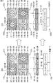
[本技術の手法により構成された単一画素単位]
図3は、本技術の手法により構成された単一画素単位の構成例を示す図である。図3の左側には、一般的な構成の単一画素単位10が示されており、図3の右側には、本技術の手法により構成された単一画素単位100が示されている。
[Single pixel unit configured by this technology]
FIG. 3 is a diagram illustrating a configuration example of a single pixel unit configured by the technique of the present technology. A
図3の左上の図は、隣接する4つの一般的な構成の単一画素単位10乃至13の集合体の上面図である。なお、図3以降に示される上面図においては、オンチップレンズの図示は省略されている。単一画素単位10には、緑用カラーフィルタ22が配置されている。単一画素単位11には、青用カラーフィルタ25が配置されている。単一画素単位12には、赤用カラーフィルタ26が配置されている。単一画素単位13には、緑用カラーフィルタ27が配置されている。
The upper left figure of FIG. 3 is a top view of a group of four adjacent
図3の左下の図は、一般的な構成の単一画素単位10の線L−L’における断面図である。一般的な構成の単一画素単位10は、図1Aを参照して説明したように、1つのフォトダイオード21に対して、1つの緑用カラーフィルタ22および1つのオンチップレンズ23が、下方からその順に積層されて構成される。
3 is a cross-sectional view taken along line L-L ′ of a
このような一般的な構成の単一画素単位10,13に対して、本技術の手法が適用されると、図3の右側に示す構成の単一画素単位100、103(以下、本構成の単一画素単位100、103と称する)が実現される。すなわち、単一画素単位10,13に配置された1つの緑用カラーフィルタ22,27をそれぞれ4分割し、4分割された緑用カラーフィルタ22,27のそれぞれを1対1の割合の数(すなわち2個ずつ)のA用カラーフィルタとB用カラーフィルタに置き換える。これにより、1つの画素単位内の異なる平面位置に、複数のカラーフィルタが配置される。
When the technique of the present technology is applied to the
図3の右上の図は、本構成の単一画素単位100,103、および一般的な構成の単一画素単位101,102の集合体の上面図である。
The upper right diagram in FIG. 3 is a top view of an assembly of
本構成の単一画素単位100には、A用カラーフィルタ112−UL,112−DR、およびB用カラーフィルタ112−UR,112−DLが配置されている。ここで、A用カラーフィルタとは、オンチップレンズから射出された光のうち、A色の波長帯域の光だけを透過するフィルタをいう。一方、B用カラーフィルタとは、オンチップレンズから射出された光のうち、A色の波長帯域とは異なるB色の波長帯域の光だけを透過するフィルタをいう。なお、A用カラーフィルタとB用カラーフィルタは、一般的な緑用カラーフィルタを置き換えたものであることから、一般的な緑用カラーフィルタが透過する波長帯域(略500乃至570nmの範囲)内の任意の範囲(つまり、第1の範囲と、それと異なる第2の範囲)の波長帯域の光を透過するカラーフィルタである。
In the
同様に、本構成の単一画素単位103には、A用カラーフィルタ117−UL,117−DR、およびB用カラーフィルタ117−UR,117−DLが配置されている。すなわち、本構成の単一画素単位100,103には、A用カラーフィルタとB用カラーフィルタが1対1の割合の数(すなわち2個ずつ)で配置されている。
Similarly, in the
一般的な構成の単一画素単位101には、図3の左上の図の一般的な構成の単一画素単位11と同様に、青用カラーフィルタ115が配置されている。また、一般的な構成の単一画素単位102には、図3の左上の図の一般的な構成の単一画素単位12と同様に、赤用カラーフィルタ116が配置されている。
In the
図3の右下の図は、本構成の単一画素単位100の線L−L’における断面図である。
3 is a cross-sectional view taken along line L-L ′ of the
本構成の単一画素単位100は、1つのフォトダイオード111に対して、A用カラーフィルタ112−ULとB用カラーフィルタ112−URの組、オンチップレンズ113−ULとオンチップレンズ113−URの組が下方からその順に積層されて構成される。すなわち、A用カラーフィルタ112−ULの上にオンチップレンズ113−ULが配置され、B用カラーフィルタ112−URの上にオンチップレンズ113−URが配置される。
The
このように、図3の例では、本構成の単一画素単位100には、1つのフォトダイオード111の上に配置されるカラーフィルタとして、A用カラーフィルタ112−UL,112−DRと、B用カラーフィルタ112−UR,112−DLといった、2種類のカラーフィルタが採用され、同一種類のカラーフィルタが対角線上に配置されている。ただし、本構成の単一画素単位に採用されるカラーフィルタは、特に図3の例に限定されず、任意の2種類以上の複数のカラーフィルタであれば足りる。
As described above, in the example of FIG. 3, the
[本技術の手法により構成されたN分割画素単位]
図4は、本技術の手法により構成されたN分割画素単位の構成例を示す図である。図4の左側は、一般的な構成のN分割画素単位30が示されており、図4の右側は、本技術の手法により構成されたN分割画素単位100aが示されている。
[N-divided pixel unit configured by the technique of this technology]
FIG. 4 is a diagram illustrating a configuration example of an N-divided pixel unit configured by the technique of the present technology. The left side of FIG. 4 shows an N-divided
図4の左上の図は、隣接する4つの一般的な構成のN分割画素単位30乃至33の集合体の上面図である。N分割画素単位30には、緑用カラーフィルタ42が配置されている。N分割画素単位31には、青用カラーフィルタ45が配置されている。N分割画素単位32には、赤用カラーフィルタ46が配置されている。N分割画素単位33には、緑用カラーフィルタ47が配置されている。
The upper left figure in FIG. 4 is a top view of an aggregate of four adjacent N-divided
図4の左下の図は、一般的な構成のN分割画素単位30の線L−L’における断面図である。一般的な構成のN分割画素単位30は、図1Bを参照して説明したように、隣接する2つのフォトダイオード41−1,41−2の組に対して、1つの緑用カラーフィルタ42および1つのオンチップレンズ43が、下方からその順に積層されて構成される。
4 is a cross-sectional view taken along line L-L ′ of the N-divided
このような一般的な構成のN分割画素単位30,33に対して、本技術の手法が適用されると、図4の右側に示す本構成のN分割画素単位100a,103aが実現される。すなわちN分割画素単位30,33に配置された1つの緑用カラーフィルタ42,47をそれぞれ4分割し、4分割された緑用カラーフィルタ42,47のそれぞれを1対1の割合の数(すなわち2個ずつ)のA用カラーフィルタとB用カラーフィルタに置き換える。これにより、1つの画素単位内の異なる平面位置に、複数のカラーフィルタが配置される。
When the technique of the present technology is applied to the N-divided
図4の右上の図は、本構成のN分割画素単位100a,103a、および一般的な構成のN分割画素単位101a,102aの集合体の上面図である。
4 is a top view of an assembly of N-divided
本構成のN分割画素単位100aには、A用カラーフィルタ112a−UL,112a−DR、およびB用カラーフィルタ112a−UR,112a−DLが配置されている。同様に、本構成の単一画素単位103aには、A用カラーフィルタ117a−UL,117a−DR、およびB用カラーフィルタ117a−UR,117a−DLが配置されている。すなわち、本構成のN分割画素単位100a,103aには、A用カラーフィルタとB用カラーフィルタが1対1の割合の数(すなわち2個ずつ)で配置されている。
In the N-divided
一般的な構成のN分割画素単位101aには、図4の左上の図の一般的な構成のN分割画素単位31と同様に、青用カラーフィルタ115aが配置されている。また、一般的な構成のN分割画素単位102aには、図4の左上の図の一般的な構成のN分割画素単位32と同様に、赤用カラーフィルタ116aが配置されている。
In the N-divided
図4の右下の図は、本構成のN分割画素単位100aの線L−L’における断面図である。
4 is a cross-sectional view taken along line L-L ′ of the N-divided
本構成のN分割画素単位100aは、隣接する2つのフォトダイオード111a−UL,111a−URの組に対して、A用カラーフィルタ112a−ULとB用カラーフィルタ112a−URの組、オンチップレンズ113a−ULとオンチップレンズ113a−URの組が下方からその順に積層されて構成される。すなわち、フォトダイオード111a−UL、A用カラーフィルタ112a−UL、オンチップレンズ113a−ULが下方からその順に配置され、フォトダイオード111a−UR、B用カラーフィルタ112a−UR、オンチップレンズ113a−URが下方から順に配置される。
The N-divided
このように、図4の例では、本構成のN分割画素単位100aには、N個のフォトダイオードの上に配置されるカラーフィルタとして、A用カラーフィルタ112a−UL,112a−DRと、B用カラーフィルタ112a−UR,112a−DLといった、2種類のカラーフィルタが採用され、同一種類のカラーフィルタが対角線上に配置されている。ただし、本構成のN分割画素単位に採用されるカラーフィルタは、特に図4の例に限定されず、任意の2種類以上の複数個のカラーフィルタであれば足りる。
As described above, in the example of FIG. 4, the N-divided
[出力される光の分光特性]
本構成の画素単位、すなわち1つの画素単位内の異なる平面位置に、複数のカラーフィルタが配置された画素単位においては、フォトダイオードから出力される電気信号は、図5に示されるように、複数のカラーフィルタの分光特性の合成結果となる。
[Spectral characteristics of output light]
In the pixel unit of this configuration, that is, in a pixel unit in which a plurality of color filters are arranged at different plane positions in one pixel unit, as shown in FIG. This is the result of combining the spectral characteristics of the color filter.
図5は、本構成の画素単位における、フォトダイオードから出力される光の分光特性を示す図である。図5において、縦軸は透過率を示し、横軸は波長を示している。 FIG. 5 is a diagram showing the spectral characteristics of the light output from the photodiode in the pixel unit of this configuration. In FIG. 5, the vertical axis indicates the transmittance, and the horizontal axis indicates the wavelength.
本構成の単一画素単位100に配置されるA用カラーフィルタ112−UL,112−DRは、実線で示されるように、波長が520乃至540nm近辺で透過率が最も高くなる特性を有する。また、本構成の単一画素単位100に配置されるB用カラーフィルタ112−UR,112−DLは、点線で示されるように、波長が530乃至580nm近辺で透過率が最も高くなる特性を有する。
The A color filters 112-UL and 112-DR arranged in the
本構成の単一画素単位100に配置されたフォトダイオード111には、このような特性を有するA用カラーフィルタ112−UL,112−DR、B用カラーフィルタ112−UR,112−DLのそれぞれを透過した光が入射する。この場合、フォトダイオード111に入射する光の分光特性は、A用カラーフィルタ112−UL,112−DRとB用カラーフィルタ112−UR,112−DLの特性の合成結果、すなわち、図5において破線で示される出力分光Cの特性となる。したがって、本構成の単一画素単位100においては、出力分光Cに応じたレベルの電気信号がフォトダイオード111から出力される。
In the
同様に、本構成のN分割画素単位100aに配置されたN個のフォトダイオードには、図5に示される特性を有するA用カラーフィルタ112a−UL,112a−DR、B用カラーフィルタ112a−UR,112a−DLのそれぞれを透過した光が入射する。この場合、N個のフォトダイオードに入射する光の分光特性がすべて合成されると、A用カラーフィルタ112a−UL,112a−DRとB用カラーフィルタ112a−UR,112a−DLの特性の合成結果、すなわち、図5において破線で示される出力分光Cの特性となる。したがって、本構成のN分割画素単位100aにおいては、N個のフォトダイオードのそれぞれの受光量に応じたレベルのすべてが加算されたレベルを有する電気信号、すなわち、出力分光Cに応じたレベルの電気信号が、後述する共通FD部201または画像信号読み出し部(例えば後述の図20の画像信号読み出し部533)から出力される。
Similarly, the N photodiodes arranged in the N-divided
このように、本構成の単一画素単位100およびN分割画素単位100aにおいては、1つの画素単位内の異なる平面位置に、図5に示される特性を有するA用カラーフィルタとB用カラーフィルタが1対1の割合で配置されて構成される。これにより、単一画素単位100に配置されたフォトダイオードに集光される光の分光特性は、図5の破線で示される出力分光Cの特性となる。また、N分割画素単位100aのN個のフォトダイオードに入射する光の分光特性がすべて合成されると、図5の破線で示される出力分光Cの特性となる。つまり、本構成の単一画素単位100およびN分割画素単位100aによれば、A用カラーフィルタとB用カラーフィルタの材料による本来の分光特性ではない、新たな分光特性(すなわち、出力分光Cの特性)を創出することができる。すなわち、新たなカラーフィルタの材料開発によらず、新たな分光特性を創出することができる。
As described above, in the
しかしながら、例えば、複数のカラーフィルタが、1つの画素単位内の同一の平面位置に積層されて配置される場合にはフォトダイオードから出力される光の分光特性は、同一の平面位置に積層された複数のカラーフィルタの分光特性の積算結果となる。この詳細について、以下、図6と図7を参照しながら説明する。 However, for example, when a plurality of color filters are arranged in the same plane position in one pixel unit, the spectral characteristics of the light output from the photodiode are laminated in the same plane position. This is a result of integrating spectral characteristics of a plurality of color filters. Details of this will be described below with reference to FIGS. 6 and 7. FIG.
[画素単位内の同一平面位置に配置される複数のカラーフィルタ]
図6は、同一の平面位置に積層されて配置される複数のカラーフィルタを含む単一画素単位の構成例を示す図である。
[Multiple color filters arranged at the same plane position in pixel unit]
FIG. 6 is a diagram illustrating a configuration example of a single pixel unit including a plurality of color filters that are stacked in the same plane position.
図6の左側には、一般的な構成の単一画素単位10が示されている。この一般的な構成の単一画素単位10は、図1A等を参照して説明済みであるので、ここではその説明を省略する。
On the left side of FIG. 6, a
図6の右側には、このような一般的な構成の単一画素単位10に対して、同一の平面位置に積層されて配置される複数のカラーフィルタを含む単一画素単位120が示されている。
The right side of FIG. 6 shows a
詳細には、図6の右上の図は、同一の平面位置に複数のカラーフィルタが積層されて配置された単一画素単位120,123を含む単一画素単位の集合体の上面図である。図6の右下の図は、当該単一画素単位120の線L−L’における断面図である。
Specifically, the upper right diagram in FIG. 6 is a top view of an aggregate of single pixel units including
図6の右上の図および右下の図に示されるように、単一画素単位120は、1つのフォトダイオード131に対して、B用カラーフィルタ132、A用カラーフィルタ133、オンチップレンズ134−Lとオンチップレンズ134−Rの組が下方からその順に積層されて構成される。すなわち、フォトダイオード131が配置されている同一の平面位置において、B用カラーフィルタ132とA用カラーフィルタ133とが積層されて配置されている。
As shown in the upper right diagram and the lower right diagram in FIG. 6, the
[出力される光の分光特性]
図7は、このように同一の平面位置に積層されて配置される複数のカラーフィルタを含む単一画素単位120における、フォトダイオード131から出力される光の分光特性を示す図である。図7において、縦軸は透過率を示し、横軸は波長を示している。
[Spectral characteristics of output light]
FIG. 7 is a diagram showing the spectral characteristics of the light output from the
図7に示されるように、単一画素単位120に配置されるA用カラーフィルタ133は、実線で示されるように、波長が600nm近辺で透過率が最も高くなる特性を有する。また、単一画素単位120に配置されるB用カラーフィルタ132は、点線で示されるように、波長が500nm近辺で透過率が最も高くなる特性を有する。単一画素単位120に配置されたフォトダイオード131には、このような特性を有するA用カラーフィルタ133およびB用カラーフィルタ132の2つのカラーフィルタを透過した光が入射する。
As shown in FIG. 7, the
この場合、フォトダイオード131に入射する光は、B用カラーフィルタ132の特性とA用カラーフィルタ133の特性との積算結果、すなわち、図7において破線で示される出力分光Tの特性となる。これは、単一画素単位120内の同一の平面位置に複数のカラーフィルタが配置された場合、当該複数のカラーフィルタのそれぞれにおいて分光吸収が起きるからである。したがって、単一画素単位120内の同一平面位置にある全てのカラーフィルタの分光特性の積算結果に応じたレベルの電気信号のみがフォトダイオード131から出力される。
In this case, the light incident on the
[本構成の画素単位から出力される光の分光特性]
これに対して、本構成の画素単位において、図7に示されるA用カラーフィルタとB用カラーフィルタを用いた場合、フォトダイオードから出力される光の分光特性は図8のようになる。
[Spectral characteristics of light output from the pixel unit of this configuration]
On the other hand, when the A color filter and the B color filter shown in FIG. 7 are used in the pixel unit of this configuration, the spectral characteristics of the light output from the photodiode are as shown in FIG.
図8は、本構成の画素単位における、フォトダイオードから出力される光の分光特性を示す図である。図8において、縦軸は透過率を示し、横軸は波長を示している。 FIG. 8 is a diagram showing the spectral characteristics of the light output from the photodiode in the pixel unit of this configuration. In FIG. 8, the vertical axis indicates the transmittance, and the horizontal axis indicates the wavelength.
図8に示されるように、本構成の画素単位に配置されるA用カラーフィルタとB用カラーフィルタは、図7を参照して説明した単一画素単位120に配置されるA用カラーフィルタ133とB用カラーフィルタ132と同様の特性を有するとする。
As shown in FIG. 8, the A color filter and the B color filter arranged in the pixel unit of this configuration are the
本構成の単一画素単位100に配置されたフォトダイオード111には、このような特性を有するA用カラーフィルタ112−UL,112−DR、B用カラーフィルタ112−UR,112−DLのそれぞれを透過した光が入射する。この場合、フォトダイオード111に入射する光の分光特性は、A用カラーフィルタ112−UL,112−DRとB用カラーフィルタ112−UR,112−DLの特性の合成結果、すなわち、図8において破線で示される出力分光Cの特性となる。したがって、本構成の単一画素単位100においては、出力分光Cに応じたレベルの電気信号がフォトダイオード111から出力される。
In the
同様に、本構成のN分割画素単位100aに配置されたN個のフォトダイオードには、図8に示される特性を有するA用カラーフィルタ112a−UL,112a−DR、B用カラーフィルタ112a−UR,112a−DLのそれぞれを透過した光が入射する。この場合、N個のフォトダイオードに入射する光の分光特性の合成結果は、A用カラーフィルタ112a−UL,112a−DRとB用カラーフィルタ112a−UR,112a−DLの特性の合成結果、すなわち、図8において破線で示される出力分光Cの特性となる。したがって、本構成のN分割画素単位100aにおいては、N個のフォトダイオードのそれぞれの受光量に応じたレベルのすべてが加算されたレベルを有する電気信号、すなわち、出力分光Cに応じたレベルの電気信号が、後述する共通FD部201または画像信号読み出し部(例えば後述の図20の画像信号読み出し部533)から出力される。
Similarly, the N photodiodes arranged in the N-divided
以上、図3乃至図8を参照して説明したように、本構成の単一画素単位100およびN分割画素単位100aにおいては、1つの画素単位内の異なる平面位置に、複数のカラーフィルタが配置されることにより、新たなカラーフィルタの材料開発によらず、新たな分光特性を創出することができる。
As described above with reference to FIGS. 3 to 8, in the
ここで、1つのカラーフィルタを透過した光を受光する単位が画素であるとするならば、1つの画素単位の異なる平面位置に複数のカラーフィルタが配置される場合には、複数のカラーフィルタの各々に対応して画素が1つずつ存在すること、すなわち1つの画素単位に複数の画素が存在することになる。このように、1つの画素単位に含まれる複数の画素を、一般的な画素と区別すべく、以下、小画素と称する。 Here, assuming that a unit for receiving light transmitted through one color filter is a pixel, when a plurality of color filters are arranged at different plane positions of one pixel unit, One pixel exists corresponding to each, that is, a plurality of pixels exist in one pixel unit. In this way, a plurality of pixels included in one pixel unit are hereinafter referred to as small pixels in order to distinguish them from general pixels.
[オンチップレンズの配置]
さらに、図3と図4を参照して説明したように、本構成の単一画素単位100およびN分割画素単位100aにおいては、オンチップレンズは、1つの画素単位内の異なる平面位置に配置された複数のカラーフィルタ毎、すなわち小画素毎に配置される。
[Placement of on-chip lens]
Further, as described with reference to FIGS. 3 and 4, in the
図9は、オンチップレンズの配置について説明する図である。 FIG. 9 is a diagram illustrating the arrangement of on-chip lenses.
図9の1番左の図は、一般的な構成の単一画素単位10が示されている。この一般的な構成の単一画素単位10は、図1A等を参照して説明済みであるので、ここではその説明を省略する。
The leftmost diagram in FIG. 9 shows a
これに対して、図9の左から2番目の上の図は、1つの画素単位内の異なる平面位置に、複数のカラーフィルタが配置された単一画素単位150,153、および一般的な構成の単一画素単位151,152の集合体の上面図であり、下の図は、単一画素単位150の線L−L’における断面図である。単一画素単位150においては、1つのフォトダイオード161に対して、A用カラーフィルタ162−ULとB用カラーフィルタ162−URの組、1つのオンチップレンズ163が下方からその順に積層されて構成される。
On the other hand, the second upper diagram from the left in FIG. 9 shows
図9の左から2番目の図に示されるように、単一画素単位150には、1つのフォトダイオード161に対して、カラーフィルタは複数配置されるが、オンチップレンズ163は1つのみ配置される。この場合、斜め方向からの光がオンチップレンズ163に入射すると、複数のカラーフィルタを透過する光の量にばらつきが生じて、それに伴いフォトダイオード161に入射する光の分光特性も変動する。すなわち、フォトダイオード161に入射する光の分光特性が、オンチップレンズ163に入射する光の入射角によって変動する。例えば図9の左から2番目の図の例に示されるように、B用カラーフィルタ162−URを透過する光の量よりも、A用カラーフィルタ162−ULを透過する光の量が多くなる場合、フォトダイオード161に入射する光の分光特性が変動する。
As shown in the second diagram from the left in FIG. 9, in the
したがって、図9の左から3番目と4番目の図に示されるように、本構成の単一画素単位100とN分割画素単位100aにおいては、オンチップレンズは、1つの画素単位内の異なる平面位置に配置された複数のカラーフィルタ毎、すなわち小画素毎に配置される。
Accordingly, as shown in the third and fourth diagrams from the left in FIG. 9, in the
本構成の単一画素単位100においては、A用カラーフィルタ112−ULの上にオンチップレンズ113−ULが配置され、B用カラーフィルタ112−URの上にオンチップレンズ113−URが配置される。これにより、A用カラーフィルタ112−ULとB用カラーフィルタ112−URを透過する光の量のばらつきが低減され、フォトダイオード111に入射する光の分光特性の変動が抑制される。
In the
同様に、本構成のN分割画素単位100aにおいても、A用カラーフィルタ112a−ULの上にオンチップレンズ113a−ULが配置され、B用カラーフィルタ112a−URの上にオンチップレンズ113a−URが配置される。これにより、A用カラーフィルタ112a−ULとB用カラーフィルタ112a−URを透過する光の量のばらつきが低減され、フォトダイオード111a−ULとフォトダイオード111a−URに入射する光の分光特性の変動が抑制される。
Similarly, in the N-divided
このように、1つの画素単位内の異なる平面位置に複数のカラーフィルタおよび複数のオンチップレンズが配置されることにより、各画素単位に配置されるフォトダイオードに集光される光が光学的に合成される。これにより、各フォトダイオードに集光される光の分光特性を、用途に合わせた最適なものに制御することができる。 In this way, by arranging a plurality of color filters and a plurality of on-chip lenses at different plane positions in one pixel unit, the light condensed on the photodiodes arranged in each pixel unit is optically reflected. Synthesized. Thereby, the spectral characteristic of the light condensed on each photodiode can be controlled to an optimum one according to the application.
[導波路が設置された本構成の単一画素単位の構成例]
ところで、1つの画素単位内に配置されるフォトダイオードは、インプラの不均一性等により、必ずしも均一な光電変換を行えるとは限らず、フォトダイオードに感度ムラが生じる場合もある。
[Configuration example of single pixel unit of this configuration with waveguides installed]
By the way, a photodiode arranged in one pixel unit does not necessarily perform uniform photoelectric conversion due to non-uniformity of the implantation, and the sensitivity unevenness may occur in the photodiode.
図10は、導波路が設置された本構成の単一画素単位の構成例を示す図である。 FIG. 10 is a diagram showing a configuration example of a single pixel unit of this configuration in which a waveguide is installed.
図10の左側には、一般的な構成の単一画素単位10が示されている。この一般的な構成の単一画素単位10は、図1A等を参照して説明済みであるので、ここではその説明を省略する。
A
図10の中央には、本構成の単一画素単位100が示されている。この本構成の単一画素単位100は、図3の右側の図等を参照して説明済みであるので、ここではその説明を省略する。
In the center of FIG. 10, a
図10の中央下の図に示されるように、例えば、フォトダイオード111に、受光面の端部が低感度であり、中央部が高感度であるような感度ムラが生じているとする。この場合、例えば、A用カラーフィルタ112−ULを透過してフォトダイオード111の端部に入射した光と、B用カラーフィルタ112−URを透過してフォトダイオード111の中央部に入射した光とが同一光量であっても、中央部の方が端部よりも光量が多いものとして高レベルの電気信号が出力される。
As shown in the lower center diagram of FIG. 10, for example, it is assumed that the
したがって、フォトダイオード111に図10の中央下の図に示されるような感度ムラが生じている場合、例えば、図10の右下の図に示されるように、フォトダイオード111の上方に導波路169を配置する。これにより、A用カラーフィルタ112−ULを透過した光とB用カラーフィルタ112−URを透過した光は、導波路169により一旦集光されて、感度の高いフォトダイオード111の中央部に入射される。したがって、A用カラーフィルタ112−ULを透過した光と、B用カラーフィルタ112−URを透過した光とが同一光量であった場合には、同一レベルの電気信号が出力される。
Accordingly, when the sensitivity unevenness as shown in the lower center diagram of FIG. 10 occurs in the
このように、本構成の単一画素単位100に導波路169が配置されることにより、フォトダイオード111の感度ムラによる影響を低減させながら、フォトダイオード111に集光される光が光学的に合成される。これにより、各フォトダイオードに集光される光の分光特性を、用途に合わせた最適なものに制御することができる。
As described above, by arranging the
以上のように、本構成の画素単位によれば、フォトダイオードに集光される光の分光特性を、光学的な合成により制御することができる。以下では、フォトダイオードに集光される光の分光特性を、電気的な合成により制御する例について説明する。 As described above, according to the pixel unit of this configuration, the spectral characteristics of the light condensed on the photodiode can be controlled by optical synthesis. Below, the example which controls the spectral characteristics of the light condensed on a photodiode by electrical synthesis will be described.
[第1の加算の手法が適用されたN分割画素単位]
N分割画素単位においては、N個のフォトダイオードのそれぞれの受光量に応じたレベルのすべてが加算されたレベルを有する電気信号が出力される。上述したように、N個のフォトダイオードのそれぞれの電気信号の加算の手法として第1の手法と第2の手法がある。
[N-divided pixel unit to which the first addition method is applied]
In the N-divided pixel unit, an electric signal having a level obtained by adding all levels according to the amounts of light received by the N photodiodes is output. As described above, there are the first method and the second method as methods for adding electric signals of N photodiodes.
図11は、第1の加算の手法が適用されたN分割画素単位の構成例を示す図である。 FIG. 11 is a diagram illustrating a configuration example of an N-divided pixel unit to which the first addition method is applied.
図11の左側には、第1の加算の手法が適用された一般的な構成のN分割画素単位170が示されており、図11の右側には、第1の加算の手法が適用された本構成のN分割画素単位100bが示されている。
The left side of FIG. 11 shows an N-divided
図11の左上の図は、第1の加算の手法が適用された隣接する4つの一般的な構成のN分割画素単位170乃至173の集合体の上面図である。
The upper left diagram in FIG. 11 is a top view of an aggregate of four adjacent general N-divided
N分割画素単位170には、4つの緑用カラーフィルタ182−UL,182−UR,182−DL,182−DRが配置されている。また、4つの緑用カラーフィルタのそれぞれには、三角で示される転送ゲート200が配置されている。さらに、4つの緑用カラーフィルタの中心部の位置には、共通FD部201が配置されている。
In the N-divided
N分割画素単位171には、4つの青用カラーフィルタ185−UL,185−UR,185−DL,185−DRが配置されている。また、4つの青用カラーフィルタのそれぞれには、転送ゲート200が配置されている。さらに、4つの青用カラーフィルタの中心部の位置には、共通FD部201が配置されている。
In the N-divided
N分割画素単位172には、4つの赤用カラーフィルタ186−UL,186−UR,186−DL,186−DRが配置されている。また、4つの赤用カラーフィルタのそれぞれには、転送ゲート200が配置されている。さらに、4つの赤用カラーフィルタの中心部の位置には、共通FD部201が配置されている。
In the N-divided pixel unit 172, four red color filters 186-UL, 186-UR, 186-DL, and 186-DR are arranged. A
N分割画素単位173には、4つの緑用カラーフィルタ187−UL,187−UR,187−DL,187−DRが配置されている。また、4つの緑用カラーフィルタのそれぞれには、転送ゲート200が配置されている。さらに、4つの緑用カラーフィルタの中心部の位置には、共通FD部201が配置されている。
In the N-divided
そして、図11の左下の図に示されるように、第1の加算の手法によれば、N分割画素単位170の4つの緑用フォトダイオード181−UL,181−UR,181−DL,181−DRの各受光量に応じた各レベルの電気信号が、転送ゲート200にそれぞれ転送されて、その後共通FD部201にそれぞれ転送される。共通FD部201においてすべての電気信号の加算信号、すなわち各レベルが総加算されたレベルを有する電気信号が出力される。なお、共通FD部201は、蓄積されたすべての電荷を同時に読み出すことで、読み出された電荷分のレベルの電気信号を加算する。このように、第1の加算の手法においては、N個(この場合4個)のフォトダイオードのそれぞれからの電気信号のレベルがすべて加算され、総加算後のレベルの電気信号が、N分割画素単位170から出力される。
Then, as shown in the lower left diagram of FIG. 11, according to the first addition method, four green photodiodes 181 -UL, 181 -UR, 181 -DL, 181-of the N-divided
N分割画素単位171乃至173においても同様に、各フォトダイオードの各受光量に応じた各レベルの電気信号が、転送ゲート200にそれぞれ転送されて、その後共通FD部201にそれぞれ転送される。そして、共通FD部201においてすべての電気信号の総加算後のレベルの電気信号が、N分割画素単位171乃至173のそれぞれから出力される。
Similarly, in the N-divided
これに対して、図11の右上の図は、第1の加算の手法が適用された本構成のN分割画素単位100b,103b、および一般的な構成のN分割画素単位101b,102bの集合体の上面図である。
On the other hand, the upper right diagram in FIG. 11 shows an assembly of N-divided
本構成のN分割画素単位100bには、A用カラーフィルタ112b−UL,112b−DR、およびB用カラーフィルタ112b−UR,112b−DLが配置されている。また、4つのカラーフィルタのそれぞれには、三角で示される転送ゲート210が配置されている。さらに、4つのカラーフィルタの中心部の位置には、共通FD部211が配置されている。
In the N-divided
一般的な構成のN分割画素単位101bには、4つの青用カラーフィルタ115b−UL,115b−UR,115b−DL,115b−DRが配置されている。また、4つの青用カラーフィルタのそれぞれには、転送ゲート210が配置されている。さらに、4つの青用カラーフィルタの中心部の位置には、共通FD部211が配置されている。
Four
一般的な構成のN分割画素単位102bには、4つの赤用カラーフィルタ116b−UL,116b−UR,116b−DL,116b−DRが配置されている。また、4つの赤用カラーフィルタのそれぞれには、転送ゲート210が配置されている。さらに、4つの赤用カラーフィルタの中心部の位置には、共通FD部211が配置されている。
Four
本構成のN分割画素単位103bには、B用カラーフィルタ117b−UL,117b−DR、およびA用カラーフィルタ117b−UR,117b−DLが配置されている。また、4つのカラーフィルタのそれぞれには、転送ゲート210が配置されている。さらに、4つのカラーフィルタの中心部の位置には、共通FD部211が配置されている。
そして、図11の右下の図に示されるように、第1の加算の手法によれば、本構成のN分割画素単位100bのA用フォトダイオード111b−UL,111b−DR、およびB用フォトダイオード111b−UR,111b−DLの各受光量に応じた各レベルの電気信号が、転送ゲート210にそれぞれ転送されて、その後共通FD部211に転送される。共通FD部211においてすべての電気信号の加算信号、すなわち各レベルが総加算されたレベルを有する電気信号が、N分割画素単位100bから出力される。なお、共通FD部211は、蓄積されたすべての電荷を同時に読み出すことで、読み出された電荷分のレベルの電気信号を加算する。
Then, as shown in the lower right diagram of FIG. 11, according to the first addition method, the
N分割画素単位101b乃至103bにおいても同様に、各フォトダイオードの各受光量に応じた各レベルの電気信号が、転送ゲート210にそれぞれ転送されて、その後共通FD部211にそれぞれ転送される。
Similarly, in the N-divided
この場合、本構成のN分割画素単位100bおよび103bから出力される光の分光特性は、図5において点線で示される出力分光Cの特性となる。すなわち、N分割画素単位100bおよび103b内の異なる平面位置に配置された複数のカラーフィルタの分光特性の合成結果に応じたレベルの電気信号が、N分割画素単位100bおよび103bから出力される。つまり、本構成のN分割画素単位100bおよび103bによれば、A用カラーフィルタとB用カラーフィルタの材料による本来の分光特性ではない、新たな分光特性を創出することができる。
In this case, the spectral characteristic of the light output from the N-divided
[ゲインによる分光特性の調整]
図11の右側の本構成のN分割画素単位100bおよび103bにおいては、共通FD部211は、複数のフォトダイオードの各受光量に応じた各レベルの電気信号を同時に読み出してそのまま加算した。しかしながら、共通FD部211は、同じ分光特性の光を受光するフォトダイオード毎に異なるタイミングで読み出してから、それぞれ個別に設定されたゲインでレベルが増幅された電気信号を加算してもよい。
[Adjust spectral characteristics by gain]
In the N-divided
ここで、図11の右側の本構成のN分割画素単位100bおよび103bにおいて、1対1の割合の数で配置されたA用カラーフィルタとB用カラーフィルタを、例えば、図12に示される特性を有するD用カラーフィルタとE用カラーフィルタにそれぞれ置き換えたとする。
Here, in the N-divided
図12は、1対1の割合の数でD用カラーフィルタとE用カラーフィルタが配置された本構成のN分割画素単位100bおよび103bにおける、フォトダイオードから出力される光の分光特性を示す図である。図12において、縦軸は透過率を示し、横軸は波長を示している。
FIG. 12 is a diagram showing the spectral characteristics of the light output from the photodiodes in the N-divided
図12に示されるように、本構成のN分割画素単位100bおよび103bに配置されるD用カラーフィルタは、実線で示されるように、波長が520乃至540近辺で透過率が最も高くなる特性を有する。また、本構成のN分割画素単位100bおよび103bに配置されるE用カラーフィルタは、点線で示されるように、波長が540乃至590近辺で透過率が最も高くなる特性を有する。
As shown in FIG. 12, the color filter for D arranged in the N-divided
この場合、本構成のN分割画素単位100bおよび103bに配置される共通FD部211は、D用カラーフィルタとE用カラーフィルタの分光特性に応じたレベルの電気信号を、異なるタイミングで読み出してからそのまま加算してもよい。これにより、カラーフィルタの種類と同じ数の電気信号、すなわちこの場合、2種類の電気信号を得ることが可能となる。
In this case, the
さらに、共通FD部211は、同じ分光特性の光を受光するフォトダイオード毎に異なるタイミングで読み出してから、それぞれ個別に設定されたゲインでレベルが増幅された各電気信号を加算してもよい。なお、ゲインは、後段の画像信号読み出し部(例えば後述の図20の画像信号読み出し部533)により設定される。
Further, the
例えば、E用カラーフィルタを透過してフォトダイオードに入射した光の受光量に応じたレベルの電気信号のゲインが5倍に設定されると、図12の一点鎖線で示されるように、波長が540乃至590近辺で、透過率がE用カラーフィルタの透過率の5倍に増幅された特性となる。 For example, when the gain of the electric signal at a level corresponding to the amount of light received through the color filter for E and incident on the photodiode is set to 5 times, the wavelength is changed as shown by the one-dot chain line in FIG. In the vicinity of 540 to 590, the transmittance is amplified to five times the transmittance of the E color filter.
したがって、本構成のN分割画素単位100bおよび103bにおいては、カラーフィルタDの分光特性とカラーフィルタEのゲインが5倍された分光特性の合成結果、すなわち図12において点線で示される出力分光Fの特性に応じたレベルの電気信号が出力される。このように、同じ分光特性の光を受光するフォトダイオード毎に異なるタイミングで読み出されてから、それぞれ個別に設定されたゲインでレベルが増幅された各電気信号が加算されることにより、新たな分光特性を創出することができる。このように、複数のカラーフィルタの分光特性を電気的に合成することにより、用途に応じて最適に、分光特性を制御することができる。
Therefore, in the N-divided
[第2の加算の手法が適用されたN分割画素単位]
次に、第2の加算の手法が適用されたN分割画素単位について説明する。
[N-divided pixel unit to which the second addition method is applied]
Next, an N-divided pixel unit to which the second addition method is applied will be described.
図13は、第2の加算の手法が適用されたN分割画素単位の構成例を示す図である。 FIG. 13 is a diagram illustrating a configuration example of an N-divided pixel unit to which the second addition method is applied.
図13の上の図は、第2の加算の手法が適用された本構成のN分割画素単位100c,103c、および一般的な構成のN分割画素単位101c,102cの集合体の上面図である。
The upper part of FIG. 13 is a top view of an assembly of the N-divided
本構成のN分割画素単位100cには、A用カラーフィルタ112c−UL,112c−DR、およびB用フォトダイオード112c−UR,112c−DLが配置されている。また、4つのカラーフィルタのそれぞれには、三角で示される転送ゲートおよび個別FD部220が配置されている。すなわち、転送ゲートおよび個別FD部220は、転送ゲートと個別FD部が同一の位置に積層されている。
In the N-divided
一般的な構成のN分割画素単位101cには、4つの青用カラーフィルタ115c−UL,115c−UR,115c−DL,115c−DRが配置されている。また、4つの青用カラーフィルタのそれぞれには、転送ゲートおよび個別FD部220が配置されている。
Four
一般的な構成のN分割画素単位102cには、4つの赤用カラーフィルタ116c−UL,116c−UR,116c−DL,116c−DRが配置されている。また、4つの赤用カラーフィルタのそれぞれには、転送ゲートおよび個別FD部220が配置されている。
Four
本構成のN分割画素単位103cには、B用カラーフィルタ117c−UL,117c−DR、およびA用カラーフィルタ117c−UR,117c−DLが配置されている。また、4つのカラーフィルタのそれぞれには、転送ゲートおよび個別FD部220が配置されている。
そして、図13の下の図に示されるように、第2の加算の手法によれば、本構成のN分割画素単位100cのA用フォトダイオード111c−UL,111c−DR、およびB用フォトダイオード111c−UR,111c−DLの各受光量に応じた各レベルの電気信号が、転送ゲートおよび個別FD部220にそれぞれ転送される。そして、転送ゲートおよび個別FD部220のそれぞれから個々に出力された電気信号の全てが、後段の画像信号読み出し部(例えば後述の図20の画像信号読み出し部533)において加算される。
Then, as shown in the lower diagram of FIG. 13, according to the second addition method, the
N分割画素単位101c乃至103cにおいても同様に、各フォトダイオードの各受光量に応じた各レベルの電気信号が、転送ゲートおよび個別FD部220にそれぞれ転送されて、その後後段の画像信号読み出し部(例えば後述の図20の画像信号読み出し部533)において加算される。
Similarly, in the N-divided
この場合、本構成のN分割画素単位100cおよび103cから出力される光の分光特性は、図5において点線で示される特性となる。すなわち、N分割画素単位100cおよび103c内の異なる平面位置に配置された複数のカラーフィルタの分光特性の合成結果に応じたレベルの電気信号が、N分割画素単位100cおよび103cから出力される。つまり、本構成のN分割画素単位100cおよび103cによれば、A用カラーフィルタとB用カラーフィルタの材料による本来の分光特性ではない、新たな分光特性を創出することができる。
In this case, the spectral characteristic of the light output from the N-divided
第2の加算の手法が適用された本構成のN分割画素単位100cおよび103cにおいても、第1の加算の手法が適用された本構成のN分割画素単位100bおよび103bと同様に、例えば、図12に示される特性を有するD用カラーフィルタとE用カラーフィルタにそれぞれ置き換えたとする。
In the N-divided
この場合、第2の加算の手法が適用された本構成のN分割画素単位100cおよび103cにおいても、D用カラーフィルタとE用カラーフィルタの分光特性に応じたレベルの電気信号を、異なるタイミングまたは同一のタイミングで読み出してから、図示せぬ画像信号読み出し部で加算してもよい。これにより、カラーフィルタの種類と同じ数の電気信号、すなわちこの場合、2種類の電気信号を得ることが可能となる。
In this case, also in the N-divided
さらに、後段の画像信号読み出し部(例えば後述の図20の画像信号読み出し部533)は、各レベルの電気信号を加算する前に、同じ分光特性を有する光毎に異なるゲインを設定し、異なるタイミングまたは同一のタイミングで読み出してから、各ゲインでそれぞれ増幅されたレベルの電気信号を加算してもよい。これにより、第2の加算の手法が適用された本構成のN分割画素単位100cおよび103cにおいても、新たな分光特性を創出することができる。このように、複数のカラーフィルタの分光特性を電気的に合成することにより、用途に応じて最適に、分光特性を制御することができる。
Further, the subsequent image signal readout unit (for example, the image
なお、図11の右側と図13を用いて説明した本構成のN分割画素単位においては、N個のフォトダイオードのそれぞれの電気信号が、すべて加算されてから出力されるか、出力されてからすべて加算された。しかしながら、本構成のN分割画素単位においては、N個のフォトダイオードのそれぞれの電気信号を加算せずに独立して出力し、1つの電気信号としてそのまま後段の画像処理部(例えば後述の図20の画像処理部515)で信号処理に用いることもできる。 Note that, in the N-divided pixel unit of the present configuration described with reference to the right side of FIG. 11 and FIG. 13, all the electrical signals of the N photodiodes are output after being added or output. All were added. However, in the N-divided pixel unit of this configuration, the electrical signals of the N photodiodes are output independently without being added, and are directly output as a single electrical signal (for example, FIG. 20 described later). The image processing unit 515) can also be used for signal processing.
例えば、リニアマトリックスにおける演算では、演算に使用できる色に対応する電気信号の種類が多いほど、出力される画像の色再現性は高くなる。したがって、例えば、緑用フォトダイオードの一部をエメラルド用フォトダイオードに置き換えることにより、演算に使用できる色に対応する電気信号の種類を増やして、色再現性を向上させる技術が存在する。しかしながら、緑用フォトダイオードの一部をエメラルド用フォトダイオードに置き換えることにより、緑用フォトダイオードの数の減少に伴う解像度の劣化が生じる場合がある。 For example, in the calculation in the linear matrix, the color reproducibility of the output image becomes higher as the number of types of electric signals corresponding to the colors that can be used in the calculation increases. Therefore, for example, there is a technique for improving the color reproducibility by replacing some of the green photodiodes with emerald photodiodes to increase the types of electrical signals corresponding to colors that can be used for computation. However, when a part of the green photodiode is replaced with the emerald photodiode, resolution may be deteriorated due to a decrease in the number of green photodiodes.
これに対して、本構成のN分割画素単位において、エメラルド用フォトダイオードが用いられた場合、1つの画素単位内に緑用フォトダイオードとエメラルド用フォトダイオードが配置されるため、結果的に緑用フォトダイオードの数も減少せず、解像度の劣化が生じない。 On the other hand, when an emerald photodiode is used in the N-divided pixel unit of the present configuration, the green photodiode and the emerald photodiode are arranged in one pixel unit. The number of photodiodes does not decrease, and resolution does not deteriorate.
このように、本構成のN分割画素単位においては、N個のフォトダイオードのそれぞれの電気信号を、個別に信号処理に用いることができるので、信号処理に使用できる色に対応する電気信号の数を増やすことができる。したがって、解像度劣化を起こさずに色再現性を向上させることができる。 In this way, in the N-divided pixel unit of this configuration, each electrical signal of the N photodiodes can be individually used for signal processing, so the number of electrical signals corresponding to colors that can be used for signal processing. Can be increased. Therefore, color reproducibility can be improved without causing resolution degradation.
本構成のN分割画素単位においては、上述したように、N個のフォトダイオードのそれぞれからの電気信号のレベルの出力手法として、次の3つの手法がある。第1の手法とは、N個のフォトダイオードのそれぞれからの電気信号のレベルを単純に総加算して、総加算後のレベルの電気信号を出力する手法である。第2の手法とは、N個のフォトダイオードのそれぞれからの電気信号のレベルを、個別に設定した異なるゲインでそれぞれ増幅した後に総加算して、総加算後のレベルの電気信号を出力する手法である。第3の手法とは、N個のフォトダイオードのそれぞれからの電気信号をそれぞれ独立して出力する手法である。このような3つの出力手法を選択的に適用することで、異なる複数の出力を得ることができる。 In the N-divided pixel unit of this configuration, as described above, there are the following three methods for outputting the level of the electric signal from each of the N photodiodes. The first method is a method in which the levels of electric signals from each of the N photodiodes are simply added together and an electric signal having a level after the total addition is output. The second method is a method of amplifying the levels of the electric signals from each of the N photodiodes with different gains that are individually set and then adding the total, and outputting the electric signal of the level after the total addition. It is. The third method is a method of independently outputting electric signals from each of the N photodiodes. By selectively applying these three output methods, a plurality of different outputs can be obtained.
このような複数の出力は、転送ゲートや個別FDによる転送のタイミングの制御、電気信号の加算のON/OFFの制御、または後段の制御部(例えば後述の図20の制御部514)の制御により切り替えることが可能である。したがって、同一の撮像素子であっても、このような制御が行われることにより、用途(例えば、一般カメラ、医療機器等)や状況(例えば、色温度、照度等)によって、複数の異なる分光特性を有する出力を得ることができる撮像素子に変化させることができる。 Such a plurality of outputs can be controlled by control of transfer timing by transfer gates or individual FDs, ON / OFF control of addition of electric signals, or control of a control unit at a later stage (for example, control unit 514 in FIG. 20 described later). It is possible to switch. Therefore, even with the same image sensor, by performing such control, a plurality of different spectral characteristics depending on the application (eg, general camera, medical device, etc.) and the situation (eg, color temperature, illuminance, etc.) It is possible to change to an image sensor that can obtain an output having
[ワイドダイナミックレンジ化の適用]
本構成のN分割画素単位においては、図14に示されるように、小画素毎に光(電荷)の蓄積時間を変えることで、ワイドダイナミックレンジ化が可能となる。
[Application of wide dynamic range]
In the N-divided pixel unit of this configuration, as shown in FIG. 14, a wide dynamic range can be achieved by changing the accumulation time of light (charge) for each small pixel.
図14は、小画素毎に電荷の蓄積時間が変えられた本構成のN分割画素単位について説明する図である。 FIG. 14 is a diagram illustrating an N-divided pixel unit of this configuration in which the charge accumulation time is changed for each small pixel.
図14は、第1の加算の手法が適用された本構成のN分割画素単位100b,103b、および一般的な構成のN分割画素単位101b,102bの集合体の上面図である。これについては、図11等を参照して説明済みであるので、ここではその説明を省略する。
FIG. 14 is a top view of an assembly of N-divided
図14の左側のN分割画素単位100b乃至103bにおいては、小画素における電荷の蓄積時間は同一である。
In the N divided
これに対して、図14の右側に示されるN分割画素単位100b乃至103bにおいては、図14に示されるように、小画素毎に電荷の蓄積時間が変えられている。
On the other hand, in the N-divided
具体的には、本構成のN分割画素単位100bに配置されるA用カラーフィルタ112b−ULおよびB用カラーフィルタ112b−URは、長時間の蓄積時間(以下、長蓄積と称する)とする。これに対して、本構成のN分割画素単位100bに配置されるA用カラーフィルタ112b−DLおよびB用カラーフィルタ112b−DRは、短時間の蓄積時間(以下、短蓄積と称する)とする。
Specifically, the
一般的な構成のN分割画素単位101bにおいても、青用カラーフィルタ115b−UL,115b−URは、長蓄積とし、青用カラーフィルタ115b−DL,115b−DRは、短蓄積とする。
Also in the N-divided
一般的な構成のN分割画素単位102bにおいても、青用カラーフィルタ116b−UL,116b−URは、長蓄積とし、青用カラーフィルタ116b−DL,116b−DRは、短蓄積とする。
Also in the N-divided
本構成のN分割画素単位103bに配置されるB用カラーフィルタ117b−ULおよびA用カラーフィルタ117b−URは、長蓄積し、A用カラーフィルタ117b−DLおよびB用カラーフィルタ117b−DRは、短蓄積とする。
The
この場合、N分割画素単位100b乃至103bにおいては、長蓄積の小画素および短蓄積の小画素のそれぞれに、A用カラーフィルタおよびB用カラーフィルタの両方が配置されている。したがって、N分割画素単位100b乃至103bにおいては、長蓄積の小画素および短蓄積の小画素の両方において、A用カラーフィルタおよびB用カラーフィルタの分光特性の合成結果である新たな分光特性を有する出力が得られる。すなわち、本構成のN分割画素単位によれば、ワイドダイナミックレンジ化を適用しながら、新たな分光特性を有する出力を得ることができる。
In this case, in the N-divided
[画素単位に配置されるカラーフィルタの例]
上述の例では、本構成の画素単位においては、緑用カラーフィルタが複数のカラーフィルタ(すなわち、A用カラーフィルタとB用カラーフィルタ)に置き換えられた。しかしながら、その他の色のカラーフィルタ、例えば赤用カラーフィルタ、青用カラーフィルタが複数のカラーフィルタに置き換えられてもよい。また、本構成の画素単位においては、顔料系または染料系のどちらの素材のカラーフィルタが配置されてもよい。また、本構成の画素単位は、ベイヤ配列、クリアビット配列、またはその他の配列で配置される画素に対して適用することができる。
[Example of color filter arranged in pixel unit]
In the example described above, in the pixel unit of this configuration, the green color filter is replaced with a plurality of color filters (that is, the A color filter and the B color filter). However, other color filters such as a red color filter and a blue color filter may be replaced with a plurality of color filters. In addition, in the pixel unit of this configuration, a color filter of either a pigment-based material or a dye-based material may be disposed. The pixel unit of this configuration can be applied to pixels arranged in a Bayer array, a clear bit array, or other arrays.
また、上述の例では、本構成の画素単位においては、緑用カラーフィルタが4分割されて、それぞれが1対1の割合の数の複数のカラーフィルタ(すなわち、A用カラーフィルタ2個とB用カラーフィルタ2個)に置き換えられた。しかしながら、分割数(すなわち小画素の数)も、複数のカラーフィルタの数の割合もこれに限定されない。 In the above-described example, in the pixel unit of this configuration, the green color filter is divided into four, each having a number of color filters in a ratio of 1: 1 (that is, two A color filters and B 2 color filters). However, the number of divisions (that is, the number of small pixels) and the ratio of the number of color filters are not limited to this.
上述の例では、本構成の画素単位においては、A用カラーフィルタとB用カラーフィルタが1対1の割合(すなわち、2個ずつ)で配置された。したがって、本構成の画素単位から出力される光は、図5の出力分光Cに示されるように、A用カラーフィルタとB用カラーフィルタの特性の合成結果として、A用カラーフィルタとB用カラーフィルタの特性の中間の特性を示す分光特性を有する。これに対して、例えば、A用カラーフィルタとB用カラーフィルタが3対1の割合で配置された場合、本構成の画素単位から出力される光は、A用カラーフィルタとB用カラーフィルタの特性の合成結果として、図5のA用カラーフィルタの分光特性により近い特性を有するものとなる。 In the above-described example, in the pixel unit of this configuration, the A color filter and the B color filter are arranged at a ratio of 1 to 1 (that is, 2 each). Therefore, as shown in the output spectrum C of FIG. 5, the light output from the pixel unit of this configuration is obtained by combining the characteristics of the A color filter and the B color filter. It has a spectral characteristic indicating a characteristic intermediate between the characteristics of the filter. On the other hand, for example, when the color filter for A and the color filter for B are arranged at a ratio of 3 to 1, the light output from the pixel unit of this configuration is transmitted from the color filter for A and the color filter for B. As a result of the synthesis of the characteristics, the characteristics closer to the spectral characteristics of the color filter for A in FIG. 5 are obtained.
本構成の画素単位においては、1つの画素単位に配置できるカラーフィルタの数は、最大で、画素単位の分割数、すなわち小画素の数とすることができる。図15を用いて、3つのカラーフィルタが配置された本構成のN分割画素単位について説明する。 In the pixel unit of this configuration, the maximum number of color filters that can be arranged in one pixel unit can be the number of divisions in pixel units, that is, the number of small pixels. The N-divided pixel unit of this configuration in which three color filters are arranged will be described with reference to FIG.
図15は、3つのカラーフィルタが配置された本構成のN分割画素単位100d,103d、および一般的な構成のN分割画素単位101d,102dの集合体の上面図である。
FIG. 15 is a top view of an assembly of N-divided
本構成のN分割画素単位100dには、A用カラーフィルタ112d−UL、B用カラーフィルタ112d−UR,112d−DL、およびC用カラーフィルタ112dのDRが配置されている。すなわち、本構成のN分割画素単位100dには、A用カラーフィルタ、B用カラーフィルタ、およびC用カラーフィルタが、1対2対1の数の割合で配置されている。
In the N-divided
同様に、本構成のN分割画素単位103dには、A用カラーフィルタ117d−UL、B用カラーフィルタ117d−UR,117d−DL、およびC用カラーフィルタ117d−DRが配置されている。すなわち、本構成のN分割画素単位103dには、A用カラーフィルタ、B用カラーフィルタ、およびC用カラーフィルタが、1対2対1の数の割合で配置されている。なお、C用カラーフィルタとは、A色の波長帯域およびB色の波長帯域とは異なるC色の波長帯域の光だけを透過するフィルタをいう。
Similarly, an
一般的な構成のN分割画素単位101dには、青用カラーフィルタ115dが配置されている。また、一般的な構成のN分割画素単位102dには、赤用カラーフィルタ116dが配置されている。
A
このような本構成のN分割画素単位100d,103dにおける、フォトダイオードから出力される光の分光特性は、図16に示されるように、A用カラーフィルタ、B用カラーフィルタ、およびC用カラーフィルタの分光特性の合成結果となる。
The spectral characteristics of the light output from the photodiode in the N-divided
図16は、本構成のN分割画素単位100d,103dにおける、フォトダイオードから出力される光の分光特性を示す図である。図16において、縦軸は透過率を示し、横軸は波長を示している。
FIG. 16 is a diagram showing the spectral characteristics of the light output from the photodiodes in the N-divided
図16に示されるように、本構成のN分割画素単位100d,103dに配置されるA用カラーフィルタは、実線で示されるように、波長が550nm近辺で透過率が最も高くなる特性を有する。また、本構成のN分割画素単位100d,103dに配置されるB用カラーフィルタは、点線で示されるように、波長が510nm近辺で透過率が最も高くなる特性を有する。また、本構成のN分割画素単位100d,103dに配置されるC用カラーフィルタは、一点鎖線で示されるように、波長が530nm近辺で透過率が最も高くなる特性を有する。
As shown in FIG. 16, the color filter for A arranged in the N-divided
この場合、本構成のN分割画素単位100d,103dに配置されるフォトダイオードに入射する光の分光特性は、A用カラーフィルタ、B用カラーフィルタ、およびC用カラーフィルタの特性の合成結果、すなわち、図16において破線で示される出力分光Gの特性となる。したがって、本構成のN分割画素単位100d,103dにおいては、出力分光Gに応じたレベルの電気信号がフォトダイオードから出力される。
In this case, the spectral characteristics of the light incident on the photodiodes arranged in the N-divided
なお、図15に示されるカラーフィルタの配置は、本構成の単一画素単位においても同様に適用することができる。この場合の本構成の単一画素単位における、フォトダイオードから出力される光の分光特性は、図16と同様に、出力分光Gの特性となる。したがって、本構成の単一画素単位においても、出力分光Gに応じたレベルの電気信号がフォトダイオードから出力される。 Note that the arrangement of the color filters shown in FIG. 15 can be similarly applied to a single pixel unit of this configuration. In this case, the spectral characteristic of the light output from the photodiode in the single pixel unit of the present configuration is the characteristic of the output spectral G as in FIG. Therefore, even in a single pixel unit of this configuration, an electric signal having a level corresponding to the output spectrum G is output from the photodiode.
このように、本構成の画素単位によれば、配置される複数のカラーフィルタの数と種類を変えることによって、新たな分光特性を創出することができる。 As described above, according to the pixel unit of this configuration, new spectral characteristics can be created by changing the number and types of the plurality of arranged color filters.
さらに、本構成の画素単位に配置される複数のカラーフィルタの組み合わせは、緑用カラーフィルタ、赤用カラーフィルタ、青用カラーフィルタに限定されず、任意の波長帯域の光を透過するカラーフィルタが組み合わされてもよい。例えば、すべての波長帯域の光を透過する透明なホワイト用カラーフィルタが組み合わされてもよい。ホワイト用カラーフィルタについては、例えば、特開2009−296276号公報等に記載されている。 Further, the combination of the plurality of color filters arranged in the pixel unit of this configuration is not limited to the green color filter, the red color filter, and the blue color filter, and a color filter that transmits light of an arbitrary wavelength band is used. They may be combined. For example, a transparent white color filter that transmits light in all wavelength bands may be combined. The white color filter is described in, for example, Japanese Patent Application Laid-Open No. 2009-296276.
また、本構成の画素単位には、例えば、赤外光や紫外光を透過するカラーフィルタが配置されてもよい。赤外光を透過するカラーフィルタが配置された本構成のN分割画素単位について図17を参照して説明する。 In addition, for example, a color filter that transmits infrared light or ultraviolet light may be disposed in the pixel unit of this configuration. An N-divided pixel unit of this configuration in which a color filter that transmits infrared light is arranged will be described with reference to FIG.
[赤外光カラーフィルタが配置された本構成のN分割画素単位]
図17は、赤外光カラーフィルタが配置された本構成のN分割画素単位構成例を示す図である。
[N-divided pixel unit of this configuration with infrared color filter]
FIG. 17 is a diagram illustrating an example of the N-divided pixel unit configuration of the present configuration in which an infrared light color filter is disposed.
図17の上の図は、本構成のN分割画素単位250,252,253、および一般的な構成のN分割画素単位251の集合体の上面図である。
The upper diagram of FIG. 17 is a top view of an assembly of N-divided
本構成のN分割画素単位250は、赤用カラーフィルタをI用カラーフィルタとJ用カラーフィルタに置き換えたものである。すなわち、本構成のN分割画素単位250には、I用カラーフィルタ262−UL,262−DR、およびJ用カラーフィルタ262−UR,262−DLが配置されている。また、4つのカラーフィルタのそれぞれには、転送ゲート210が配置されている。さらに、4つのカラーフィルタの中心部の位置には、共通FD部211が配置されている。
The N-divided
ここで、I用カラーフィルタとJ用カラーフィルタの分光特性について、図18を参照して説明する。 Here, spectral characteristics of the I color filter and the J color filter will be described with reference to FIG.
図18は、I用カラーフィルタとJ用カラーフィルタの分光特性を示す図である。図18において、縦軸は透過率を示し、横軸は波長を示している。 FIG. 18 is a diagram illustrating spectral characteristics of the I color filter and the J color filter. In FIG. 18, the vertical axis represents the transmittance, and the horizontal axis represents the wavelength.
I用カラーフィルタは、実線で示されるように、波長が600nm近辺で透過率が最も高くなる特性を有する。また、J用カラーフィルタは、点線で示されるように、波長が800nm近辺で透過率が最も高くなる特性を有する。このように、I用カラーフィルタとJ用カラーフィルタは、一般的な赤外光カラーフィルタが透過する波長帯域(略700乃至1000nm)内の光を透過するカラーフィルタである。 As indicated by the solid line, the color filter for I has a characteristic that the transmittance is highest when the wavelength is around 600 nm. In addition, the J color filter has a characteristic that the transmittance is highest when the wavelength is around 800 nm, as indicated by a dotted line. As described above, the color filter for I and the color filter for J are color filters that transmit light in a wavelength band (approximately 700 to 1000 nm) transmitted by a general infrared light color filter.
図17に戻り、一般的な構成のN分割画素単位251には、4つの青用カラーフィルタ265−UL,265−UR,265−DL,265−DRが配置されている。また、4つの青用カラーフィルタのそれぞれには、転送ゲート210が配置されている。さらに、4つの青用カラーフィルタの中心部の位置には、共通FD部211が配置されている。
Returning to FIG. 17, four blue color filters 265-UL, 265-UR, 265-DL, and 265-DR are arranged in an N-divided
本構成のN分割画素単位252は、緑用カラーフィルタをA用カラーフィルタとB用カラーフィルタに置き換えたものである。本構成のN分割画素単位252には、A用カラーフィルタ266−UL,266−DR、およびB用カラーフィルタ266−UR,266−DLが配置されている。また、4つのカラーフィルタのそれぞれには、転送ゲート210が配置されている。さらに、4つのカラーフィルタの中心部の位置には、共通FD部211が配置されている。
The N-divided
本構成のN分割画素単位253には、J用カラーフィルタ267−UL,267b−DR、およびI用カラーフィルタ267−UR,267−DLが配置されている。また、4つのカラーフィルタのそれぞれには、転送ゲート210が配置されている。さらに、4つのカラーフィルタの中心部の位置には、共通FD部211が配置されている。
In the N-divided
図17の例では、赤用カラーフィルタがI用カラーフィルタとJ用カラーフィルタに置き換えられたN分割画素単位250,252と、緑用カラーフィルタがA用カラーフィルタとB用カラーフィルタに置き換えられたN分割画素単位252が示されている。このように、複数の種類の画素単位に対して、複数のカラーフィルタが配置されてもよい。
In the example of FIG. 17, the N
図17の左下と右下の図は、本構成のN分割画素単位252およびN分割画素単位253の線L−L’における断面図である。
17 are cross-sectional views taken along line L-L ′ of the N-divided
図17の左下に示されるように、本構成のN分割画素単位252のA用カラーフィルタ266−UL,266−DR、およびB用カラーフィルタ266−UR,266−DLの各受光量に応じた各レベルの電気信号が、転送ゲート210にそれぞれ転送されて、その後共通FD部211に転送される。そして、共通FD部211においてすべての電気信号の加算信号が出力される。
As shown in the lower left of FIG. 17, the light intensity of each of the A color filters 266-UL and 266-DR and the B color filters 266-UR and 266-DL of the N-divided
また、図17の右下に示されるように、本構成のN分割画素単位253のJ用カラーフィルタ267−UL,267−DR、およびI用カラーフィルタ267−UR,267−DLの各受光量に応じた各レベルの電気信号が、転送ゲート210にそれぞれ転送されて、その後共通FD部211に転送される。そして、共通FD部211においてすべての電気信号の加算信号が出力される。
In addition, as shown in the lower right of FIG. 17, the received light amounts of the J color filters 267-UL and 267-DR and the I color filters 267-UR and 267-DL of the N-divided
また、本構成のN分割画素単位250と一般的な構成のN分割画素単位251においても、同様に共通FD部211においてすべての電気信号の加算信号が出力される。
Similarly, in the N-divided
このように、本構成のN分割画素単位250,252,253、および一般的な構成のN分割画素単位251においては、フォトダイオードのそれぞれの電気信号が、すべて加算されてから出力される。しかしながら、上述したように、N個のフォトダイオードのそれぞれの電気信号を加算せずに独立に出力し、1つの電気信号としてそのまま後段の画像処理部(例えば後述の図20の画像処理部515)で信号処理に用いることもできる。
As described above, in the N-divided
例えば、赤外光を透過する2種類のI用カラーフィルタとJ用カラーフィルタが配置された本構成のN分割画素単位250,253のフォトダイオードのそれぞれの電気信号をそのまま後段の画像処理部で信号処理に用いることができる。この場合、白色光等の単一光源からの光が本構成のN分割画素単位250,253のフォトダイオードに入射することで、赤外光領域から2つの出力を得ることができる。さらに、本構成のN分割画素単位250,253においては、1つの画素単位内に複数のカラーフィルタを有しているので、解像度が劣化しない。
For example, the electrical signals of the photodiodes of the N-divided
したがって、本構成のN分割画素単位250,253から構成される撮像素子を搭載した撮像装置を、例えば、ヘモグロビン等の生体情報の解析に用いられる医療機器等に適用することができる。
Therefore, an imaging apparatus equipped with an imaging device composed of N-divided
[医療機器への適用]
図19は、本構成のN分割画素単位から構成される撮像素子を搭載した撮像装置が適用された生体情報取得装置の構成例を示す図である。
[Application to medical devices]
FIG. 19 is a diagram illustrating a configuration example of a biological information acquisition apparatus to which an imaging apparatus equipped with an imaging element composed of N divided pixel units of this configuration is applied.
図19に示される生体情報取得装置300は、撮像装置により、光が透過された生体の画像を取得して、取得された画像を解析する装置である。
A biological
図19に示されるように、生体情報取得装置300は、基台311の支持部312に設置された発光部314からの単一光源の光を、挿入口313から挿入された生体の一部、例えば指320に照射する。そして、生体情報取得装置300は、基台311の支持部315により支持されているカメラ330により、被写体である指320を撮像する。カメラ330は、レンズ部341、筐体342、および画像処理部343を有している。そして、生体情報取得装置300は、カメラ330により撮像された画像を、画像処理部343において解析する。
As shown in FIG. 19, the biological
カメラ330の筐体342には、本構成のN分割画素単位から構成される撮像素子が搭載される。したがって、カメラ330は、発光部314からの単一光源の光を用いて被写体を撮像した場合であっても、赤外光領域において異なる2つの画像信号の出力が可能になる。したがって、これらの出力を用いた生体情報の解析により、解析の精度の向上が見込まれる。
An imaging element composed of an N-divided pixel unit of this configuration is mounted on the
例えば、赤外光領域における出力値は、血液検査等に用いられる。すなわち、血液中のヘモグロビンの酸化および脱酸化は、赤外光領域における出力値から解析することが可能であり、このときに、赤外光領域における2組の異なる波長群の出力値が用いられる。従来の技術(例えば、特許第2932644号)では、2組の光を照射することで、2組の異なる波長群の出力値を得ている。しかしながら、本技術の手法によれば、単色光であっても、画素単位から得られる出力値の数を2つ以上とすることができる。したがって、本技術の手法は、血液の解析等に適用することも可能である。 For example, the output value in the infrared region is used for blood tests and the like. That is, the oxidation and deoxidation of hemoglobin in blood can be analyzed from the output value in the infrared light region, and at this time, the output values of two different wavelength groups in the infrared light region are used. . In the conventional technique (for example, Japanese Patent No. 2932644), two sets of output values of two different wavelength groups are obtained by irradiating two sets of light. However, according to the technique of the present technology, the number of output values obtained from a pixel unit can be two or more even for monochromatic light. Therefore, the technique of the present technology can also be applied to blood analysis and the like.
このように、本技術の手法によれば、カラーフィルタの材料が有する分光特性だけでは実現が困難な、新たな分光特性を創出することが可能となる。したがって、例えば、医療や工業等の分野において、人間の視感度分光特性ではない特殊な分光特性が求められる場合でも、本構成の画素単位によれば、分光特性を用途に合わせた最適なものに制御することができる。さらに、分光特性が制御されることで、S/N比や色再現性を向上させることができる。 As described above, according to the technique of the present technology, it is possible to create new spectral characteristics that are difficult to be realized only by the spectral characteristics of the color filter material. Therefore, for example, even in the fields of medicine and industry where special spectral characteristics that are not human visibility spectral characteristics are required, according to the pixel unit of this configuration, the spectral characteristics are optimized to suit the application. Can be controlled. Furthermore, the S / N ratio and color reproducibility can be improved by controlling the spectral characteristics.
また、本技術の手法によれば、用途に合わせて最適な画素単位を設計することができる。したがって、例えば、画素単位の微細化によりフォトダイオードの分割が困難な場合等であっても、用途に合わせて図3,4,10等で説明した本技術の手法を用いて、最適な画素単位を設計することができる。また、例えば、ゲインの設定や信号処理により用途の自由度を高めたい場合には、用途に合わせて図11以降で説明した本技術の手法を用いて、最適な画素単位を設計することができる。 Further, according to the technique of the present technology, an optimal pixel unit can be designed in accordance with the application. Therefore, for example, even when it is difficult to divide the photodiode by miniaturization of the pixel unit, the optimum pixel unit can be obtained by using the technique of the present technology described in FIGS. Can be designed. In addition, for example, when it is desired to increase the degree of freedom of the application by setting the gain or signal processing, the optimum pixel unit can be designed using the technique of the present technology described in FIG. .
さらに、本技術の手法によれば、分光特性の自由度や制御性が増すので、光源推定が容易に行えるようになる。すなわち、本技術の手法によれば、R画素,G画素,B画素の各画素値の分光特性の他に、光源推定に用いることができる新たな分光特性を創出することができるため、白色LED等の新たな光源の推定も容易に行えるようになる。 Furthermore, according to the technique of the present technology, the degree of freedom and controllability of the spectral characteristics are increased, so that light source estimation can be easily performed. That is, according to the technique of the present technology, in addition to the spectral characteristics of the pixel values of the R pixel, the G pixel, and the B pixel, a new spectral characteristic that can be used for light source estimation can be created. It is possible to easily estimate new light sources such as.
[撮像装置]
図20は、以上説明した本構成の画素単位から構成される撮像素子を搭載した撮像装置、すなわち、本技術を適用した撮像装置の主な構成例を示すブロック図である。
[Imaging device]
FIG. 20 is a block diagram illustrating a main configuration example of an imaging apparatus including the imaging device including the pixel unit of the present configuration described above, that is, an imaging apparatus to which the present technology is applied.
図20に示されるように、撮像装置500は、レンズ部511、撮像素子512、操作部513、制御部514、画像処理部515、表示部516、コーデック処理部517、および記録部518を有する。
As illustrated in FIG. 20, the
レンズ部511は、被写体までの焦点を調整し、焦点が合った位置からの光を集光し、撮像素子512に供給する。
The
撮像素子512は、フィルタ部531および画素部532、並びに画素信号読み出し部533から構成される。
The
フィルタ部531および画素部532は、上述した本技術が適用された複数の画素単位の集合体である。すなわち、画素単位の観点からすると、オンチップレンズおよびカラーフィルタが、フィルタ部531の一部を構成する。フォトダイオードが、画素部532の一部を構成する。換言すると、各画素単位の各々についてのオンチップレンズおよびカラーフィルタの集合体が、フィルタ部531を構成する。各画素単位の各々についてのフォトダイオードの集合体が、画素部532を構成する。
The
画素部532は、レンズ部511およびフィルタ部531を介して入射される光を受光し、画素信号読み出し部533の制御に基づいて、これを光電変換して光の強度に応じた電圧信号(アナログ信号)を出力する。
The
すなわち、画像信号読み出し部533は、画素部532から画素単位毎のアナログ信号を画像信号として読み出して、A/D(Analog/Digital)変換を施してデジタル信号となった画像信号を画像処理部515に供給する。ここで、1つの画素単位が複数の小画素を有する場合、画素信号読み出し部533は、A/D変換の前後において、各小画素の画素信号を必要に応じて増幅したり合算することで、画素単位の画素信号を生成する。
That is, the image
操作部513は、例えば、ジョグダイヤル(商標)、キー、ボタン、またはタッチパネル等により構成され、ユーザによる操作入力を受け、その操作入力に対応する信号を制御部714に供給する。 The operation unit 513 includes, for example, a jog dial (trademark), a key, a button, a touch panel, or the like, receives an operation input by the user, and supplies a signal corresponding to the operation input to the control unit 714.
制御部514は、操作部513により入力されたユーザの操作入力に対応する信号に基づいて、レンズ部511、撮像素子512、画像処理部515、表示部516、コーデック処理部517、および記録部518を制御する。例えば、制御部514は、撮像素子512を制御して、本構成のN分割画素単位におけるN個のフォトダイオードのそれぞれからの電気信号のレベルの出力手法を切り替える。
Based on the signal corresponding to the user's operation input input by the operation unit 513, the control unit 514 is based on the
画像処理部515は、撮像素子512から供給された画像信号に対して、信号処理、または、例えば、ホワイトバランス調整、デモザイク処理、マトリックス処理、ガンマ補正、およびYC変換等の各種画像処理を施し、表示部516およびコーデック処理部517に供給する。
The
表示部516は、例えば、液晶ディスプレイ等として構成され、画像処理部515からの画像信号に基づいて、被写体の画像を表示する。
The
コーデック処理部517は、画像処理部515からの画像信号に対して、所定の方式の符号化処理を施し、符号化処理の結果得られた画像データを記録部518に供給する。
The
記録部518は、コーデック処理部517からの画像データを記録する。記録部518に記録された画像データは、必要に応じて画像処理部515に読み出されることで、表示部516に供給され、対応する画像が表示される。
The
なお、本技術を適用した固体撮像素子を備える撮像装置は、上述した構成に限らず、他の構成であってもよい。 Note that the imaging apparatus including the solid-state imaging element to which the present technology is applied is not limited to the configuration described above, and may have another configuration.
また、以上において、1つの装置(または処理部)として説明した構成が、複数の装置(または処理部)として構成されるようにしてもよい。逆に、以上において複数の装置(または処理部)として説明した構成が、まとめて1つの装置(または処理部)として構成されるようにしてもよい。また、各装置(または各処理部)の構成に上述した以外の構成が付加されるようにしてももちろんよい。さらに、システム全体としての構成や動作が実質的に同じであれば、ある装置(または処理部)の構成の一部が他の装置(または他の処理部)の構成に含まれるようにしてもよい。つまり、本技術の実施の形態は、上述した実施の形態に限定されるものではなく、本技術の要旨を逸脱しない範囲において種々の変更が可能である。 In addition, in the above description, the configuration described as one device (or processing unit) may be configured as a plurality of devices (or processing units). Conversely, the configuration described above as a plurality of devices (or processing units) may be configured as a single device (or processing unit). Of course, a configuration other than that described above may be added to the configuration of each device (or each processing unit). Further, if the configuration and operation of the entire system are substantially the same, a part of the configuration of a certain device (or processing unit) may be included in the configuration of another device (or other processing unit). Good. That is, the embodiments of the present technology are not limited to the above-described embodiments, and various modifications can be made without departing from the gist of the present technology.
なお、本技術は、以下のような構成もとることができる。
(1)
フォトダイオードと、
前記フォトダイオードの上方であって異なる平面位置にそれぞれ配置される、第1のカラーフィルタ及び第2のカラーフィルタと、
前記第1のカラーフィルタの上方に配置される第1のオンチップレンズと、前記第2のカラーフィルタの上方に配置される第2のオンチップレンズと
を含む画素単位を備える
撮像素子。
(2)
前記第1のカラーフィルタと前記第2のカラーフィルタは、それぞれ異なる分光特性を有する
前記(1)に記載の撮像素子。
(3)
前記画素単位は、前記第1のカラーフィルタと前記第2のカラーフィルタのそれぞれの分光特性の合成結果に応じたレベルの電気信号を出力する
前記(1)または(2)に記載の撮像素子。
(4)
前記フォトダイオードは、前記第1のカラーフィルタの下方に配置される第1のフォトダイオードと、前記第2のカラーフィルタの下方に配置される第2のフォトダイオードとを含み、
前記画素単位から出力される、前記第1のカラーフィルタと前記第2のカラーフィルタのそれぞれの分光特性に応じたレベルの電気信号が加算される
前記(1)乃至(3)のいずれかに記載の撮像素子。
(5)
前記画素単位は、
前記第1のフォトダイオードと前記第2のフォトダイオードとからそれぞれ出力される電気信号を加算する共通フローティングディフュージョンをさらに備える
前記(1)乃至(4)のいずれかに記載の撮像素子。
(6)
前記第1のフォトダイオードと前記第2のフォトダイオードとからそれぞれ出力される前記電気信号は、それぞれ個別に設定されたゲインで増幅されている
前記(1)乃至(5)のいずれかに記載の撮像素子。
(7)
前記第1のフォトダイオードと前記第2のフォトダイオードは、電荷の蓄積時間がそれぞれ個別に設定される
前記(1)乃至(6)のいずれかに記載の撮像素子。
(8)
前記第1のカラーフィルタと前記第2のカラーフィルタは、赤外光を透過する特性を有している
前記(1)乃至(7)のいずれかに記載の撮像素子。
(9)
前記画素単位は、
前記第1のカラーフィルタと前記第2のカラーフィルタの他、1以上のカラーフィルタからなるカラーフィルタ群と、
前記第1のオンチップレンズと前記第2のオンチップレンジの他、1以上のオンチップレンズであって、前記第1のカラーフィルタと前記第2のカラーフィルタの他、1以上の前記カラーフィルタの上方に配置されるオンチップレンズからなるオンチップレンズ群とを含む
前記(1)乃至(8)のいずれかに記載の撮像素子。
(10)
前記画素単位は、前記カラーフィルタ群のそれぞれの分光特性の合成結果に応じたレベルの電気信号を出力する
前記(1)乃至(9)のいずれかに記載の撮像素子。
(11)
前記フォトダイオードは、前記カラーフィルタ群の各々の下方に配置されるフォトダイオード群からなり、
前記画素単位から出力される、前記カラーフィルタ群のそれぞれの分光特性に応じたレベルの電気信号が加算される
前記(1)乃至(10)のいずれかに記載の撮像素子。
(12)
前記画素単位は、
前記フォトダイオード群からそれぞれ出力される電気信号を加算する共通フローティングディフュージョンをさらに備える
前記(1)乃至(11)のいずれかに記載の撮像素子。
(13)
前記フォトダイオード群からそれぞれ出力される前記電気信号は、それぞれ個別に設定されたゲインで増幅されている
前記(1)乃至(12)のいずれかに記載の撮像素子。
(14)
前記フォトダイオード群は、電荷の蓄積時間がそれぞれ個別に設定される
前記(1)乃至(13)のいずれかに記載の撮像素子。
(15)
前記カラーフィルタ群の各々は、赤外光を透過する特性を有している
前記(1)乃至(14)のいずれかに記載の撮像素子。
(16)
前記フォトダイオードの上方には導波路が形成される
前記(1)乃至(15)のいずれかに記載の撮像素子。
(17)
前記フォトダイオードからの出力形態は、前記撮像素子の内部又は外部の制御によって選択的に切り替えられる複数の種類が存在する
前記(1)乃至(16)のいずれかに記載の撮像素子。
(18)
フォトダイオードと、
前記フォトダイオードの上方であって異なる平面位置にそれぞれ配置される、第1のカラーフィルタ及び第2のカラーフィルタと、
前記第1のカラーフィルタの上方に配置される第1のオンチップレンズと、前記第2のカラーフィルタの上方に配置される第2のオンチップレンズと
を含む画素単位を備える
撮像素子を搭載した
撮像装置。
(19)
フォトダイオードと、
前記フォトダイオードの上方であって異なる平面位置にそれぞれ配置される、第1のカラーフィルタ及び第2のカラーフィルタと、
前記第1のカラーフィルタの上方に配置される第1のオンチップレンズと、前記第2のカラーフィルタの上方に配置される第2のオンチップレンズと
を含む画素単位を備える
撮像素子を搭載した撮像装置を含み、
前記撮像装置は、生体を被写体として撮像する
生体撮像装置。
In addition, this technique can also take the following structures.
(1)
A photodiode;
A first color filter and a second color filter respectively disposed at different plane positions above the photodiode;
An image pickup device comprising: a pixel unit including: a first on-chip lens disposed above the first color filter; and a second on-chip lens disposed above the second color filter.
(2)
The imaging device according to (1), wherein the first color filter and the second color filter have different spectral characteristics.
(3)
The image sensor according to (1) or (2), wherein the pixel unit outputs an electric signal having a level corresponding to a result of combining spectral characteristics of the first color filter and the second color filter.
(4)
The photodiode includes a first photodiode disposed below the first color filter and a second photodiode disposed below the second color filter;
The electrical signal of a level corresponding to the spectral characteristics of each of the first color filter and the second color filter output from the pixel unit is added. Any one of (1) to (3). Image sensor.
(5)
The pixel unit is
The imaging device according to any one of (1) to (4), further including a common floating diffusion that adds electrical signals respectively output from the first photodiode and the second photodiode.
(6)
The electrical signals output from the first photodiode and the second photodiode, respectively, are amplified with individually set gains. (1) to (5) Image sensor.
(7)
The image sensor according to any one of (1) to (6), wherein the first photodiode and the second photodiode are individually set to have a charge accumulation time.
(8)
The imaging device according to any one of (1) to (7), wherein the first color filter and the second color filter have a characteristic of transmitting infrared light.
(9)
The pixel unit is
A color filter group consisting of one or more color filters in addition to the first color filter and the second color filter;
In addition to the first on-chip lens and the second on-chip range, one or more on-chip lenses, the first color filter and the second color filter, and one or more of the color filters The imaging device according to any one of (1) to (8), further including an on-chip lens group including an on-chip lens disposed above the lens.
(10)
The imaging device according to any one of (1) to (9), wherein the pixel unit outputs an electrical signal having a level corresponding to a result of combining spectral characteristics of the color filter group.
(11)
The photodiode comprises a photodiode group disposed below each of the color filter groups,
The image pickup device according to any one of (1) to (10), wherein an electrical signal of a level corresponding to each spectral characteristic of the color filter group output from the pixel unit is added.
(12)
The pixel unit is
The imaging device according to any one of (1) to (11), further including a common floating diffusion that adds electrical signals output from the photodiode groups.
(13)
The imaging device according to any one of (1) to (12), wherein the electrical signals output from the photodiode groups are amplified with gains set individually.
(14)
The image pickup device according to any one of (1) to (13), wherein the photodiode group has a charge accumulation time set individually.
(15)
Each of the color filter groups has a characteristic of transmitting infrared light. The imaging device according to any one of (1) to (14).
(16)
The imaging device according to any one of (1) to (15), wherein a waveguide is formed above the photodiode.
(17)
The image pickup device according to any one of (1) to (16), wherein the output form from the photodiode includes a plurality of types that can be selectively switched by internal or external control of the image pickup device.
(18)
A photodiode;
A first color filter and a second color filter respectively disposed at different plane positions above the photodiode;
An imaging device comprising a pixel unit including: a first on-chip lens disposed above the first color filter; and a second on-chip lens disposed above the second color filter is mounted. Imaging device.
(19)
A photodiode;
A first color filter and a second color filter respectively disposed at different plane positions above the photodiode;
An imaging device comprising a pixel unit including: a first on-chip lens disposed above the first color filter; and a second on-chip lens disposed above the second color filter is mounted. Including an imaging device,
The imaging apparatus captures a living body as a subject.
本技術は、撮像素子または撮像装置に適用することができる。 The present technology can be applied to an imaging element or an imaging apparatus.
100 単一画素単位, 111 フォトダイオード, 112−UL,112−DR A用カラーフィルタ, 112−UR,112−DL B用カラーフィルタ, 113−UL,113−UR オンチップレンズ, 169 導波路, 200 転送ゲート, 201 共通フローティングディフュージョン, 220 転送ゲートおよび個別FD部, 300 生体情報取得装置, 314 発光部, 341 レンズ部, 342 筐体, 330 カメラ, 343 画像処理部, 512 撮像素子, 531 フィルタ部, 532 画素部, 533 画像読み出し部 100 single pixel unit, 111 photodiode, 112-UL, 112-DR A color filter, 112-UR, 112-DL B color filter, 113-UL, 113-UR on-chip lens, 169 waveguide, 200 Transfer gate, 201 common floating diffusion, 220 transfer gate and individual FD unit, 300 biological information acquisition device, 314 light emitting unit, 341 lens unit, 342 housing, 330 camera, 343 image processing unit, 512 imaging device, 531 filter unit, 532 pixel unit, 533 image reading unit
Claims (10)
第2のフォトダイオードと、
前記第1のフォトダイオードの上方に配置される第1のカラーフィルタと、
前記第2のフォトダイオードの上方であって前記第1のカラーフィルタとは異なる平面位置に配置される第2のカラーフィルタと、
前記第1のカラーフィルタの上方に配置される第1のオンチップレンズと、
前記第2のカラーフィルタの上方に配置される第2のオンチップレンズと
を含む画素単位を備え、
前記第1のカラーフィルタと前記第2のカラーフィルタは、前記画素単位に対応する光の波長を波長帯域に含む異なる分光特性を有し、
前記第1のフォトダイオードと前記第2のフォトダイオードから出力される電気信号は、所定の分光特性に基づいて個別に設定されたゲインでそれぞれ増幅され、加算される
撮像素子。 A first photodiode;
A second photodiode;
A first color filter disposed above the first photodiode ;
A second color filter arranged in different planes position and said a top of the second photodiode first color filter,
A first on-chip lens disposed above the first color filter;
A pixel unit including: a second on-chip lens disposed above the second color filter;
Wherein the first color filter and the second color filter may have a different spectral characteristics including the wavelengths of light corresponding to the pixel units on the wavelength band,
An image sensor in which electrical signals output from the first photodiode and the second photodiode are respectively amplified and added with a gain set individually based on a predetermined spectral characteristic .
請求項1に記載の撮像素子。 The imaging device according to claim 1 , wherein the first photodiode and the second photodiode are individually set to have a charge accumulation time.
請求項1に記載の撮像素子。 The imaging device according to claim 1, wherein the light is infrared light.
前記第1のフォトダイオードと前記第2のフォトダイオードの他、1以上のフォトダイオードからなるフォトダイオード群と、
前記第1のカラーフィルタと前記第2のカラーフィルタの他、前記1以上のフォトダイオードのそれぞれの上方の他のカラーフィルタとは異なる平面位置に配置される1以上のカラーフィルタからなるカラーフィルタ群と、
前記第1のオンチップレンズと前記第2のオンチップレンジの他、前記1以上のカラーフィルタのそれぞれの上方に配置されるオンチップレンズからなるオンチップレンズ群と
を含み、
前記カラーフィルタ群のそれぞれは、前記画素単位に対応する光の波長を波長帯域に含む異なる分光特性を有し、
前記フォトダイオード群のそれぞれから出力される電気信号は、前記所定の分光特性に基づいて個別に設定されたゲインで増幅され、加算される
請求項1に記載の撮像素子。 The pixel unit is
In addition to the first photodiode and the second photodiode, a photodiode group consisting of one or more photodiodes;
In addition to the first color filter and the second color filter, a color filter group including one or more color filters arranged at different plane positions from the other color filters above each of the one or more photodiodes. When,
In addition to the first on-chip lens and the second on-chip range, an on-chip lens group including on-chip lenses disposed above each of the one or more color filters ,
Each of the group color filters, have a different spectral characteristics including the wavelengths of light corresponding to the pixel units on the wavelength band,
The image pickup device according to claim 1 , wherein electric signals output from each of the photodiode groups are amplified with a gain set individually based on the predetermined spectral characteristic and added .
請求項4に記載の撮像素子。 The image sensor according to claim 4 , wherein the photodiode group has a charge accumulation time set individually.
請求項4に記載の撮像素子。 The imaging device according to claim 4 , wherein the light is infrared light.
請求項1に記載の撮像素子。 The imaging device according to claim 1, wherein amplification and addition of electrical signals output from the first photodiode and the second photodiode are selectively performed by internal or external control of the imaging device.
2つの前記第1のカラーフィルタと、
2つの前記第2のカラーフィルタと
を含み、
一方の前記第1のカラーフィルタは、一方の前記第2のカラーフィルタと水平方向に隣接するとともに、他方の前記第2のカラーフィルタと垂直方向に隣接し、他方の前記第1のカラーフィルタは、前記他方の第2のカラーフィルタと水平方向に隣接するとともに、前記一方の第2のカラーフィルタと垂直方向に隣接する
請求項1に記載の撮像素子。 The pixel unit is
Two said first color filters;
Two said second color filters; and
One of the first color filters is adjacent to one of the second color filters in the horizontal direction and is adjacent to the other of the second color filters in the vertical direction, and the other of the first color filters is The imaging device according to claim 1, wherein the image sensor is adjacent to the other second color filter in the horizontal direction and is adjacent to the one second color filter in the vertical direction.
第2のフォトダイオードと、
前記第1のフォトダイオードの上方に配置される第1のカラーフィルタと、
前記第2のフォトダイオードの上方であって前記第1のカラーフィルタとは異なる平面位置に配置される第2のカラーフィルタと、
前記第1のカラーフィルタの上方に配置される第1のオンチップレンズと、
前記第2のカラーフィルタの上方に配置される第2のオンチップレンズと
を含む画素単位を備え、
前記第1のカラーフィルタと前記第2のカラーフィルタは、前記画素単位に対応する光の波長を波長帯域に含む異なる分光特性を有し、
前記第1のフォトダイオードと前記第2のフォトダイオードから出力される電気信号は、所定の分光特性に基づいて個別に設定されたゲインでそれぞれ増幅され、加算される
撮像素子を搭載した
撮像装置。 A first photodiode;
A second photodiode;
A first color filter disposed above the first photodiode ;
A second color filter arranged in different planes position and said a top of the second photodiode first color filter,
A first on-chip lens disposed above the first color filter;
A pixel unit including: a second on-chip lens disposed above the second color filter;
Wherein the first color filter and the second color filter may have a different spectral characteristics including the wavelengths of light corresponding to the pixel units on the wavelength band,
An image pickup apparatus equipped with an image pickup device in which electrical signals output from the first photodiode and the second photodiode are respectively amplified and added with a gain set individually based on a predetermined spectral characteristic .
第2のフォトダイオードと、
前記第1のフォトダイオードの上方に配置される第1のカラーフィルタと、
前記第2のフォトダイオードの上方であって前記第1のカラーフィルタとは異なる平面位置に配置される第2のカラーフィルタと、
前記第1のカラーフィルタの上方に配置される第1のオンチップレンズと、
前記第2のカラーフィルタの上方に配置される第2のオンチップレンズと
を含む画素単位を備え、
前記第1のカラーフィルタと前記第2のカラーフィルタは、前記画素単位に対応する光の波長を波長帯域に含む異なる分光特性を有し、
前記第1のフォトダイオードと前記第2のフォトダイオードから出力される電気信号は、所定の分光特性に基づいて個別に設定されたゲインでそれぞれ増幅され、加算される
撮像素子を搭載した撮像装置を含み、
前記撮像装置は、生体を被写体として撮像する
生体撮像装置。 A first photodiode;
A second photodiode;
A first color filter disposed above the first photodiode ;
A second color filter arranged in different planes position and said a top of the second photodiode first color filter,
A first on-chip lens disposed above the first color filter;
A pixel unit including: a second on-chip lens disposed above the second color filter;
Wherein the first color filter and the second color filter may have a different spectral characteristics including the wavelengths of light corresponding to the pixel units on the wavelength band,
An electric device that includes an image pickup device in which electrical signals output from the first photodiode and the second photodiode are respectively amplified and added with a gain set individually based on predetermined spectral characteristics. Including
The imaging apparatus captures a living body as a subject.
Priority Applications (11)
| Application Number | Priority Date | Filing Date | Title |
|---|---|---|---|
| JP2011183303A JP5999750B2 (en) | 2011-08-25 | 2011-08-25 | Imaging device, imaging apparatus, and biological imaging apparatus |
| US13/587,108 US8922690B2 (en) | 2011-08-25 | 2012-08-16 | Image sensor, imaging apparatus and live body imaging apparatus |
| CN201210294805.2A CN102956655B (en) | 2011-08-25 | 2012-08-17 | Imageing sensor, imaging device and living imaging device |
| EP12005931.6A EP2563012B1 (en) | 2011-08-25 | 2012-08-17 | Image sensor, imaging apparatus and live body imaging apparatus |
| US14/338,119 US9609252B2 (en) | 2011-08-25 | 2014-07-22 | Image sensor, imaging apparatus and live body imaging apparatus |
| US15/453,715 US9955095B2 (en) | 2011-08-25 | 2017-03-08 | Image sensor, imaging apparatus and live body imaging apparatus |
| US15/920,671 US10257453B2 (en) | 2011-08-25 | 2018-03-14 | Image sensor, imaging apparatus and live body imaging apparatus |
| US16/284,992 US10687008B2 (en) | 2011-08-25 | 2019-02-25 | Image sensor, imaging apparatus and live body imaging apparatus |
| US16/866,260 US10986295B2 (en) | 2011-08-25 | 2020-05-04 | Image sensor, imaging apparatus and live body imaging apparatus |
| US17/205,770 US11212476B2 (en) | 2011-08-25 | 2021-03-18 | Image sensor, imaging apparatus and live body imaging apparatus |
| US17/538,585 US11546537B2 (en) | 2011-08-25 | 2021-11-30 | Image sensor, imaging apparatus and live body imaging apparatus |
Applications Claiming Priority (1)
| Application Number | Priority Date | Filing Date | Title |
|---|---|---|---|
| JP2011183303A JP5999750B2 (en) | 2011-08-25 | 2011-08-25 | Imaging device, imaging apparatus, and biological imaging apparatus |
Publications (2)
| Publication Number | Publication Date |
|---|---|
| JP2013045917A JP2013045917A (en) | 2013-03-04 |
| JP5999750B2 true JP5999750B2 (en) | 2016-09-28 |
Family
ID=47018690
Family Applications (1)
| Application Number | Title | Priority Date | Filing Date |
|---|---|---|---|
| JP2011183303A Active JP5999750B2 (en) | 2011-08-25 | 2011-08-25 | Imaging device, imaging apparatus, and biological imaging apparatus |
Country Status (4)
| Country | Link |
|---|---|
| US (8) | US8922690B2 (en) |
| EP (1) | EP2563012B1 (en) |
| JP (1) | JP5999750B2 (en) |
| CN (1) | CN102956655B (en) |
Families Citing this family (25)
| Publication number | Priority date | Publication date | Assignee | Title |
|---|---|---|---|---|
| JP5999750B2 (en) * | 2011-08-25 | 2016-09-28 | ソニー株式会社 | Imaging device, imaging apparatus, and biological imaging apparatus |
| JP2013055500A (en) * | 2011-09-02 | 2013-03-21 | Sony Corp | Solid state imaging device and camera system |
| US10197716B2 (en) | 2012-12-19 | 2019-02-05 | Viavi Solutions Inc. | Metal-dielectric optical filter, sensor device, and fabrication method |
| JP2015184623A (en) * | 2014-03-26 | 2015-10-22 | ソニー株式会社 | Image display device, color filter, and image signal processor |
| US9312299B2 (en) * | 2014-04-10 | 2016-04-12 | Omnivision Technologies, Inc. | Image sensor with dielectric charge trapping device |
| US9985063B2 (en) * | 2014-04-22 | 2018-05-29 | Optiz, Inc. | Imaging device with photo detectors and color filters arranged by color transmission characteristics and absorption coefficients |
| KR102240253B1 (en) * | 2014-06-18 | 2021-04-13 | 비아비 솔루션즈 아이엔씨. | Metal-dielectric optical filter, sensor device, and fabrication method |
| US10665623B2 (en) * | 2015-02-27 | 2020-05-26 | Sony Corporation | Semiconductor device, solid-state image pickup element, imaging device, and electronic apparatus |
| US10319760B2 (en) * | 2015-07-20 | 2019-06-11 | Visera Technologies Company Limited | Image sensor |
| US9443899B1 (en) * | 2015-11-04 | 2016-09-13 | Omnivision Technologies, Inc. | BSI CMOS image sensor with improved phase detecting pixel |
| JP2017183786A (en) * | 2016-03-28 | 2017-10-05 | ルネサスエレクトロニクス株式会社 | Imaging apparatus, camera system, and imaging method |
| JP6926706B2 (en) * | 2016-06-17 | 2021-08-25 | 株式会社リコー | Manufacturing method of solid-state image sensor |
| US20180301484A1 (en) * | 2017-04-17 | 2018-10-18 | Semiconductor Components Industries, Llc | Image sensors with high dynamic range and autofocusing hexagonal pixels |
| EP3450938B1 (en) * | 2017-08-30 | 2022-10-12 | IMEC vzw | An image sensor and an imaging apparatus |
| EP3499869B1 (en) * | 2017-10-20 | 2022-05-04 | Shenzhen Goodix Technology Co., Ltd. | Pixel sensing module and image capturing device |
| KR102472629B1 (en) | 2017-10-23 | 2022-11-30 | 삼성전자주식회사 | Image sensor for detecting infrared multi-band and electronic device using the same |
| KR102412278B1 (en) * | 2017-11-06 | 2022-06-24 | 삼성전자 주식회사 | Camera module including filter array of complementary colors and electronic device including the camera module |
| EP3674973A1 (en) * | 2018-12-28 | 2020-07-01 | Samsung Electronics Co., Ltd. | Method and apparatus with liveness detection and object recognition |
| KR20220154108A (en) | 2020-03-16 | 2022-11-21 | 소니 세미컨덕터 솔루션즈 가부시키가이샤 | Imaging devices and electronic devices |
| CN111584673A (en) * | 2020-05-22 | 2020-08-25 | 成都天马微电子有限公司 | Sensor, method for manufacturing sensor, and electronic device |
| KR20230088886A (en) | 2020-10-19 | 2023-06-20 | 소니 세미컨덕터 솔루션즈 가부시키가이샤 | Imaging devices and electronic devices |
| TWI751818B (en) * | 2020-12-01 | 2022-01-01 | 晶相光電股份有限公司 | Image sensing device |
| JP2024097101A (en) * | 2021-05-11 | 2024-07-18 | ソニーセミコンダクタソリューションズ株式会社 | Imaging element, imaging device, and electronic device |
| CN113609924B (en) * | 2021-07-15 | 2024-07-12 | 奥比中光科技集团股份有限公司 | Method, device, terminal and storage medium for determining spectrum data |
| CN116236169B (en) * | 2021-12-07 | 2024-03-12 | 荣耀终端有限公司 | Photodetector, PPG sensor and electronic device |
Family Cites Families (51)
| Publication number | Priority date | Publication date | Assignee | Title |
|---|---|---|---|---|
| JP2932644B2 (en) | 1990-08-31 | 1999-08-09 | 株式会社島津製作所 | Method and apparatus for measuring cytochrome oxidase |
| JPH08140105A (en) * | 1994-11-14 | 1996-05-31 | Sanyo Electric Co Ltd | Solid-state color imaging device |
| US5965875A (en) * | 1998-04-24 | 1999-10-12 | Foveon, Inc. | Color separation in an active pixel cell imaging array using a triple-well structure |
| US6759646B1 (en) * | 1998-11-24 | 2004-07-06 | Intel Corporation | Color interpolation for a four color mosaic pattern |
| US7259788B1 (en) * | 2002-01-28 | 2007-08-21 | Pixim, Inc. | Image sensor and method for implementing optical summing using selectively transmissive filters |
| US7742088B2 (en) * | 2002-11-19 | 2010-06-22 | Fujifilm Corporation | Image sensor and digital camera |
| JP2004228662A (en) | 2003-01-20 | 2004-08-12 | Minolta Co Ltd | Image pickup apparatus |
| JP4207717B2 (en) * | 2003-08-26 | 2009-01-14 | 株式会社日立製作所 | Personal authentication device |
| US7508431B2 (en) * | 2004-06-17 | 2009-03-24 | Hoya Corporation | Solid state imaging device |
| JP2006270364A (en) * | 2005-03-23 | 2006-10-05 | Fuji Photo Film Co Ltd | Solid-state imaging device, solid-state imaging device, and driving method thereof |
| JP5194363B2 (en) * | 2006-01-20 | 2013-05-08 | 凸版印刷株式会社 | Optical sensor |
| JP2009536611A (en) * | 2006-03-28 | 2009-10-15 | バイオファルミカ リミテッド | Active substances and their use for the treatment of hormone-dependent disorders |
| JP5011814B2 (en) * | 2006-05-15 | 2012-08-29 | ソニー株式会社 | Imaging apparatus, image processing method, and computer program |
| US7773138B2 (en) * | 2006-09-13 | 2010-08-10 | Tower Semiconductor Ltd. | Color pattern and pixel level binning for APS image sensor using 2×2 photodiode sharing scheme |
| JP4961982B2 (en) | 2006-12-07 | 2012-06-27 | ソニー株式会社 | Solid-state imaging device, driving method of solid-state imaging device, and imaging device |
| JP2008270316A (en) | 2007-04-17 | 2008-11-06 | Olympus Corp | Solid-state imaging device |
| TWI455326B (en) | 2007-09-13 | 2014-10-01 | Omnivision Tech Inc | Transmissive detector, system using the same and method thereof |
| JP5109641B2 (en) * | 2007-12-18 | 2012-12-26 | ソニー株式会社 | Imaging device and imaging apparatus |
| US8106426B2 (en) * | 2008-02-04 | 2012-01-31 | Sharp Laboratories Of America, Inc. | Full color CMOS imager filter |
| JP2009296276A (en) | 2008-06-04 | 2009-12-17 | Sony Corp | Imaging device and camera |
| JP4661912B2 (en) * | 2008-07-18 | 2011-03-30 | ソニー株式会社 | Solid-state imaging device and camera system |
| US8471939B2 (en) * | 2008-08-01 | 2013-06-25 | Omnivision Technologies, Inc. | Image sensor having multiple sensing layers |
| JP5428451B2 (en) | 2009-03-30 | 2014-02-26 | ソニー株式会社 | Solid-state imaging device, manufacturing method thereof, and imaging device |
| JP5029624B2 (en) * | 2009-01-15 | 2012-09-19 | ソニー株式会社 | Solid-state imaging device and electronic apparatus |
| JP2010252089A (en) * | 2009-04-16 | 2010-11-04 | Nikon Corp | Image capturing apparatus and image processing program |
| JP2011017800A (en) * | 2009-07-07 | 2011-01-27 | Canon Inc | Focus detection apparatus |
| JP5471117B2 (en) * | 2009-07-24 | 2014-04-16 | ソニー株式会社 | Solid-state imaging device, manufacturing method thereof, and camera |
| KR20110040402A (en) * | 2009-10-14 | 2011-04-20 | 삼성전자주식회사 | Filter arrays, image sensors comprising the same, and signal interpolation methods |
| US8963178B2 (en) * | 2009-11-13 | 2015-02-24 | Seoul Viosys Co., Ltd. | Light emitting diode chip having distributed bragg reflector and method of fabricating the same |
| US8559113B2 (en) | 2009-12-10 | 2013-10-15 | Raytheon Company | Multi-spectral super-pixel filters and methods of formation |
| JP5454894B2 (en) | 2009-12-16 | 2014-03-26 | 株式会社東芝 | Solid-state imaging device and manufacturing method thereof |
| JP2011183303A (en) | 2010-03-08 | 2011-09-22 | Seiko Epson Corp | Droplet ejection head and droplet ejection device |
| JP2011197080A (en) * | 2010-03-17 | 2011-10-06 | Olympus Corp | Image pickup apparatus and camera |
| US8345132B2 (en) * | 2010-07-23 | 2013-01-01 | Omnivision Technologies, Inc. | Image sensor with dual element color filter array and three channel color output |
| JP6003291B2 (en) * | 2011-08-22 | 2016-10-05 | ソニー株式会社 | Solid-state imaging device and electronic apparatus |
| JP5999750B2 (en) * | 2011-08-25 | 2016-09-28 | ソニー株式会社 | Imaging device, imaging apparatus, and biological imaging apparatus |
| JP2013066146A (en) * | 2011-08-31 | 2013-04-11 | Sony Corp | Image processing device, image processing method, and program |
| JP6164867B2 (en) * | 2013-02-21 | 2017-07-19 | キヤノン株式会社 | Solid-state imaging device, control method thereof, and control program |
| JP2015230355A (en) * | 2014-06-04 | 2015-12-21 | リコーイメージング株式会社 | Imaging device and image pickup element |
| JP6369233B2 (en) * | 2014-09-01 | 2018-08-08 | ソニー株式会社 | Solid-state imaging device, signal processing method thereof, and electronic device |
| US9294693B1 (en) * | 2014-10-24 | 2016-03-22 | Omnivision Technologies, Inc. | Image sensor with pixel units having interleaved photodiodes |
| JP6598507B2 (en) * | 2015-05-11 | 2019-10-30 | キヤノン株式会社 | Imaging apparatus, imaging system, and signal processing method |
| JP6660141B2 (en) * | 2015-10-14 | 2020-03-04 | キヤノン株式会社 | Imaging device and imaging device using the same |
| CN113727000A (en) * | 2016-05-27 | 2021-11-30 | 松下知识产权经营株式会社 | Image pickup system |
| KR102524400B1 (en) * | 2016-07-04 | 2023-04-24 | 에스케이하이닉스 주식회사 | Image Sensors Having a Plurality of Photodiodes Sharing One Color Filter and One Micro-lens |
| WO2018068322A1 (en) * | 2016-10-14 | 2018-04-19 | Huawei Technologies Co., Ltd. | Cmos image sensor |
| KR102549541B1 (en) * | 2017-01-11 | 2023-06-29 | 삼성전자주식회사 | Image sensors |
| US11424284B2 (en) * | 2017-03-03 | 2022-08-23 | Sony Semiconductor Solutions Corporation | Solid-state imaging device and electronic apparatus |
| US10347675B2 (en) * | 2017-03-23 | 2019-07-09 | Taiwan Semiconductor Manufacturing Co., Ltd. | Image sensor and image processing method using the same |
| JP7099446B2 (en) * | 2017-04-25 | 2022-07-12 | ソニーグループ株式会社 | Solid-state image sensor and electronic equipment |
| US11153514B2 (en) * | 2017-11-30 | 2021-10-19 | Brillnics Singapore Pte. Ltd. | Solid-state imaging device, method for driving solid-state imaging device, and electronic apparatus |
-
2011
- 2011-08-25 JP JP2011183303A patent/JP5999750B2/en active Active
-
2012
- 2012-08-16 US US13/587,108 patent/US8922690B2/en active Active
- 2012-08-17 CN CN201210294805.2A patent/CN102956655B/en active Active
- 2012-08-17 EP EP12005931.6A patent/EP2563012B1/en active Active
-
2014
- 2014-07-22 US US14/338,119 patent/US9609252B2/en active Active
-
2017
- 2017-03-08 US US15/453,715 patent/US9955095B2/en active Active
-
2018
- 2018-03-14 US US15/920,671 patent/US10257453B2/en active Active
-
2019
- 2019-02-25 US US16/284,992 patent/US10687008B2/en active Active
-
2020
- 2020-05-04 US US16/866,260 patent/US10986295B2/en active Active
-
2021
- 2021-03-18 US US17/205,770 patent/US11212476B2/en active Active
- 2021-11-30 US US17/538,585 patent/US11546537B2/en active Active
Also Published As
| Publication number | Publication date |
|---|---|
| US10257453B2 (en) | 2019-04-09 |
| US11212476B2 (en) | 2021-12-28 |
| US20220086377A1 (en) | 2022-03-17 |
| US8922690B2 (en) | 2014-12-30 |
| US11546537B2 (en) | 2023-01-03 |
| US20170180661A1 (en) | 2017-06-22 |
| US20210211597A1 (en) | 2021-07-08 |
| US20130050562A1 (en) | 2013-02-28 |
| US9955095B2 (en) | 2018-04-24 |
| US20190191117A1 (en) | 2019-06-20 |
| CN102956655B (en) | 2017-05-31 |
| US10687008B2 (en) | 2020-06-16 |
| JP2013045917A (en) | 2013-03-04 |
| US20180205900A1 (en) | 2018-07-19 |
| US20200267340A1 (en) | 2020-08-20 |
| EP2563012A1 (en) | 2013-02-27 |
| CN102956655A (en) | 2013-03-06 |
| US9609252B2 (en) | 2017-03-28 |
| EP2563012B1 (en) | 2015-03-25 |
| US10986295B2 (en) | 2021-04-20 |
| US20140327801A1 (en) | 2014-11-06 |
Similar Documents
| Publication | Publication Date | Title |
|---|---|---|
| JP5999750B2 (en) | Imaging device, imaging apparatus, and biological imaging apparatus | |
| US8896744B2 (en) | Solid-state imaging device and camera module with IR filter having wavelength characteristics to block both IR and selected visible light band depending on detection target of pixel cells | |
| JP5331107B2 (en) | Imaging device | |
| KR101244147B1 (en) | Physical information acquiring method, physical information acquiring device and semiconductor device | |
| JP2016067034A (en) | Imaging device | |
| CN102710902A (en) | Multi-channel image sensors | |
| US10063762B2 (en) | Image sensor and driving method thereof, and image capturing apparatus with output signal control according to color | |
| US10602919B2 (en) | Imaging device | |
| JP2017059739A (en) | Solid state image sensor and electronic apparatus | |
| JP6027832B2 (en) | Imaging device | |
| CN102025927B (en) | Solid-state imaging device and electronic device | |
| JPWO2018207817A1 (en) | Solid-state imaging device, imaging system and object identification system | |
| WO2013099151A1 (en) | Solid-state imaging element, imaging device, and signal processing method | |
| US9716867B2 (en) | Color filter array and image sensor having the same | |
| EP3413557B1 (en) | A method, an image sensor and a device for acquiring an image of an object | |
| JP2016197794A (en) | Imaging device | |
| US12238440B2 (en) | Image sensor element and imaging device | |
| CN117214121A (en) | Imaging system using spatially separated spectral arrays | |
| US20210314512A1 (en) | Image sensor and image-capturing device |
Legal Events
| Date | Code | Title | Description |
|---|---|---|---|
| A621 | Written request for application examination |
Free format text: JAPANESE INTERMEDIATE CODE: A621 Effective date: 20140812 |
|
| A977 | Report on retrieval |
Free format text: JAPANESE INTERMEDIATE CODE: A971007 Effective date: 20150312 |
|
| A131 | Notification of reasons for refusal |
Free format text: JAPANESE INTERMEDIATE CODE: A131 Effective date: 20150430 |
|
| A521 | Request for written amendment filed |
Free format text: JAPANESE INTERMEDIATE CODE: A523 Effective date: 20150619 |
|
| A02 | Decision of refusal |
Free format text: JAPANESE INTERMEDIATE CODE: A02 Effective date: 20150707 |
|
| A521 | Request for written amendment filed |
Free format text: JAPANESE INTERMEDIATE CODE: A523 Effective date: 20150812 |
|
| A911 | Transfer to examiner for re-examination before appeal (zenchi) |
Free format text: JAPANESE INTERMEDIATE CODE: A911 Effective date: 20150907 |
|
| A912 | Re-examination (zenchi) completed and case transferred to appeal board |
Free format text: JAPANESE INTERMEDIATE CODE: A912 Effective date: 20151106 |
|
| A521 | Request for written amendment filed |
Free format text: JAPANESE INTERMEDIATE CODE: A523 Effective date: 20160629 |
|
| A61 | First payment of annual fees (during grant procedure) |
Free format text: JAPANESE INTERMEDIATE CODE: A61 Effective date: 20160825 |
|
| R150 | Certificate of patent or registration of utility model |
Ref document number: 5999750 Country of ref document: JP Free format text: JAPANESE INTERMEDIATE CODE: R150 |
|
| R250 | Receipt of annual fees |
Free format text: JAPANESE INTERMEDIATE CODE: R250 |
|
| R250 | Receipt of annual fees |
Free format text: JAPANESE INTERMEDIATE CODE: R250 |