JP5926788B2 - TFT fingerprint sensor device and method - Google Patents
TFT fingerprint sensor device and method Download PDFInfo
- Publication number
- JP5926788B2 JP5926788B2 JP2014225392A JP2014225392A JP5926788B2 JP 5926788 B2 JP5926788 B2 JP 5926788B2 JP 2014225392 A JP2014225392 A JP 2014225392A JP 2014225392 A JP2014225392 A JP 2014225392A JP 5926788 B2 JP5926788 B2 JP 5926788B2
- Authority
- JP
- Japan
- Prior art keywords
- pixel
- pixels
- row
- fine pitch
- fingerprint sensor
- Prior art date
- Legal status (The legal status is an assumption and is not a legal conclusion. Google has not performed a legal analysis and makes no representation as to the accuracy of the status listed.)
- Expired - Fee Related
Links
Images


Classifications
-
- G—PHYSICS
- G06—COMPUTING OR CALCULATING; COUNTING
- G06F—ELECTRIC DIGITAL DATA PROCESSING
- G06F3/00—Input arrangements for transferring data to be processed into a form capable of being handled by the computer; Output arrangements for transferring data from processing unit to output unit, e.g. interface arrangements
- G06F3/01—Input arrangements or combined input and output arrangements for interaction between user and computer
- G06F3/03—Arrangements for converting the position or the displacement of a member into a coded form
- G06F3/041—Digitisers, e.g. for touch screens or touch pads, characterised by the transducing means
- G06F3/044—Digitisers, e.g. for touch screens or touch pads, characterised by the transducing means by capacitive means
- G06F3/0446—Digitisers, e.g. for touch screens or touch pads, characterised by the transducing means by capacitive means using a grid-like structure of electrodes in at least two directions, e.g. using row and column electrodes
-
- G—PHYSICS
- G06—COMPUTING OR CALCULATING; COUNTING
- G06F—ELECTRIC DIGITAL DATA PROCESSING
- G06F3/00—Input arrangements for transferring data to be processed into a form capable of being handled by the computer; Output arrangements for transferring data from processing unit to output unit, e.g. interface arrangements
- G06F3/01—Input arrangements or combined input and output arrangements for interaction between user and computer
- G06F3/03—Arrangements for converting the position or the displacement of a member into a coded form
- G06F3/033—Pointing devices displaced or positioned by the user, e.g. mice, trackballs, pens or joysticks; Accessories therefor
- G06F3/0354—Pointing devices displaced or positioned by the user, e.g. mice, trackballs, pens or joysticks; Accessories therefor with detection of 2D relative movements between the device, or an operating part thereof, and a plane or surface, e.g. 2D mice, trackballs, pens or pucks
- G06F3/03547—Touch pads, in which fingers can move on a surface
-
- G—PHYSICS
- G06—COMPUTING OR CALCULATING; COUNTING
- G06F—ELECTRIC DIGITAL DATA PROCESSING
- G06F3/00—Input arrangements for transferring data to be processed into a form capable of being handled by the computer; Output arrangements for transferring data from processing unit to output unit, e.g. interface arrangements
- G06F3/01—Input arrangements or combined input and output arrangements for interaction between user and computer
- G06F3/03—Arrangements for converting the position or the displacement of a member into a coded form
- G06F3/041—Digitisers, e.g. for touch screens or touch pads, characterised by the transducing means
- G06F3/0416—Control or interface arrangements specially adapted for digitisers
- G06F3/04166—Details of scanning methods, e.g. sampling time, grouping of sub areas or time sharing with display driving
- G06F3/041661—Details of scanning methods, e.g. sampling time, grouping of sub areas or time sharing with display driving using detection at multiple resolutions, e.g. coarse and fine scanning; using detection within a limited area, e.g. object tracking window
-
- G—PHYSICS
- G06—COMPUTING OR CALCULATING; COUNTING
- G06V—IMAGE OR VIDEO RECOGNITION OR UNDERSTANDING
- G06V40/00—Recognition of biometric, human-related or animal-related patterns in image or video data
- G06V40/10—Human or animal bodies, e.g. vehicle occupants or pedestrians; Body parts, e.g. hands
- G06V40/12—Fingerprints or palmprints
- G06V40/13—Sensors therefor
- G06V40/1306—Sensors therefor non-optical, e.g. ultrasonic or capacitive sensing
-
- G—PHYSICS
- G06—COMPUTING OR CALCULATING; COUNTING
- G06F—ELECTRIC DIGITAL DATA PROCESSING
- G06F2203/00—Indexing scheme relating to G06F3/00 - G06F3/048
- G06F2203/033—Indexing scheme relating to G06F3/033
- G06F2203/0338—Fingerprint track pad, i.e. fingerprint sensor used as pointing device tracking the fingertip image
-
- G—PHYSICS
- G06—COMPUTING OR CALCULATING; COUNTING
- G06F—ELECTRIC DIGITAL DATA PROCESSING
- G06F2203/00—Indexing scheme relating to G06F3/00 - G06F3/048
- G06F2203/041—Indexing scheme relating to G06F3/041 - G06F3/045
- G06F2203/04102—Flexible digitiser, i.e. constructional details for allowing the whole digitising part of a device to be flexed or rolled like a sheet of paper
-
- G—PHYSICS
- G06—COMPUTING OR CALCULATING; COUNTING
- G06F—ELECTRIC DIGITAL DATA PROCESSING
- G06F2203/00—Indexing scheme relating to G06F3/00 - G06F3/048
- G06F2203/041—Indexing scheme relating to G06F3/041 - G06F3/045
- G06F2203/04111—Cross over in capacitive digitiser, i.e. details of structures for connecting electrodes of the sensing pattern where the connections cross each other, e.g. bridge structures comprising an insulating layer, or vias through substrate
Landscapes
- Engineering & Computer Science (AREA)
- Theoretical Computer Science (AREA)
- General Engineering & Computer Science (AREA)
- Human Computer Interaction (AREA)
- Physics & Mathematics (AREA)
- General Physics & Mathematics (AREA)
- Multimedia (AREA)
- Image Input (AREA)
- Measurement Of The Respiration, Hearing Ability, Form, And Blood Characteristics Of Living Organisms (AREA)
- Measurement Of Length, Angles, Or The Like Using Electric Or Magnetic Means (AREA)
- Position Input By Displaying (AREA)
Description
本発明は、電子指紋センサーに関するものであって、特に、薄膜トランジスタ(“TFT”)アレイを用いて、容量的に、ユーザーの指紋を感知する指紋センサーに関するものである。 The present invention relates to an electronic fingerprint sensor, and more particularly to a fingerprint sensor that capacitively senses a user's fingerprint using a thin film transistor ("TFT") array.
現在、商業市場に供給される従来の指紋センサーは、様々な方法を用いて、ユーザーの指紋を感知する。第一タイプの指紋センサーは、配列された多数の“画素”を備える回路を有するCMOSシリコンチップを有する。そして、CMOSシリコンチップは、簡単な化学コーティング、フレックス基板、または、その他の薄い材料から形成される保護コーティングでコートされる。このタイプの指紋センサーは、少なくとも画素アレイと同じ大きさのシリコンチップを必要とする。 Currently, conventional fingerprint sensors supplied to the commercial market sense a user's fingerprint using a variety of methods. The first type of fingerprint sensor has a CMOS silicon chip with a circuit comprising a number of “pixels” arranged. The CMOS silicon chip is then coated with a protective coating formed from a simple chemical coating, flex substrate, or other thin material. This type of fingerprint sensor requires a silicon chip that is at least as large as the pixel array.
第二タイプの市販の指紋センサーは、基板上に形成された画素アレイを構成する金属線を有し、金属線は画素アレイより小さいサイズの遠隔設置されたシリコンチップが電気的に接続されている。この第二タイプの指紋センサーは、いくつかの異なるパッケージ構造、たとえば、ボールグリッドアレイ(BGA)、ファンアウト型ウァハレベル(wafer level fan-out:WLFO)、または、プラスチックハンプ(plastic hump)/芯(stiffener)の周囲または上に形成されたフィルム基板で実施される。 The second type of commercially available fingerprint sensor has a metal line that constitutes a pixel array formed on a substrate, and the metal line is electrically connected to a remotely installed silicon chip of a size smaller than the pixel array. . This second type of fingerprint sensor is available in several different packaging structures, such as a ball grid array (BGA), a wafer level fan-out (WLFO), or a plastic hump / core ( It is carried out with a film substrate formed around or on the stiffener.
指紋は、ユーザーの指の皮膚にある山と谷のパターンにより特徴付けられる。現在の市販の指紋センサーのほとんどが容量性タッチセンサーである。これは、指紋像を生成するのに用いられる回路が、容量性感知素子のプレート上に置かれる指の“山”や“谷”により誘発されるキャパシタンスから得られる受信信号中の小さい変化を識別することができなければならないことを意味する。これらの容量性感知素子は、一般に、X行(ロウ)とY列(カラム)のアレイに配置され、“画素アレイ”と称される。各ロウと各カラムの交差点は“画素”と称される。これらの画素アレイは、上述した第一タイプの指紋センサーにあるような半導体集積回路チップ自身中に形成されるCMOS装置で構成される。あるいは、画素アレイは、上述の第二タイプの指紋センサーにあるような非半導体基板材料上に形成される金属線により構成される。 A fingerprint is characterized by a pattern of peaks and valleys on the skin of the user's finger. Most of the current fingerprint sensors on the market are capacitive touch sensors. This is because the circuit used to generate the fingerprint image identifies small changes in the received signal resulting from the capacitance induced by the “peaks” or “valleys” of the fingers placed on the plate of the capacitive sensing element. It means you must be able to. These capacitive sensing elements are generally arranged in an array of X rows (rows) and Y columns (columns) and are referred to as “pixel arrays”. The intersection of each row and each column is called a “pixel”. These pixel arrays are composed of CMOS devices formed in the semiconductor integrated circuit chip itself as in the first type of fingerprint sensor described above. Alternatively, the pixel array is composed of metal lines formed on a non-semiconductor substrate material as in the second type of fingerprint sensor described above.
画素アレイを構成するCMOSシリコンチップは、少なくとも、必要とされる指紋画像のサイズに一致するサイズでなければならないので、上述の第一タイプの指紋センサーはコストが非常に高い製品である。タッチセンサー、または、2Dセンサーの場合、四分の三インチ角またはそれ以上を計測するので、比較的大面積のシリコンが必要となり、これはコストを比較的高くする。 Since the CMOS silicon chip constituting the pixel array must at least have a size that matches the size of the required fingerprint image, the above-described first type of fingerprint sensor is a very expensive product. In the case of a touch sensor or 2D sensor, measuring a quarter inch square or more requires a relatively large area of silicon, which makes the cost relatively high.
一方、上述の第二タイプの指紋センサーは、金属線が非半導体基板上に形成されており、指紋像を生成する信号の送受信に用いられるラインの幅に関する制限のために、しばしば、粗悪な信号を生成する。トランスミッタとレシーバの、特に、トランスミッタの小さいサイズもまた、センサー上の材料の厚さを厳しく制限する。 On the other hand, in the second type fingerprint sensor described above, a metal line is formed on a non-semiconductor substrate, and a poor signal is often used due to a limitation on a width of a line used for transmission / reception of a signal for generating a fingerprint image. Is generated. The small size of the transmitter and receiver, especially the transmitter, also severely limits the thickness of the material on the sensor.
提案されている第三タイプの指紋センサーは、情報を感知するのではなく、表示するのに用いられる液晶ディスプレイ(LCD)を用いる。この第三タイプのセンサーにおいて、描画と指紋キャプチャにLCDディスプレイ自身が用いられ、表示器と指紋センサーを兼ねる単一装置を提供する。この方法は、情報を出力するためだけでなく、ディスプレイ中の画素のキャパシタンス変化を感知することができる入力モードを持たせるために、ディスプレイの“カラムドライバ”を使用することを提案する。この方法では、カラムラインが、トランスミッタ(Tx)ラインとレシーバ(Rx)ラインとして用いられなければならないので、この方法は、極度に、信号強度を制限する。たとえば、ユーザーの指が当てられる前に、各画素を“プレチャージ”状態とし、その後、ユーザーの指が存在する場所で、各画素の電圧変化を検出し、これにより、画素上の指の山または谷によりもたらされるキャパシタンスを監視することが提案されている。Tx(プレチャージ)とRx(受信または読み取り)の両者としてのカラムラインの使用は、この方法が生成する信号対ノイズ能力を著しく制限する。さらに、全てのカラムドライバが出力装置(通常のディスプレイとして使用)と高感度入力装置(指紋センサーとして使用)として機能するように設計されなければならないので、この方法は費用がかかる。 A proposed third type of fingerprint sensor uses a liquid crystal display (LCD) that is used to display rather than sense information. In this third type of sensor, the LCD display itself is used for drawing and fingerprint capture, providing a single device that doubles as a display and a fingerprint sensor. This method proposes to use the “column driver” of the display not only to output information, but also to have an input mode that can sense the capacitance change of the pixels in the display. In this method, column lines must be used as transmitter (Tx) and receiver (Rx) lines, so this method severely limits signal strength. For example, each pixel is put in a “pre-charge” state before the user's finger is applied, and then the voltage change of each pixel is detected at the location where the user's finger is present. Or it has been proposed to monitor the capacitance provided by the valleys. The use of column lines as both Tx (precharge) and Rx (receive or read) significantly limits the signal to noise capability that this method generates. In addition, this method is expensive because every column driver must be designed to function as an output device (used as a normal display) and a sensitive input device (used as a fingerprint sensor).
上述のセンサーでは、“山”対“谷”信号差を適切に識別するため、指を、キャパシタのレシーバプレートにできるだけ近くなるように位置させなければならない。したがって、従来の指紋センサーのサプライヤーは、各画素の容量性プレートを覆うレシーバプレートの厚さを薄くするように努力する。しかし、レシーバプレートの厚さが減少するにつれて、センサーの表面がその下に位置する電子回路に近接するので、そのような指紋センサーは、物理的または機械的にダメージを受けやすく、よって、センサーの耐久性および/または信頼性が低い。たとえば、従来のBGA型指紋センサーのみならず、センサー回路に直接触れることなく、ポリイミド表面において指をスワイプさせる最新のより進化した“フレキシブルな”指紋センサーも、このタイプのダメージの影響を受けやすい。 In the sensor described above, the finger must be positioned as close as possible to the capacitor receiver plate in order to properly identify the “peak” vs. “valley” signal difference. Therefore, conventional fingerprint sensor suppliers strive to reduce the thickness of the receiver plate that covers the capacitive plate of each pixel. However, as the thickness of the receiver plate decreases, such a fingerprint sensor is susceptible to physical or mechanical damage because the sensor surface is close to the underlying electronics, and thus the sensor surface. Low durability and / or reliability. For example, not only conventional BGA fingerprint sensors, but also the latest and more advanced “flexible” fingerprint sensors that swipe fingers on the polyimide surface without touching the sensor circuitry directly are susceptible to this type of damage.
以上の通り、指先の山と谷を十分に識別するため、現在の指紋センサーは、ユーザーの指先を、指紋センサー回路にごく接近させることを必要とする。したがって、上述の第二タイプの指紋センサーに関して、指紋センサーを保護するために用いられる材料のタイプと厚さは、非常に限られている。現在、指紋センサーを被覆するのに用いられる保護コーティングは、非導電性で、厚さが約200μmより小さく、顧客の美観要求に適合しなければならない。たとえば、指紋センサーの露出部分へのペンのちょっとした接触が、フレキシブルな指紋センサーの薄いポリイミド表面を損傷し、よって、美観が損なわれるだけでなく、表面直下に位置するセンサー回路にダメージを与える可能性もある。センサー上に厚い材料を設置して、指紋センサーの信頼性を高めることが強く望まれる。しかし、厚い保護コーティング/表面は、少なくとも二つの新たな課題を生じる:1)一般に、信号強度は、増加距離の二乗に比例して減少するので、カバーの厚さが増加するのにともない信号トランスミッタから指へ向かい、それから、レシーバアレイに戻る信号の強度は大幅に減少する(すなわち、カバー厚さ分の距離を往復するので、4の倍数で信号強度を低下させる);および、2)トランスミッタからレシーバへと進行するに従い、トランスミッタ信号は、トランスミッタ信号がどのように生成されるかに依存して、大幅にぼやける。 As described above, in order to sufficiently identify the peak and valley of the fingertip, current fingerprint sensors require the user's fingertip to be very close to the fingerprint sensor circuit. Thus, with respect to the second type of fingerprint sensor described above, the type and thickness of material used to protect the fingerprint sensor is very limited. Currently, the protective coating used to coat the fingerprint sensor is non-conductive, has a thickness of less than about 200 μm and must meet customer aesthetic requirements. For example, a slight touch of the pen on the exposed part of the fingerprint sensor can damage the thin polyimide surface of the flexible fingerprint sensor, thus not only damaging the aesthetics but also damaging the sensor circuitry located directly below the surface. There is also. It is highly desirable to install a thick material on the sensor to increase the reliability of the fingerprint sensor. However, a thick protective coating / surface creates at least two new challenges: 1) In general, signal intensity decreases proportionally to the square of increased distance, so signal transmitters as cover thickness increases The signal strength going from the finger to the finger and then back to the receiver array is greatly reduced (ie, the signal strength is reduced by a multiple of 4 because it travels the distance of the cover thickness); and 2) from the transmitter As it progresses to the receiver, the transmitter signal becomes significantly blurred depending on how the transmitter signal is generated.
現在利用可能な指紋センサーの一つは、韓国のシリコンディスプレイ社により供給されるモデルNo.GCS−2“ガラスキャップセンサー”である。この装置は、92,160センサーセルに対応する256ロウ×360カラムのポリシリコン薄膜トランジスタ(TFT)容量性画素アレイを備える。画素密度は508dpiに相当し、且つ、サイズ12.8mm×18mmを測定する感知領域を提供する。アレイ中の連続した画素間のピッチは350マイクロメートルである。ゲート/ロウシフトレジスタが集積回路上に形成されて、感知される画素のアクティブロウを選択するのに用いられる。同様に、カラムシフトレジスタが集積回路上に形成されて、選択されたロウ中で感知されるカラムを選択する。4つのアナログ出力感知信号が任意の時点で提供される。マルチプレクサが、さらに、集積回路上に形成され、どのカラム出力感知信号が任意の時点で選択されるかを選択するのに用いられる。出願人は、上述のガラスキャップセンサーは、本質的に、受動素子であって、各アレイの画素とユーザーの指先の間に形成される有効なキャパシタンスを検出するために、画素アレイの近くに高周波数信号を放射するいかなる信号生成電極をも含んでいない、と考える。 One fingerprint sensor currently available is model No. supplied by Korea Silicon Display Company. GCS-2 “Glass Cap Sensor”. The device comprises a 256 row by 360 column polysilicon thin film transistor (TFT) capacitive pixel array corresponding to 92,160 sensor cells. The pixel density corresponds to 508 dpi and provides a sensing area measuring size 12.8 mm × 18 mm. The pitch between consecutive pixels in the array is 350 micrometers. A gate / row shift register is formed on the integrated circuit and is used to select the active row of the sensed pixel. Similarly, a column shift register is formed on the integrated circuit to select the sensed column in the selected row. Four analog output sense signals are provided at any time. A multiplexer is further formed on the integrated circuit and is used to select which column output sense signal is selected at any given time. Applicants have noted that the glass cap sensor described above is essentially a passive element and is high near the pixel array in order to detect the effective capacitance formed between each array pixel and the user's fingertip. Consider not including any signal generating electrodes that radiate frequency signals.
藤枝一郎氏による米国特許番号第6,055,324は、基板中に形成される薄膜トランジスタ(TFT)の二次元アレイ、このような基板上に形成される誘電体層、および、誘電体層上に形成される信号感知電極を有する指紋撮像装置を開示している。信号感知電極は、薄膜トランジスタのソース端子に接続される。アレイの同一ロウ内に位置するTFTのゲート電極は、共通ゲート電極リード線に接続される。ゲート電極リード線は、アレイのどのロウがアクティブであるかを選択するのに用いられるシフトレジスタの出力端子に接続される。同一カラムに位置するTFTのドレイン電極は、共通ドレイン電極リード線に接続される。ドレイン電極リード線は、信号検出回路の入力端子に結合される。信号生成電極は、網状か櫛状に形成されて、二次元アレイの画素を囲み、また、アレイを覆う指に向かって、高周波数信号を放射する。アレイの信号感知電極は、信号感知電極とユーザーの指の間の静電気キャパシタンスを形成する。各信号感知電極により受信される信号は、一行ごとに検出され、指紋の像を提供する。しかし、この指紋撮像装置では、放射された高周波数信号の大部分が、最初にユーザーの指を通過することなく容量的に、直接、信号感知電極に結合されるので、信号生成電極は、アレイの各信号感知電極によって著しい影響を受ける。その結果、ユーザーの指先の山の下に位置する第一信号感知電極とユーザーの指先の谷の下に位置する第二信号感知電極の間の信号強度の差は、まったく顕著ではない。さらに、ユーザーの指とその下に位置する信号感知電極とを分ける保護層の厚さが増加するにつれて、信号生成電極から信号感知電極のアレイへの放射高周波数信号の直接的な静電結合は、ユーザーの指を通って形成される放射高周波数信号の任意の二次的結合の大部分を圧倒する。 US Pat. No. 6,055,324 by Ichiro Fujieda describes a two-dimensional array of thin film transistors (TFTs) formed in a substrate, a dielectric layer formed on such a substrate, and a dielectric layer on the dielectric layer. A fingerprint imaging device having a signal sensing electrode formed is disclosed. The signal sensing electrode is connected to the source terminal of the thin film transistor. The TFT gate electrodes located in the same row of the array are connected to a common gate electrode lead. The gate electrode lead is connected to the output terminal of a shift register used to select which row of the array is active. The drain electrodes of TFTs located in the same column are connected to the common drain electrode lead wire. The drain electrode lead is coupled to the input terminal of the signal detection circuit. The signal generating electrode is formed in a net shape or a comb shape, and surrounds the pixels of the two-dimensional array, and emits a high-frequency signal toward a finger covering the array. The signal sensing electrode of the array forms an electrostatic capacitance between the signal sensing electrode and the user's finger. The signal received by each signal sensing electrode is detected line by line to provide a fingerprint image. However, in this fingerprint imaging device, the majority of the emitted high frequency signal is capacitively coupled directly to the signal sensing electrode without first passing through the user's finger, so that the signal generating electrode is an array Are significantly affected by each signal sensing electrode. As a result, the difference in signal strength between the first signal sensing electrode located below the peak of the user's fingertip and the second signal sensing electrode located below the valley of the user's fingertip is not significant at all. Furthermore, as the thickness of the protective layer that separates the user's finger from the underlying signal sensing electrode increases, the direct capacitive coupling of the radiated high frequency signal from the signal generating electrode to the array of signal sensing electrodes is Overwhelm most of any secondary coupling of the radiated high frequency signal formed through the user's finger.
アップル社によるオーセンテック社の買収からも明らかなように、指紋センサーは、携帯電話、ノート型パソコン、および、ラップトップ型パソコンの領域において、大きな可能性を有するバイオメトリックスセキュリティシステムである。よって、LCDパネルに指紋センサーを埋め込むこと、または、これらの多くの媒体に共通する部品、例えばボタン、に指紋センサーを形成することが非常に望ましい。 As is apparent from Apple's acquisition of Authentec, the fingerprint sensor is a biometric security system that has great potential in the area of mobile phones, laptops and laptops. Therefore, it is highly desirable to embed a fingerprint sensor in the LCD panel, or to form a fingerprint sensor on parts common to many of these media, such as buttons.
したがって、本発明の目的は、指紋の像をキャプチャするのに用いられる画素アレイと同じサイズの集積回路半導体チップを使用することなく、人の指紋を撮像する指紋センサーを提供することである。 Accordingly, an object of the present invention is to provide a fingerprint sensor that captures a human fingerprint without using an integrated circuit semiconductor chip of the same size as the pixel array used to capture the fingerprint image.
本発明の別の目的は、指紋を撮像するのに用いられる画素アレイを覆うカバープレートに当てられる指先の山と谷をより容易に識別する指紋センサーを提供することである。 Another object of the present invention is to provide a fingerprint sensor that more easily identifies crests and troughs of a fingertip applied to a cover plate that covers a pixel array used to image a fingerprint.
本発明のさらに別の目的は、画素アレイを覆うカバー層またはコーティングが十分な厚さで、適切に、画素アレイを保護し、さらに、画素アレイに、指先の山と谷を容易に識別することを許容する指紋センサーを提供することである。 Yet another object of the present invention is that the cover layer or coating covering the pixel array is of sufficient thickness to adequately protect the pixel array and to easily identify the crests and valleys of the fingertip in the pixel array. It is to provide a fingerprint sensor that allows
本発明のさらなる目的は、比較的低コストで製造できる指紋センサーを提供することである。 It is a further object of the present invention to provide a fingerprint sensor that can be manufactured at a relatively low cost.
本発明のまた別の目的は、同時に、キャリア信号を、直接、画素アレイに結合することなく、より効果的に、キャリア電気信号を人の指先に送信する指紋センサーを提供することである。 Yet another object of the present invention is to provide a fingerprint sensor that more effectively transmits a carrier electrical signal to a person's fingertip without simultaneously coupling the carrier signal directly to the pixel array.
本発明のまた別の目的は、画素アレイと、この画素アレイによりキャプチャされる指紋画像を処理するのに用いられる関連する集積回路の間の導電線の数を減少させる指紋センサーを提供することである。 Another object of the present invention is to provide a fingerprint sensor that reduces the number of conductive lines between a pixel array and the associated integrated circuit used to process the fingerprint image captured by the pixel array. is there.
本発明のさらに別の目的は、画素アレイ中の各画素により監視される信号要素が差動的に感知されて、コモンモードノイズ信号を拒絶する指紋センサーを提供することである。 Yet another object of the present invention is to provide a fingerprint sensor in which signal elements monitored by each pixel in a pixel array are sensed differentially to reject common mode noise signals.
本発明のまた別の目的は、画素アレイが従来のタッチセンサーパッドの一部として組み込まれる指紋センサーを提供することである。 Yet another object of the present invention is to provide a fingerprint sensor in which a pixel array is incorporated as part of a conventional touch sensor pad.
本発明の別の目的は、画素アレイにより感知されるユーザーの指に、信号を容易に送信するが、送信された信号が、指紋センサー自身により、画素アレイにほとんど直接結合されない指紋センサーを提供することである。 Another object of the present invention is to provide a fingerprint sensor that easily transmits a signal to a user's finger sensed by the pixel array, but the transmitted signal is hardly directly coupled to the pixel array by the fingerprint sensor itself. That is.
本発明のまた更に別の目的は、従来のタッチパッドに容易に結合されて、同じ感知層中で、ユーザーの指紋を撮像し、および、ユーザーがタッチパッドの特定位置にタッチすることを検出することができる単一装置を提供する指紋センサーを提供することである。 Yet another object of the present invention is easily coupled to a conventional touchpad to image a user's fingerprint in the same sensing layer and detect that the user touches a specific location on the touchpad. It is to provide a fingerprint sensor that provides a single device that can.
本発明の様々な実施形態の詳細な説明を考慮すると、本発明の目的を更に完全に理解できると思われる。 In view of the detailed description of various embodiments of the present invention, it is believed that the objects of the invention will be more fully understood.
簡潔に記述され、および、好ましい実施態様によると、本発明は、RロウとNカラムに配列される画素の二次元アレイを有する第一基板を含む指紋センサーに関連する。第一基板は、硬質であるか、または、比較的フレキシブルである。各画素は、好ましくは、TFTであるスイッチング装置、および、第一基板の上面に近接する容量性プレートを含む。一連のRロウアドレッシング電極を備え、各ロウアドレッシング電極は、画素アレイの対応するロウ中の画素のスイッチング装置に接続され、対応する画素ロウ中のスイッチング装置を選択的に有効にする。一連のNデータ電極も備え、各データ電極は、対応する画素カラム中の画素のスイッチング装置に接続されて、画素アレイの選択された画素ロウと対応するカラムの交差点に位置する画素の容量性プレートにより提供される信号を感知する。 Briefly described and according to a preferred embodiment, the present invention relates to a fingerprint sensor comprising a first substrate having a two-dimensional array of pixels arranged in R rows and N columns. The first substrate is rigid or relatively flexible. Each pixel includes a switching device, preferably a TFT, and a capacitive plate proximate to the top surface of the first substrate. A series of R row addressing electrodes are provided, each row addressing electrode being connected to a switching device for a pixel in the corresponding row of the pixel array, selectively enabling the switching device in the corresponding pixel row. A series of N data electrodes is also provided, each data electrode being connected to a switching device for a pixel in the corresponding pixel column, and a capacitive plate for the pixel located at the intersection of the selected pixel row and the corresponding column in the pixel array Sense the signal provided by.
ひとつ以上のトランスミッタ電極が、第一基板の上面に近接して形成され、様々な振幅電気信号を送信する。一実施態様において、トランスミッタ電極は、横方向に、画素アレイと相隔てられ、好ましくは、画素アレイ周囲全体に延伸する。カバー層が第一基板の上面を覆って、ユーザーの指先を受ける;必要に応じて、カバー層は、基板と一体化して形成される。トランスミッタ電極により送信される様々な振幅電気信号が、指先をカバー層に当てるユーザーの指に結合され、さらに、ユーザーの指先の山または谷が、画素アレイ中の特定の画素を覆うかどうかに基づいて、ユーザーの指に結合された電気信号は、画素アレイ中の容量性プレートにより、より大きい、またはよい小さい程度に結合される。 One or more transmitter electrodes are formed proximate to the top surface of the first substrate and transmit various amplitude electrical signals. In one embodiment, the transmitter electrode is laterally spaced from the pixel array and preferably extends around the entire pixel array. A cover layer covers the top surface of the first substrate and receives a user's fingertip; if necessary, the cover layer is formed integrally with the substrate. Various amplitude electrical signals transmitted by the transmitter electrode are coupled to the user's finger that applies the fingertip to the cover layer, and further based on whether the peak or valley of the user's fingertip covers a particular pixel in the pixel array. Thus, the electrical signal coupled to the user's finger is coupled to a greater or lesser extent by a capacitive plate in the pixel array.
本発明の別の実施態様によると、複数のトランスミッタ電極は、画素アレイの境界内、好ましくは、連続した画素ロウの間にに配置される。選択的に有効にされた送信電極は、キャリア信号を送信して、ユーザーの指に伝達する。画素アレイの選択されたロウに隣接する送信電極が無効にされ、画素アレイの選択されたロウから離れた送信電極は有効にされ、所望のキャリア信号を送信する。これは、現在の選択されているロウ中で、キャリア信号の画素への直接結合なしに、ユーザーの指先へのキャリア信号の有効な送信を許容する。新しいロウが選択される度に、送信電極の有効と無効が更新されて、選択されたロウに隣接する送信電極を無効にし、および、さらに離れた送信電極が、積極的に、キャリア信号を送信することを確実にする。 According to another embodiment of the invention, the plurality of transmitter electrodes are arranged within the boundaries of the pixel array, preferably between successive pixel rows. The selectively enabled transmitting electrode transmits a carrier signal and transmits it to the user's finger. Transmit electrodes adjacent to the selected row of the pixel array are disabled and transmit electrodes away from the selected row of the pixel array are enabled to transmit the desired carrier signal. This allows for effective transmission of the carrier signal to the user's fingertips without direct coupling of the carrier signal to the pixel in the currently selected row. Each time a new row is selected, the valid and invalid transmit electrodes are updated to invalidate the transmit electrodes adjacent to the selected row, and further transmit electrodes actively transmit carrier signals. Make sure you do.
本発明の別の実施態様において、指紋センサーはタッチパッド内に組み込まれ、タッチパッドは基板を有する。センサー画素のアレイは基板中に形成されると共に、交差するロウとカラムに沿って配列され、基板の上面に近接する指、タッチペン、または、別の“ポインタ”の存在と位置を感知する。隣接するセンサー画素は、第一ピッチに対応する第一所定距離で、互いに隔てられる。各センサー画素は、ポインタが、センサー画素に近接するかを示す信号を提供する。 In another embodiment of the present invention, the fingerprint sensor is incorporated in a touchpad, and the touchpad has a substrate. An array of sensor pixels is formed in the substrate and arranged along intersecting rows and columns to sense the presence and position of a finger, touch pen, or another “pointer” proximate the top surface of the substrate. Adjacent sensor pixels are separated from each other by a first predetermined distance corresponding to the first pitch. Each sensor pixel provides a signal indicating whether the pointer is proximate to the sensor pixel.
タッチパッドは、基板によりサポートされる一連のロウアドレスラインを有する。各ロウアドレスラインは、アレイ中のセンサー画素のロウに関連し、このようなロウ中のセンサー画素を選択的に有効にし、および、アドレスする。タッチパッドは、さらに、基板によりサポートされる一連のカラム感知ラインを有する。各カラム感知ラインは、センサー画素のカラムに関連し、有効なロウアドレスラインにより選択されるセンサー画素のロウ中のセンサー画素により提供される信号を感知する。 The touchpad has a series of row address lines supported by the substrate. Each row address line is associated with a row of sensor pixels in the array and selectively enables and addresses sensor pixels in such a row. The touchpad further has a series of column sensing lines supported by the substrate. Each column sense line is associated with a column of sensor pixels and senses a signal provided by a sensor pixel in a row of sensor pixels selected by a valid row address line.
指紋センサー領域がタッチパッド基板上に形成される。指紋センサー領域は、交差するロウとカラムに沿って配列される一連のファインピッチ画素を有して、ファインピッチ画素のアレイを形成する。各ファインピッチ画素は、スイッチング装置と容量性プレートを有する。各ファインピッチ画素は、第二所定距離で隣接するファインピッチ画素と相隔てられ、第二所定距離は、タッチパッドのセンサー画素を分離する第一所定距離の三分の一より小さい。 A fingerprint sensor area is formed on the touchpad substrate. The fingerprint sensor area has a series of fine pitch pixels arranged along intersecting rows and columns to form an array of fine pitch pixels. Each fine pitch pixel has a switching device and a capacitive plate. Each fine pitch pixel is spaced from an adjacent fine pitch pixel by a second predetermined distance, and the second predetermined distance is less than one third of the first predetermined distance separating the sensor pixels of the touchpad.
指紋センサー領域内で、ユーザーの指紋の像を検出するため、一連のファインピッチロウアドレスラインが備えらている。各ファインピッチロウアドレスラインは、ファインピッチ画素アレイ中のファインピッチ画素のロウと関連付けられ、各ファインピッチロウアドレスラインは、選択的に有効にされ、関連付けられたファインピッチ画素をアドレスする。同様に、一連のファインピッチカラム感知ラインが備えられ、各ファインピッチカラム感知ラインは、ファインピッチ画素のカラムに関連付けられる。ファインピッチカラム感知ラインは、ファインピッチ画素の有効なロウ中のファインピッチ画素の容量性プレートにより提供される信号を感知する。 A series of fine pitch row address lines are provided to detect the image of the user's fingerprint within the fingerprint sensor area. Each fine pitch row address line is associated with a row of fine pitch pixels in the fine pitch pixel array, and each fine pitch row address line is selectively enabled to address the associated fine pitch pixel. Similarly, a series of fine pitch column sensing lines are provided, and each fine pitch column sensing line is associated with a column of fine pitch pixels. The fine pitch column sense line senses the signal provided by the fine pitch pixel capacitive plate in the effective row of fine pitch pixels.
タッチパッドの指紋センサー領域は、タッチパッドロウアドレスラインとタッチパッドカラム感知ラインに隣接している。理想的には、指紋センサー領域を用いてユーザーの指紋を感知するとき、指紋センサー領域に隣接するタッチパッドロウアドレスライン、および/または、タッチパッドカラム感知ラインの少なくともひとつは、様々な振幅電気信号を伝送するトランスミッタ電極としても機能する。トランスミッタ電極により送信される様々な振幅電気信号は、指紋センサー領域上に置かれたユーザーの指に結合される。ユーザーの指先の山、または、谷が、ファインピッチ画素アレイ中の特定の画素を覆うかどうかに基づいて、ユーザーの指に結合された電気信号は、さらに、ファインピッチ画素アレイ中の容量性プレートにより、より強くまたはより弱く結合される。 The fingerprint sensor area of the touch pad is adjacent to the touch pad row address line and the touch pad column sensing line. Ideally, when the fingerprint sensor area is used to sense a user's fingerprint, at least one of the touch pad row address line and / or touch pad column sensing line adjacent to the fingerprint sensor area may have various amplitude electrical signals. It also functions as a transmitter electrode that transmits light. Various amplitude electrical signals transmitted by the transmitter electrode are coupled to the user's finger placed on the fingerprint sensor area. Based on whether the crest or valley of the user's fingertip covers a particular pixel in the fine pitch pixel array, the electrical signal coupled to the user's finger is further coupled to the capacitive plate in the fine pitch pixel array. To bond stronger or weaker.
本発明の更に別の実施態様において、上述の指紋センサー領域は、指紋画像が必要でない期間中、タッチパッドセンサーの動作を模倣することができる。前述同様、タッチパッドは、交差するロウとカラムに沿って配列されるセンサー画素のアレイを有し、第一所定距離だけ互いに隔てられる。タッチパッドは、さらに、一連のロウアドレスラインを有し、各ロウアドレスラインは、アレイ中のセンサー画素のロウに関連付けられる。各ロウアドレスラインは、選択的に有効にされ、各ロウに関連付けられたセンサー画素をアドレスする。タッチパッドは、さらに、一連のカラム感知ラインを有し、各カラム感知ラインは、センサー画素のカラムに関連付けられ、センサー画素のアドレスされたロウ中のセンサー画素により提供される信号を感知する。 In yet another embodiment of the present invention, the above-described fingerprint sensor area can mimic the operation of the touchpad sensor during periods when a fingerprint image is not required. As before, the touchpad has an array of sensor pixels arranged along intersecting rows and columns and separated from each other by a first predetermined distance. The touchpad further includes a series of row address lines, each row address line being associated with a row of sensor pixels in the array. Each row address line is selectively enabled to address a sensor pixel associated with each row. The touchpad further includes a series of column sense lines, each column sense line being associated with a column of sensor pixels and sensing signals provided by sensor pixels in the addressed row of sensor pixels.
前述同様、タッチパッドは、交差するロウとカラムに沿って配列されるファインピッチ画素のアレイを有する指紋センサー領域を有する。各ファインピッチ画素は、スイッチング装置と容量性プレートを有する。各ファインピッチ画素は、第二所定距離で隣接するファインピッチ画素と相隔てられ、第二所定距離は、タッチパッドのセンサー画素を分離する第一所定距離の三分の一より小さい。 As before, the touchpad has a fingerprint sensor area with an array of fine pitch pixels arranged along intersecting rows and columns. Each fine pitch pixel has a switching device and a capacitive plate. Each fine pitch pixel is spaced from an adjacent fine pitch pixel by a second predetermined distance, and the second predetermined distance is less than one third of the first predetermined distance separating the sensor pixels of the touchpad.
前述の態様の場合のように、一連のファインピッチロウアドレスラインが備えられる。各ファインピッチロウアドレスラインは、ファインピッチ画素アレイ中のファインピッチ画素のロウに関連し、各ファインピッチロウアドレスラインは、選択的に有効にされ、関連するファインピッチ画素をアドレスする。同様に、一連のファインピッチカラム感知ラインが備えらされ、各ファインピッチカラム感知ラインは、ファインピッチ画素のカラムに関連する。ファインピッチカラム感知ラインは、ファインピッチ画素の有効なロウ中のファインピッチ画素の容量性プレートにより提供される信号を感知する。 As in the previous embodiment, a series of fine pitch row address lines are provided. Each fine pitch row address line is associated with a row of fine pitch pixels in the fine pitch pixel array, and each fine pitch row address line is selectively enabled to address an associated fine pitch pixel. Similarly, a series of fine pitch column sensing lines are provided, each fine pitch column sensing line associated with a column of fine pitch pixels. The fine pitch column sense line senses the signal provided by the fine pitch pixel capacitive plate in the effective row of fine pitch pixels.
また、モード信号に応答する制御回路が、ファインピッチ画素が、タッチパッドの指紋感知画素、または、従来のセンサー画素として機能するかどうかを決定するために提供される。制御回路は、個別に、各ファインピッチロウ中のファインピッチ画素を有効にする。指紋センサーとして機能するとき、各ファインピッチ画素により提供される信号は個別に感知される。一方、モード信号が、ファインピッチ画素がタッチパッドの従来のセンサー画素として機能することを示すとき、制御回路は、同時に、多数の隣接するファインピッチロウ中のファインピッチ画素を有効にすると共に、集合的に、同時に有効なファインピッチロウ中のファインピッチ画素により提供される信号を感知して、タッチパッドの従来のセンサー画素の動作をシミュレート、または、模倣する。 A control circuit responsive to the mode signal is also provided to determine whether the fine pitch pixel functions as a touchpad fingerprint sensing pixel or a conventional sensor pixel. The control circuit individually enables the fine pitch pixels in each fine pitch row. When functioning as a fingerprint sensor, the signal provided by each fine pitch pixel is sensed individually. On the other hand, when the mode signal indicates that the fine pitch pixel functions as a conventional sensor pixel of the touchpad, the control circuit simultaneously activates the fine pitch pixel in multiple adjacent fine pitch rows and sets In particular, it senses or mimics the operation of a conventional sensor pixel of the touchpad by sensing signals provided by fine pitch pixels in a valid fine pitch row at the same time.
指紋センサーに関連する本発明の別の実施態様は、デマルチプレクサを有し、画素アレイと関連する集積回路の間で延伸しなければならない導電線の数を減少させる。これに関連して、指紋センサーは硬質であるか比較的フレキシブルな第一基板を有し、その中に形成された、RロウとNカラムに配列される画素の二次元アレイを有する。このような画素はそれぞれ、好ましくは、薄膜トランジスタであるスイッチング装置(すなわち、TFT)、および、容量性プレートを有する。一連のRロウアドレッシング電極は画素アレイを横切って延伸し、各ロウアドレッシング電極は、画素アレイの対応するロウ中のスイッチング装置に接続され、選択的に、このようなロウ中のスイッチング装置を有効にする。同様に、一連のNデータ電極が備えられ、各データ電極は、画素アレイの対応するカラム中の画素のスイッチング装置に接続される。各データ電極は、画素アレイの選択されたロウと対応するカラムの交差点に位置する画素の容量性プレートにより提供される信号を感知する。カバー層が第一基板を覆って、ユーザーの指先を受ける;必要であれば、このカバー層は、第一基板と一体化して形成される。 Another embodiment of the present invention associated with a fingerprint sensor has a demultiplexer to reduce the number of conductive lines that must be extended between the pixel array and the associated integrated circuit. In this connection, the fingerprint sensor has a rigid or relatively flexible first substrate and has a two-dimensional array of pixels formed therein that are arranged in R rows and N columns. Each such pixel preferably has a switching device (ie, TFT) that is a thin film transistor, and a capacitive plate. A series of R row addressing electrodes extend across the pixel array, and each row addressing electrode is connected to a corresponding row switching device of the pixel array to selectively enable such row switching devices. To do. Similarly, a series of N data electrodes are provided, each data electrode being connected to a switching device for the pixels in the corresponding column of the pixel array. Each data electrode senses a signal provided by the capacitive plate of the pixel located at the intersection of the column corresponding to the selected row of the pixel array. A cover layer covers the first substrate and receives the user's fingertip; if necessary, this cover layer is formed integrally with the first substrate.
本発明のこの実施態様の指紋センサーは、さらに、第一基板と異なる第二基板、および、集積回路を形成する半導体材料を有する。集積回路は、一組のSロウアドレッシング信号を生成して、Rロウアドレッシング電極のひとつにアドレスする。デマルチプレクサは、集積回路と画素アレイの間に接続される。デマルチプレクサは、集積回路により提供される第一組のSロウアドレッシング信号を受信する少なくともS入力端子、および、少なくともR出力端子を有する。デマルチプレクサの各R出力端子は、Rロウアドレッシング電極のひとつに接続される。デマルチプレクサは、受信されたSロウアドレッシング信号に基づいて、Rロウアドレッシング電極のひとつを選択する。集積回路は、さらに、選択的に、Nデータ電極に接続されて、画素アレイ中で、容量性プレートにより提供される信号を受信する。好ましくは、デマルチプレクサは、画素アレイ中で提供されるのと同様の一連のスイッチング装置から構成される。デマルチプレクサを構成するのに用いられるスイッチング装置は、第一基板上に形成される薄膜トランジスタである。 The fingerprint sensor of this embodiment of the present invention further comprises a second substrate different from the first substrate and a semiconductor material forming an integrated circuit. The integrated circuit generates a set of S row addressing signals to address one of the R row addressing electrodes. The demultiplexer is connected between the integrated circuit and the pixel array. The demultiplexer has at least an S input terminal for receiving a first set of S row addressing signals provided by the integrated circuit, and at least an R output terminal. Each R output terminal of the demultiplexer is connected to one of the R row addressing electrodes. The demultiplexer selects one of the R row addressing electrodes based on the received S row addressing signal. The integrated circuit is further selectively connected to the N data electrodes to receive signals provided by the capacitive plates in the pixel array. Preferably, the demultiplexer consists of a series of switching devices similar to those provided in the pixel array. The switching device used to configure the demultiplexer is a thin film transistor formed on the first substrate.
ロウアドレスデマルチプレクサの組み込みを除き、上述の指紋センサーは、さらに、集積回路と画素アレイのカラム電極の間に接続されるマルチプレクサを有する。これに関連して、集積回路は、一組のMカラム選択信号を生成して、複数のNデータ電極のひとつにアドレスする。マルチプレクサは第一組のN入力端子を有し、それぞれ、Nデータ電極の対応するひとつに接続されて、画素アレイ中の容量性プレートにより提供される信号を受信する。マルチプレクサは、さらに、第二組のM入力端子を有し、集積回路により提供されるMカラム選択信号を受信する。Mカラム選択信号の状態に基づいて、マルチプレクサは、少なくともひとつのNデータ電極を選択して、画素アレイの選択されたロウとカラムの交差点に位置する容量性プレートにより提供される信号を検出する。好ましくは、マルチプレクサは、さらに、集積回路に結合される出力端子を有して、選択されたデータ信号を集積回路に提供する。上述のロウアドレスデマルチプレクサの場合のように、カラム電極マルチプレクサは、第一基板上に形成されるスイッチング装置 (すなわち、薄膜トランジスタ)から構成される。 Except for the incorporation of a row address demultiplexer, the above-described fingerprint sensor further includes a multiplexer connected between the integrated circuit and the column electrode of the pixel array. In this regard, the integrated circuit generates a set of M column select signals to address one of the N data electrodes. The multiplexer has a first set of N input terminals, each connected to a corresponding one of the N data electrodes and receiving a signal provided by a capacitive plate in the pixel array. The multiplexer further has a second set of M input terminals and receives the M column select signal provided by the integrated circuit. Based on the state of the M column select signal, the multiplexer selects at least one N data electrode to detect the signal provided by the capacitive plate located at the intersection of the selected row and column of the pixel array. Preferably, the multiplexer further has an output terminal coupled to the integrated circuit to provide the selected data signal to the integrated circuit. As in the case of the row address demultiplexer described above, the column electrode multiplexer is composed of a switching device (that is, a thin film transistor) formed on the first substrate.
理想的には、上述のように、ロウアドレスデマルチプレクサを有する指紋センサーは、さらに、第一基板によりサポートされる少なくともひとつのトランスミッタ電極を有し、所定周波数と振幅の信号を近くの画素アレイに送信する。送信される信号は画素アレイを覆うカバー層を通過すると共に、ユーザーの指先に伝達されて、ユーザーの指先の山と谷により、画素アレイの容量性プレートに結合される。上述のように、トランスミッタ電極は、画素アレイ周囲を囲むリングの形になる。 Ideally, as described above, a fingerprint sensor having a row address demultiplexer further comprises at least one transmitter electrode supported by the first substrate, and a signal of a predetermined frequency and amplitude is transmitted to a nearby pixel array. Send. The transmitted signal passes through a cover layer covering the pixel array and is transmitted to the user's fingertips and coupled to the capacitive plate of the pixel array by peaks and valleys of the user's fingertips. As mentioned above, the transmitter electrode is in the form of a ring that surrounds the pixel array.
本発明のさらに別の実施態様による指紋センサーは、ユーザーの指から画素アレイに容量的に結合される信号が、差動方式で感知され、ノイズ信号の阻止を助ける。上述の好ましい実施態様に示されるように、指紋センサーは、RロウとNカラムに配列された画素の二次元アレイを有する第一基板を含む。各画素は、スイッチング装置(すなわち、TFT)と容量性プレートを有する。この態様でも、一連のRロウアドレッシング電極が備えられ、各ロウアドレッシング電極は、画素アレイのロウ中、スイッチング装置に接続されて、選択的に、対応する画素ロウ中のスイッチング装置を有効にする。同様に、Nデータ電極が備えられ、各データ電極が、画素アレイの対応するカラム中のスイッチング装置に接続されて、画素アレイの選択された画素ロウと対応するカラムの交差点に位置する画素の容量性プレートにより提供される信号を感知する。カバー層は第一基板を覆って、ユーザーの指先を受ける。 According to yet another embodiment of the present invention, a fingerprint sensor that is capacitively coupled from a user's finger to a pixel array is sensed differentially to help block noise signals. As shown in the preferred embodiment described above, the fingerprint sensor includes a first substrate having a two-dimensional array of pixels arranged in R rows and N columns. Each pixel has a switching device (ie TFT) and a capacitive plate. Again, a series of R row addressing electrodes are provided, and each row addressing electrode is connected to a switching device during a row of the pixel array to selectively enable the switching device in the corresponding pixel row. Similarly, N data electrodes are provided, each data electrode being connected to a switching device in a corresponding column of the pixel array, and the capacitance of a pixel located at the intersection of the column corresponding to the selected pixel row of the pixel array The signal provided by the sex plate is sensed. The cover layer covers the first substrate and receives a user's fingertip.
一例として、共通電極が備えられる。共通電極は、少なくとも部分的に、第一基板上に形成される画素アレイの中を延伸する。一連の差動増幅器が備えられ、差動的に、画素アレイの容量性プレートにより通過する信号を感知する。各差動増幅器は、データ電極のひとつに接続される第一入力、および、共通電極に接続される第二入力を有する。このほか、各差動増幅器は出力端子を有して、データ電極により提供される信号と共通電極により提供される信号の差を表わす出力信号を提供する。 As an example, a common electrode is provided. The common electrode extends at least partially through the pixel array formed on the first substrate. A series of differential amplifiers are provided to differentially sense signals passing by the capacitive plate of the pixel array. Each differential amplifier has a first input connected to one of the data electrodes and a second input connected to the common electrode. In addition, each differential amplifier has an output terminal to provide an output signal representative of the difference between the signal provided by the data electrode and the signal provided by the common electrode.
第二事例において、別個の共通電極が省略され、データ電極のひとつは、基準電極としての役割も果たす。各差動増幅器は、データ電極のひとつに接続される第一入力、および、基準電極に接続される第二入力を有する。各差動増幅器は出力端子を有して、その対応するデータ電極により提供されるデータ信号と基準電極により提供される信号の差を表わす出力信号を提供する。 In the second case, a separate common electrode is omitted and one of the data electrodes also serves as a reference electrode. Each differential amplifier has a first input connected to one of the data electrodes and a second input connected to the reference electrode. Each differential amplifier has an output terminal to provide an output signal representative of the difference between the data signal provided by its corresponding data electrode and the signal provided by the reference electrode.
差動型指紋センサーは、共通電極及び基準電極のいずれを用いるかにかかわず、好ましくは、半導体材料の第二基板を含む。この第二基板は第一基板と異なり、集積回路は、好ましくは、第二基板中に形成されて、制御ロジックを提供する。 Regardless of whether a common electrode or a reference electrode is used, the differential fingerprint sensor preferably includes a second substrate of semiconductor material. This second substrate is different from the first substrate, and the integrated circuit is preferably formed in the second substrate to provide control logic.
上で述べたように、指紋センサーの好ましい形は、ひとつ以上の金属トレースを有するトランスミッタ電極を有して、高周波数信号の送信に用いる。トランスミッタは、単一トレース、または、複数のトレースで、これに限定されないが、リングを含む様々なパターンである;しかし、任意の時点で、このような信号を伝送するのに用いられるトレースは、好ましくは、同じ時点で感知される画素アレイ中で、容量性プレートと横方向に分離されて、トランスミッタ電極から容量性プレートに結合される信号が感知されるのを防止する。トランスミッタ電極は、指に送られる信号を放射するのに用いられる。よって、トランスミッタ電極の位置は、好ましくは、指に十分に近く、信号が指を通り抜けるが、画素アレイ中のアクティブ容量性プレートからは十分に離れており、指に伝わらない不要な受信を防止する。このような不要な受信は、少なくとも理論上は、指が存在しない状況で、まず、高周波数信号を送信し、ベースライン受信エネルギーを記録することにより校正することができ、不要な受信が、第一事例において回避されるならば、指紋の撮像はより簡単になり、より正確である。信号が指全体に送信され、得られた送信エネルギーが指全体を通してレシーバアレイに送られるので、信号が指の山と谷を離れ、比較的厚いカバープレート材料を経て、画素アレイの容量性プレートに達するとき、その信号は、比較的集中した状態を維持する。 As mentioned above, a preferred form of fingerprint sensor has a transmitter electrode with one or more metal traces for use in transmitting high frequency signals. A transmitter is a single trace, or multiple traces, in various patterns including but not limited to rings; however, at any point in time, the traces used to transmit such signals are: Preferably, in the pixel array sensed at the same time, it is laterally separated from the capacitive plate to prevent sensing of signals coupled from the transmitter electrode to the capacitive plate. The transmitter electrode is used to emit a signal that is sent to the finger. Thus, the location of the transmitter electrode is preferably close enough to the finger so that the signal passes through the finger but well away from the active capacitive plate in the pixel array, preventing unwanted reception that does not propagate to the finger. . Such unnecessary reception can be calibrated by first transmitting a high frequency signal and recording the baseline received energy, at least in theory, in the absence of a finger. If avoided in one case, fingerprinting is easier and more accurate. As the signal is transmitted across the finger and the resulting transmit energy is transmitted through the entire finger to the receiver array, the signal leaves the finger ridges and valleys, passes through the relatively thick cover plate material, and into the capacitive plate of the pixel array. When reaching, the signal remains relatively concentrated.
トランスミッタ電極は、指紋センサー領域ですでに使用可能な任意の金属層を用いて形成されるか、または、付加された層や要素である。トランスミッタ電極は、液晶ディスプレイ(LCD)の一部になるか、または、外部にある。トランスミッタ電極により送られる信号の振幅と周波数は、特定の環境に最適になるよう変化させることができる。トランスミッタ駆動回路は、IC内、または、外に位置する。 The transmitter electrode is formed with any metal layer already available in the fingerprint sensor area or is an added layer or element. The transmitter electrode may be part of a liquid crystal display (LCD) or external. The amplitude and frequency of the signal sent by the transmitter electrode can be varied to be optimal for a particular environment. The transmitter driving circuit is located inside or outside the IC.
上で述べたように、上述のタイプの指紋センサーは、必要に応じて、標準のTFT技術を用いて、タッチセンサーLCDパネル中、または、フレキシブルプラスチック基板上に組み込まれ、TFTは二次元アレイフォーメーションで設置される。TFT/容量性プレートアレイが用いられて、まず、ユーザーの指先から送信される信号を取得し、その後、これらの信号が別個のICチップに伝えられて、ユーザーの指紋の像を形成する。画素アレイは、これに限定されないが、円形、正方形、および、長方形を含む各種サイズと構成で提供される。 As mentioned above, fingerprint sensors of the type described above are optionally incorporated into a touch sensor LCD panel or on a flexible plastic substrate using standard TFT technology, where the TFT is a two-dimensional array formation. Installed at. A TFT / capacitive plate array is used to first acquire signals transmitted from the user's fingertips, and then these signals are transmitted to a separate IC chip to form an image of the user's fingerprint. The pixel array is provided in various sizes and configurations including, but not limited to, circular, square, and rectangular.
本発明の別の実施態様は、タッチパッドの任意の位置で、ユーザーの指紋を感知する指紋センサーを構成する、タッチパッドの動作方法に関連する。これに関連して、上面を有する基板が備えられる。ファインピッチ画素のアレイが基板上に形成され、交差するロウとカラムに沿って配列される。各ファインピッチ画素は、スイッチング装置と容量性プレートを有し、各ファインピッチ画素は、第一所定距離で、隣接するファインピッチ画素と相隔てられる。一連のファインピッチロウアドレスラインが備えられ、ファインピッチ画素のロウをアドレスし、各ファインピッチロウアドレスラインは、アレイ中のファインピッチ画素のロウに関連する。各ファインピッチロウアドレスラインが用いられて、選択的に、各ファインピッチロウアドレスラインに関連するファインピッチ画素をアドレスする。一連のファインピッチカラム感知ラインも備えられ、各ファインピッチカラム感知ラインは、ファインピッチ画素のカラムに関連し、ファインピッチ画素のアレイの有効ロウ中のファインピッチ画素の容量性プレートにより提供される信号を感知する。 Another embodiment of the present invention relates to a method of operating a touch pad that constitutes a fingerprint sensor that senses a user's fingerprint at any location on the touch pad. In this connection, a substrate having an upper surface is provided. An array of fine pitch pixels is formed on the substrate and arranged along intersecting rows and columns. Each fine pitch pixel has a switching device and a capacitive plate, and each fine pitch pixel is spaced apart from an adjacent fine pitch pixel by a first predetermined distance. A series of fine pitch row address lines are provided to address a row of fine pitch pixels, with each fine pitch row address line associated with a row of fine pitch pixels in the array. Each fine pitch row address line is used to selectively address the fine pitch pixels associated with each fine pitch row address line. A series of fine pitch column sensing lines is also provided, each fine pitch column sensing line being associated with a column of fine pitch pixels and a signal provided by a capacitive plate of fine pitch pixels in an effective row of an array of fine pitch pixels. Sense.
上述の方法は、さらに、ファインピッチ画素を、“タッチパッド画素”の小さいアレイにさらに分割する工程を含む。タッチパッド画素のアレイは、同じ二次元空間を占有するけれども、より少数のロウとより少数のカラムを有するという意味で“小さい”。タッチパッド画素の小さいアレイも、ロウとカラムに配列される。各タッチパッド画素は、ファインピッチ画素の少なくとも二個の異なるロウに位置するファインピッチ画素、および、ファインピッチ画素の少なくとも二つの異なるカラムに位置するファインピッチ画素を有する。各“タッチパッド画素”は、第一所定距離の少なくとも二倍の第二所定距離で、隣接するタッチパッド画素と相隔てられる。 The method described above further comprises the step of further dividing the fine pitch pixels into a small array of “touchpad pixels”. An array of touchpad pixels occupies the same two-dimensional space but is “small” in the sense that it has fewer rows and fewer columns. A small array of touchpad pixels is also arranged in rows and columns. Each touchpad pixel has a fine pitch pixel located in at least two different rows of fine pitch pixels and a fine pitch pixel located in at least two different columns of fine pitch pixels. Each “touchpad pixel” is spaced apart from an adjacent touchpad pixel by a second predetermined distance that is at least twice the first predetermined distance.
第一モードの動作において、上述の方法は、共同作業のため、共通タッチパッド画素にさらに分割されるそれらのファインピッチ画素を同時に有効にすると共に、集合的に、同一タッチパッド画素中でグループ分けされるファインピッチ画素の容量性プレートにより提供される信号を感知する工程を含む。このように、各タッチパッド画素は、典型的なタッチパッドにおける従来のセンサー画素のように機能する。タッチパッド画素により提供される感知された信号を用いて、検出工程が実行されて、ポインタ(すなわち、ユーザーの指先)が、基板の上面に当てられているかどうかを検出する;もし検出されたなら、そのポインタが基板に当てられている近似位置も検出される。 In the first mode of operation, the method described above enables those fine pitch pixels that are further divided into common touchpad pixels for collaboration and simultaneously grouped together in the same touchpad pixel. Sensing a signal provided by the capacitive plate of the fine pitch pixel being processed. Thus, each touchpad pixel functions like a conventional sensor pixel in a typical touchpad. Using the sensed signal provided by the touchpad pixels, a detection process is performed to detect whether the pointer (ie, the user's fingertip) is being applied to the top surface of the substrate; if detected The approximate position where the pointer is applied to the substrate is also detected.
指紋感知に対応する第二モードの動作において、本方法は、どのタッチパッド画素が、検出されたポインタ位置に近いかを判断する工程を含む。ポインタ位置に近い各タッチパッド画素中のファインピッチ画素は、選択的に、共同動作から個別動作モードに切り替えられる。個別動作モード期間中、各ファインピッチロウ中のファインピッチ画素は、同時に有効になるのではなく、個々に有効になり、および、各ファインピッチロウが、対応するファインピッチロウアドレスラインにより有効になるとき、各ファインピッチ画素の容量性プレートにより提供される信号が、個別に感知される。このように、ポインタ位置に近いタッチパッド画素中のファインピッチ画素は、指紋センサー領域を形成して、ユーザーの指先の指紋画像を感知する。 In a second mode of operation corresponding to fingerprint sensing, the method includes determining which touchpad pixel is close to the detected pointer position. The fine pitch pixels in each touchpad pixel close to the pointer position are selectively switched from the joint operation to the individual operation mode. During the individual operation mode, the fine pitch pixels in each fine pitch row are not enabled simultaneously, but are enabled individually, and each fine pitch row is enabled by the corresponding fine pitch row address line. Sometimes the signal provided by the capacitive plate of each fine pitch pixel is sensed individually. As described above, the fine pitch pixels in the touch pad pixels close to the pointer position form a fingerprint sensor area and sense a fingerprint image of the user's fingertip.
本発明は、生産費を大幅に減少させる。 The present invention significantly reduces production costs.
本明細書で詳細に説明され、添付の図面に示される装置及び方法は、非限定的な例示的実施形態であること、並びに、本発明の各種の実施形態の範囲は、特許請求の範囲によってのみ定義されることは、当業者には理解されよう。 The devices and methods described in detail herein and illustrated in the accompanying drawings are non-limiting exemplary embodiments, and the scope of the various embodiments of the present invention is defined by the claims. It will be understood by those skilled in the art that only be defined.
図1aと図1bは従来の指紋センサー30を示す図である。指紋センサー30は、シリコンチップ32全体を、ユーザーの指先34に由来する信号のレシーバとして用いる。様々な方法を用いて、例えばシリコンチップ自身の上で、或いは、シリコンチップ外部で、信号がユーザーの指に伝えられる;どちらの場合にも、ユーザーの指先からの信号を受信するのに用いられる画素40が、シリコンチップ上に直接形成される。信号は、シリコンチップ中の各画素で受信される。信号検出は、電圧振幅、信号位相シフト、または、他の方法に基づき、指先の山36を経る信号と指先34の谷38を経る信号の間の差を検出することにより行われる。このアプローチがもたらす一番の欠点は、シリコンチップ32に必要なサイズと複雑さのため、コストが高いことである。レシーバ画素40がシリコンチップ32中に位置するので、比較的大きいシリコン面積が使われ、画素数の増加が、シリコンチップの必要な大きさを増加させる。シリコンチップ32のサイズが増加するにつれて、欠陥の可能性も増加する;場合によっては、単一欠陥ですら、シリコンチップ32全体を使えなくする。このほか、シリコンチップ32表面を割れやすいガラスと同様に保護する必要がるため、このアプローチは、パッケージ方法の柔軟性の欠如を招く。
1A and 1B are diagrams showing a
図2aと図2bは、別の既知の指紋センサー50を示す図で、金属線のアレイは、Xロウ52とYカラム54のアレイに配列される。一連のXロウライン52は受信トレース(“Rx”)となり、一連のYカラムライン54は送信トレース(“Tx”)となる。TxトランスミッタラインとRxレシーバラインの交差点は単一画素領域を形成し、そのひとつが、図2bの56で示される。通常、各レシーバライン52は、トランスミッタライン54と交差する各位置で少し拡大されて“レシーバプレート”を形成する。理論上、ソース信号は、TXトランスミッタラインからユーザーの指先34に伝えられ、同一位置で、Rxレシーバラインに戻る。別個のICチップ58は、TXトランスミッタライン54とRxレシーバライン52に、それぞれ追加金属トレース60と62介して相互接続されて、指紋センサー50により受信される像を処理する。
FIGS. 2 a and 2 b show another
図2aと図2bに示される既知のアプローチは、以下で説明するように、複数の原因のせいで、深刻な信号対ノイズ問題がある。Txトランスミッタライン54、及びTxトランスミッタライン54とレシーバライン52の交差点で提供されるレシーバ“プレート”の両方は、パターン化金属層中に形成される。画素アレイ中の間隔が狭いため、一連のTxライン54はそれぞれ細く、レシーバライン52上に形成された各レシーバプレートは非常に小さい。Txラインの有効幅は隣接画素間の間隔に制限される。さらに、Txライン54とRxライン52は、(電気的短絡を回避するため)別の金属層上に形成しなければならないので、各レシーバプレートのサイズも制限され、よって、Txライン54もRxライン52のレシーバプレートもどちらも、画素領域全体を囲うことができない;そうしなければ、Txライン54を形成する金属は、送信信号が、Txライン54下に位置するレシーバプレートに達するのを阻止する。あるいは、レシーバプレートが金属の上層中に形成され、および、Txライン54が金属の下層中に形成される場合、レシーバプレートは、送信信号がユーザーの指先に達するのを阻止する。その結果、このアプローチは、大きい信号損失を生じ、送信信号の焦点をぼかし、よって、像の品質が低下する。このほか、ICチップ58は、Tx送信とRx受信ラインの必要数に直接関連する比較的多くのI/Oパッドを必要とする。ICチップ58と画素アレイの間のこれらの信号のルーティングは、かなり大きい面積を使う。
The known approaches shown in FIGS. 2a and 2b have severe signal-to-noise problems due to multiple causes, as will be described below. Both the
さらに、Txライン54から指先34に伝えられ、Rxライン52上に形成されたレシーバプレートに戻る信号は、効果的に、ラインが互いに交錯する正確な画素領域を隔離することができない。これは、任意の時点で、Txライン54全体がアクティブで、および、Rxライン全体が感知されるからである。これは、得られるイメージに基づいて変化する不要な信号を生じる。たとえば、大きい指の山36が、Txライン54全体上、または、Rxライン52全体上に位置する場合、その受信信号は、別の場所において一画素の正確な領域上に山を有する同様の画素のものと、たとえ両画素から等しい信号を検出することが望まれても、異なってしまう。これは、大きい画像の歪曲問題を生じ、適切な画像の再構築を試みるのに複雑な後処理を必要とする。
Furthermore, the signal transmitted from the
図3aと図3bは、本発明の第一実施態様による指紋センサー70を示す図である。画素アレイ72は、シリコン集積回路装置の代わりとして、薄膜トランジスタ(“TFT”)、または、同様の低コストスイッチング装置のアレイを有する。TFTはフレキシブル基板73上に形成される。画素アレイ72は、図3b、図4a、図4b、図4c、および、図5に詳細に示される。アレイの各画素は一つのTFT装置を有する。このほか、比較的大きい金属キャパシタ、より正確に表現すれば、“容量性プレート”が、アレイ中の各画素に形成される。保護誘電層78は、画素アレイ72上に形成され、ユーザーの指先34を受ける最上面80を有る。容量性プレートは、フレキシブル基板73中、誘電層78の下に形成され、ユーザーの指先にできるだけ近く(ユーザーがその指先を置く最上面近く)に位置する。比較的広いTx送信トレース74と76が図3aに示され、それらは画素アレイ72の両側に沿って延伸し、それぞれ、矢印82と84で示されるように指紋センサー70からユーザーの指先34へ高周波数信号を送信する。以下で更に詳細に示されるように、Tx送信トレース74と76は、実際には、画素アレイ72を囲む単一のTx送信リングの部分である。送信トレース74と76は、フレキシブル基板73の最下面上に形成される。別個の集積回路シリコンチップ86が、フレキシブル基板73の最下面に接着され、導電トレースがフレキシブル基板73に沿って及び/又は貫通して延伸し、ICチップ86と画素アレイ72を相互接続する。フレキシブル基板73について記述したが、記述された構造は、望むなら、容易にガラスまたは他の硬質の基板上に製造される。
3a and 3b show a
図4aと図5に示されるように、各TFT90は、ロウアドレスライン94に接続されるゲート電極92を有する。図5は、画素アレイ72の最初の三つのロウおよび最初の四つのカラムを示す図である。図5において、TFT90は画素アレイの第一ロウ中に位置し、そのゲート電極92は、画素アレイ72の第一ロウ(“Row1")のロウアドレスライン94に接続されている。図5に示されるように、画素アレイ72の各ロウ(すなわち、Row1、Row2、Row3, ...)は、ひとつずつ、個別にアドレスされる。これは、画素アレイ72中の各画素位置で、TFT(たとえば90)を有することにより提供される。ゲート電極92のほかに、TFT90は、さらに、半導体領域100により互いに分離されるドレイン電極96とソース電極98を有する。このほか、ゲート電極92は、ゲート絶縁層102により、半導体領域100、およびドレイン電極96とソース電極98から相隔てられる。ゲート電極92が接続されるロウライン94が選択されるとき、ゲート電極92は、半導体領域100を導電状態にし、ドレイン電極96とソース電極98が互いに電気的に結合される。一方、ロウライン94が選択されないとき、半導体領域100は、ドレイン電極96とソース電極98を電気的に絶縁する。TFT90の上述の構造は、フレキシブル基板上にTFTを製造するのに用いられる既知の方法と整合する。
As shown in FIGS. 4 a and 5, each
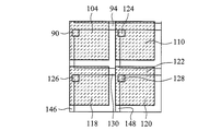
引き続き、図4aと図5を参照すると、画素電極、または、容量性プレート104がTFT90上に形成される。画素電極104は、フレキシブル基板73にほぼ平行に延伸し、ユーザーが指先を押し付ける表面に平行である。画素電極104は、画素電極104と、ゲート電極92及びロウライン94とを電気的に絶縁する層間絶縁層106の最上面でサポートされる。ビア108が、ゲート絶縁層102と層間絶縁層106を貫いて形成されて、画素電極104を、TFT90のドレイン電極96に電気的に接続する。図3bに示されるように、指紋センサー70の製造が完了するとき、画素アレイ72の画素電極104、110、112、114と116は、保護層により分離されるユーザーの指先の真下に位置する。注意すべきことは、TFT90のソースラインとドレインラインは、画素電極104下に完全に位置し、ユーザーの指先34との重要な直接的な静電結合に関与せず、これにより、ロウラインまたはカラムラインを介して導入される浮遊信号は減少する、。上述のように製造されるとき、ロウラインはTFTのゲートに接続され、カラムラインはTFTのソースに接続される。各画素電極104は、各TFTのドレインからユーザーの指先に、キャパシタを形成する。
With continued reference to FIGS. 4 a and 5, a pixel electrode or
図3bは、画素アレイの共通のロウに位置する全画素電極104、110、112、114と116を示す図である。実際には、画素電極の多数のロウがある。図4bのグリッドレイアウトを参照すると、画素電極104と110は、Row1に互いに隣接して配置され、TFT90とTFT124両方のゲート電極はロウライン94に共通に接続される。二個の別の画素電極118と120が図4bに示され、次に続くロウに位置する。それぞれ、画素電極118と120に関連するTFT126と128は、画素アレイのRow2に対応するロウライン130に接続されるゲート電極を各々有する。各画素電極は、本質的に、ユーザーの指先と、画素電極とユーザーの指先を電気的に分離する保護誘電層とに沿って、キャパシタを形成する。ユーザーの指先に送信される信号は、各キャパシタにより、画素アレイ72に結合される。ユーザーの指先の山がちょうど画素上にあるとき、この有効なキャパシタのプレートは互いにより近接し、ユーザーの指先の谷がちょうど、画素上にあるとき、この有効なキャパシタのプレートは、互いにより離れている。画素から画素へのこのようなキャパシタンスの変化のため、各画素のTFTにより結合される送信信号はそれに従って変化し、これらの変化は、指紋の像の形成に利用できる。このほか、材料スタックの上部近くに、大きい金属キャパシタまたは“画素電極”を形成するとともに、カラムラインをさらに下に位置させることにより、アレイ中の別の位置からの外部信号は、より効果的に、カラムラインにより検出されるデータから隔離される。その一方で、ICチップ86がフレキシブル基板73の底面に取り付けられて、ロウラインを駆動すると共に、カラムラインにより提供されるデータ信号を処理する。
FIG. 3b shows all
図4cは、指紋センサー70の簡潔な上面図である。画素アレイ72は、画素のXロウとYカラムを有し、各画素は、図4a、図4b、および、図5を参照して説明した方法で製造される。画素アレイ72は、送信リング74により周囲が囲まれて、高周波数信号をユーザーの指先に送信する。送信リング74は画素アレイ72の領域外側に位置する。送信リング74は、高周波数信号を効果的にユーザーの指先34に送信する。この放射信号は、ユーザーの指先により伝導され、指先表面の山と谷を通り抜け、顧客のシステム中の保護介在材料(すなわち、携帯電話カバーガラス)を通過し、画素アレイ72の容量性金属プレート、または、画素電極上で受信される。
FIG. 4 c is a simplified top view of
デマルチプレクサ140は、画素アレイ72の一方の側に沿って延伸する。デマルチプレクサ140は、、画素アレイ中のどのロウが任意の時点で選択されるかを示す制御信号をIC86から受信する。デマルチプレクサ140はその制御信号を復号すると共に、ロウライン(94、130,・・・142)を駆動して、その時々で一つのロウだけを有効にする。デマルチプレクサ140は、IC86と画素アレイ72の間で延伸する必要がある導電トレースの数を減少させる。たとえば、画素アレイ72が画素の256ロウを含む場合、画素アレイ72は256ロウラインを含む。一方、256ロウラインのひとつを選択するため、IC86とデマルチプレクサ140の間で延伸する8バイナリー制御ラインしか必要ない。
再度、図4bと図5を参照すると、カラム電極146、148、150と152を有する一連のYカラム電極が、画素アレイ72を貫いて延伸して、選択されたロウの対応するカラム中に位置する画素から生成された信号を検出する。たとえば、ロウ94が選択される場合、TFT90のソース電極に接続されるカラム電極146は、画素電極104により提供される信号を感知する。同様に、TFT124のソース電極に接続されるカラム電極148は、画素電極110により提供される信号を感知する。よって、各TFTのゲートが対応するロウドライバに接続され、各TFTのドレインが画素電極(ユーザーの指先とキャパシタを形成する)に接続され、および、各TFTのソース端子が、カラムライン、または、“データライン”に接続されて、信号処理のためのIC86に結合される。図示されるロウライン(94、130)とカラムライン(146、148、150と152)は、LCDの製造に用いられる透明金属であるインジウムスズ酸化物(ITO)を含む任意の導電金属から形成される。透明性が必要ないとき、その他の金属、たとえば、アルミニウム、または、銅を用いることもできる。
Referring again to FIGS. 4b and 5, a series of Y column electrodes having
図4cに戻ると、カラムデコード回路ブロック144が、図5に示されるカラム電極146、148、150と152を含む全カラム電極に電気的に接続される。よって、カラムデコード回路ブロック144は、選択されたロウ中の各画素で、信号レベルを検出する。画素アレイのXロウを順次選択することにより、ユーザーの指紋の像が、X×Y画素を有して生成される。検出された信号の特徴が、送信された信号がユーザーの指先の山または谷を経過するかどうかに基づいて変化する限り、容量性プレートまたは画素電極は、信号振幅、信号位相シフトまたは別の方法で、ユーザーの指先34から信号エネルギーを受信できる。必要に応じて、送信されたTx信号の特徴(周波数、振幅等)は、画素アレイからの一検出から次の検出に変更されてよいし、より正確なを生成するために、複数のサンプルを得て平均を求めてもよい。
Returning to FIG. 4c, the column
使用するとき、単一のロウドライバがオンになり、画素の特定のロウを起動する。送信リング74が用いられて、所定周波数で、既知の信号を送信する。選択されたロウ中の画素の信号コンテンツがカラムラインに転送されて、外部ICチップ86中で、検出、感知、および、処理される。このアプローチは、ICチップ86を、物理的に、画素アレイから離し、また、逆多重化/多重化スキームの使用により、ICチップ86と画素アレイの間のロウ選択ラインと感知された信号データラインの低減を可能にする。各画素電極(104、110等)は、指先とキャパシタを形成し、キャパシタの値は、各画素位置上の指(山または谷)表面によって決まる。各画素電極は、指先からの信号を受信し、および、関連するTFTが“ON”の場合(すなわち、この特定のロウのロウドライバが有効になり、このTFTの“ゲート”をオンにする)、容量性結合信号がTFTを通り、画素アレイの“データライン”、または、カラム電極に現れる。
In use, a single row driver is turned on and activates a particular row of pixels. A
カラムデコード回路ブロック144は、アレイの各画素で検出される信号を処理して、指紋の像を形成するIC86に電気的に接続される。カラムデコード回路ブロック144とICチップ86の間の導電トレースの数を最小化するため、検出された信号は、ブロックにして、カラムデコード回路ブロック144からICチップ86に送信される。たとえば、画素アレイ72が、画素の256カラムを有する場合、カラムデコード回路ブロック144は、一度に、16信号のブロックを送信し、それにはアレイの各ロウにつき16回の送信を必要とする。カラムデコード回路ブロック144とICチップ86の間の信号データ用の16本の導電トレース以外に、必要となるのは、16データブロック中のどれが送信されるかを示すためのわずか4本の別の制御ラインである。この多重化技術は、カラムデコード回路ブロック144とICチップ86の間で延伸させなければならない金属トレースの数を大幅に減少させる。
The column
図6は、デマルチプレクサ140、および、カラムデコード回路ブロック144が、IC86と画素アレイ72の間で延伸する必要がある導電トレースの数を減少させる方法を説明するのに役立つ。ロウライン94、130等は、デマルチプレクサ140により駆動される。デマルチプレクサ140は、ロウラインの数に等しい数の出力端子を有し、その時々で、一つのロウだけが選択される。対照的に、IC86とデマルチプレクサ140の間で延伸する選択ライン154の数は、指数関数的に減少する。再度、アレイに、画素の256ロウがある場合、選択ライン154は、256ロウの一つを一意に識別するために、たった8個の導電トレースを必要とする。このように、デマルチプレクサ140は、簡潔なデジタルロジックにより、(x)の選択ラインで2Xロウをアドレスする。あるいは、デマルチプレクサ140は、単に、デジタルシフトレジスタであって、ロジック“1”の出力信号は、Row1出力端子からRow2出力端子へ、という具合に連続的に渡され、全ロウが有効になるまで、一度に一ロウずつ有効にする。
FIG. 6 helps illustrate how
同様に、画素アレイが、カラム電極146、148、150と152を含む256カラム電極を有する場合、および、カラムが、さらに、16カラムの16ブロックに分割される場合、カラムデコード回路ブロック144は、図6のバス156で示される16個の導電トレースで、データの各ブロックを送信することができる。この例では、図6に選択ライン158として示される4個の別の導電トレースは、データの16ブロックのひとつを、一意的に画素の所定のロウにアドレスするのに十分である。カラムドライバの場合、信号はアナログで、アナログマルチプレクサにより、逆多重化しなければならない。例として、Y選択ラインを用いて、2Yカラムから一最終アナログ入力“M”を得る。この構成によれば、Mは、1、または、それより大きい数である。これは、単に、このプロセスに許容される必要な信号の減少、および、タイミングに基づく。たとえば、システムが、一度に単一の画素をアドレスする(M=1)ことを選択する場合、X×Y画素のすべてに、個別にアドレスされなければならない。
Similarly, if the pixel array has 256 column electrodes including
図7aは、画素アレイ72に関連するTx送信リング74’の位置を示す。Tx送信リング74’は簡潔な金属構造で、ゲート絶縁層102の上(図4aを参照)、または、ゲート絶縁層102の下方に形成される。Tx送信リング74’は、ICチップ86、または、外部ドライバにより供給される信号で駆動される。Tx送信リング74’は、画素アレイ72から十分離れて設置されて、送信リング74'から画素電極への直接の信号の入射を回避する;もっと正確に言えば、送信リング74'から放射される高周波数信号は、画素電極に結合される前に、まず、ユーザーの指先34を通過しなければならない。図7aにおいて、コネクタ160は、画素アレイ72とICチップ86の間で延伸して、電気信号を通過させる。必要であれば、図7bに示されるように、コネクタ160は、着脱可能なコネクタ160’として形成される。
FIG. 7 a shows the position of the Tx transmit
図8は、すでに記述された図3aに類似し、どのようにして、送信電極74と76により放射される信号が、ユーザーの指の層を介してユーザーの指先の山と谷に戻り、画素アレイに伝わるかを説明する。図8において、ユーザーの指先は、符号170により示される。山と谷を含むユーザーの指先の外層は、172により示される。外層172の真上は、組織174の内部導電層である。送信電極74と76から放射される高周波数信号は、それぞれ、矢印82と84に沿って上に通過し、保護誘電層78を経て、ユーザーの指先の外層172を経て、組織174の導電層に達する。層174により伝導する信号は、画素アレイ72に向かって下に放射され、外層172の山と谷を経て、さらに、矢印176により示される経路に沿って保護誘電層78を経て、画素電極(図8の178で示される)により受信される。図8において、画素アレイ72の下に設置される金属層180は、たとえば、画素アレイ中で、アクティブロウを選択するのに用いられるロウアドレスラインのルーティングを表す。再度、ICチップ86が、画素アレイ72をサポートする基板底面に取り付けられる。
FIG. 8 is similar to previously described FIG. 3a, in which the signal emitted by the transmit
図9において、本発明の別の実施態様がブロック図で説明され、送信電極は、画素アレイのロウアドレッシング電極間に組み込まれている。この例において、画素アレイ72は、96ロウと96カラムのマトリクスである。前述の実施態様のように、画素アレイ72は画素セルのマトリクスにより形成され、各画素セルは、TFTと画素電極を含む。図9において、ブロック190は、ロウライン192(row G0)、194(row G1)から196(row G95)をアドレスするのに用いられるロジックを表している。ロウライン192(G0)は、共通の第一ロウ中に位置するTFTのゲート電極に接続される(注意すべきことは、図9において、アレイは90度回転されており、ロウは、図の上下に延伸していることである)。同様に、ロウライン194(G1)は、共通の第二ロウに位置するTFTのゲート電極に接続される。ロウライン196(G95)は、画素アレイ72の共通の最終ロウに位置するTFTのゲート電極に結合される。
In FIG. 9, another embodiment of the present invention is illustrated in a block diagram, where the transmit electrodes are incorporated between the row addressing electrodes of the pixel array. In this example, the
前述の実施態様の場合のように、画素のアドレスされたロウ中の画素電極により受信される信号を感知するため、ライン198(C0)、200(C1)から202(C95)を含むカラムまたはデータ電極が、共通のカラムに沿って位置するTFTのソース端子に接続される。カラム電極ライン198(C0)、200(C1)から202(C95)は、それぞれ、カラムデコード回路ブロック144に接続されて、画素の選択されたロウ中の各画素電極により受信される信号を検出する。 As in the previous embodiment, a column or data containing lines 198 (C0), 200 (C1) to 202 (C95) to sense signals received by the pixel electrodes in the addressed row of pixels. An electrode is connected to the source terminal of the TFT located along a common column. Column electrode lines 198 (C0), 200 (C1) to 202 (C95) are each connected to a column decode circuit block 144 to detect signals received by each pixel electrode in a selected row of pixels. .
図9に示される実施態様中、TX0ライン204、TX1ライン、・・・、TX10ライン206からTX95ライン208を含み、TFTロウロジックブロック190から延伸し、および、ロウアドレッシングライン192(row G0)、194(row G1)から196(row G95)間に交互に配置されて延伸する一連の送信電極がある。図7aに示される送信リング74’の代わりに、これらのTXラインが用いられ、高周波数信号をユーザーの指先に送信する。まず、これは、送信電極を、画素アレイから横方向に隔てた状態にし、送信電極から画素電極への直接的な静電結合を防止する(すなわち、ユーザーの指先を迂回する)出願人の目的と相反するように見える。しかし、どの送信電極がその時々でアクティブであるかを慎重に選択すること、および、アクティブ送信電極と画素アレイの選択されたロウの間の距離を維持することにより、送信電極から画素電極への直接的な静電結合を概ね防止することができる。このほか、画素アレイの周辺ではなく、その中に送信電極を設置することにより、画素アレイの周囲を囲う送信電極のための追加領域を基板上に確保する必要性を無くせる。
In the embodiment shown in FIG. 9,
図10は、TFTロウロジックブロック190中に形成されるロジックコンポーネンツの高レベル機能図である。ロジックコンポーネンツは、ロウアドレッシングライン192(row G0)、194(row G1)から196(row G95)、および、TX0ライン204、TX1ライン206、・・・、TX10ライン207からTX95ライン208を制御するのに用いられる駆動信号を生成する。TFTロウロジックブロック190の動作は、図12に示されるタイミング波形を参照することによりさらに理解できる。ICチップ86は、開始信号220をTFTロウロジックブロック190に送信して、画素アレイ72の読み取り周期を開始し、ロジック素子をクリア/リセットする。パルスクロック信号222は、さらに、ICチップ86により、TFTロウロジックブロック190に提供されて、時間基準を提供する。ICチップ86は、さらに、ライン224で、パルスGDを送信して、ロウアドレッシングラインを有効にする手順の開始を指示する。パルスGDがアクティブである最初のクロックサイクルCで、ロウアドレスライン192(G0)がアクティブになり、画素の第一ロウ中のTFTのゲート電極を有効にする。次に続くクロックサイクルCで、ロウアドレスライン192(G0)はローレベルに戻り、次のロウアドレスライン194(G1)がアクティブになる。このプロセスは、96番目のクロックサイクルまで続き、ロウアドレスライン196(G95)がアクティブになる。
FIG. 10 is a high level functional diagram of the logic components formed in the TFT
引き続き、図9、図10、および、図12を参照すると、TX信号226は、ユーザーの指先に送信される高周波数信号を表している。上述のように、 TX信号226は、ICチップ86により、または、外部ソースから提供される。更なる信号TDが、第一フリップフロップレジスタ230への入力としてライン228に提供される。フリップフロップレジスタ230の出力はANDゲート232に結合される。フリップフロップレジスタ230の出力がローレベルのとき、ANDゲート232は、ライン226上の信号TXが、TX0ライン204に送信されるのを阻止する。フリップフロップレジスタ230の出力は、さらに、次に続くフリップフロップレジスタへのデータ入力として機能し、次に続くフリップフロップレジスタは、同様に、TX1ライン206等を駆動するANDゲートを制御する。
With continued reference to FIGS. 9, 10, and 12, the TX signal 226 represents a high frequency signal transmitted to the user's fingertip. As described above, the TX signal 226 is provided by the
図9と図10に関して、出願人は、その時々に感知される画素アレイのアクティブロウの両側に、約10ロウの非アクティブトランスミッタライン持たせれば十分であると判断した。よって、画素の第一ロウがゲート電極192により選択される場合、最初の10個の送信電極204(TX0)、206(TX1)、・・・TX9を無効にすることが望まれる。はじめに、第一フリップフロップ230を含む最初の11個のフリップフロップは、初期化(I)信号220によりリセットされ、残りのフリップフロップは初期化(I)信号220により設定される。よって、画素の第一ロウが選択されるとき、最初の11個の送信電極204(TX0)、206(TX1),・・・TX10は、それぞれのANDゲート(ANDゲート232を含む)により無効にされ、最初は、TX11からTX95の全部で85のアクティブ送信電極用に有効にされる。
With respect to FIGS. 9 and 10, Applicants have determined that it is sufficient to have about 10 rows of inactive transmitter lines on either side of the active row of the pixel array sensed from time to time. Therefore, when the first row of pixels is selected by the
各後続のクロックサイクルにおいて、アクティブ送信電極の数が76に減少するまで、別の送信電極が無効になる。クロック信号222(C)の最初の10クロックサイクル期間中、ICチップ86により提供されるTD入力信号228が、ロジックローレベル(“0”)に維持されて、それらのそれぞれのANDゲートにより無効になる最初の11個の送信電極204(TX0)、206(TX1)、・・・からTX10を維持し、右側の追加の送信電極が無効になる。10個のクロックサイクル後、TD入力信号228がロジックハイレベル(“1”)に切り替わり、画素の各ロウの読み取りを終了するのに用いられるクロックサイクルの剰余の間高いままを維持する。よって、画素の第11ロウがロウアドレスラインG10により選択されるとき、送信電極204(TX0)が有効になり、高周波数信号をユーザーの指に送信する一方、隣接する送信電極TX1からTX20は無効になる。このパターンは各クロックサイクルで継続され、効果的に、感知される選択されたロウの両側に、10個の非アクティブTXロウを提供する。アクティブ感知ロウが、各クロックサイクルで、画素アレイを横切るに従い、TX送信電極の"非アクティブ範囲"を与える。最後の20ロウが感知のために選択されるとき、非アクティブ送信電極の数は、20から10に減少し始める。この事例では、どの時点においても無効であるTX送信電極の最大数は20であり、少なくとも76個の別のTX送信電極が同時に有効になり、確実に、高周波数TX信号をユーザーの指に送信する。
In each subsequent clock cycle, another transmit electrode is disabled until the number of active transmit electrodes is reduced to 76. During the first 10 clock cycles of the clock signal 222 (C), the
図12に示されるように、ロウアドレスライン192(G0)が選択される期間、送信ライン204(TX0)、206(TX1)から207(TX10)はローレベルのままか、または、無効になる。一方、送信ライン234(TX11)から208(TX95)は、能動的に、高周波数TX信号で駆動されて、TX信号をユーザーの指先に送信するのを助ける。同様に、ロウアドレスライン/ゲート電極G10が選択されるとき、TX1からTX10、および、TX11からTX20の送信電極は無効になり、他のTXライン(すなわち、TX0とTX21−TX95)は全て有効になり、TX信号をユーザーの指先に送信するのを助ける。このように、感知中の画素電極は、隣接するTXラインから直接、送信されたTX信号を受信しないが、画素電極とユーザーの指先の間の容量結合の結果としてのみ受信する。さらに、図10に示されるTFTロウロジックブロック190の全ロジック回路は、画素アレイを形成するのに用いられるのと同一種類のTFTを用いて、画素アレイ72が形成される同一フレキシブル基板上に形成される。
As shown in FIG. 12, during the period when the row address line 192 (G0) is selected, the transmission lines 204 (TX0), 206 (TX1) to 207 (TX10) remain at a low level or become invalid. On the other hand, transmission lines 234 (TX11) to 208 (TX95) are actively driven with a high frequency TX signal to help transmit the TX signal to the user's fingertips. Similarly, when the row address line / gate electrode G10 is selected, the TX1 to TX10 and TX11 to TX20 transmit electrodes are disabled, and the other TX lines (ie, TX0 and TX21-TX95) are all enabled. It helps to send the TX signal to the user's fingertip. Thus, the sensing pixel electrode does not receive the transmitted TX signal directly from the adjacent TX line, but only as a result of capacitive coupling between the pixel electrode and the user's fingertip. Furthermore, all the logic circuits of the TFT
図11と図12の波形図は、カラムデコード回路144(図9と図10を参照)がマルチプレクサとして構成され、画素アレイ72とICチップ86の間を走る導電線の数を減少させる方法を説明する。バス250により表される3個のバイナリー選択信号は、ライン254から256を含む8出力ラインを提供する3−to−8デコーダ252により受信される。破線ボックス258で示される第一マルチプレクサは、一連の8TFTを有する。最初のTFTが、カラム電極260(c95)と出力ポート264(Cout11)の間に介在する。破線ボックス258中の最後のTFTは、カラム電極262(c88)と出力ポート264(Cout11)の間に介在する。よって、8個のカラム電極c95からc88の一つが、その時々において出力ポートCout11に結合される。
11 and 12 illustrate how the column decode circuit 144 (see FIGS. 9 and 10) is configured as a multiplexer to reduce the number of conductive lines running between the
引き続き、図11を参照すると、266と268で示されるものを含む11以上のマルチプレクサが提供され、同じ方法で、出力ポート270(Cout0)から272(Cout10)にデータ信号を提供する。よって、12個の出力信号は、その時々において出力ポート270から264(Cout0からCout11)により提供される。8個の可能な状態のそれぞれの間中、選択バス信号250を循環させることにより、データの全96カラムが感知されると共に、ICチップ86に伝導される。図12に示されるように、各ロウアドレ期間中、8個の可能な状態を通して、選択バス信号250が循環されて、選択されたロウ中の全カラムが感知される。よって、図12において、選択バス信号250が第一状態(=0)であるとき、カラムc0が感知され、ユーザーの指先の山または谷が対応する画素電極上にあるかどうかに基づいて、送信されたTX信号波形がライン198(c0)上により大きい、またはより小さい程度に再現される。同様に、選択バス信号250が第二状態(=1)であるとき、ユーザーの指先の山または谷が対応する画素電極上にあるかどうかに基づいて、カラムc1が感知され、送信されたTX信号波形がライン200(c1)上に、より大きい、またはより小さい程度に再現される。
Continuing to refer to FIG. 11, 11 or more multiplexers, including those shown at 266 and 268, are provided and provide data signals to output ports 270 (Cout0) to 272 (Cout10) in the same manner. Thus, twelve output signals are provided by
当業者ならわかるように、上述の指紋センサーは、タッチスクリーンモニターを有するコンピュータ、タブレット型コンピュータ、または、携帯電話に用いられるタイプの従来のLCDタッチパッド中に組み込まれる。たとえば、図13は、図3から図8と併せて記述された、画素アレイ304を囲む送信電極リング302を含む一般型の指紋センサー300を示す図である。図14を参照すると、携帯電話LCDタッチパッドディスプレイパネル310は、その左下隅に、図13の指紋センサー300が組み込こまれている。
As will be appreciated by those skilled in the art, the fingerprint sensor described above is incorporated into a conventional LCD touchpad of the type used in computers with touch screen monitors, tablet computers, or cell phones. For example, FIG. 13 is a diagram illustrating a
一般のLCDタッチパッドにおいて、すなわち、指紋センサー領域300の外側に位置する図14のパネル310の部分は、約500ミクロンのピッチで配置される比較的低密度の画素の二次元アレイで形成される。すなわち、ある画素セルの中央から隣の画素セルの中央までの距離は約500ミクロンである。パネルは、単に、指先、または、タッチペンがディスプレイパネル310の領域に接触していることを検出する必要があるだけなので、画素密度は比較的低い。対照的に、正常に機能させるため、指紋センサーアレイ部分300は、中央から中央まで約50−70ミクロンのより微細なピッチで配列されたより高密度の画素を有すべきである。よって、指紋センサー領域300には、タッチパッドパネル310中、画素ロウ毎に10ロウもの画素がある。同様に、指紋センサー領域300には、タッチパッドパネル310中、画素カラム毎に10カラムもの画素がある。
In a typical LCD touchpad, i.e., the portion of
しかし、指紋センサー領域300の製造に用いられる技術は、ディスプレイパネル310の剰余により、低密度のタッチセンサー画素を製造するのに用いられる技術と非常に類似する。よって、図14に示される指紋センサー領域300は、ディスプレイパネル310左下隅に制限されるが、必要に応じて、指紋センサー領域300を拡大して、ディスプレイパネル310の底面全体を被覆したり、または、ディスプレイパネル310中の別の領域に拡大してもよいことが理解されなければならない。
However, the technology used to manufacture the
外部ノイズ信号をさらに防止するため、画素電極により検出される信号を感知する正確さは、差動モードで、画素電極信号を感知することによりさらに増加させることができる。このアプローチは、人体自身、または、別のソース、たとえば、指紋センサーが設置される電子装置に起因する全タイプのコモンモードノイズの除去を可能にする。図16を参照すると、TFT400とその関連する画素電極401は、指紋センサー領域の第一画素を形成する;TFT402とその関連する画素電極403は、TFT400で、同一ロウ中、第二画素を形成する;および、TFT404とその関連する画素電極405は、TFT400と同一カラム中、第三画素を形成する。TFT400とTFT402は、第一ロウアドレッシングライン406に接続される。TFT404は、第二ロウアドレッシングライン408に接続される。TFT400とTFT404のソース端子は、どちらも第一カラム電極410に接続される;TFT402のソース端子は、第二カラム電極412に接続される。
To further prevent external noise signals, the accuracy of sensing signals detected by the pixel electrodes can be further increased by sensing the pixel electrode signals in differential mode. This approach allows the removal of all types of common mode noise due to the human body itself or another source, for example the electronic device where the fingerprint sensor is installed. Referring to FIG. 16,
引き続き、図16を参照すると、第一カラム電極410が第一差動増幅器414の正(非反転)の入力端に接続される。同様に、第二カラム電極412が第二差動増幅器416の正(非反転)の入力端に接続される。一例として、以下に説明するように、差動増幅器の数は、カラム電極の数よりひとつ少ないことを除いて、同様の差動増幅器が画素アレイの残りのカラム電極に提供される。カラム電極418は、各差動増幅器414、416等の負の(反転)端子に接続される。カラム電極418は、通常のカラム電極410、412等と同じ程度まで広がり、画素アレイの長さだけ延在する。一般のカラム電極(すなわち、410と412)により受信される浮遊、干渉信号はさらに、カラム電極418により受信される。よって、差動増幅器414は、カラム電極410が作り出す信号からのカラム電極418が作り出す浮遊、干渉信号を効果的に取り去り、および、得られた出力信号420は、不要なノイズ成分がなく、選択された画素ロウ中の画素電極により感知される信号を含む。
Still referring to FIG. 16, the
図16において、必要であれば、カラム電極418は、実際には、アクティブ画素に結合されない“ダミー”電極である。人体ノイズの除去において、このダミーカラムは、実際のカラム電極と同様に、ユーザーの指に近接する領域に位置しなければならない。あるいは、カラム電極418は、アレイ中の画素の特定カラムに関連する実際のカラム電極である;この場合、コモンモードノイズを受信する“犠牲”であるカラム電極に感知されるデータは存在しない。画素アレイの欠測カラム用にデータ信号を再形成するため、指紋が任意データではないことに気づくべきである。本質的に、指紋は山(最大)と谷(最小)を有し、指紋像は、最小と最大信号の間で変動する。画素アレイの欠測カラムにおけるデータを再構成する比較的簡単な方法の一つは、周囲の画素の値を見て、欠測データ値を計算し、欠測カラムの各ロウ中の値を補間することである。
In FIG. 16, if necessary, the
図13と図14に関連して、上述されたように、指紋センサー領域300は、従来のLCDタッチパッドパネル310中に組み込まれる。さらに、従来のLCDタッチパッドパネルにおける指紋センサー領域300の統合に役立たせるため、指紋センサー領域300は、選択的に、周囲の低密度感知画素の動作を模倣するモードで動作する。
As described above in connection with FIGS. 13 and 14, the
図17aを参照すると、指紋センサー領域500は、タッチパッドディスプレイパネル502の左下隅中に形成される。この例において、図9−図12と共に記述される一般的な方法で動作する交互配置される送信電極を選択して、図13の周囲の送信リング302が省略される。タッチパッドディスプレイパネル502は、低密度感知画素504から520のアレイを有する。各感知画素504から520は、ユーザーの指先、または、タッチペンが、このような感知画素の直上のカバーガラスに当てられるかを検出する。図17aに示される例において、単一の低密度画素(すなわち、504)毎に、指紋センサー領域500中、線上に伸びる長さごとに、約7の高密度画素がある。指紋センサー領域500により占有される領域は、低密度画素の4×4アレイの領域を代替する。指紋センサー領域500が“指紋モード”で使用されて、指紋画像を生成するとき、画素アレイ中の各画素電極は、個別に、すでに述べた方法で、アドレスされ、および、感知される。
Referring to FIG. 17 a, the
図17bを参照すると、“模倣 モード”の動作期間中、指紋センサー領域500中の7×7画素のグループは、仮想低密度画素を形成するよう連動し、タッチパッドディスプレイパネル502の低密度画素504から520を模倣する。図17bに示されるように、仮想低密度画素522は、高密度画素の7×7アレイにより形成される。タッチパッド領域520を模倣するためにFPS領域500が構成されると、FPS領域500のロウは、連動モードで、選択され、または、選択されない。どの時点においても、有効にされる/選択されるFPS領域500中のロウ数は、密度タッチパッド画素のサイズに対する高密度FPS画素のサイズに基づく。図17aと図17bに示される例において、FPS領域500の7ロウのグループは連動する。7個の隣接するロウの選択のほか、同時に、7個の隣接するカラム電極が短絡する。このように、49画素 (7×7)の画素電極に集められた信号は平均化されて、タッチパッドディスプレイパネル502の各低密度画素(すなわち、504、506等)により生成される信号を模倣する一出力信号を提供する。当業者ならわかるように、この“模倣 モード”の動作において、必要に応じて、FPS領域500中の連動する/短絡したカラム電極とタッチパッドパネルの存在するカラムラインを結合させて、提供される信号を感知、および、処理することが望ましい。
Referring to FIG. 17b, during the “mimetic mode” operation period, the 7 × 7 pixel group in the
図18に示されるように、タッチパッドディスプレイパネル502は、4個の低密度画素503、504、505と506を有する。これらの低密度センサー画素は、ロウライン530と532、および、カラムライン534と536によりアドレスされる。図18において、指紋センサー領域の高密度画素は図示のように連動し、ここでは各低密度画素は、10画素×10画素の高密度画素に対応する。この例において、タッチパッド画素(503、504、505と506) は500μm×500μmであり、FPS画素は50μm×50μmである。FPS領域がタッチパッド領域を模倣するため、FPS Row1からFPS Row10は同時に“ON”になり、FPSカラムは、10カラムのグループ単位 (すなわち、FPSカラム1からFPSカラム10;FPSカラム11からFPSカラム20等)で短絡する。このように、仮想FPS画素サイズは、50μm×50μmから500μm500μmに増加する。複数のロウを同時に選択することによるFPSロウのグループ化と、必要数のカラムの短絡は、TFTを用いて完成する。この方法は、ファイン画素FPSが、タッチパッドの大きい画素を模倣するのを許容する。
As shown in FIG. 18, the
指紋センサー領域500の高密度画素は、ロウ選択ライン548によりアドレスされ、選択されたロウのカラムは、カラム電極ライン550により感知される。4個の仮想低密度画素は540、542、544、546で示される。指紋像が必要なとき、10個のロウアドレスライン(FPS Row11からFPS Row20)は、個別に、仮想低密度画素540中の10個のロウ (11−20)をアドレスする、または、低密度画素の動作を模倣するとき、10個すべてのロウは、同時に選択される。同様に、指紋画像が必要なとき、10個のカラム感知電極(FPSカラム1からFPSカラム10)は、個別に、仮想低密度画素540中の10個のカラム(1−10)を感知する、または、低密度画素の操作を模倣するとき、10個すべてのカラムが短絡する。
The high density pixels in the
図19のタイミング波形は、低密度画素の動作を模倣するのに用いられるときの指紋センサー領域 (FPS) 500、および、その高密度画素の動作をさらに説明する。第一クロックサイクル(t0)中、FPS Row1−10はすべて有効になり、仮想画素544と546が選択される。同一クロックサイクル中、FPSカラム1−10が短絡して、仮想画素544を感知し、FPSカラム11−20が短絡して、仮想画素546を感知する。次のクロックサイクル(t1)中、FPS Row1−10はすべて、もう一度無効になり、FPS Row11−20はすべて有効になり、仮想画素540と542が選択される。再度、クロックサイクルt1中、FPSカラム1−10が短絡して、仮想画素540を感知し、FPSカラム11−20が短絡して、仮想画素542を感知する。このプロセスは、全仮想画素が感知されるまで継続される。その後、ロウ530と532を含むタッチパッドパネル (すなわち、TP Row1;TP Row2;TP Row3; ... TP Row N)のロウが個別に選択される期間中、十分な数の追加クロックサイクルが続き、選択されたタッチパッドロウ中の画素が、ユーザーの指、または、タッチペンによりタッチされているか判断するためにタッチパッドカラムライン (すなわち、534と536)が感知される。
The timing waveforms of FIG. 19 further illustrate the operation of the fingerprint sensor area (FPS) 500 and its high density pixels when used to mimic the operation of low density pixels. During the first clock cycle (t0), FPS Rows 1-10 are all valid and
図14と図15bは、LCDタッチセンサーパネル、または、タッチパッドを示し、タッチパッドは、高密度TFT/容量性プレート画素アレイで形成されるが、通常、低密度タッチパッドモードで動作する。タッチパッドモードで動作するとき、高密度 (ファインピッチ)画素は、上述のような方式で、低密度タッチパッド画素の動作を模倣する。図15aと15bは、タッチパッドの動作方法を説明するのに役立ち、指紋センサー領域は、選択的に、ユーザーが指を当てるタッチパッドの位置で提供される。図15aにおいて、タッチパッド702は、隣接タッチパッド画素704と706を含む低密度タッチパッド画素のアレイを含む。図15aにおいて、ユーザーの指先が、“接触”領域、破線楕円形700により指定されるタッチパッドの領域に当てられる。
14 and 15b show an LCD touch sensor panel or touch pad, which is formed of a high density TFT / capacitive plate pixel array, but typically operates in a low density touch pad mode. When operating in touchpad mode, high density (fine pitch) pixels mimic the operation of low density touchpad pixels in the manner described above. FIGS. 15a and 15b help illustrate how the touchpad operates, and the fingerprint sensor area is optionally provided at the location of the touchpad where the user applies the finger. In FIG. 15a,
図15bは、タッチパッド702下半分の拡大図で、破線楕円形700は、タッチパッド画素704と706に対応する領域を有する破線楕円形700近くに位置するタッチパッド画素により形成されるタッチパッド702の長方形領域に重なる。しかし、図15bにおいて、タッチパッド画素704と706、および、破線楕円形700近くに位置する別のタッチパッド画素は、指紋センサーモードに切り替えられ、ファインピッチの高密度画素画素は、集合的ではなく、個別的に動作し、タッチパッド画素モードで動作するときよりも高い解像度を提供する。
FIG. 15 b is an enlarged view of the lower half of the
低密度タッチパッドを模倣するタッチパッド702は、タッチパネル領域全体、または、タッチパネル領域の一部を有効にして、指紋センサー領域として用いられる。必要であれば、指紋像が、タッチパネル702上の任意の位置から得られる。第一に、タッチパッド702は、アドレッシングロウを短絡させ、および、カラム感知ラインを短絡させることにより、従来のタッチパッドとして構成されて、上述のような大きくて、低密度の画素を形成することができる。第二に、タッチパネル702は、大きく、且つ、高解像度の指紋センサーとして用いられ、一本の指、複数の指、または、手のひら部分を感知することができる。最後に、タッチパネル702は、タッチパッドとして構成されて、まず、人の指先が位置する場所を検出し、その後、指先位置に基づいて、検出された位置を指紋センサー領域として構成し、人の指紋を撮像する。
A
タッチパネル702が、タッチパッドとして用いられようと、指紋センサー領域として用いられようと、ユーザーが当てる指の位置は検出される。タッチパネル702が、従来のタッチパッドの動作を模倣するとき、従来のタッチパッドで指の位置および指のスワイプ方向を判断するために使用されるのと同じ方法が、同じ目的で、タッチパネル702にも用いられる。指先の位置が検出されると、間近の周辺領域が高解像度指紋センサー領域に切り替わり、指紋の高品質像をキャプチャする。
Whether the
図15aと15bに示される方法の実施において、ファインピッチ画素のアレイは、タッチパネル702の表面全体にわたって交差するロウとカラムに沿って配列される。前に述べたように、各ファインピッチ画素は、好ましくは、スイッチング装置 (すなわち、TFT)と容量性プレートを有し、ユーザーの指を介して送信される高周波数信号を感知する。一連のファインピッチロウアドレスラインが備えられ、それぞれ、アレイ中のファインピッチ画素のロウと関連付けられる。各ファインピッチロウアドレスラインは、アレイの対応するロウに関連付けられたファインピッチ画素を選択的にアドレスすることができる。前述同様、複数のファインピッチカラム感知ラインも備えられ、各ファインピッチカラム感知ラインは、ファインピッチ画素アレイ中のファインピッチ画素のカラムと関連付けられる。各ファインピッチカラム感知ラインは、ファインピッチ画素アレイの選択されたロウにおけるファインピッチ画素の容量性プレートにより提供される信号を感知することができる。図15a及び図15bには示されないが、当業者ならわかるように、図9と図10に関連して上述したような高周波数信号トランスミッタ電極が画素アレイ中に含まれ、選択的に、有効と無効にされて、効果的に、高周波数信号を、タッチパッド702の“接触” 領域に当てられるユーザーの指先に伝える。
In the implementation of the method shown in FIGS. 15 a and 15 b, the array of fine pitch pixels is arranged along rows and columns that intersect across the entire surface of the
図17a、図17b、および、図18に関して上述で示されるように、ファインピッチ画素は、図15b中のタッチパッド画素704と706のように、大きいタッチパッド画素のアレイにグループ化、または、細く分割され、さらに、ロウとカラムに配列される。タッチパッド画素のアレイは、基礎となる同一の二次元空間を被覆するが、より少ないロウとカラムを含むという意味で、“小さいアレイ”である。各タッチパッド画素は、ファインピッチ画素の少なくとも二つ、典型的には、5個以上の異なるロウ中に位置するファインピッチ画素を有する。同様に、各タッチパッド画素は、ファインピッチ画素の少なくとも二つ、典型的には、5個以上の異なるカラム中に位置するファインピッチ画素を有する。あるタッチパッド画素と隣接するタッチパッド画素の中心間距離は、あるファインピッチ画素と隣接するファインピッチ画素の中心間距離の少なくとも二倍の大きさで、より典型的には、5倍以上大きい。
As shown above with respect to FIGS. 17a, 17b and 18, the fine pitch pixels are grouped or thinned into an array of large touchpad pixels, such as
引き続き、図15aと図15bを参照すると、上述の方法は、第一モードの動作を含み、タッチパッド702中の全ファインピッチ画素が、704と706のように、低密度タッチパッド画素の動作を模倣するように構成される。この第一モードの動作において、たとえば、タッチパッド画素704を集合的に形成するファインピッチ画素は、集合的な動作のため同時に有効にされる。つまり、タッチパッド画素704中に位置するファインピッチ画素の全ロウアドレスラインが同時に有効になる (すなわち、そのファインピッチ画素のグループを有効にするロウアドレッシングラインが事実上互いに短絡する)。同様に、タッチパッド画素704中に位置するファインピッチ画素に接続されるカラム感知電極も実質的に短絡して、集合的に、タッチパッド画素704中に位置する全ファインピッチ画素の容量性プレートにより提供される信号を感知する。このように、第一モードの動作期間中、各タッチパッド画素は、従来のタッチパッドの従来のタッチパッド画素の機能を模倣する。このような第一モードの動作期間中、タッチパッド画素により提供される信号は、ポインタ(指先、タッチペン等)が、タッチパッド702上面に近接して当てられているかを検出するのに用いられ、検出した場合、タッチパッド702上のこのようなポインタの位置も検出される。
Continuing with reference to FIGS. 15a and 15b, the method described above includes a first mode of operation where all fine pitch pixels in
図15bを参照すると、たとえば、ユーザーの指先の像が撮像されるとき、タッチパッド702は第二モードの動作に変化する。この第二モードの動作期間中、どのタッチパッド画素が、ポインタ位置近くに位置するか判断される。たとえば、図15bにおいて、ポインタ位置に近接する20個のタッチパッド画素のグループ(4個のタッチパッド画素幅、5個のタッチパッド画素高さ)が判断される;それら20タッチパッド画素の中に、図15a中に704と706で示されるものがある。20個のタッチパッド画素は、その後、再設定され、すなわち、選択的に切り替えられ、個別に、アドレス、および、感知されるファインピッチ画素に戻される。この個別モードの動作期間中、各ファインピッチロウ中のファインピッチ画素は、個別に有効になり、各ファインピッチロウが、対応するファインピッチロウアドレスラインにより有効になるとき、各ファインピッチ画素の各容量性プレートにより提供される信号が個別に感知される。このような理由で、図15bにおいて、“接触”領域700中で示されるアレイまたはグリッドは、“接触”領域700の外側に位置するタッチパッド画素よりさらに密に描かれている。したがって、このとき“接触”領域700中の個々のファインピッチ画素は、ユーザーの指先の指紋画像を感知するための指紋センサー領域を形成するように構成されている。
Referring to FIG. 15b, for example, when an image of the user's fingertip is captured, the
図15aと図15bは、タッチパッド702が、タッチパネル702中のどこであっても、ユーザーの指により現在タッチされている接触領域に近接する指紋センサー領域を提供することを示す。しかし、当業者なら理解できるように、必要に応じて、指紋センサー領域は、タッチパッド702の全体表面を覆うように拡大できる。つまり、図15aに示されるすべてのタッチパッド画素は、第一(または“模倣”)モードの動作から第二(または“個別”)モードの動作に切り替えることができ、タッチパッド表面全体が、高密度画素モードで動作するようになる。このように、二個以上の指紋、または、掌紋でさえ、その像をを感知できる。
FIGS. 15a and 15b illustrate that the
図20aと図20bに示されるように、上述の指紋センサーは、さらに、ボタンに組み込まれる。ボタン600は、たとえば、保護されたドアやエレベータ等のセキュリティ機能で、進入許可は、指紋が、すでに保存されている指紋に符合するユーザーだけに制限され、その身分は、予め、認証されている。ボタン600は、ガラス604の保護層により被覆される画素アレイ602を有する。画素アレイは、接着剤609により、プリント回路板608に装着されるフレキシブル基板606上に形成される。集積回路チップ686は、プリント回路板608に取り付けられる。フレキシブルな電子コネクタ610は、フレキシブル基板606とプリント回路板608の間で延伸し、画素アレイ602とICチップ686の間の電気的接続を形成する。図20aにおいて、周囲のリング612が備えられ、ユーザーが指でボタンを押すとき、高周波数信号をユーザーの指に送信する。あるいは、必要に応じて、外部送信電極が省略され、すでに記述された方式で、定められた時点で感知される特定のロウから離れて、送信電極が選択的に活性化される。
As shown in FIGS. 20a and 20b, the fingerprint sensor described above is further incorporated into the button. The
当業者ならわかるように、記述される指紋センサーは、タッチ電子工学の利用に役立ち、下に位置する画素アレイのより強固な保護を提供する厚い保護面を通して指紋像を読み取るセンサーの能力を向上させる。よって、たとえば、 本発明の指紋センサーは、携帯電話タッチディスプレイパネル中によく提供される厚いカバーガラスとうまく利用できる。このほか、記述される装置は、画素アレイのサイズとは無関係に、比較的小さい集積回路チップと共に利用され、製造コストを減少させる。開示された指紋センサーは、信号強度を増加し、厚い材料を介した信号対ノイズ比を改善し、厚い材料を介した信号“集中”を維持する能力を提供して、それにより指の山と谷の像が、適切に検出され、十分に高い解像度を持つ。本発明は、携帯電話、タッチパッド、ノートパソコン、ノートパッド、電子ブック等のタッチセンサー表面を用いるアプリケーションに用いられる。本発明は、バイオメトリックスセキュリティを、電子製品中に組み込むのに用いられ、製品サイズ、コスト、処理への影響が最小限である。 As will be appreciated by those skilled in the art, the described fingerprint sensor helps in the utilization of touch electronics and improves the sensor's ability to read fingerprint images through a thick protective surface that provides stronger protection of the underlying pixel array. . Thus, for example, the fingerprint sensor of the present invention can be successfully used with the thick cover glass often provided in mobile phone touch display panels. In addition, the described device is utilized with relatively small integrated circuit chips, regardless of the size of the pixel array, reducing manufacturing costs. The disclosed fingerprint sensor provides the ability to increase signal strength, improve signal-to-noise ratio through thick material, and maintain signal “concentration” through thick material, thereby reducing finger crests Valley images are properly detected and have sufficiently high resolution. The present invention is used for an application using a touch sensor surface such as a mobile phone, a touch pad, a notebook computer, a note pad, and an electronic book. The present invention is used to incorporate biometric security into electronic products with minimal impact on product size, cost, and processing.
好ましい実施態様の記述からわかるように、本発明は、指紋センサーを提供し、指紋の像をキャプチャするのに用いられる画素アレイと同じサイズの集積回路半導体チップを使用しなくても、人の指紋を撮像することができる。これにより、生産費を大幅に減少させる。本発明の指紋センサーは、画素アレイを覆うカバープレートに当てられる指先の山と谷を、それが相対的に厚いカバープレートであっても、より容易に識別する。本発明は、高周波数キャリア信号を、同時に直接画素アレイに結合することなく、効果的に人の指先に送信する。すなわち、キャリア信号は、画素アレイに送り戻される前に、ユーザーの指先を通過するように集中させられる。 As can be seen from the description of the preferred embodiment, the present invention provides a fingerprint sensor, and without using an integrated circuit semiconductor chip of the same size as the pixel array used to capture the fingerprint image, Can be imaged. This greatly reduces production costs. The fingerprint sensor of the present invention more easily identifies the peak and valley of the fingertip applied to the cover plate that covers the pixel array, even if it is a relatively thick cover plate. The present invention effectively transmits a high frequency carrier signal to a human fingertip without simultaneously coupling it directly to the pixel array. That is, the carrier signal is concentrated to pass through the user's fingertip before being sent back to the pixel array.
上で述べたように、本発明に基づいて構成される指紋センサーは、さらに、画素アレイによりキャプチャされる指紋像を処理するのに用いられる画素アレイと関連する集積回路との間で延伸しなければならない伝送線の数を大幅に減少させる。これは、その大部分が、ロウアドレスラインを逆多重化することにより、および/または、カラムデータラインを多重化することによる。本発明は、画素電極により検出される信号の差動感知に役立ち、コモンモードノイズ信号の拒絶を改善する。本発明の指紋センサーは、容易に、従来のタッチセンサーパッドに組み込むことができ、指紋のイメージの形成に用いられないとき、同じ感知層と同じ製造技術を用いて、タッチパッドの低密度画素を模倣することもできる。 As noted above, a fingerprint sensor constructed in accordance with the present invention must further extend between the pixel array used to process the fingerprint image captured by the pixel array and the associated integrated circuit. The number of transmission lines that must be reduced is greatly reduced. This is largely due to demultiplexing row address lines and / or multiplexing column data lines. The present invention helps differential sensing of the signals detected by the pixel electrodes and improves rejection of common mode noise signals. The fingerprint sensor of the present invention can be easily incorporated into a conventional touch sensor pad, and when not used to form a fingerprint image, using the same sensing layer and the same manufacturing technology, the low density pixels of the touch pad are used. It can also be imitated.
本発明について好ましい実施態様に関して説明したが、これらは決して本発明を限定するものではなく、当該技術を熟知する者なら誰でも、本発明の精神と範囲を脱しない範囲内で各種の変形や変更を加えることができ、従って本発明の保護範囲は、特許請求の範囲で規定した内容を基準とする。 Although the present invention has been described with reference to preferred embodiments, they are not intended to limit the invention in any way, and any person skilled in the art may make various modifications and changes without departing from the spirit and scope of the invention. Therefore, the protection scope of the present invention is based on what is defined in the claims.
30 従来の指紋センサー
32 シリコンチップ
34 ユーザーの指先
36 指先の山
38 指先の谷
40 画素
50 既知の指紋センサー
52 Xロウ
54 Yカラム
58 ICチップ
60 追加金属トレース
70 指紋センサー
72 画素アレイ
73 フレキシブル基板
74,76 Tx送信トレース
74’ 送信リング
78 保護誘電層
80 最上面
86 集積回路シリコンチップ
90 TFT
92 ゲート電極
94 ロウアドレスライン
96 ドレイン電極
98 ソース電極
100 半導体領域 102 ゲート層
106 層間絶縁層
108 ビア
104,110,112,114,116,118,120 画素電極
126,128 TFT
130 ロウライン
140 デマルチプレクサ
144 カラムデコード回路ブロック
146,148,150,152 カラム電極
156 バス
158 選択ライン
160 コネクタ
160’ 着脱可能なコネクタ
172 外層
174 層
180 金属層
190 TFTロウロジックブロック
192 ロウライン(row G0)
194 ロウライン(row G1)
196 ロウライン(row G95)
198 カラム電極ライン
204 送信電極
220 初期化(I)信号
222 クロック信号
226 TX信号
228 TD入力信号
230 第一フリップフロップレジスタ
232 ANDゲート
250 バス
252 デコーダ
260 カラム電極
264 出力ポート
262 カラム電極
270 出力ポート
300 指紋センサー
302 送信電極リング
304 画素アレイ
310 携帯電話LCDタッチパッドディスプレイパネル
400,402 TFT
406 第一ロウアドレッシングライン
408 第二ロウアドレッシングライン
410 第一カラム電極
414 第一差動増幅器
412 第二カラム電極
416 第二差動増幅器
418 カラム電極
420 得られた出力信号
500 指紋センサー領域
502 タッチパッドディスプレイパネル
504 感知画素
530,532 ロウライン
534,536 カラムライン
540,542,544,546 低密度感知画素
548 ロウ選択ライン
550 カラム電極ライン
600 ボタン
602 画素アレイ
604 ガラス
606 フレキシブル基板
608 プリント回路板
686 集積回路チップ
609 接着剤
610 フレキシブルな電子コネクタ
612 周囲のリング
702 タッチパッド
704,706 隣接タッチパッド画素
30
92
130
194 Row G1
196 row line (row G95)
198
406 First
Claims (24)
a)複数の画素を有し、上面を含み、前記複数の画素がRロウとNカラムの画素アレイに配列され、各画素がスイッチング装置を有し、さらに、前記上面に近接する容量性プレートを有する第一基板と、
b)前記画素アレイの対応するロウ中の前記画素の前記スイッチング装置に接続され、選択的に、前記対応する画素ロウ中の前記スイッチング装置を有効にする複数のRロウアドレッシング電極と、
c)前記画素アレイの対応するカラム中の前記画素の前記スイッチング装置に接続されて、前記画素アレイの選択されたロウと前記対応するカラムの交差点に位置する前記画素の前記容量性プレートにより提供される信号を感知する複数のNデータ電極と、
d)前記第一基板の前記上面を被覆し、ユーザーの指先を受けるカバー層と、
e)前記第一基板の前記上面に近接して形成されると共に、横方向に、前記画素アレイから隔てられて、電気信号を送信する少なくともひとつのトランスミッタ電極と、を有し、
f)少なくともひとつのトランスミッタ電極により送信される前記電気信号が、前記カバー層に当てられるユーザーの指に結合され、前記ユーザーの指先の山または谷が、前記画素アレイ中の特定の画素を覆うかどうかに基づいて、前記ユーザーの指に連結される前記電気信号は、さらに、前記画素アレイ中の前記容量性プレートにより、より大きいか、または、より小さい程度に結合されることを特徴とする指紋センサー。 A fingerprint sensor composed of a combination,
a) having a plurality of pixels, including a top surface, the plurality of pixels being arranged in a pixel array of R rows and N columns, each pixel having a switching device, and further comprising a capacitive plate close to the top surface A first substrate having,
b) a plurality of R row addressing electrodes connected to the switching device of the pixel in the corresponding row of the pixel array and selectively enabling the switching device in the corresponding pixel row;
c) provided by the capacitive plate of the pixel located at the intersection of the selected row of the pixel array and the corresponding column connected to the switching device of the pixel in the corresponding column of the pixel array. A plurality of N data electrodes for sensing signals,
d) a cover layer that covers the top surface of the first substrate and receives a fingertip of a user;
e) at least one transmitter electrode formed adjacent to the top surface of the first substrate and laterally spaced from the pixel array for transmitting an electrical signal;
f) whether the electrical signal transmitted by at least one transmitter electrode is coupled to a user's finger applied to the cover layer, such that a peak or valley of the user's fingertip covers a particular pixel in the pixel array; And the electrical signal coupled to the user's finger is further coupled to a greater or lesser extent by the capacitive plate in the pixel array. sensor.
a)上面を有する基板と、
b)前記基板中に形成されると共に、交差するロウとカラムに沿って配置されて、前記基板の前記上表面に近接したポインタの存在と位置を感知し、隣接するセンサー画素が互いに第一所定距離で相隔てられ、ポインタが、近接するかどうかを示す信号を提供するセンサー画素のアレイと、
c)前記基板によりサポートされ、それぞれが、センサー画素の前記アレイ中のセンサー画素のロウに関連し、それぞれが、選択的に有効になって、関連する前記センサー画素をアドレスする複数のロウアドレスラインと、
d)前記基板によりサポートされ、それぞれが、センサー画素のカラムに関連して、有効なロウアドレスラインにより選択されるセンサー画素のロウ中のセンサー画素により提供される信号を感知する複数のカラム感知ラインと、
e) i)交差するロウとカラムに沿って配列され、アレイを形成し、それぞれが、スイッチング装置を有し、さらに、容量性プレートを有し、それぞれが、隣接ファインピッチ画素と第二所定距離で相隔てられ、前記第二所定距離は、前記第一所定距離の三分の一より小さい複数のファインピッチ画素と、
ii)それぞれが、前記アレイ中のファインピッチ画素のロウと関連し、それぞれが、選択的に有効になり、関連する前記ファインピッチ画素をアドレスする複数のファインピッチロウアドレスラインと、
iii)それぞれが、ファインピッチ画素のカラムに関連して、有効なファインピッチロウアドレスラインにより選択されるファインピッチ画素のロウ中のファインピッチ画素の前記容量性プレートにより提供される信号を感知する複数のファインピッチカラム感知ライン、を有する、前記基板上に形成される指紋センサー領域と、
を有する、前記基板上に形成される指紋センサー領域と、
f)前記指紋センサー領域が用いられて、ユーザーの指紋を感知するとき、隣接する前記指紋センサー領域が、さらに、トランスミッタ電極として機能して、電気信号を送信するi)タッチパッドロウアドレスライン、または、ii)タッチパッドカラム感知ラインの少なくともひとつと、
を有し、
g)前記トランスミッタ電極により送信される前記電気信号は、前記指紋センサー領域に置くユーザーの指に結合され、および、前記ユーザーの指に結合される前記電気信号は、さらに、前記ユーザーの指先の山または谷が、前記ファインピッチ画素アレイ中の前記画素アレイ中の特定の画素を覆うかどうかに基づいて、さらに、前記画素アレイ中の前記容量性プレートを介して、より大きい、または、より小さい程度に結合されることを特徴とするタッチパッド。 A touchpad with a built-in fingerprint sensor and a combination of sensing user fingerprints,
a) a substrate having an upper surface;
b) formed in the substrate and disposed along intersecting rows and columns to sense the presence and position of a pointer proximate to the upper surface of the substrate, and adjacent sensor pixels are first predetermined to each other An array of sensor pixels that are spaced apart by a distance and provide a signal indicating whether the pointer is in proximity;
c) a plurality of row address lines supported by the substrate, each associated with a row of sensor pixels in the array of sensor pixels, each selectively enabled to address the associated sensor pixel; When,
d) a plurality of column sensing lines supported by the substrate, each sensing a signal provided by a sensor pixel in a row of sensor pixels selected by a valid row address line in relation to a column of sensor pixels; When,
e) i) Arranged along intersecting rows and columns to form an array, each having a switching device and further having a capacitive plate, each having an adjacent fine pitch pixel and a second predetermined distance And the second predetermined distance is a plurality of fine pitch pixels smaller than one third of the first predetermined distance;
ii) a plurality of fine pitch row address lines each associated with a row of fine pitch pixels in the array, each selectively enabled and addressing the associated fine pitch pixels;
iii) a plurality each sensing a signal provided by the capacitive plate of fine pitch pixels in a row of fine pitch pixels selected by a valid fine pitch row address line in relation to a column of fine pitch pixels. A fine pitch column sensing line, and a fingerprint sensor area formed on the substrate;
A fingerprint sensor area formed on the substrate;
f) When the fingerprint sensor area is used to sense a user's fingerprint, the adjacent fingerprint sensor area further functions as a transmitter electrode to transmit an electrical signal i) a touchpad row address line, or Ii) at least one touchpad column sensing line;
Have
g) The electrical signal transmitted by the transmitter electrode is coupled to a user's finger placed on the fingerprint sensor area, and the electrical signal coupled to the user's finger is further coupled to a peak of the user's fingertip. Or based on whether a valley covers a particular pixel in the pixel array in the fine pitch pixel array, and further to a greater or lesser extent through the capacitive plate in the pixel array A touch pad that is coupled to the touch pad.
a)当てられるポインタの存在と位置を感知するタッチパッドを有し、前記タッチパッドは、
交差するロウとカラムに沿って配列され、隣接するものが、第一所定距離で互いに隔てられ、それぞれ、ポインタが、近接するタッチパッドに当てられるかどうかを示す信号を提供するセンサー画素のアレイと、
それぞれ、前記アレイ中のセンサー画素のロウに関連し、それぞれ、選択的に有効になって、関連する前記センサー画素をアドレスする複数のロウアドレスラインと、
それぞれ、センサー画素のカラムに関連して、有効なロウアドレスラインにより選択されるセンサー画素のロウ中のセンサー画素により提供される信号を感知する複数のカラム感知ラインと、
b)前記タッチパッドは、指紋センサー領域を有し、前記指紋センサー領域は、センサー画素の前記アレイの一部を有し、前記指紋センサー領域は、さらに、
交差するロウとカラムに沿って配列され、隣接するファインピッチ画素は、第二所定距離で互いに隔てられ、前記第二所定距離は、前記第一所定距離の三分の一より小さい複数のファインピッチ画素と、
それぞれ、前記アレイ中のファインピッチ画素のロウに関連し、それぞれ、選択的に有効になり、関連する前記ファインピッチ画素をアドレスする複数のファインピッチロウアドレスラインと、
それぞれ、ファインピッチ画素のカラムに関連し、有効なファインピッチロウアドレスラインにより選択されるファインピッチ画素のロウ中のファインピッチ画素により提供される信号を感知する複数のファインピッチカラム感知ラインと、を有し、
c)前記モード信号が、前記ファインピッチ画素が指紋感知画素として機能することを示すとき、モード信号に応答し、前記ファインピッチ画素が、前記タッチパッドの指紋感知画素、または、従来のセンサー画素として機能するかを判断し、
個別に、各ファインピッチロウ中の前記ファインピッチ画素を有効にすると共に、個別に、有効なファインピッチロウ中の各ファインピッチ画素により提供される信号を感知し、および、前記モード信号が、前記ファインピッチ画素が、前記タッチパッドの従来のセンサー画素として機能することを示すとき、
同時に、複数の隣接するファインピッチロウ中の前記ファインピッチ画素を有効にし、および、集合的に、同時に有効になるファインピッチロウ中の前記ファインピッチ画素により提供される前記信号を感知する制御回路と、
を有することを特徴とするタッチパッド。 A touchpad with a built-in fingerprint sensor and a combination.
a) having a touchpad that senses the presence and position of a pointer being applied,
An array of sensor pixels arranged along intersecting rows and columns, adjacent ones separated from each other by a first predetermined distance, each providing a signal indicating whether the pointer is applied to an adjacent touchpad; ,
A plurality of row address lines each associated with a row of sensor pixels in the array, each selectively enabled to address the associated sensor pixel;
A plurality of column sensing lines, each associated with a column of sensor pixels, for sensing signals provided by sensor pixels in a row of sensor pixels selected by a valid row address line;
b) the touchpad has a fingerprint sensor area, the fingerprint sensor area has a portion of the array of sensor pixels, and the fingerprint sensor area further comprises:
Adjacent fine pitch pixels arranged along intersecting rows and columns are separated from each other by a second predetermined distance, and the second predetermined distance is a plurality of fine pitches less than one third of the first predetermined distance. Pixels,
A plurality of fine pitch row address lines, each associated with a row of fine pitch pixels in the array, each selectively enabled and addressing the associated fine pitch pixels;
A plurality of fine pitch column sensing lines, each of which is associated with a fine pitch pixel column and senses a signal provided by a fine pitch pixel in a row of fine pitch pixels selected by a valid fine pitch row address line; Have
c) When the mode signal indicates that the fine pitch pixel functions as a fingerprint sensing pixel, in response to the mode signal, the fine pitch pixel is a fingerprint sensing pixel of the touchpad or a conventional sensor pixel. Determine if it works,
Individually enabling the fine pitch pixels in each fine pitch row and individually sensing signals provided by each fine pitch pixel in a valid fine pitch row; and When indicating that the fine pitch pixel functions as a conventional sensor pixel of the touchpad,
A control circuit that simultaneously activates the fine pitch pixels in a plurality of adjacent fine pitch rows and senses the signals provided by the fine pitch pixels in the fine pitch rows that are collectively enabled simultaneously; ,
A touchpad comprising:
a)複数の画素を有し、前記画素が、RロウとNカラムの画素アレイで配列され、各画素が、スイッチング装置と容量性プレートを有する第一基板と、
b)それぞれ、前記画素アレイの対応するロウ中の前記画素の前記スイッチング装置に結合されて、選択的に、前記対応する画素ロウ中の前記スイッチング装置を有効にする複数のRロウアドレッシング電極と、
c)それぞれ、前記画素アレイの対応するカラム中の前記画素の前記スイッチング装置に接続されて、前記画素アレイの選択されたロウと前記対応するカラムの交差点に位置する前記画素の前記容量性プレートにより提供される信号を感知する複数のNデータ電極と、
d)前記第一基板を覆い、ユーザーの指先を受けるカバー層と、
e)前記第一基板と異なり、且つ、半導体材料を含む第二基板と、
f)前記第二基板中に形成され、一組のSロウアドレッシング信号を生成して、前記複数のRロウアドレッシング電極のひとつをアドレスし、また、選択的に、前記複数のNデータ電極に結合されて、前記画素アレイ中、前記容量性プレートにより提供される前記信号を受信する集積回路と、
g)前記集積回路と前記画素アレイの間に結合され、少なくともS入力端子を有して、前記第一組のSロウアドレッシング信号を受信し、少なくともR出力端子を有し、各前記R出力端子が、前記複数のRロウアドレッシング電極のひとつに接続され、Sロウアドレッシング信号に基づいて、前記複数のRアドレッシング電極のひとつを選択するデマルチプレクサと、
を有することを特徴とする指紋センサー。 A fingerprint sensor composed of a combination,
a) a plurality of pixels, wherein the pixels are arranged in a pixel array of R rows and N columns, each pixel having a switching device and a capacitive plate;
b) a plurality of R row addressing electrodes each coupled to the switching device of the pixel in the corresponding row of the pixel array to selectively enable the switching device in the corresponding pixel row;
c) connected to the switching device of the pixel in the corresponding column of the pixel array, respectively, by the capacitive plate of the pixel located at the intersection of the selected row of the pixel array and the corresponding column A plurality of N data electrodes for sensing a provided signal;
d) a cover layer covering the first substrate and receiving a user's fingertip;
e) a second substrate different from the first substrate and containing a semiconductor material;
f) is formed in the second substrate and generates a set of S row addressing signals to address one of the plurality of R row addressing electrodes and selectively couple to the plurality of N data electrodes An integrated circuit for receiving the signal provided by the capacitive plate in the pixel array;
g) coupled between the integrated circuit and the pixel array, having at least an S input terminal, receiving the first set of S row addressing signals, having at least an R output terminal, and each of the R output terminals A demultiplexer connected to one of the plurality of R row addressing electrodes and selecting one of the plurality of R addressing electrodes based on an S row addressing signal;
A fingerprint sensor characterized by comprising:
b)前記指紋センサーは、さらに、前記集積回路と前記画素アレイの間に結合されるマルチプレクサを有し、前記マルチプレクサは、第一組のN入力端子を有し、各前記第一組のN入力端子は、前記複数のNデータ電極のひとつに接続されて、前記画素アレイ中の前記容量性プレートに蓄積される前記信号を受信し、前記マルチプレクサは、第二組のM入力端子を有して、前記集積回路から、前記Mカラム選択信号を受信して、前記Mカラム選択信号に基づいて、前記Nデータ電極のひとつを選択する
ことを特徴とする請求項8に記載の指紋センサー。 a) the integrated circuit generates a set of M column select signals to address one of the plurality of N data electrodes; and b) the fingerprint sensor is further between the integrated circuit and the pixel array. The multiplexer has a first set of N input terminals, each of the first set of N input terminals being connected to one of the plurality of N data electrodes, Receiving the signal stored on the capacitive plate in the array, the multiplexer having a second set of M input terminals, receiving the M column select signal from the integrated circuit, and receiving the M column selection signal; 9. The fingerprint sensor according to claim 8, wherein one of the N data electrodes is selected based on a column selection signal.
a)複数の画素を有し、前記画素は、RロウとNカラムの画素アレイで配列され、スイッチング装置と容量性プレートを有する第一基板と、
b)それぞれ、前記画素アレイの対応するロウ中の前記画素の前記スイッチング装置に接続されて、選択的に、前記対応する画素ロウ中の前記スイッチング装置を有効にする複数のRロウアドレッシング電極と、
c)それぞれ、前記画素アレイの対応するカラム中の前記画素の前記スイッチング装置に接続されて、前記画素アレイの選択されたロウと前記対応するカラムの交差点に位置する前記画素の前記容量性プレートにより提供される信号を感知する複数のNデータ電極と、
d)前記第一基板上で、前記画素アレイより延伸する共通電極と、
e)前記第一基板を覆い、ユーザーの指先を受けるカバー層と、
f)前記複数のデータ電極のひとつに接続される第一入力、および、前記共通電極に接続される第二入力を有し、出力端子を有して、出力信号を提供し、前記出力信号が、データ電極により提供される信号と前記共通電極により提供される信号の間の差を表す複数の差動増幅器と、
を有することを特徴とする指紋センサー。 A fingerprint sensor composed of a combination,
a) having a plurality of pixels, said pixels being arranged in a pixel array of R rows and N columns, a first substrate having a switching device and a capacitive plate;
b) a plurality of R row addressing electrodes, each connected to the switching device of the pixel in the corresponding row of the pixel array and selectively enabling the switching device in the corresponding pixel row;
c) connected to the switching device of the pixel in the corresponding column of the pixel array, respectively, by the capacitive plate of the pixel located at the intersection of the selected row of the pixel array and the corresponding column A plurality of N data electrodes for sensing a provided signal;
d) a common electrode extending from the pixel array on the first substrate;
e) covering the first substrate and receiving a user's fingertip;
f) having a first input connected to one of the plurality of data electrodes, and a second input connected to the common electrode, having an output terminal, providing an output signal, wherein the output signal is A plurality of differential amplifiers representing a difference between the signal provided by the data electrode and the signal provided by the common electrode;
A fingerprint sensor characterized by comprising:
a)複数の画素を有し、前記画素がRロウとNカラムの画素アレイで配列され、スイッチング装置と容量性プレートを有する第一基板と、
b)それぞれ、前記画素アレイの対応するロウ中の前記画素の前記スイッチング装置に接続されて、選択的に、前記対応する画素ロウ中の前記スイッチング装置を有効にする複数のRロウアドレッシング電極と、
c)それぞれ、前記画素アレイの対応のカラム中の前記画素の前記スイッチング装置に接続されて、前記画素アレイの選択されたロウと前記対応するカラムの交差点に位置する前記画素の前記容量性プレートにより提供される信号を感知する複数のNデータ電極と、
d)前記第一基板を覆い、ユーザーの指先を受けるカバー層と、
e)基準電極として、前記複数のデータ電極の対応するひとつに接続される第一入力、および、前記複数のデータ電極の選択されたひとつに接続される第二入力を有し、出力端子を有して、出力信号を提供し、各差動増幅器により提供される前記出力信号が、その対応するデータ電極により提供される前記データ信号と前記基準電極により提供される信号間の差で表される複数の差動増幅器と、
を有することを特徴とする指紋センサー。 A fingerprint sensor composed of a combination,
a) a first substrate having a plurality of pixels, wherein the pixels are arranged in a pixel array of R rows and N columns, and having a switching device and a capacitive plate;
b) a plurality of R row addressing electrodes, each connected to the switching device of the pixel in the corresponding row of the pixel array and selectively enabling the switching device in the corresponding pixel row;
c) connected to the switching device of the pixel in the corresponding column of the pixel array, respectively, by the capacitive plate of the pixel located at the intersection of the selected row of the pixel array and the corresponding column A plurality of N data electrodes for sensing a provided signal;
d) a cover layer covering the first substrate and receiving a user's fingertip;
e) As a reference electrode, it has a first input connected to a corresponding one of the plurality of data electrodes and a second input connected to a selected one of the plurality of data electrodes, and has an output terminal. The output signal provided by each differential amplifier is represented by the difference between the data signal provided by its corresponding data electrode and the signal provided by the reference electrode A plurality of differential amplifiers;
A fingerprint sensor characterized by comprising:
b)前記第二基板中に形成される集積回路と、
c)前記集積回路中に形成される前記複数の差動増幅器と、
を含むことを特徴とする請求項21に記載の指紋センサー。 a) a second substrate different from the first substrate and having a semiconductor material;
b) an integrated circuit formed in the second substrate;
c) the plurality of differential amplifiers formed in the integrated circuit;
The fingerprint sensor according to claim 21, comprising:
a)複数の画素を有し、上面を有し、前記画素は、RロウとNカラムの画素アレイで配列され、各画素が、スイッチング装置を有し、さらに、前記第一基板の前記上面に近接する容量性プレートを有する第一基板と、
b)それぞれ、前記画素アレイの対応するロウ中の前記画素の前記スイッチング装置に接続されて、選択的に、前記対応する画素ロウ中の前記スイッチング装置を有効にする複数のRロウアドレッシング電極と、
c)それぞれ、前記画素アレイの対応するカラム中の前記画素の前記スイッチング装置に接続されて、前記画素アレイの選択されたロウと前記対応するカラムの交差点に位置する前記画素の前記容量性プレートにより提供される信号を感知する複数のNデータ電極と、
d)前記第一基板の前記上面を覆い、ユーザーの指先を受けるカバー層と、
e)前記第一基板の前記上面に近接して形成され、それぞれ、平行に延伸すると共に、前記複数のロウアドレッシング電極の対応するひとつに近接し、それぞれ、選択的に、電気信号を送信する複数のトランスミッタ電極と、を有し、
f)前記複数のトランスミッタ電極は、選択されたロウアドレッシング電極に近接して位置する第一組のトランスミッタ電極を有し、および、選択されたロウアドレッシング電極から離れて位置する第二組のトランスミッタ電極を有し、前記第一組のトランスミッタ電極を無効にし、選択されたロウアドレッシング電極は、選択的に、前記対応する画素ロウ中の前記スイッチング装置を有効にし、および、前記第二組のトランスミッタ電極を有効にして、前記電気信号を送信し、選択されたロウアドレッシング電極は、選択的に、前記対応する画素ロウ中の前記スイッチング装置を有効にする;
g)前記第二組のトランスミッタ電極により送信される前記電気信号が、前記カバー層に置くユーザーの指に結合され、および、前記ユーザーの指先の山、または、谷が、前記画素アレイ中の特定の画素を覆うかどうかに基づいて、前記ユーザーの指に連結される前記電気信号は、さらに、前記画素アレイ中の容量性プレートにより、より大きい、または、より小さい程度に結合される
ことを特徴とする指紋センサー。 A fingerprint sensor composed of a combination,
a) having a plurality of pixels, having an upper surface, the pixels being arranged in a pixel array of R rows and N columns, each pixel having a switching device, and further on the upper surface of the first substrate A first substrate having an adjacent capacitive plate;
b) a plurality of R row addressing electrodes, each connected to the switching device of the pixel in the corresponding row of the pixel array and selectively enabling the switching device in the corresponding pixel row;
c) connected to the switching device of the pixel in the corresponding column of the pixel array, respectively, by the capacitive plate of the pixel located at the intersection of the selected row of the pixel array and the corresponding column A plurality of N data electrodes for sensing a provided signal;
d) a cover layer that covers the top surface of the first substrate and receives a fingertip of a user;
e) a plurality of the first substrates formed in proximity to the top surface, each extending in parallel and close to a corresponding one of the plurality of row addressing electrodes, each selectively transmitting an electrical signal; A transmitter electrode, and
f) the plurality of transmitter electrodes have a first set of transmitter electrodes positioned proximate to the selected row addressing electrode and a second set of transmitter electrodes positioned away from the selected row addressing electrode; And disabling the first set of transmitter electrodes, the selected row addressing electrode selectively enables the switching device in the corresponding pixel row, and the second set of transmitter electrodes. Enable and transmit the electrical signal, and the selected row addressing electrode selectively enables the switching device in the corresponding pixel row;
g) the electrical signal transmitted by the second set of transmitter electrodes is coupled to a user's finger to be placed on the cover layer, and a peak or valley of the user's fingertip is identified in the pixel array The electrical signal coupled to the user's finger is further coupled to a greater or lesser extent by a capacitive plate in the pixel array based on whether or not the pixel is covered. A fingerprint sensor.
a)上面を有する基板を提供する工程と、
b)交差するロウとカラムに沿って配列される複数のファインピッチ画素を提供して、ファインピッチ画素のアレイを形成し、各ファインピッチ画素はスイッチング装置を有し、さらに、容量性プレートを有し、各ファインピッチ画素が、第一所定距離で、隣接するファインピッチ画素から隔てられる工程と、
c)複数のファインピッチロウアドレスラインを提供し、各ファインピッチロウアドレスラインは、前記アレイ中のファインピッチ画素のロウに関連し、各ファインピッチロウアドレスラインは、選択的に、各ファインピッチロウアドレスラインに関連する前記ファインピッチ画素をアドレスする工程と、
d)複数のファインピッチカラム感知ラインを提供し、各ファインピッチカラム感知ラインは、ファインピッチ画素のカラムに関連して、有効なファインピッチロウアドレスラインにより選択されるファインピッチ画素のロウ中のファインピッチ画素の前記容量性プレートにより提供される信号を感知する工程と、
e)前記複数のファインピッチ画素を、さらに小さいアレイのタッチパッド画素に分割し、前記小さいアレイのタッチパッド画素は、ロウとカラムに配列され、各タッチパッド画素は、前記ファインピッチ画素の少なくとも二つの異なるロウに位置するファインピッチ画素を有し、および、各タッチパッド画素は、前記ファインピッチ画素の少なくとも二つの異なるカラムに位置するファインピッチ画素を有し、各タッチパッド画素は、第二所定距離で、隣接するタッチパッド画素から相隔てられ、前記第二所定距離は、前記第一所定距離の少なくとも二倍である工程と、
f)第一モードの動作において、同時に、共同動作で、同じタッチパッド画素にさらに分割されたそれらのファインピッチ画素を有効にし、および、集合的に、前記同じタッチパッド画素にさらに分割される前記ファインピッチ画素により提供される信号を感知して、各タッチパッド画素を、従来のタッチパッドの従来のセンサー画素として機能させる工程と、
g)前記タッチパッド画素により提供される感知信号を用いて、ポインタが、前記基板の前記上表面に近接するかどうかを検出すると共に、ポインタが当てられる前記基板上のポインタ位置を検出する工程と、
h)第二モードの動作において、どのタッチパッド画素が、前記ポインタ位置に近接しているか判断すると共に、選択的に、共同動作から、前記ポインタ位置に近接する各前記タッチパッド画素中の前記ファインピッチ画素を、個別の操作モードに切り替える工程と、を有し、
i)各ファインピッチロウ中の前記ファインピッチ画素は、個別に、有効になり、
ii)各ファインピッチロウが、対応するファインピッチロウアドレスラインにより有効になるとき、前記ファインピッチ画素の前記容量性プレートにより提供される信号は、個別に感知され、
前記ポインタ位置に近接する前記タッチパッド画素中の前記ファインピッチ画素は、指紋センサー領域を形成して、ユーザーの指先の指紋像を感知することを特徴とする方法。 A method of operating a touchpad to generate a fingerprint sensor and sensing a user's fingerprint at an arbitrary position of the touchpad, the method comprising:
a) providing a substrate having an upper surface;
b) providing a plurality of fine pitch pixels arranged along intersecting rows and columns to form an array of fine pitch pixels, each fine pitch pixel having a switching device and further having a capacitive plate; Each fine pitch pixel being separated from an adjacent fine pitch pixel by a first predetermined distance;
c) providing a plurality of fine pitch row address lines, each fine pitch row address line being associated with a row of fine pitch pixels in the array, wherein each fine pitch row address line is selectively associated with each fine pitch row address line; Addressing the fine pitch pixels associated with address lines;
d) providing a plurality of fine pitch column sensing lines, wherein each fine pitch column sensing line is associated with a column of fine pitch pixels, and the fines in a row of fine pitch pixels selected by a valid fine pitch row address line; Sensing a signal provided by the capacitive plate of pitch pixels;
e) dividing the plurality of fine pitch pixels into touchpad pixels of a smaller array, wherein the touchpad pixels of the small array are arranged in rows and columns, each touchpad pixel being at least two of the fine pitch pixels. The fine pitch pixels located in two different rows, and each touch pad pixel has fine pitch pixels located in at least two different columns of the fine pitch pixels, each touch pad pixel being a second predetermined Distanced from adjacent touchpad pixels by a distance, and wherein the second predetermined distance is at least twice the first predetermined distance;
f) In the first mode of operation, at the same time, in a joint operation, those fine pitch pixels further divided into the same touchpad pixels are enabled and collectively, further divided into the same touchpad pixels Sensing the signal provided by the fine pitch pixels and causing each touchpad pixel to function as a conventional sensor pixel of a conventional touchpad;
g) using a sensing signal provided by the touchpad pixel to detect whether a pointer is proximate to the upper surface of the substrate and to detect a pointer position on the substrate to which the pointer is applied; ,
h) In the operation of the second mode, it is determined which touch pad pixel is close to the pointer position, and selectively, from the joint operation, the fine in each touch pad pixel close to the pointer position. And switching the pitch pixels to individual operation modes,
i) The fine pitch pixels in each fine pitch row are individually enabled,
ii) When each fine pitch row is enabled by a corresponding fine pitch row address line, the signal provided by the capacitive plate of the fine pitch pixel is sensed individually;
The fine pitch pixels in the touch pad pixels proximate to the pointer position form a fingerprint sensor area to sense a fingerprint image of a user's fingertip.
Applications Claiming Priority (2)
| Application Number | Priority Date | Filing Date | Title |
|---|---|---|---|
| US14/244,534 | 2014-04-03 | ||
| US14/244,534 US10203816B2 (en) | 2013-05-07 | 2014-04-03 | Apparatus and method for TFT fingerprint sensor |
Publications (2)
| Publication Number | Publication Date |
|---|---|
| JP2015201164A JP2015201164A (en) | 2015-11-12 |
| JP5926788B2 true JP5926788B2 (en) | 2016-05-25 |
Family
ID=54147359
Family Applications (1)
| Application Number | Title | Priority Date | Filing Date |
|---|---|---|---|
| JP2014225392A Expired - Fee Related JP5926788B2 (en) | 2014-04-03 | 2014-11-05 | TFT fingerprint sensor device and method |
Country Status (4)
| Country | Link |
|---|---|
| JP (1) | JP5926788B2 (en) |
| KR (1) | KR101772491B1 (en) |
| CN (1) | CN104978559B (en) |
| DE (1) | DE102014116099B4 (en) |
Families Citing this family (46)
| Publication number | Priority date | Publication date | Assignee | Title |
|---|---|---|---|---|
| CN105830345B (en) * | 2014-11-25 | 2019-10-22 | 赛普拉斯半导体公司 | Method and sensor for multiphase scanning in fingerprint and touch applications |
| CN106599763B (en) * | 2015-10-16 | 2020-05-12 | 神盾股份有限公司 | Fingerprint recognition sensor and method thereof |
| KR102395991B1 (en) * | 2015-10-29 | 2022-05-10 | 삼성전자주식회사 | Electronic apparatus including a touch-fingerprint complex sensor |
| KR102552462B1 (en) * | 2016-02-04 | 2023-07-06 | 삼성전자 주식회사 | Touch sensing apparatus, touch sensing method, touch sensing system and display system adopting the same |
| JP6562862B2 (en) * | 2016-03-29 | 2019-08-21 | 株式会社ジャパンディスプレイ | Touch detection device and display device with touch detection function |
| JP6684167B2 (en) | 2016-06-27 | 2020-04-22 | 株式会社ジャパンディスプレイ | Display device |
| JP6934079B2 (en) * | 2016-06-27 | 2021-09-08 | 株式会社ジャパンディスプレイ | Display device |
| CN107590423A (en) * | 2016-07-08 | 2018-01-16 | 上海箩箕技术有限公司 | Optical fingerprint sensor and forming method thereof |
| JP6651420B2 (en) | 2016-07-11 | 2020-02-19 | 株式会社ジャパンディスプレイ | Cover member and display device |
| KR101683759B1 (en) | 2016-08-29 | 2016-12-07 | 실리콘 디스플레이 (주) | Fingerprint recognition sensor and portable display device having the same |
| CN107784254A (en) * | 2016-08-30 | 2018-03-09 | 技鼎股份有限公司 | Fan-out type fingerprint identification module manufacturing method and fingerprint identification module |
| KR102652746B1 (en) | 2016-10-24 | 2024-04-02 | 엘지디스플레이 주식회사 | Finger sensor integrated type touch screen panel |
| KR102635898B1 (en) * | 2016-10-25 | 2024-02-15 | 엘지디스플레이 주식회사 | Finger sensor integrated type touch screen device |
| CN108021850B (en) * | 2016-11-03 | 2024-02-13 | 柳州梓博科技有限公司 | Fingerprint sensing devices and electronic equipment |
| CN107066920A (en) * | 2016-12-23 | 2017-08-18 | 浙江大学 | Fingerprint recognition panel and device |
| US10289888B2 (en) | 2017-01-03 | 2019-05-14 | Himax Technologies Limited | Fingerprint sensing circuit and electrical device |
| CN106845422B (en) * | 2017-01-22 | 2020-12-22 | Oppo广东移动通信有限公司 | A fingerprint identification module, fingerprint identification method and mobile terminal |
| KR102052697B1 (en) | 2017-02-17 | 2019-12-09 | 주식회사 리딩유아이 | Capacitive fingerprint sensing unit, capacitance measuring circuit of a fingerprint sensor and fingerprint sensing device having the same |
| CN113282346A (en) * | 2017-03-29 | 2021-08-20 | 上海耕岩智能科技有限公司 | Method, device and storage medium for controlling application program based on fingerprint identification |
| CN107168570A (en) * | 2017-04-13 | 2017-09-15 | 上海与德科技有限公司 | Array base palte, touch-control display module, electronic equipment and fingerprint identification method |
| KR102016932B1 (en) * | 2017-04-14 | 2019-09-02 | 주식회사 리딩유아이 | Fingerprinter sensor module and fingerprinter recognition device |
| KR102364418B1 (en) * | 2017-07-11 | 2022-02-18 | 삼성디스플레이 주식회사 | Touch display apparatus integrated fingerprint sensor |
| KR102364855B1 (en) * | 2017-07-26 | 2022-02-18 | 삼성전자주식회사 | Fingerprint/touch sensor and electronic apparatus including the same |
| KR102462246B1 (en) | 2017-09-11 | 2022-11-02 | 엘지디스플레이 주식회사 | Display device and mobile informaion terminal including the display device |
| JP2019066324A (en) * | 2017-09-29 | 2019-04-25 | 株式会社ジャパンディスプレイ | Detector and electronic apparatus |
| JP2019067342A (en) * | 2017-10-05 | 2019-04-25 | 株式会社ジャパンディスプレイ | Touch sensor and display device |
| KR102420020B1 (en) * | 2017-12-01 | 2022-07-12 | 삼성전자주식회사 | Touch-fingerprint complex sensor, method of operating the same and electronic apparatus including touch-fingerprint complex sensor |
| TWI652625B (en) * | 2018-03-16 | 2019-03-01 | 友達光電股份有限公司 | Fingerprint sensing device |
| JP2019211906A (en) | 2018-06-01 | 2019-12-12 | 株式会社ジャパンディスプレイ | Sensor and device with sensor |
| US10885302B2 (en) | 2019-03-26 | 2021-01-05 | Innolux Corporation | Method for an electronic device to receive fingerprint data |
| CN110175536B (en) | 2019-05-09 | 2021-05-07 | 维沃移动通信有限公司 | Fingerprint sensor, fingerprint module and terminal equipment |
| US11625939B2 (en) | 2019-08-01 | 2023-04-11 | Novatek Microelectronics Corp. | Electronic circuit having display driving function, touch sensing function and fingerprint sensing function |
| US12148237B2 (en) | 2019-08-01 | 2024-11-19 | Novatek Microelectronics Corp. | Imaging control circuit for collecting object image data for an object |
| CN112651264A (en) | 2019-10-10 | 2021-04-13 | 群创光电股份有限公司 | Electronic device |
| TWI729639B (en) * | 2019-12-19 | 2021-06-01 | 速博思股份有限公司 | High-precision fingerprint sensing method |
| US11003885B1 (en) | 2020-02-06 | 2021-05-11 | Superc-Touch Corporation | High-precision fingerprint sensing method |
| TW202144978A (en) * | 2020-04-01 | 2021-12-01 | 瑞典商指紋卡公司 | Tft-based fingerprint sensing system with calibration circuitry |
| KR20210126840A (en) | 2020-04-10 | 2021-10-21 | 삼성디스플레이 주식회사 | Sensing unit and display device having the same |
| CN113591516B (en) * | 2020-04-30 | 2025-02-28 | 北京小米移动软件有限公司 | A method, device and storage medium for detecting fingerprint texture |
| US11500492B2 (en) * | 2020-06-16 | 2022-11-15 | Novatek Microelectronics Corp. | Method of controlling display panel and related control circuit |
| CN114299840B (en) * | 2020-09-23 | 2024-12-24 | 群创光电股份有限公司 | Display device |
| WO2022110109A1 (en) | 2020-11-30 | 2022-06-02 | 京东方科技集团股份有限公司 | Pattern recognition module and display apparatus |
| TWI766551B (en) * | 2021-01-20 | 2022-06-01 | 速博思股份有限公司 | Fingerprint-touch sensing apparatus |
| KR102580271B1 (en) | 2021-02-25 | 2023-09-20 | 삼성전자주식회사 | Apparatus and method for measuring multi-biosignal, and electronic device |
| CN115497127B (en) * | 2021-06-17 | 2025-04-18 | 奕力科技股份有限公司 | Fingerprint sensor |
| TWI773388B (en) * | 2021-06-17 | 2022-08-01 | 奕力科技股份有限公司 | Fingerprint recognition sensor |
Family Cites Families (10)
| Publication number | Priority date | Publication date | Assignee | Title |
|---|---|---|---|---|
| JP2959532B2 (en) | 1997-06-30 | 1999-10-06 | 日本電気株式会社 | Fingerprint image input device with capacitance detection method |
| JP4487430B2 (en) * | 2001-02-15 | 2010-06-23 | 日本電気株式会社 | Fingerprint image input device with display function |
| JP2003090703A (en) * | 2001-07-12 | 2003-03-28 | Sharp Corp | Uneven pattern detector and uneven pattern detection method |
| JP2005233688A (en) * | 2004-02-17 | 2005-09-02 | Seiko Epson Corp | Capacitance detection device, fingerprint sensor, biometric authentication device, and capacitance detection condition search method |
| JP4441927B2 (en) * | 2004-10-12 | 2010-03-31 | セイコーエプソン株式会社 | Capacitance detection device |
| KR100955339B1 (en) * | 2008-04-22 | 2010-04-29 | 주식회사 애트랩 | Display panels and display devices capable of detecting touch and access and methods of detecting touch and access using the panel |
| US8723825B2 (en) | 2009-07-28 | 2014-05-13 | Cypress Semiconductor Corporation | Predictive touch surface scanning |
| BR112014028774B1 (en) * | 2012-05-18 | 2022-05-10 | Apple Inc | Method, electronic device, computer readable storage medium and information processing apparatus |
| CN103353934A (en) * | 2013-06-17 | 2013-10-16 | 沈阳创达技术交易市场有限公司 | Fingerprint identification apparatus |
| KR20150073539A (en) * | 2013-12-23 | 2015-07-01 | 삼성전자주식회사 | Apparatus and method for sensing a touch input in electronic device |
-
2014
- 2014-11-05 JP JP2014225392A patent/JP5926788B2/en not_active Expired - Fee Related
- 2014-11-05 DE DE102014116099.1A patent/DE102014116099B4/en not_active Expired - Fee Related
- 2014-11-05 CN CN201410618280.2A patent/CN104978559B/en not_active Expired - Fee Related
- 2014-11-06 KR KR1020140153411A patent/KR101772491B1/en not_active Expired - Fee Related
Also Published As
| Publication number | Publication date |
|---|---|
| KR101772491B1 (en) | 2017-08-29 |
| JP2015201164A (en) | 2015-11-12 |
| KR20150115607A (en) | 2015-10-14 |
| DE102014116099A1 (en) | 2015-10-08 |
| DE102014116099B4 (en) | 2020-01-02 |
| CN104978559B (en) | 2018-05-25 |
| CN104978559A (en) | 2015-10-14 |
Similar Documents
| Publication | Publication Date | Title |
|---|---|---|
| JP5926788B2 (en) | TFT fingerprint sensor device and method | |
| KR102016738B1 (en) | Apparatus and method for tft fingerprint sensor | |
| US9323393B2 (en) | Display with peripherally configured ultrasonic biometric sensor | |
| CN103530609B (en) | A kind of fingerprint recognition element, display screen and display device | |
| US9881196B2 (en) | Integrated finger print sensor | |
| TWI602129B (en) | Multi-finger fingerprint recognition apparatus, electronic apparatus with multi-finger fingerprint recognition function and method for the same | |
| CN104484663B (en) | A kind of fingerprint recognition device and contactor control device | |
| CN107958145B (en) | Display device and electronic device | |
| KR101448094B1 (en) | Touch sensing apparatus using single layer pattern and method for manufacturing the same | |
| US9830028B2 (en) | In-cell touch panel with self-capacitive electrodes and display device | |
| WO2015113380A1 (en) | In cell touch panel and display device | |
| KR101448102B1 (en) | Touch sensing apparatus using touch pattern without insulation and method for manufacturing the same | |
| TWI601048B (en) | Display panel integrated with touch function | |
| US20230110873A1 (en) | Sensor device for transcapacitive sensing with shielding | |
| TWI512585B (en) | Capacitive touch panel and manufacture method thereof | |
| CN114863490A (en) | Fingerprint touch device | |
| KR101358818B1 (en) | Touchscreen panel and its manufacturing method |
Legal Events
| Date | Code | Title | Description |
|---|---|---|---|
| RD04 | Notification of resignation of power of attorney |
Free format text: JAPANESE INTERMEDIATE CODE: A7424 Effective date: 20151127 |
|
| A131 | Notification of reasons for refusal |
Free format text: JAPANESE INTERMEDIATE CODE: A131 Effective date: 20160224 |
|
| A521 | Request for written amendment filed |
Free format text: JAPANESE INTERMEDIATE CODE: A523 Effective date: 20160311 |
|
| TRDD | Decision of grant or rejection written | ||
| A01 | Written decision to grant a patent or to grant a registration (utility model) |
Free format text: JAPANESE INTERMEDIATE CODE: A01 Effective date: 20160330 |
|
| A61 | First payment of annual fees (during grant procedure) |
Free format text: JAPANESE INTERMEDIATE CODE: A61 Effective date: 20160422 |
|
| R150 | Certificate of patent or registration of utility model |
Ref document number: 5926788 Country of ref document: JP Free format text: JAPANESE INTERMEDIATE CODE: R150 |
|
| R250 | Receipt of annual fees |
Free format text: JAPANESE INTERMEDIATE CODE: R250 |
|
| R250 | Receipt of annual fees |
Free format text: JAPANESE INTERMEDIATE CODE: R250 |
|
| R250 | Receipt of annual fees |
Free format text: JAPANESE INTERMEDIATE CODE: R250 |
|
| R250 | Receipt of annual fees |
Free format text: JAPANESE INTERMEDIATE CODE: R250 |
|
| LAPS | Cancellation because of no payment of annual fees |