JP5889171B2 - Silicon carbide semiconductor device and manufacturing method thereof - Google Patents
Silicon carbide semiconductor device and manufacturing method thereof Download PDFInfo
- Publication number
- JP5889171B2 JP5889171B2 JP2012264901A JP2012264901A JP5889171B2 JP 5889171 B2 JP5889171 B2 JP 5889171B2 JP 2012264901 A JP2012264901 A JP 2012264901A JP 2012264901 A JP2012264901 A JP 2012264901A JP 5889171 B2 JP5889171 B2 JP 5889171B2
- Authority
- JP
- Japan
- Prior art keywords
- barrier metal
- electrode
- silicon carbide
- carbide semiconductor
- semiconductor device
- Prior art date
- Legal status (The legal status is an assumption and is not a legal conclusion. Google has not performed a legal analysis and makes no representation as to the accuracy of the status listed.)
- Active
Links
Images


Classifications
-
- H—ELECTRICITY
- H10—SEMICONDUCTOR DEVICES; ELECTRIC SOLID-STATE DEVICES NOT OTHERWISE PROVIDED FOR
- H10D—INORGANIC ELECTRIC SEMICONDUCTOR DEVICES
- H10D12/00—Bipolar devices controlled by the field effect, e.g. insulated-gate bipolar transistors [IGBT]
- H10D12/01—Manufacture or treatment
- H10D12/031—Manufacture or treatment of IGBTs
-
- H—ELECTRICITY
- H10—SEMICONDUCTOR DEVICES; ELECTRIC SOLID-STATE DEVICES NOT OTHERWISE PROVIDED FOR
- H10D—INORGANIC ELECTRIC SEMICONDUCTOR DEVICES
- H10D30/00—Field-effect transistors [FET]
- H10D30/60—Insulated-gate field-effect transistors [IGFET]
- H10D30/64—Double-diffused metal-oxide semiconductor [DMOS] FETs
- H10D30/66—Vertical DMOS [VDMOS] FETs
-
- H—ELECTRICITY
- H10—SEMICONDUCTOR DEVICES; ELECTRIC SOLID-STATE DEVICES NOT OTHERWISE PROVIDED FOR
- H10D—INORGANIC ELECTRIC SEMICONDUCTOR DEVICES
- H10D62/00—Semiconductor bodies, or regions thereof, of devices having potential barriers
- H10D62/80—Semiconductor bodies, or regions thereof, of devices having potential barriers characterised by the materials
- H10D62/83—Semiconductor bodies, or regions thereof, of devices having potential barriers characterised by the materials being Group IV materials, e.g. B-doped Si or undoped Ge
- H10D62/832—Semiconductor bodies, or regions thereof, of devices having potential barriers characterised by the materials being Group IV materials, e.g. B-doped Si or undoped Ge being Group IV materials comprising two or more elements, e.g. SiGe
- H10D62/8325—Silicon carbide
-
- H—ELECTRICITY
- H10—SEMICONDUCTOR DEVICES; ELECTRIC SOLID-STATE DEVICES NOT OTHERWISE PROVIDED FOR
- H10D—INORGANIC ELECTRIC SEMICONDUCTOR DEVICES
- H10D64/00—Electrodes of devices having potential barriers
- H10D64/20—Electrodes characterised by their shapes, relative sizes or dispositions
- H10D64/23—Electrodes carrying the current to be rectified, amplified, oscillated or switched, e.g. sources, drains, anodes or cathodes
- H10D64/251—Source or drain electrodes for field-effect devices
- H10D64/252—Source or drain electrodes for field-effect devices for vertical or pseudo-vertical devices
-
- H—ELECTRICITY
- H01—ELECTRIC ELEMENTS
- H01L—SEMICONDUCTOR DEVICES NOT COVERED BY CLASS H10
- H01L2924/00—Indexing scheme for arrangements or methods for connecting or disconnecting semiconductor or solid-state bodies as covered by H01L24/00
- H01L2924/0001—Technical content checked by a classifier
- H01L2924/0002—Not covered by any one of groups H01L24/00, H01L24/00 and H01L2224/00
Landscapes
- Electrodes Of Semiconductors (AREA)
- Internal Circuitry In Semiconductor Integrated Circuit Devices (AREA)
Description
本発明は、炭化珪素半導体装置及びその製造方法に関するものである。 The present invention relates to a silicon carbide semiconductor device and a method for manufacturing the same.
近年、省エネルギーの観点から、パワーデバイスの特性改善が求められている。そこで、従来のSi(珪素)を用いたパワーデバイス以外にも、次世代の高耐圧・低損失パワースイッチング素子として、SiC(炭化珪素)を用いたパワーデバイスが有望視されている。パワーデバイスには、金属・絶縁体(例えばシリコン酸化物)・半導体(Metal Insulator(例えばOxide)Semiconductor:MIS(例えばMOS))構造の電界効果トランジスタ(Field Effect Transistor:FET)や、ショットキーダイオード等がある。例えばSiCを用いたMOSFETでは、従来のSiを用いたMOSFETの素子構造に準じた素子構造が採用される。SiCはSiよりもバンドギャップが大きいため、SiC−MOSFETでは、200℃未満で動作させていた従来のSi−MOSFETよりも高温での動作が可能となる。 In recent years, improvement in the characteristics of power devices has been demanded from the viewpoint of energy saving. Therefore, in addition to conventional power devices using Si (silicon), power devices using SiC (silicon carbide) are promising as next-generation high breakdown voltage / low loss power switching elements. Power devices include field effect transistors (FET) having a metal, insulator (eg, silicon oxide), semiconductor (Metal Insulator (eg, Oxide) Semiconductor: MIS (eg, MOS)) structure, Schottky diodes, etc. There is. For example, in a MOSFET using SiC, an element structure conforming to the element structure of a conventional MOSFET using Si is employed. Since SiC has a larger band gap than Si, an SiC-MOSFET can operate at a higher temperature than a conventional Si-MOSFET that has been operated at less than 200 ° C.
パワーデバイスにおいては、配線の金属材料として従来、Al(アルミニウム)、ある
いは、AlとSi、Cu(銅)、Ti(チタン)、Pd(パラジウム)等との合金も含め
た、Alを主成分としたAl系材料が用いられていた。しかし、Al系材料を配線の金属
材料に採用した場合、200℃を越える高温動作においては、その金属材料と半導体基板
内の半導体領域に接続する電極や半導体基板表面に形成されたシリコン膜等との反応が生
じたり、その金属材料表面の酸化が生じたりして素子の信頼性が劣化しやすい。
In power devices, Al is mainly used as a metal material for wiring, and Al, including Al and Si, Cu (copper), Ti (titanium), Pd (palladium), etc. Al-based material was used. However, when an Al-based material is used for the metal material of the wiring, in a high temperature operation exceeding 200 ° C., the metal material and an electrode connected to the semiconductor region in the semiconductor substrate, a silicon film formed on the surface of the semiconductor substrate, etc. As a result, the reliability of the device is likely to deteriorate due to oxidation of the surface of the metal material.
上記のようなAl系材料の問題を考慮し、SiCパワーデバイスにおける配線金属とし
てCu系材料を用いることが特許文献1にて提案されている。また、Cu電極とそのバリアメタルをRIEによりエッチングすることが特許文献2に示されている。
In consideration of the problems of the Al-based material as described above,
CuもしくはCuを含むメタライズを電極に使用する場合、高温時のCuの半導体基板への拡散、素子特性劣化を抑制するためにバリアメタルを形成する必要がある。Cuのバリアメタルへの拡散は、バリアメタルの空孔を介して拡散する体積拡散、バリアメタルの粒界を拡散する粒界拡散と比較して、バリアメタルの界面(表面)を拡散する界面拡散の速度が速く、そのため、バリアメタルの拡散防止効果はバリアメタル表面に沿ったCuと基板上に形成された素子構造部との間の長さで決まる。バリアメタルの下地となる素子構造部にはSiO2で形成された層間絶縁膜、ポリシリコンで形成されたゲート電極等があり、これらの材料でのCuの拡散速度は非常に速いので、バリアメタル表面に沿ったCuと素子構造部との間の長さを長くすることが必要である。しかし、特許文献1ではバリアメタル表面に沿ったCuと基板上に形成された素子構造部との間の長さはバリアメタルの厚さ分しかなく、十分な拡散防止効果が得られない場合があった。
When Cu or metallization containing Cu is used for the electrode, it is necessary to form a barrier metal in order to suppress diffusion of Cu into the semiconductor substrate at high temperatures and deterioration of element characteristics. The diffusion of Cu into the barrier metal is interfacial diffusion that diffuses the interface (surface) of the barrier metal compared to volume diffusion that diffuses through the pores of the barrier metal and grain boundary diffusion that diffuses the grain boundary of the barrier metal. Therefore, the barrier metal diffusion preventing effect is determined by the length between Cu along the barrier metal surface and the element structure formed on the substrate. The element structure part that forms the base of the barrier metal includes an interlayer insulating film formed of SiO 2 , a gate electrode formed of polysilicon, etc., and the diffusion rate of Cu in these materials is very high. It is necessary to increase the length between Cu and the element structure along the surface. However, in
また、Cu系電極はAl系電極に比べてバリアメタルとの密着性が悪い。パワーデバイスでは放熱性やアセンブリの観点から電極厚さが5μmを超えるような厚膜が必要である。Cu系電極を厚膜で形成することにより、熱容量を稼ぐことでチップ内の熱分布を均一化することが可能である。また、短絡時の温度の上昇を抑えることができ、耐量が向上する。ワイヤボンド時、径の大きいワイヤを打つので強い力がかかり、電極が薄いとデバイスにダメージが加わり、素子が破壊される。CuワイヤボンドはAlワイヤボンドよりも力がかかるため、Al系電極に比べて厚膜が必要とされる。 Further, the Cu-based electrode has poor adhesion to the barrier metal compared to the Al-based electrode. A power device requires a thick film having an electrode thickness exceeding 5 μm from the viewpoint of heat dissipation and assembly. By forming the Cu-based electrode with a thick film, it is possible to make the heat distribution in the chip uniform by increasing the heat capacity. Moreover, the rise in the temperature at the time of a short circuit can be suppressed and a withstand amount improves. At the time of wire bonding, a strong force is applied because a wire having a large diameter is hit. If the electrode is thin, the device is damaged and the element is destroyed. Since a Cu wire bond requires more force than an Al wire bond, a thicker film is required than an Al-based electrode.
5μmを超えるような厚いCu電極を用いた場合、Cuの膜応力が大きくなり、膜剥がれが発生しやすい。膜剥がれはCu膜エッジを起点として発生し、Cu剥離を抑制するにはこの起点となる膜剥がれの発生を防ぐ必要がある。このCu膜エッジで膜剥がれが発生する一因として、バリアメタルのエッジの特異的に大きなエッジ応力がCuとバリアメタル表面にかかるという点が挙げられる。よって、特許文献2の半導体装置のようにCu膜のエッジとバリアメタルのエッジが近接していると、Cuの膜剥がれが問題となる。
When a thick Cu electrode exceeding 5 μm is used, the film stress of Cu increases, and film peeling tends to occur. Film peeling occurs from the Cu film edge as the starting point, and in order to suppress Cu peeling, it is necessary to prevent the film peeling from occurring as the starting point. One factor that causes film peeling at the edge of the Cu film is that a particularly large edge stress at the edge of the barrier metal is applied to Cu and the surface of the barrier metal. Therefore, if the edge of the Cu film and the edge of the barrier metal are close as in the semiconductor device of
そこで、本発明は上述の問題点に鑑み、Cu電極の膜剥がれを抑制し、かつCuの素子構造部への高い拡散防止効果を有するSiC半導体装置及びその製造方法の提供を目的とする。 In view of the above-described problems, an object of the present invention is to provide an SiC semiconductor device that suppresses film peeling of a Cu electrode and has a high effect of preventing diffusion of Cu into an element structure and a method for manufacturing the same.
本発明の炭化珪素半導体装置は、炭化珪素半導体素子と、炭化珪素半導体素子上に形成されたバリアメタルと、バリアメタル上に形成され、バリアメタルとの接触面の端部がバリアメタルの端部よりも後退した、厚さが5μm以上であるCu電極とを備える。 A silicon carbide semiconductor device according to the present invention includes a silicon carbide semiconductor element, a barrier metal formed on the silicon carbide semiconductor element, and an end of the contact surface formed with the barrier metal at the end of the barrier metal. And a Cu electrode having a thickness of 5 μm or more, which is more receded.
また、本発明の炭化珪素半導体装置の製造方法は、(a)炭化珪素半導体素子上にバリアメタルを形成する工程と、(b)バリアメタル上に、バリアメタルとの接触面の端部がバリアメタルの端部よりも後退した、厚さが5μm以上であるCu電極を形成する工程と、(c)Cu電極をマスクにしてバリアメタルを垂直に異方性エッチングする工程とを備え、工程(b)は、Cu電極をバリアメタルと接触する底部以外の少なくとも一部の幅が底部の幅よりも広くなるように形成する工程である。 The method for manufacturing a silicon carbide semiconductor device according to the present invention includes (a) a step of forming a barrier metal on the silicon carbide semiconductor element, and (b) an end portion of a contact surface with the barrier metal on the barrier metal. A step of forming a Cu electrode having a thickness of 5 μm or more that is recessed from the end of the metal, and (c) a step of anisotropically etching the barrier metal vertically using the Cu electrode as a mask. b) is a step of forming the Cu electrode so that the width of at least a part other than the bottom contacting the barrier metal is wider than the width of the bottom.
本発明の炭化珪素半導体装置は、炭化珪素半導体素子と、炭化珪素半導体素子上に形成されたバリアメタルと、バリアメタル上に形成され、バリアメタルとの接触面の端部がバリアメタルの端部よりも後退した、厚さが5μm以上であるCu電極とを備える。バリアメタルの表面に沿ったCu電極と炭化珪素半導体素子との距離が、バリアメタルの端部とCu電極の端部の位置ずれ量だけ長くなるため、バリアメタルの表面に沿ったCuの炭化珪素半導体素子への拡散を抑制する。また、バリアメタルの端部の応力がCu電極端部に加わることを防ぎ、Cu電極の膜剥がれを抑制する。 A silicon carbide semiconductor device according to the present invention includes a silicon carbide semiconductor element, a barrier metal formed on the silicon carbide semiconductor element, and an end of the contact surface formed with the barrier metal at the end of the barrier metal. And a Cu electrode having a thickness of 5 μm or more, which is more receded. Since the distance between the Cu electrode and the silicon carbide semiconductor element along the surface of the barrier metal is increased by the amount of displacement between the end of the barrier metal and the end of the Cu electrode, the silicon carbide of Cu along the surface of the barrier metal Suppresses diffusion into semiconductor elements. Further, the stress at the end of the barrier metal is prevented from being applied to the end of the Cu electrode, and the film peeling of the Cu electrode is suppressed.
また、本発明の炭化珪素半導体装置の製造方法は、(a)炭化珪素半導体素子上にバリアメタルを形成する工程と、(b)バリアメタル上に、バリアメタルとの接触面の端部がバリアメタルの端部よりも後退した、厚さが5μm以上であるCu電極を形成する工程と、(c)Cu電極をマスクにしてバリアメタルを垂直に異方性エッチングする工程とを備え、工程(b)は、Cu電極をバリアメタルと接触する底部以外の少なくとも一部の幅が底部の幅よりも広くなるように形成する工程である。この製造方法によれば、Cu電極がバリアメタルと接する幅よりも幅広にバリアメタルが形成される。そのため、バリアメタル表面に沿ったCuと炭化珪素半導体素子との距離を長くすることができ、高いCu拡散防止効果が得られる。また、バリアメタルの端部で発生する応力がCu電極の端部に加わることを防ぐので、Cu電極の膜剥がれが抑制される。
The method for manufacturing a silicon carbide semiconductor device according to the present invention includes (a) a step of forming a barrier metal on the silicon carbide semiconductor element, and (b) an end portion of a contact surface with the barrier metal on the barrier metal. A step of forming a Cu electrode having a thickness of 5 μm or more that is recessed from the end of the metal, and (c) a step of anisotropically etching the barrier metal vertically using the Cu electrode as a mask. b) is a step of forming the Cu electrode so that the width of at least a part other than the bottom contacting the barrier metal is wider than the width of the bottom. According to this manufacturing method, the barrier metal is formed wider than the width at which the Cu electrode is in contact with the barrier metal. Therefore, the distance between Cu and the silicon carbide semiconductor element along the barrier metal surface can be increased, and a high Cu diffusion preventing effect can be obtained. Further, since stress generated at the end of the barrier metal is prevented from being applied to the end of the Cu electrode, film peeling of the Cu electrode is suppressed.
<A.実施の形態1>
本明細書では、半導体の導電型として第1導電型をn型、第2導電型をp型として説明するが、逆の導電型であっても良い。
<
In this specification, the first conductivity type is n-type and the second conductivity type is p-type as the semiconductor conductivity type, but the opposite conductivity type may be used.
<A−1.構成>
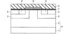
図8は、実施の形態1の炭化珪素半導体装置の一つのユニットセルを示す構成図である。実施の形態1ではSiC−MOSFET(Metal Oxide Semiconductor Field Effect Transistor)を炭化珪素半導体装置の例として説明する。実施の形態1のSiC−MOSFETは、n+型の半導体基板1と、半導体基板1上に形成されたn−型のSiC層2と、SiC層2の表面に選択的に形成されたウェル領域3と、ウェル領域3の表面に選択的に形成されたソース領域4及びコンタクト領域5を備えている。半導体基板1とSiC層2は、SiCウエハ6を構成している。さらに、実施の形態1のSiC−MOSFETは、ウェル領域3及びSiC層2上に亘って形成されたゲート酸化膜7と、ゲート酸化膜7上に形成されたゲート電極8と、ソース領域4上に形成されたソース電極10と、ゲート電極8を覆ってソース電極10との絶縁を確保する層間絶縁膜9と、ソース電極10及び層間絶縁膜9上に形成されたバリアメタル13と、バリアメタル13上に形成されたCu電極12とを備えている。
<A-1. Configuration>
FIG. 8 is a configuration diagram showing one unit cell of the silicon carbide semiconductor device of the first embodiment. In the first embodiment, a SiC-MOSFET (Metal Oxide Semiconductor Field Effect Transistor) will be described as an example of a silicon carbide semiconductor device. The SiC-MOSFET of the first embodiment includes an n +
<A−2.製造工程>
図8に示す構造のSiC−MOSFETの製造方法を図1〜7に沿って説明する。まずn+型の半導体基板1の一方面上に、エピタキシャル結晶成長法を用いて、SiCからなるn−型のSiC層2を形成する(図1)。半導体基板1としては、例えば、n+型のSiC基板が好適である。この半導体基板1とSiC層2がSiCウエハ6を構成する。
<A-2. Manufacturing process>
A method for manufacturing the SiC-MOSFET having the structure shown in FIG. 8 will be described with reference to FIGS. First, an n −
次にSiCウエハ6の表面内、具体的にはSiCウエハ6を構成するSiC層2の表面内の所定の間隔に離間した部位に、レジストをマスクとして不純物をイオン注入して、p型のウェル領域3を選択的に形成する(図2)。SiC層2内でp型となる不純物としては、例えばボロン(B)あるいはアルミニウム(Al)が挙げられる。イオン注入後、レジストは除去する。
Next, impurities are ion-implanted into the surface of the
次に、それぞれのウェル領域3の表面内に、レジストをマスクとして不純物をイオン注入して、n型のソース領域4を選択的に形成する(図2)。ウェル領域3内でn型となる不純物としては、例えばリン(P)あるいは窒素(N)が挙げられる。イオン注入後、レジストは除去する。
Next, impurities are ion-implanted into the surface of each
次に、ウェル領域3の表面内に、レジストをマスクとして、p型(第2導電型)の不純物をイオン注入して、ソース領域4の周囲に隣接して、p+型(第2導電型)のコンタクト領域5を形成する(図2)。ここではコンタクト領域5の不純物濃度は、ウェル領域3の不純物濃度より相対的に濃くなるように設定する。ウェル領域3内でp型となる不純物としては、例えばボロン(B)あるいはアルミニウム(Al)が挙げられる。イオン注入後、レジストは除去する。
Next, a p-type (second conductivity type) impurity is ion-implanted into the surface of the
次にSiCウエハ6に対し、アルゴン(Ar)などの不活性ガス雰囲気でアニール処理を行う。これにより、注入イオンが電気的に活性化され、かつイオン注入により形成された結晶欠陥が回復する。さらに、SiCウエハ6の一方面上、具体的にはイオン注入された側のSiCウエハ6上に、熱酸化法によって二酸化珪素(SiO2)からなるゲート酸化膜7を形成する(図3)。この工程で形成されるゲート酸化膜7は熱酸化膜である。
Next, the
次に、ゲート酸化膜7上に、化学気相成長法によりポリシリコン膜を形成した後、不要部分を、レジストをマスクとして、ウェットエッチング法あるいはRIEなどによるドライエッチング法により除去してゲート電極8を形成する(図4)。
Next, after a polysilicon film is formed on the
次に、ゲート酸化膜7及びゲート電極8の表面上に層間絶縁膜9を形成する(図5)。次に、レジストをマスクとして、ウェットエッチング法あるいはRIEなどによるドライエッチング法により、コンタクト領域5及び一部のソース領域4が露出するようにして、層間絶縁膜9及びゲート酸化膜7を除去する(図6)。その後、レジストを除去する。
Next, an
次に、層間絶縁膜9及びゲート酸化膜7が除去され露出したコンタクト領域5及びソース領域4上に、例えばスパッタリングなどの物理気相成長法により導電膜を形成する。その後、層間絶縁膜9の表面上に形成された導電膜の不要部分を、レジストをマスクとして、ウェットエッチング法あるいは反応性イオンエッチングなどによるドライエッチング法により除去して、コンタクト領域5及び一部のソース領域4上にソース電極10を形成する(図7)。次に半導体基板1の裏面にドレイン電極11を形成する。
Next, a conductive film is formed on the
次に、作製した素子構造にバリアメタル13とCu電極12を形成する(図8)。図1〜図8はMOSFETの最小基本素子構造であるユニットセルを示したが、図9〜図21では複数のユニットセルの集まりを素子構造部20とし、この素子構造部20上に形成するバリアメタル13やCu電極12の端部について詳細に説明する。なお、本明細書ではSiCウエハ6と素子構造部20からなる構成、すなわち図8に示したMOSFETからバリアメタル13とCu電極12を除いた構成を炭化珪素半導体素子とも呼ぶ。
Next, a
まず、素子構造部20の表面にCu拡散を防止するバリアメタル13を堆積する(図9)。バリアメタル13の材料には、W、Ta、Mo、Nb、Ir、Ru、Hf、Rh、V、Zr、Pt、Ti、Pd等の金属や、TiN、TiSiN、WN、WSiN、TaN、TaSiN、ZrN、AlN、BN、CrN、NbN等の窒化物、TaC、TiC、WC、NbC等の金属炭化物等を用いることができる。また、これらの任意の組み合わせの積層構造、例えばTi/TiN、Ti/TaN、Ta/TaN等も用いることができる。積層構造は3層以上でもよい。成膜は蒸着、スパッタ、CVD等を用いることができる。バリアメタル13の厚さは10〜500nmとする。
First, a
次に、このバリアメタル13上にCuめっき成膜の下地となるCu下地層12aを蒸着、スパッタ、CVD等で堆積する(図9)。Cu下地層12aの厚さは例えば100〜1000nmとする。そして、レジスト21を塗布、露光、現像することで、Cu下地層12a上のCuめっきを成膜させたくない部分にレジスト21をパターニングして形成しておく(図10)。レジスト21の厚さは、後に堆積するめっきCuの厚さよりも厚くしておくことが望ましい。レジスト21のエッジ部分の形状は、レジストボトム以外の一部の幅がレジストボトムより狭くなるようにする。この形状は、具体的には露光時のエネルギーや焦点を調整することにより実現する。図10ではレジストトップの幅が最も狭くなるようにレジスト21を形成しているが、レジストボトムよりレジストボトム以外の一部の幅が狭い形状である限り、図11に示すレジスト22のように、中部(レジストミドル)の幅が最も狭くなっていても良い。レジスト21,22において、最も幅の狭い部分とレジストボトムの幅の差分だけ、最終的なバリアメタル13表面に沿ったCu電極12とSiCウエハ6上に形成された素子構造部20との間の長さを長くすることができ、Cuがバリアメタル13界面を拡散して素子構造部20に到達してデバイス特性に影響を与える時間、すなわちCu拡散によるデバイス寿命をその分長くすることができる。ここではレジスト21,22における最も幅の狭い部分とレジストボトムの幅の差を、少なくともバリアメタル13の厚さの10倍以上とする。こうすることで、Cuが素子構造部20へ拡散することを防止するという効果について、実用上望ましいものが得られる。
Next, a
次に、Cuをめっき成膜してCuめっき層12bを形成する(図12)。Cuめっき層12bはレジスト21の無い部分に成膜されるので、レジスト21の側壁の形状をかたどった形状、つまり底部より上部のほうが幅が広い形状となる。Cuめっき層12bの厚さは例えば5〜100μmとする。図12では、レジスト21は上部が最も幅の狭い形状であるため、Cuめっき層12bは上部が最も幅の広い形状となった。しかし、図13のようにレジスト21の中部が最も幅の狭い形状である場合には、Cuめっき層12bは中部が最も幅の広い形状となる。いずれにせよ、Cuめっき層12bは底部よりも上部に、底部よりも幅の広い部分が存在すればよい。パワーデバイスの放熱性やアセンブリの観点から、Cuめっき層12bの厚さを5μm以上としている。Cu系電極を厚膜で形成することにより、熱容量を稼ぐことでチップ内の熱分布を均一化することが可能である。また、短絡時の温度の上昇を抑えることができ、耐量が向上する。ワイヤボンド時、径の大きいワイヤを打つので強い力がかかり、電極が薄いとデバイスにダメージが加わり、素子が破壊される。CuワイヤボンドはAlワイヤボンドよりも力がかかるため、Al系電極に比べて厚膜が必要とされる。このような場合において、Cuが素子構造部20へ拡散することを防止するためにこの発明は有用である。
Next, Cu is plated to form a
次に、レジスト21、Cu下地層12aを除去する(図14、図15)。レジスト21の除去には、有機溶剤や酸素プラズマ処理を、Cu下地層12aの除去には硫酸、塩酸、酢酸、燐酸、硝酸、フッ酸などの酸溶液やこれらの混合溶液、またこれらに過酸化水素を加えたものを用いることができる。
Next, the resist 21 and the
次に、Cuめっき層12bをマスクにして、バリアメタル13を垂直に異方性エッチングする(図16)。バリアメタル13としてTiNを用いて、RIE法によりエッチングする際の条件の一例を挙げると、プロセスガスとして、塩素(Cl2)ガスを用い、圧力を0.1Paとする。ここではTiNをエッチングする例を示したが、垂直に異方性エッチングを行う限りにおいて圧力、ガス種等は他の条件でも良い。また、TiN以外のバリアメタル13を用いる場合はそれに適したガス種を選択すればよい。異方性エッチングにRIEを用いた例を示したが、Arイオンミリング、スパッタエッチ等も用いることができる。
Next, the
こうして、Cu下地層12aとCuめっき層12bからなるCu電極12が形成された。バリアメタル13は、Cu電極12のバリアメタル13と接する幅よりも幅広に形成されている。これにより、バリアメタル13表面に沿ったCu電極12とSiCウエハ6上に形成された素子構造部20との間の長さを長くすることができ、高いCu拡散防止効果を得ることができる。また、バリアメタル13のエッジで発生する大きな応力がCu膜剥がれの起点となるCu膜エッジにかかることを抑制できるため、Cu膜剥がれを抑制できる。これは特に、膜剥がれが発生しやすい5μmを超えるような厚いCu電極を用いた場合に有効である。これにより、信頼性の高い電力半導体を実現することができる。
Thus, the
なお、本実施の形態では電力半導体素子の一例としてSiC−MOSFETを挙げて説明したが、SBDやJFET、IGBT、PNダイオードでも本発明を適用して信頼性の高いCu電極を形成することができる。 In this embodiment, the SiC-MOSFET is described as an example of the power semiconductor element. However, the present invention can be applied to an SBD, JFET, IGBT, or PN diode to form a highly reliable Cu electrode. .
<A−3.効果>
本実施の形態の炭化珪素半導体装置は、炭化珪素半導体素子(SiCウエハ6、素子構造部20)と、素子構造部20上に形成されたバリアメタル13と、バリアメタル13上に形成され、バリアメタル13との接触面の端部がバリアメタル13の端部よりも後退したCu電極12とを備える。また、Cu電極12は、バリアメタル13と接触する底部以外の少なくとも一部の幅が底部の幅よりも広い形状である。Cu電極12がバリアメタル13上に選択的に形成されることにより、バリアメタル13の表面に沿ったCu電極12と素子構造部20との距離が、バリアメタル13の端部とCu電極12の端部の位置ずれ量だけ長くなるため、バリアメタル13の表面に沿ったCuの素子構造部20への拡散を抑制する。また、バリアメタル13の端部の応力がCu電極12端部に加わることを防ぎ、Cu電極12の膜剥がれを抑制する。
<A-3. Effect>
The silicon carbide semiconductor device of the present embodiment includes a silicon carbide semiconductor element (
上記の構成によれば、Cu電極12の厚さは5μm以上と厚膜にしても、Cu電極12の膜剥がれを抑制することが可能である。
According to said structure, even if the thickness of
また、バリアメタル13の端部からバリアメタル13に接触したCu電極12の端部までの距離を、バリアメタル13の厚みの10倍以上とすることにより、Cuの炭化珪素半導体素子への拡散を抑制する効果が特に発揮される。
Further, by making the distance from the end of the
本実施の形態の炭化珪素半導体装置の製造方法は、(a)炭化珪素半導体素子(SiCウエハ6、素子構造部20)上にバリアメタル13を形成する工程と、(b)バリアメタル13上に、バリアメタル13との接触面の端部がバリアメタル13の端部よりも後退したCu電極12を形成する工程と、(c)Cu電極12をマスクにしてバリアメタル13を垂直に異方性エッチングする工程とを備え、工程(b)は、Cu電極12をバリアメタル13と接触する底部以外の少なくとも一部の幅が底部の幅よりも広くなるように形成する工程である。Cu電極12がバリアメタル13と接する幅よりも幅広にバリアメタル13が形成される。そのため、バリアメタル13表面に沿ったCuと素子構造部20との距離を長くすることができ、高いCu拡散防止効果が得られる。また、バリアメタル13の端部で発生する応力がCu電極12の端部に加わることを防ぐので、Cu電極12の膜剥がれが抑制される。
The method for manufacturing a silicon carbide semiconductor device of the present embodiment includes (a) a step of forming a
また、工程(b)は、Cu電極12を厚み5μm以上で形成する工程である。Cu電極12を5μm以上と厚膜に形成すると、膜応力が大きくなりCu電極12の膜剥がれが懸念されるところ、Cu電極12端部とバリアメタル13端部の位置が異なるため、バリアメタル13の端部の応力がCu電極12端部に加わることが防がれ、膜剥がれを抑制できる。
Step (b) is a step of forming the
また、工程(b)は、(b1)バリアメタル上にCu下地層をスパッタ、蒸着、CVDのいずれかで堆積する工程と、(b2)Cu下地層上にレジストを用いて選択的に電界めっきでCuめっき層を形成する工程と、(b3)Cuめっき層が形成されない部分のCu下地層を、硫酸、塩酸、酢酸、燐酸、硝酸、フッ酸、またはこれらの混合溶液、またこれらに過酸化水素を加えた溶液で除去する工程とを備える。以上の工程により、所望の形状のCu電極12を形成することが可能である。
Step (b) includes (b1) a step of depositing a Cu underlayer on the barrier metal by sputtering, vapor deposition, or CVD, and (b2) selective electroplating using a resist on the Cu underlayer. A step of forming a Cu plating layer with (b3) a portion of the Cu underlayer on which the Cu plating layer is not formed, sulfuric acid, hydrochloric acid, acetic acid, phosphoric acid, nitric acid, hydrofluoric acid, or a mixed solution thereof, or a peroxide thereof Removing with a solution to which hydrogen has been added. Through the above steps, it is possible to form a
また、工程(b2)は、底部以外の少なくとも一部の幅が底部の幅よりも狭いレジスト21,22を用いて、Cuめっき層12bを形成する工程である。これにより、Cuめっき層12bの底部以外の少なくとも一部の幅が底部の幅よりも広く形成されるので、Cuめっき層12bを用いた垂直方向のエッチングにより、バリアメタル13の幅がCu電極12と接触する幅よりも広い構造が形成できる。
The step (b2) is a step of forming the
<B.実施の形態2>
<B−1.製造工程>
実施の形態1ではレジストボトムよりレジストボトム以外の一部の幅が狭い形状のレジストを用いてCu成膜することでCuボトムよりCu上部の方が幅が広い形状になるようにし、バリアメタルをこのCu膜をマスクにして垂直に異方性エッチングすることでバリアメタル表面に沿ったCuと基板上に形成された素子構造部との間の長さを長くした炭化珪素半導体装置とその製造方法を説明した。実施の形態1における炭化珪素半導体装置はCu拡散防止効果を得ることができ、Cu膜剥がれを防止できる。実施の形態2では同様に高いCu拡散防止効果を得ることができ、Cu膜剥がれを防止できる炭化珪素半導体装置とその製造方法を説明する。なお、Cu、バリアメタル形成工程以外の工程については実施の形態1において図1〜8を用いて説明したものと同じであるため、ここでは説明を省略する。
<B. Second Embodiment>
<B-1. Manufacturing process>
In the first embodiment, Cu film formation is performed using a resist having a shape that is narrower than the resist bottom, and the width of the upper part of the Cu is wider than that of the Cu bottom. Silicon carbide semiconductor device in which the length between Cu along the barrier metal surface and the element structure formed on the substrate is increased by anisotropic etching perpendicularly using this Cu film as a mask, and a method for manufacturing the same Explained. The silicon carbide semiconductor device in the first embodiment can obtain an effect of preventing Cu diffusion and can prevent peeling of the Cu film. In the second embodiment, a silicon carbide semiconductor device capable of obtaining a high Cu diffusion preventing effect and preventing Cu film peeling and a manufacturing method thereof will be described. Since steps other than the Cu and barrier metal forming step are the same as those described in the first embodiment with reference to FIGS. 1 to 8, description thereof is omitted here.
まず、実施の形態1と同様に基板表面にCu拡散を防止するバリアメタルを堆積する(図9)。バリアメタルとしてはW、Ta、Mo、Nb、Ir、Ru、Hf、Rh、V、Zr、Pt、Ti、Pd等の金属や、TiN、TiSiN、WN、WSiN、TaN、TaSiN、ZrN、AlN、BN、CrN、NbN等の窒化物、TaC、TiC、WC、NbC等の金属炭化物等を用いることができる。また、これらの任意の組み合わせの積層構造、例えばTi/TiN、Ti/TaN、Ta/TaN等も用いることができる。積層構造は3層以上でもよい。成膜は蒸着、スパッタ、CVD等を用いることができる。バリアメタルの厚さは10〜500nmとする。このバリアメタル上にCuめっき成膜の下地となるCuを蒸着、スパッタ、CVD等で堆積する(図9)。厚さは例えば100〜1000nmとする。 First, a barrier metal for preventing Cu diffusion is deposited on the substrate surface as in the first embodiment (FIG. 9). As barrier metals, metals such as W, Ta, Mo, Nb, Ir, Ru, Hf, Rh, V, Zr, Pt, Ti, Pd, TiN, TiSiN, WN, WSiN, TaN, TaSiN, ZrN, AlN, A nitride such as BN, CrN, or NbN, or a metal carbide such as TaC, TiC, WC, or NbC can be used. A laminated structure of any combination of these, for example, Ti / TiN, Ti / TaN, Ta / TaN, etc. can also be used. The laminated structure may be three or more layers. Vapor deposition, sputtering, CVD, etc. can be used for film formation. The thickness of the barrier metal is 10 to 500 nm. On this barrier metal, Cu as a base for Cu plating film formation is deposited by vapor deposition, sputtering, CVD or the like (FIG. 9). The thickness is, for example, 100 to 1000 nm.
次に、レジスト22を塗布、露光、現像することで、Cu下地層12a上のCuめっき層12bを成膜させたくない部分にレジスト23をパターンニングして形成しておく(図17)。レジスト22の厚さは後に堆積するCuめっき層12bの厚さよりも薄くする点が、実施の形態1とは異なる。このレジスト22をマスクに用いてCuめっき層12bを成膜することにより、図18に示すようにCuめっき層12bはレジスト22を越えて形成される結果、レジスト22を越えた部分ではCuめっき層12bが横方向にも成長し、幅の広い形状となる。
Next, by applying, exposing and developing a resist 22, a resist 23 is patterned and formed on a portion where the
次に、レジスト22、Cu12aを除去する(図19、図20)。レジスト22の除去には有機溶剤や酸素プラズマ処理を、Cu12aの除去には硫酸、塩酸、酢酸、燐酸、硝酸、フッ酸などの酸溶液やこれらの混合溶液、またこれらに過酸化水素を加えたものを用いることができる。 Next, the resist 22 and Cu12a are removed (FIGS. 19 and 20). An organic solvent or oxygen plasma treatment was used to remove the resist 22, and an acid solution such as sulfuric acid, hydrochloric acid, acetic acid, phosphoric acid, nitric acid or hydrofluoric acid or a mixed solution thereof was added to the Cu12a, or hydrogen peroxide was added thereto. Things can be used.
次に、バリアメタル13をCuめっき層12bをマスクにして垂直に異方性エッチングする(図21)。ここではバリアメタルとしてTiNを用いて、RIE法によりエッチングする際の条件の一例を挙げると、プロセスガスとして、塩素(Cl2)ガスを用い、圧力を0.1Paとする。ここではTiNをエッチングする例を示したが、圧力、ガス種等は垂直に異方性エッチングができればよく、この条件に限られるものではない。また、TiN以外のバリアメタル13を用いる場合はそれに適したガス種を選択すればよい。異方性エッチングにRIEを用いた例を示したが、Arイオンミリング、スパッタエッチ等も用いることができる。
Next, the
この実施の形態により、Cu電極のバリアメタル13と接する幅よりも幅の広いバリアメタル13をもったバリアメタル/Cu配線構造を得ることができる。バリアメタル13の幅は、Cuめっき層12bのうちレジスト22を越えて成膜された上部の幅と同じになる。このCuめっき層12bの上部の幅とレジスト22開口幅の差分だけ、最終的なバリアメタル13界面に沿ったCu電極12とSiCウエハ6上に形成された素子構造部20との間の長さを長くすることができ、Cuがバリアメタル13界面を拡散して素子構造部20に到達してデバイス特性に影響を与える時間、すなわちCu拡散によるデバイス寿命をその分長くすることができる。レジスト22を越えてCuめっき層12bを成膜した際、Cuめっき層12bの横方向の成長速度は縦方向の成長速度に等しいため、Cuめっき層12bの上部の幅とレジスト開口幅の差分は、Cuめっき層12bの厚さとレジスト22の厚さの差分に等しくなる。ここではレジスト22の厚さとCuめっき層12bの厚さの差を、少なくともバリアメタル13の厚さの10倍以上とする。
According to this embodiment, it is possible to obtain a barrier metal / Cu wiring structure having a
これにより、バリアメタル13界面に沿ったCu電極12とSiCウエハ6上に形成された素子構造部20との間の長さを長くすることができ、高いCu拡散防止効果を得ることができる。また、バリアメタル13のエッジで発生する大きな応力がCu膜剥がれの起点となるCu電極12のエッジにかかることを抑制できるため、Cu膜剥がれを抑制できる。
Thereby, the length between the
<B−2.効果>
実施の形態2に記載の炭化珪素半導体装置の製造方法では、Cu下地層12a上にレジスト23を用いて選択的に電界めっきでレジスト23の厚さよりも厚いCuめっき層12bを形成する.よってCuめっき層12bは、レジスト23の厚みを超えた部分の幅が底部の幅よりも広く形成されるので、Cuめっき層12bを用いた垂直方向のエッチングにより、バリアメタルの幅がCu電極12と接触する幅よりも広い構造を形成できる。
<B-2. Effect>
In the method for manufacturing the silicon carbide semiconductor device described in the second embodiment,
なお、本発明は、その発明の範囲内において、各実施の形態を自由に組み合わせたり、各実施の形態を適宜、変形、省略することが可能である。 It should be noted that the present invention can be freely combined with each other within the scope of the invention, and each embodiment can be appropriately modified or omitted.
1 半導体基板、2 SiC層、3 ウェル領域、4 ソース領域、5 コンタクト領域、6 SiCウエハ、7 ゲート酸化膜、8 ゲート電極、9 層間絶縁膜、10 ソース電極、11 ドレイン電極、12 Cu電極、12a Cu下地層、12b Cuめっき層、13 バリアメタル、20 素子構造部、21〜23 レジスト。 1 semiconductor substrate, 2 SiC layer, 3 well region, 4 source region, 5 contact region, 6 SiC wafer, 7 gate oxide film, 8 gate electrode, 9 interlayer insulation film, 10 source electrode, 11 drain electrode, 12 Cu electrode, 12a Cu underlayer, 12b Cu plating layer, 13 barrier metal, 20 element structure, 21-23 resist.
Claims (7)
前記炭化珪素半導体素子上に形成されたバリアメタルと、
前記バリアメタル上に形成され、前記バリアメタルとの接触面の端部が前記バリアメタルの端部よりも後退した、厚さが5μm以上であるCu電極とを備える、
炭化珪素半導体装置。 A silicon carbide semiconductor element;
A barrier metal formed on the silicon carbide semiconductor element;
A Cu electrode formed on the barrier metal and having a thickness of 5 μm or more, wherein an end portion of a contact surface with the barrier metal recedes from an end portion of the barrier metal;
Silicon carbide semiconductor device.
請求項1に記載の炭化珪素半導体装置。 The Cu electrode has a shape in which the width of at least a portion other than the bottom contacting the barrier metal is wider than the width of the bottom.
The silicon carbide semiconductor device according to claim 1.
請求項1又は2に記載の炭化珪素半導体装置。The silicon carbide semiconductor device according to claim 1 or 2.
(b)前記バリアメタル上に、前記バリアメタルとの接触面の端部が前記バリアメタルの端部よりも後退した、厚さが5μm以上であるCu電極を形成する工程と、 (B) forming, on the barrier metal, a Cu electrode having a thickness of 5 μm or more, wherein an end of a contact surface with the barrier metal is recessed from an end of the barrier metal;
(c)前記Cu電極をマスクにして前記バリアメタルを垂直に異方性エッチングする工程とを備え、 (C) a step of anisotropically etching the barrier metal vertically using the Cu electrode as a mask,
前記工程(b)は、前記Cu電極を、前記バリアメタルと接触する底部以外の少なくとも一部の幅が前記底部の幅よりも広くなるように形成する工程である、 The step (b) is a step of forming the Cu electrode such that at least a part of the width other than the bottom contacting the barrier metal is wider than the width of the bottom.
炭化珪素半導体装置の製造方法。A method for manufacturing a silicon carbide semiconductor device.
(b1)前記バリアメタル上にCu下地層をスパッタ、蒸着、CVDのいずれかで堆積する工程と、 (B1) a step of depositing a Cu underlayer on the barrier metal by any one of sputtering, vapor deposition, and CVD;
(b2)前記Cu下地層上にレジストを用いて選択的に電界めっきでCuめっき層を形成する工程と、 (B2) a step of selectively forming a Cu plating layer by electroplating using a resist on the Cu underlayer;
(b3)前記Cuめっき層が形成されない部分の前記Cu下地層を、硫酸、塩酸、酢酸、燐酸、硝酸、フッ酸、またはこれらの混合溶液、またこれらに過酸化水素を加えた溶液で除去する工程とを備える、 (B3) The Cu underlayer where the Cu plating layer is not formed is removed with sulfuric acid, hydrochloric acid, acetic acid, phosphoric acid, nitric acid, hydrofluoric acid, or a mixed solution thereof, or a solution obtained by adding hydrogen peroxide to these. A process,
請求項4に記載の炭化珪素半導体装置の製造方法。A method for manufacturing a silicon carbide semiconductor device according to claim 4.
請求項5に記載の炭化珪素半導体装置の製造方法。A method for manufacturing a silicon carbide semiconductor device according to claim 5.
請求項5に記載の炭化珪素半導体装置の製造方法。A method for manufacturing a silicon carbide semiconductor device according to claim 5.
Priority Applications (1)
| Application Number | Priority Date | Filing Date | Title |
|---|---|---|---|
| JP2012264901A JP5889171B2 (en) | 2012-12-04 | 2012-12-04 | Silicon carbide semiconductor device and manufacturing method thereof |
Applications Claiming Priority (1)
| Application Number | Priority Date | Filing Date | Title |
|---|---|---|---|
| JP2012264901A JP5889171B2 (en) | 2012-12-04 | 2012-12-04 | Silicon carbide semiconductor device and manufacturing method thereof |
Publications (2)
| Publication Number | Publication Date |
|---|---|
| JP2014110362A JP2014110362A (en) | 2014-06-12 |
| JP5889171B2 true JP5889171B2 (en) | 2016-03-22 |
Family
ID=51030822
Family Applications (1)
| Application Number | Title | Priority Date | Filing Date |
|---|---|---|---|
| JP2012264901A Active JP5889171B2 (en) | 2012-12-04 | 2012-12-04 | Silicon carbide semiconductor device and manufacturing method thereof |
Country Status (1)
| Country | Link |
|---|---|
| JP (1) | JP5889171B2 (en) |
Families Citing this family (10)
| Publication number | Priority date | Publication date | Assignee | Title |
|---|---|---|---|---|
| JP6378936B2 (en) | 2014-05-28 | 2018-08-22 | 株式会社ミツトヨ | Optical device |
| JP6347442B2 (en) * | 2014-08-19 | 2018-06-27 | 国立研究開発法人産業技術総合研究所 | Method for manufacturing silicon carbide semiconductor device |
| DE112015006381T5 (en) | 2015-03-27 | 2017-12-14 | Mitsubishi Electric Corporation | SEMICONDUCTOR UNIT AND METHOD FOR THE PRODUCTION THEREOF |
| JP6473512B2 (en) * | 2015-09-11 | 2019-02-20 | 株式会社日立製作所 | Semiconductor device and method for manufacturing the same, power module, power conversion device, and railcar |
| JP6690985B2 (en) * | 2016-02-24 | 2020-04-28 | 株式会社神戸製鋼所 | Ohmic electrode |
| WO2017145694A1 (en) * | 2016-02-24 | 2017-08-31 | 株式会社神戸製鋼所 | Ohmic electrode |
| DE102016104788B4 (en) | 2016-03-15 | 2019-06-19 | Infineon Technologies Ag | A semiconductor device having a metal adhesion and barrier structure and method of manufacturing a semiconductor device |
| WO2017169086A1 (en) * | 2016-03-30 | 2017-10-05 | 三菱電機株式会社 | Semiconductor device, method for manufacturing same, and power conversion device |
| JP2022167237A (en) * | 2021-04-22 | 2022-11-04 | 有限会社Mtec | Semiconductor device manufacturing method and vertical MOSFET device |
| JP7644658B2 (en) | 2021-05-26 | 2025-03-12 | 東京応化工業株式会社 | Chemicals used in etching processes |
Family Cites Families (4)
| Publication number | Priority date | Publication date | Assignee | Title |
|---|---|---|---|---|
| JPS58135638A (en) * | 1982-02-05 | 1983-08-12 | Mitsubishi Electric Corp | Manufacture of semiconductor device |
| JPH06151355A (en) * | 1992-10-30 | 1994-05-31 | Mitsubishi Electric Corp | Semiconductor device and manufacture thereof |
| US8093598B2 (en) * | 2006-03-22 | 2012-01-10 | Mitsubishi Electric Corporation | Power semiconductor device |
| JP2010056136A (en) * | 2008-08-26 | 2010-03-11 | Toshiba Mobile Display Co Ltd | Wiring, method of manufacturing the same, thin film transistor, and display element |
-
2012
- 2012-12-04 JP JP2012264901A patent/JP5889171B2/en active Active
Also Published As
| Publication number | Publication date |
|---|---|
| JP2014110362A (en) | 2014-06-12 |
Similar Documents
| Publication | Publication Date | Title |
|---|---|---|
| JP5889171B2 (en) | Silicon carbide semiconductor device and manufacturing method thereof | |
| JP5728339B2 (en) | Semiconductor device and manufacturing method of semiconductor device | |
| JP4858791B2 (en) | Semiconductor device and manufacturing method thereof | |
| JP5525940B2 (en) | Semiconductor device and manufacturing method of semiconductor device | |
| US8093598B2 (en) | Power semiconductor device | |
| US8766334B2 (en) | Semiconductor device with low resistance gate electrode and method of manufacturing the same | |
| JP5955246B2 (en) | Manufacturing method of semiconductor device | |
| JP5792701B2 (en) | Semiconductor device and manufacturing method thereof | |
| JP5860580B2 (en) | Semiconductor device and manufacturing method thereof | |
| TW200845206A (en) | Method for manufacturing insulated gate field effect transistor | |
| WO2016080269A1 (en) | Semiconductor device and method for producing semiconductor device | |
| JPWO2010125661A1 (en) | Semiconductor device and manufacturing method thereof | |
| JP2013055214A (en) | Semiconductor device and manufacturing method therefor | |
| JP7605241B2 (en) | Method for manufacturing a trench type semiconductor device | |
| JP2012160485A (en) | Semiconductor device and manufacturing method of the same | |
| JP2010086999A (en) | Back electrode for semiconductor device, semiconductor device, and manufacturing method of back electrode for semiconductor device | |
| US10032894B2 (en) | Silicon carbide semiconductor device and method of manufacturing silicon carbide semiconductor device | |
| WO2015001863A1 (en) | Method for manufacturing silicon carbide semiconductor device | |
| JP4091931B2 (en) | SiC semiconductor device and method of manufacturing SiC semiconductor device | |
| CN107195616B (en) | Semiconductor device including metal adhesion and barrier structures and method of forming the same | |
| JP2011129750A (en) | Method of manufacturing high breakdown voltage semiconductor element and structure thereof | |
| JP2017168679A (en) | Silicon carbide semiconductor element and silicon carbide semiconductor element manufacturing method | |
| JP2011233643A (en) | Semiconductor device and manufacturing method thereof |
Legal Events
| Date | Code | Title | Description |
|---|---|---|---|
| A621 | Written request for application examination |
Free format text: JAPANESE INTERMEDIATE CODE: A621 Effective date: 20141003 |
|
| A977 | Report on retrieval |
Free format text: JAPANESE INTERMEDIATE CODE: A971007 Effective date: 20150612 |
|
| A131 | Notification of reasons for refusal |
Free format text: JAPANESE INTERMEDIATE CODE: A131 Effective date: 20150623 |
|
| A521 | Request for written amendment filed |
Free format text: JAPANESE INTERMEDIATE CODE: A523 Effective date: 20150819 |
|
| TRDD | Decision of grant or rejection written | ||
| A01 | Written decision to grant a patent or to grant a registration (utility model) |
Free format text: JAPANESE INTERMEDIATE CODE: A01 Effective date: 20160119 |
|
| A61 | First payment of annual fees (during grant procedure) |
Free format text: JAPANESE INTERMEDIATE CODE: A61 Effective date: 20160216 |
|
| R150 | Certificate of patent or registration of utility model |
Ref document number: 5889171 Country of ref document: JP Free format text: JAPANESE INTERMEDIATE CODE: R150 |
|
| R250 | Receipt of annual fees |
Free format text: JAPANESE INTERMEDIATE CODE: R250 |
|
| R250 | Receipt of annual fees |
Free format text: JAPANESE INTERMEDIATE CODE: R250 |
|
| R250 | Receipt of annual fees |
Free format text: JAPANESE INTERMEDIATE CODE: R250 |
|
| R250 | Receipt of annual fees |
Free format text: JAPANESE INTERMEDIATE CODE: R250 |
|
| R250 | Receipt of annual fees |
Free format text: JAPANESE INTERMEDIATE CODE: R250 |
|
| R250 | Receipt of annual fees |
Free format text: JAPANESE INTERMEDIATE CODE: R250 |
|
| R250 | Receipt of annual fees |
Free format text: JAPANESE INTERMEDIATE CODE: R250 |