JP5867877B2 - Electronic textile and method for producing electronic textile - Google Patents
Electronic textile and method for producing electronic textile Download PDFInfo
- Publication number
- JP5867877B2 JP5867877B2 JP2013528799A JP2013528799A JP5867877B2 JP 5867877 B2 JP5867877 B2 JP 5867877B2 JP 2013528799 A JP2013528799 A JP 2013528799A JP 2013528799 A JP2013528799 A JP 2013528799A JP 5867877 B2 JP5867877 B2 JP 5867877B2
- Authority
- JP
- Japan
- Prior art keywords
- textile
- textile carrier
- component
- electronic
- support plate
- Prior art date
- Legal status (The legal status is an assumption and is not a legal conclusion. Google has not performed a legal analysis and makes no representation as to the accuracy of the status listed.)
- Expired - Fee Related
Links
- 239000004753 textile Substances 0.000 title claims description 131
- 238000004519 manufacturing process Methods 0.000 title claims description 16
- 239000004020 conductor Substances 0.000 claims description 73
- 238000000034 method Methods 0.000 claims description 26
- 239000000853 adhesive Substances 0.000 claims description 10
- 230000001070 adhesive effect Effects 0.000 claims description 10
- 239000003550 marker Substances 0.000 claims description 6
- 239000012790 adhesive layer Substances 0.000 claims description 2
- 239000000969 carrier Substances 0.000 claims description 2
- 238000003825 pressing Methods 0.000 claims description 2
- 239000000758 substrate Substances 0.000 description 6
- 239000000835 fiber Substances 0.000 description 4
- 238000010586 diagram Methods 0.000 description 2
- 238000009940 knitting Methods 0.000 description 2
- 229910000679 solder Inorganic materials 0.000 description 2
- 230000037303 wrinkles Effects 0.000 description 2
- 230000001419 dependent effect Effects 0.000 description 1
- 238000005516 engineering process Methods 0.000 description 1
- 239000003822 epoxy resin Substances 0.000 description 1
- 239000004744 fabric Substances 0.000 description 1
- 238000009950 felting Methods 0.000 description 1
- 239000000463 material Substances 0.000 description 1
- 230000035515 penetration Effects 0.000 description 1
- 229920000647 polyepoxide Polymers 0.000 description 1
- 238000007650 screen-printing Methods 0.000 description 1
- 238000009941 weaving Methods 0.000 description 1
Images


Classifications
-
- H—ELECTRICITY
- H05—ELECTRIC TECHNIQUES NOT OTHERWISE PROVIDED FOR
- H05K—PRINTED CIRCUITS; CASINGS OR CONSTRUCTIONAL DETAILS OF ELECTRIC APPARATUS; MANUFACTURE OF ASSEMBLAGES OF ELECTRICAL COMPONENTS
- H05K1/00—Printed circuits
- H05K1/02—Details
- H05K1/0277—Bendability or stretchability details
- H05K1/0283—Stretchable printed circuits
-
- F—MECHANICAL ENGINEERING; LIGHTING; HEATING; WEAPONS; BLASTING
- F21—LIGHTING
- F21K—NON-ELECTRIC LIGHT SOURCES USING LUMINESCENCE; LIGHT SOURCES USING ELECTROCHEMILUMINESCENCE; LIGHT SOURCES USING CHARGES OF COMBUSTIBLE MATERIAL; LIGHT SOURCES USING SEMICONDUCTOR DEVICES AS LIGHT-GENERATING ELEMENTS; LIGHT SOURCES NOT OTHERWISE PROVIDED FOR
- F21K9/00—Light sources using semiconductor devices as light-generating elements, e.g. using light-emitting diodes [LED] or lasers
- F21K9/20—Light sources comprising attachment means
-
- F—MECHANICAL ENGINEERING; LIGHTING; HEATING; WEAPONS; BLASTING
- F21—LIGHTING
- F21V—FUNCTIONAL FEATURES OR DETAILS OF LIGHTING DEVICES OR SYSTEMS THEREOF; STRUCTURAL COMBINATIONS OF LIGHTING DEVICES WITH OTHER ARTICLES, NOT OTHERWISE PROVIDED FOR
- F21V21/00—Supporting, suspending, or attaching arrangements for lighting devices; Hand grips
-
- H—ELECTRICITY
- H05—ELECTRIC TECHNIQUES NOT OTHERWISE PROVIDED FOR
- H05K—PRINTED CIRCUITS; CASINGS OR CONSTRUCTIONAL DETAILS OF ELECTRIC APPARATUS; MANUFACTURE OF ASSEMBLAGES OF ELECTRICAL COMPONENTS
- H05K1/00—Printed circuits
- H05K1/02—Details
- H05K1/0277—Bendability or stretchability details
-
- H—ELECTRICITY
- H05—ELECTRIC TECHNIQUES NOT OTHERWISE PROVIDED FOR
- H05K—PRINTED CIRCUITS; CASINGS OR CONSTRUCTIONAL DETAILS OF ELECTRIC APPARATUS; MANUFACTURE OF ASSEMBLAGES OF ELECTRICAL COMPONENTS
- H05K1/00—Printed circuits
- H05K1/02—Details
- H05K1/03—Use of materials for the substrate
- H05K1/038—Textiles
-
- H—ELECTRICITY
- H05—ELECTRIC TECHNIQUES NOT OTHERWISE PROVIDED FOR
- H05K—PRINTED CIRCUITS; CASINGS OR CONSTRUCTIONAL DETAILS OF ELECTRIC APPARATUS; MANUFACTURE OF ASSEMBLAGES OF ELECTRICAL COMPONENTS
- H05K1/00—Printed circuits
- H05K1/02—Details
- H05K1/11—Printed elements for providing electric connections to or between printed circuits
- H05K1/111—Pads for surface mounting, e.g. lay-out
-
- H—ELECTRICITY
- H05—ELECTRIC TECHNIQUES NOT OTHERWISE PROVIDED FOR
- H05K—PRINTED CIRCUITS; CASINGS OR CONSTRUCTIONAL DETAILS OF ELECTRIC APPARATUS; MANUFACTURE OF ASSEMBLAGES OF ELECTRICAL COMPONENTS
- H05K1/00—Printed circuits
- H05K1/18—Printed circuits structurally associated with non-printed electric components
- H05K1/181—Printed circuits structurally associated with non-printed electric components associated with surface mounted components
-
- H—ELECTRICITY
- H05—ELECTRIC TECHNIQUES NOT OTHERWISE PROVIDED FOR
- H05K—PRINTED CIRCUITS; CASINGS OR CONSTRUCTIONAL DETAILS OF ELECTRIC APPARATUS; MANUFACTURE OF ASSEMBLAGES OF ELECTRICAL COMPONENTS
- H05K1/00—Printed circuits
- H05K1/18—Printed circuits structurally associated with non-printed electric components
- H05K1/189—Printed circuits structurally associated with non-printed electric components characterised by the use of a flexible or folded printed circuit
-
- H—ELECTRICITY
- H05—ELECTRIC TECHNIQUES NOT OTHERWISE PROVIDED FOR
- H05K—PRINTED CIRCUITS; CASINGS OR CONSTRUCTIONAL DETAILS OF ELECTRIC APPARATUS; MANUFACTURE OF ASSEMBLAGES OF ELECTRICAL COMPONENTS
- H05K3/00—Apparatus or processes for manufacturing printed circuits
- H05K3/30—Assembling printed circuits with electric components, e.g. with resistor
- H05K3/303—Surface mounted components, e.g. affixing before soldering, aligning means, spacing means
-
- H—ELECTRICITY
- H05—ELECTRIC TECHNIQUES NOT OTHERWISE PROVIDED FOR
- H05K—PRINTED CIRCUITS; CASINGS OR CONSTRUCTIONAL DETAILS OF ELECTRIC APPARATUS; MANUFACTURE OF ASSEMBLAGES OF ELECTRICAL COMPONENTS
- H05K3/00—Apparatus or processes for manufacturing printed circuits
- H05K3/30—Assembling printed circuits with electric components, e.g. with resistor
- H05K3/32—Assembling printed circuits with electric components, e.g. with resistor electrically connecting electric components or wires to printed circuits
- H05K3/321—Assembling printed circuits with electric components, e.g. with resistor electrically connecting electric components or wires to printed circuits by conductive adhesives
-
- H—ELECTRICITY
- H05—ELECTRIC TECHNIQUES NOT OTHERWISE PROVIDED FOR
- H05K—PRINTED CIRCUITS; CASINGS OR CONSTRUCTIONAL DETAILS OF ELECTRIC APPARATUS; MANUFACTURE OF ASSEMBLAGES OF ELECTRICAL COMPONENTS
- H05K2201/00—Indexing scheme relating to printed circuits covered by H05K1/00
- H05K2201/02—Fillers; Particles; Fibers; Reinforcement materials
- H05K2201/0275—Fibers and reinforcement materials
- H05K2201/0281—Conductive fibers
-
- H—ELECTRICITY
- H05—ELECTRIC TECHNIQUES NOT OTHERWISE PROVIDED FOR
- H05K—PRINTED CIRCUITS; CASINGS OR CONSTRUCTIONAL DETAILS OF ELECTRIC APPARATUS; MANUFACTURE OF ASSEMBLAGES OF ELECTRICAL COMPONENTS
- H05K2201/00—Indexing scheme relating to printed circuits covered by H05K1/00
- H05K2201/02—Fillers; Particles; Fibers; Reinforcement materials
- H05K2201/0275—Fibers and reinforcement materials
- H05K2201/029—Woven fibrous reinforcement or textile
-
- H—ELECTRICITY
- H05—ELECTRIC TECHNIQUES NOT OTHERWISE PROVIDED FOR
- H05K—PRINTED CIRCUITS; CASINGS OR CONSTRUCTIONAL DETAILS OF ELECTRIC APPARATUS; MANUFACTURE OF ASSEMBLAGES OF ELECTRICAL COMPONENTS
- H05K2201/00—Indexing scheme relating to printed circuits covered by H05K1/00
- H05K2201/10—Details of components or other objects attached to or integrated in a printed circuit board
- H05K2201/10007—Types of components
- H05K2201/10106—Light emitting diode [LED]
-
- H—ELECTRICITY
- H05—ELECTRIC TECHNIQUES NOT OTHERWISE PROVIDED FOR
- H05K—PRINTED CIRCUITS; CASINGS OR CONSTRUCTIONAL DETAILS OF ELECTRIC APPARATUS; MANUFACTURE OF ASSEMBLAGES OF ELECTRICAL COMPONENTS
- H05K2203/00—Indexing scheme relating to apparatus or processes for manufacturing printed circuits covered by H05K3/00
- H05K2203/01—Tools for processing; Objects used during processing
- H05K2203/0147—Carriers and holders
- H05K2203/0152—Temporary metallic carrier, e.g. for transferring material
-
- Y—GENERAL TAGGING OF NEW TECHNOLOGICAL DEVELOPMENTS; GENERAL TAGGING OF CROSS-SECTIONAL TECHNOLOGIES SPANNING OVER SEVERAL SECTIONS OF THE IPC; TECHNICAL SUBJECTS COVERED BY FORMER USPC CROSS-REFERENCE ART COLLECTIONS [XRACs] AND DIGESTS
- Y10—TECHNICAL SUBJECTS COVERED BY FORMER USPC
- Y10T—TECHNICAL SUBJECTS COVERED BY FORMER US CLASSIFICATION
- Y10T29/00—Metal working
- Y10T29/49—Method of mechanical manufacture
- Y10T29/49002—Electrical device making
- Y10T29/49117—Conductor or circuit manufacturing
- Y10T29/49124—On flat or curved insulated base, e.g., printed circuit, etc.
- Y10T29/4913—Assembling to base an electrical component, e.g., capacitor, etc.
Landscapes
- Engineering & Computer Science (AREA)
- Microelectronics & Electronic Packaging (AREA)
- Manufacturing & Machinery (AREA)
- General Engineering & Computer Science (AREA)
- Textile Engineering (AREA)
- Physics & Mathematics (AREA)
- Optics & Photonics (AREA)
- Electric Connection Of Electric Components To Printed Circuits (AREA)
- Treatment Of Fiber Materials (AREA)
- Woven Fabrics (AREA)
- Shielding Devices Or Components To Electric Or Magnetic Fields (AREA)
Description
本発明は、電子テキスタイル及びかかる電子テキスタイルの製造方法に関する。 The present invention relates to an electronic textile and a method for manufacturing such an electronic textile.
多くのタイプのテキスタイルが、我々の日常生活において使用される。電子テキスタイルを作り出すために、電子機器が、これらのテキスタイルにさり気なく組み込まれる場合、新たな適用分野が現れる。新たなアプリケーションの一例は、発光テキスタイルであり、他の例は、テキスタイルベースのセンサシステム、着用可能な電子機器などを含む。 Many types of textiles are used in our daily life. When electronic devices are casually incorporated into these textiles to create electronic textiles, new areas of application emerge. One example of a new application is luminescent textiles, other examples include textile-based sensor systems, wearable electronics, and the like.
これらの新しいアプリケーションにとって、テキスタイルによってもたらされ得る、なじみやすさ及び/又は伸縮性などのテキスタイルの極めて特別な性質は、好適である。しかしながら、製造工程から生じるテキスタイルにおける不規則性は、電子テキスタイルの製造工程を考案するにあたっての課題となる。例えば、確実且つコスト効率のよい態様で、テキスタイル基板上に電子部品をマウントすることは困難であることが分かっている。 For these new applications, the very special properties of textiles, such as conformability and / or stretchability that can be provided by textiles, are suitable. However, the irregularities in the textiles that arise from the manufacturing process become a problem in devising the manufacturing process of electronic textiles. For example, it has proven difficult to mount electronic components on a textile substrate in a reliable and cost effective manner.
テキスタイル基板に電子部品をマウントするための多くの方法が提案されてきた。しかしながら、これらの方法のほとんどは、大きな労働力を要し、新しいタイプの製造設備への高価な投資を少なくとも伴わない大量生産には適していない。 Many methods for mounting electronic components on textile substrates have been proposed. However, most of these methods are labor intensive and are not suitable for mass production, at least without expensive investment in new types of manufacturing equipment.
国際公開第2010/033902号は、工業的にテキスタイル基板へ電子部品をマウントするための方法の一例を開示している。当該方法によれば、電子部品をマウントするための場所を安定させるために、動くテキスタイル基板がクランプの間で一時的に固定される。次いで、特別な2つのパッケージ内の電子部品が適所にスナップで取り付けられた後、電子部品が、エポキシ樹脂で、より恒久的且つ確実にテキスタイル基板へ結合され得る。 WO 2010/033902 discloses an example of a method for industrially mounting electronic components on a textile substrate. According to the method, the moving textile substrate is temporarily fixed between the clamps in order to stabilize the place for mounting the electronic component. Then, after the electronic components in the two special packages are snapped in place, the electronic components can be bonded to the textile substrate more permanently and reliably with epoxy resin.
高い生産速度が得られるように思われるが、国際公開第2010/033902号によって開示された上記方法は、特別なタイプの電子部品パッケージを必要とし、さらに、電子部品製造業において標準でない接続技術を利用している。従って、国際公開第2010/033902号の方法を使用するためにかなりの投資が必要とされ、さらに、特注の部品パッケージのみが使用可能であるため、これは、電子テキスタイルのコストを増加させる。 Although the high production speed seems to be obtained, the above method disclosed by WO 2010/033902 requires a special type of electronic component package, and further uses non-standard connection technology in the electronic component manufacturing industry. We are using. Therefore, considerable investment is required to use the method of WO 2010/033902, and this only increases the cost of electronic textiles since only custom-made component packages can be used.
従来技術の上記及び他の欠点に鑑み、本発明の大まかな目的は、よりコスト効率に優れた電子テキスタイルの生産を可能とすることである。 In view of the above and other shortcomings of the prior art, a general purpose of the present invention is to enable the production of more cost-effective electronic textiles.
本発明の第1の態様によれば、電子テキスタイルを製造する方法であって、複数の導体配線を有するテキスタイルキャリアを供給するステップと、テキスタイルキャリアを剛性支持板に着脱可能に取り付けるステップと、接続パッドの複数のセットをテキスタイルキャリア上に形成するパターンで導電性物質をテキスタイルキャリアに供給するステップと、ここで、接続パッドの各セットは、電子部品の配置のための部品配置位置を定め、接続パッドの各セットは、複数の導体配線の1つと重なっている接続パッドを有し、接続パッドは、導体配線に対して平行な方向における接続パッド長と導体配線に対して直交する方向における接続パッド幅とを持ち、接続パッド幅は、導体配線に対して直交する方向におけるテキスタイルキャリアの幅の少なくとも1%、好ましくは少なくとも2%であり、電子部品を部品配置位置に自動的に置くステップと、電子部品をテキスタイルキャリアに取り付けて、電子テキスタイルを形成するために、導電性物質を硬化させるステップと、電子テキスタイルを剛性支持板から取り外すステップと、を有する、方法が提供される。 According to a first aspect of the present invention, there is provided a method for manufacturing an electronic textile, comprising: supplying a textile carrier having a plurality of conductor wirings; removably attaching the textile carrier to a rigid support plate; Supplying a conductive material to the textile carrier in a pattern that forms a plurality of sets of pads on the textile carrier, wherein each set of connection pads defines a component placement position for placement of electronic components and connects Each set of pads has a connection pad that overlaps one of the plurality of conductor wirings, and the connection pad is a connection pad length in a direction parallel to the conductor wiring and a connection pad in a direction orthogonal to the conductor wiring. The width of the textile carrier in the direction perpendicular to the conductor wiring. At least 1%, preferably at least 2%, automatically placing the electronic component in the component placement position and attaching the electronic component to the textile carrier to cure the conductive material to form the electronic textile And removing the electronic textile from the rigid support plate.
「テキスタイル」なる用語からは、本願の文脈上、フレキシブルな材料、あるいは、全体的又は部分的に繊維で作られた製品が理解されるべきである。繊維は、単一のファイバ/フィラメントの形で供給されてもよいし、又は、糸などの多繊維構造に束ねられていてもよい。テキスタイルは、例えば、機織り、編み、メリヤス、かぎ針編み、キルティング、又は、フェルティングなどの不織布技術によって製造され得る。 The term “textile” should be understood in the context of the present application to be a flexible material or a product made entirely or partly of fibers. The fibers may be supplied in the form of a single fiber / filament or may be bundled into a multi-fiber structure such as a yarn. Textiles can be manufactured by nonwoven techniques such as, for example, weaving, knitting, knitting, crochet, quilting or felting.
電子部品の「部品パッド」は、回路基板又は他の部品キャリア上の然るべきパッドへの電気接続を目的として設計されたパッドである。 An “component pad” of an electronic component is a pad designed for electrical connection to an appropriate pad on a circuit board or other component carrier.
テキスタイルの独特な機械的性質のために、電子部品は、従来の硬い表面の基板のために設計された、「ピックアンドプレース」機械などと呼ばれる自動表面マウント部品配置装置を用いて、テキスタイルキャリア上にマウントされ得ないと以前は考えられていた。代わりに、電子テキスタイルの製造分野における興味は、パッケージ、プロセス、及び、電子テキスタイルの製造のために特別に設計された装置の進歩に注がれてきた。さて、本発明者は、驚いたことに、テキスタイルキャリアが剛性支持板に着脱可能に取り付けられ、且つ、導電性物質が部品配置の前に適切な所望のパターンでテキスタイルキャリア上に設けられた場合に、「ピックアンドプレース」機械などと呼ばれる自動表面マウント部品配置装置が、許容内の信頼性及び歩留まりで、電子テキスタイルを作り出すために実際に使用され得ることを発見した。特に、本発明者は、テキスタイルキャリアの製造に伴う導体配線の位置の不正確さ、及び、テキスタイルキャリアが剛性支持板に着脱可能に取り付けられた場合に生じ得るテキスタイルキャリアの変形のために、導体配線に対して直交する方向における接続パッドの大きさが、信頼性及び歩留まりにとって極めて重要であることを発見した。発明者は、導体配線に対して直交する方向におけるテキスタイルキャリアの拡がり(幅(extension))に関するメカニズムが、導体配線に対して直交する方向における導体配線の位置の不正確さにつながることを発見した。導体配線上に配置された接続パッドの接続パッド幅を、導体配線に対して直交する方向におけるテキスタイルキャリアの幅に関連付けることによって、上記の不正確さが補償され得る。本発明者は、接続パッド幅が、導体配線に対して直交する方向におけるテキスタイルキャリアの幅の少なくとも1%、好ましくは2%となるように、導電性物質を供給すれば一般的には十分であることを発見した。さらに、接続パッド幅は、接続パッドに接続される部品パッドの部品パッド幅と少なくとも等しくてもよい。 Because of the unique mechanical properties of textiles, electronic components are used on textile carriers using automatic surface mount component placement equipment, such as “pick and place” machines, designed for traditional hard surface substrates. It was previously thought that it could not be mounted on. Instead, interest in the field of electronic textile manufacturing has focused on the progress of packages, processes, and equipment specifically designed for the manufacture of electronic textiles. Now, the inventor has surprisingly found that the textile carrier is removably attached to the rigid support plate and the conductive material is provided on the textile carrier in an appropriate desired pattern prior to component placement. In addition, it has been discovered that an automatic surface mount component placement device, such as a “pick and place” machine, can actually be used to create electronic textiles with acceptable reliability and yield. In particular, the inventor has found that conductors due to inaccuracies in the position of the conductor wiring associated with the manufacture of the textile carrier and deformation of the textile carrier that can occur when the textile carrier is removably attached to a rigid support plate. It has been discovered that the size of the connection pads in the direction orthogonal to the wiring is critical for reliability and yield. The inventor has discovered that the mechanism related to the extension (extension) of the textile carrier in the direction orthogonal to the conductor wiring leads to inaccuracy of the position of the conductor wiring in the direction orthogonal to the conductor wiring. . By relating the connection pad width of the connection pads arranged on the conductor wiring to the width of the textile carrier in the direction orthogonal to the conductor wiring, the above inaccuracies can be compensated. It is generally sufficient for the inventor to supply the conductive material so that the connection pad width is at least 1%, preferably 2%, of the width of the textile carrier in the direction orthogonal to the conductor wiring. I discovered that there is. Further, the connection pad width may be at least equal to the component pad width of the component pad connected to the connection pad.
さらに、本発明に従った方法の信頼性及び歩留まりを大きくするため、導電性物質は、接続パッド長が、部品パッド長と少なくとも等しくなるように供給されてもよい。 Further, in order to increase the reliability and yield of the method according to the present invention, the conductive material may be supplied such that the connection pad length is at least equal to the component pad length.
剛性支持板は、好適には、テキスタイルキャリアの配置をガイドするとともに自動配置装置の位置合わせを可能とするための参照マーカを備えていてもよい。かかる参照マーカは、例えば、テキスタイルキャリアを剛性支持板に着脱可能に取り付ける場合にテキスタイルキャリアを配列するための線、及び/又は、自動配置装置によって基準マーカとして使用されるバツ印などを有していてもよい。 The rigid support plate may preferably include a reference marker for guiding the placement of the textile carrier and enabling the automatic placement device to be aligned. Such a reference marker has, for example, a line for arranging the textile carrier when the textile carrier is detachably attached to the rigid support plate, and / or a cross mark used as a reference marker by the automatic placement device. May be.
本発明に従った方法の種々の実施形態によれば、着脱可能に取り付けるステップは、テキスタイルキャリアを引っ張るとともに、剛性支持板上に設けられた接着層に対してテキスタイルキャリアを押し付けるステップを有していてもよい。 According to various embodiments of the method according to the invention, the step of detachably attaching comprises pulling the textile carrier and pressing the textile carrier against an adhesive layer provided on the rigid support plate. May be.
テキスタイルキャリアを引っ張ることによって、任意のシワなどが取り除かれ、平らな表面が形成され得る。 By pulling on the textile carrier, any wrinkles and the like can be removed to form a flat surface.
さらに、上記剛性支持板は、互いに離れた支持板開口部を有し、着脱可能に取り付けるステップは、配列板と配列板からほぼ垂直方向に延びている互いに離れた配列ピンとを有する剛性配列装置を供給するステップと、ここで、配列ピンは、剛性支持板の支持板開口部の配置に対応して配置され、テキスタイルキャリアを引っ張るとともに、配列ピンがテキスタイルキャリアを貫くように、剛性配列板上にテキスタイルキャリアを配置するステップと、配列ピンに剛性支持板を配置するとともに、テキスタイルキャリアが剛性支持板に着脱可能に取り付けられるように、剛性支持板と剛性配列板との間にテキスタイルキャリアを挟み込むステップと、を有する。 Further, the rigid support plate has support plate openings separated from each other, and the step of detachably attaching includes a rigid arrangement device having an arrangement plate and spaced apart arrangement pins extending in a substantially vertical direction. Supplying and wherein the alignment pin is disposed corresponding to the alignment of the support plate opening of the rigid support plate and pulls the textile carrier and on the rigid alignment plate so that the alignment pin penetrates the textile carrier. Placing the textile carrier, placing the rigid support plate on the alignment pin, and sandwiching the textile carrier between the rigid support plate and the rigid alignment plate so that the textile carrier can be detachably attached to the rigid support plate And having.
この剛性配列板の供給と、剛性支持板及びテキスタイルキャリアの上記構成とを通じて、剛性支持板に対するテキスタイルキャリアの配列が容易になる。特に、テキスタイルキャリア開口部又は他のインジケータが、テキスタイルキャリアの導体配線に対して正確に定められた位置に配置されることができ、これは、自動電子部品配置装置が、剛性支持板に対する校正/位置決め後に、導体配線の位置を得られることを意味する。 Through the supply of the rigid arrangement plate and the above-described configuration of the rigid support plate and the textile carrier, the arrangement of the textile carrier with respect to the rigid support plate is facilitated. In particular, the textile carrier opening or other indicator can be placed in a precisely defined position with respect to the conductor wiring of the textile carrier, which means that the automatic electronic component placement device can calibrate / It means that the position of the conductor wiring can be obtained after positioning.
本発明に従った方法の種々の実施形態によれば、導電性物質を供給するステップは、上記パターンで導電性接着剤を施すステップを有していてもよい。接続パッドのパターンは、例えば、従来の低温度はんだペースト又は導電性接着剤によって形成されてもよい。しかしながら、実験では、特に、導体配線が導電性の糸によって形成される場合、よりよい接触が電気部品と導体配線との間に確立され得るため、導電性接着剤が、今のところ望ましいことを示した。 According to various embodiments of the method according to the present invention, the step of supplying a conductive material may comprise applying a conductive adhesive in the pattern. The pattern of connection pads may be formed by, for example, a conventional low temperature solder paste or a conductive adhesive. However, experiments have shown that conductive adhesives are currently desirable because better contact can be established between electrical components and conductor wiring, especially when the conductor wiring is formed by conductive threads. Indicated.
本発明の第2の態様によれば、複数の導体配線を持つテキスタイルキャリアと、それぞれが複数の導体配線の1つと重なっており、導体配線に対して平行な方向における接続パッド長と導体配線に対して直交する方向における接続パッド幅とを持つ、複数の接続パッドと、複数の接続パッドの1つを介して導体配線の1つに電気的に接続された第1の部品パッドをそれぞれ少なくとも持つ複数の電気部品と、を有し、接続パッドの幅は、導体配線に対して直交する方向におけるテキスタイルキャリアの幅の少なくとも1%、好ましくは2%である、電子テキスタイルが供給される。 According to the second aspect of the present invention, the textile carrier having a plurality of conductor wirings, each overlapping with one of the plurality of conductor wirings, the connection pad length and the conductor wiring in a direction parallel to the conductor wiring. A plurality of connection pads each having a connection pad width in a direction orthogonal to each other, and at least a first component pad electrically connected to one of the conductor wirings through one of the plurality of connection pads. An electronic textile is provided having a plurality of electrical components, wherein the width of the connection pad is at least 1%, preferably 2% of the width of the textile carrier in the direction perpendicular to the conductor wiring.
本発明の当該第2の態様の変形及び利点は、本発明の第1の態様に関連して供給された変形及び利点と大きく類似している。 Variations and advantages of the second aspect of the invention are very similar to those provided in connection with the first aspect of the invention.
例えば、接続パッド長は、部品パッド長と少なくとも等しくてもよい。 For example, the connection pad length may be at least equal to the component pad length.
さらに、接続パッドは、導電性接着剤によって形成されてもよい。 Furthermore, the connection pad may be formed of a conductive adhesive.
さらに、テキスタイルキャリアは、好適に、複数の織り合わされた導電性及び非導電性の糸を有していてもよく、複数の導体配線は、導電性の糸によって形成されてもよい。 Furthermore, the textile carrier may preferably have a plurality of interwoven conductive and non-conductive threads, and the plurality of conductor wirings may be formed by conductive threads.
さらに、種々の実施形態において、複数の電子部品は、少なくとも1つの発光ダイオードを有していてもよい。 Further, in various embodiments, the plurality of electronic components may include at least one light emitting diode.
本発明の、これらの及び他の態様が、本発明の今のところ好ましい実施形態を示している添付の図面を参照して、より詳細に説明されるであろう。
図1aは、テキスタイルキャリア2と複数の電子部品(ここでは発光ダイオード(LED)3(なお、図面を複雑にすることを避けるため、図では1つのみが示されている))とを有する例示的な電子テキスタイル1を概略的に示している。図1a及び図1bに示された実施例では、テキスタイルキャリア2が、織り合わされた導電性及び非導電性の糸を有する織物の形で設けられている。
FIG. 1a is an illustration having a
第1の接続パッド5aが第1の導体配線6aと重なり、第2の接続パッド5bが第1の導体配線6aとほぼ平行な第2の導体配線6bと重なるように、接続パッド5a,5bの複数のセットがテキスタイルキャリア2上に設けられている(ここでも、図面を複雑にすることを避けるため、図では、接続パッド及び関連する導体配線の1つのセットのみが示されている)。各LED3は、一対の導体配線6a,6bに電気的に接続されている。導体配線は、1又は複数の位置において遮断されていてもよい。しばしば、2つの連続したLEDの間で、導体配線の1つ、つまり第1及び第2の導体配線が交互に遮断される。これは、図1aに示された電子テキスタイル1の拡大部分において概略的に示されているように、LEDが、接続パッド5a,5bの関連したセットを介して直列に接続されることを可能とする。
The
図1aの拡大部分に示されるように、各電子部品3は、第1の接続パッド5aを介して第1の導体配線6aに接続された第1の部品パッド8aと、第2の接続パッド5bを介して第2の導体配線6bに接続された第2の部品パッド8bとを有する。
As shown in the enlarged portion of FIG. 1a, each
各接続パッド5a,5bは、接続パッド幅Wcpと接続パッド長Lcpとを持ち、各部品パッド8a,8bは、部品パッド幅wと部品パッド長lとを持つ。さらに、図1aに示されるように、テキスタイルキャリア2は、導体配線6a,6bに対して直交する方向において幅(拡がり)Wtcを持つ。高歩留まりで電子テキスタイル1を自動的に製造する方法を提供するため、接続パッド5a,5bの幅Wcpは、導体配線6a,6bに対して直交する方向におけるテキスタイルキャリア2の拡がりWtcの少なくとも1%である。好ましくは、接続パッド5a,5bの幅Wcpは、導体配線6a,6bに対して直交する方向におけるテキスタイルキャリア2の拡がりWtcの少なくとも2%である。これは、一般的に、接続パッド5a,5bが、関連する部品パッド8a,8bよりも極めて大きいことを意味する。図1a及び図1bによって示された例では、接続パッド長Lcpは、部品パッド長lよりも大きく、図1aの電子テキスタイル1の拡大部分の断面図である図1bにおいて最もよく見られるように、接続パッド幅Wcpは、部品パッド幅wの2倍よりも大きい。
Each
この特別な寸法を通じて、発明者は、電子テキスタイル1が、高効率の歩留まりで、硬いプリント基板回路上に部品を配置するための自動部品配置装置を用いて製造され得ることを発見した。テキスタイルキャリア2の不正確さによる寸法公差が「オーバサイズの」接続パッド5a,5bによって補償されるため、これが可能である。
Through this special dimension, the inventor has discovered that the electronic textile 1 can be manufactured using an automatic component placement device for placing components on a rigid printed circuit board with a high efficiency yield. This is possible because dimensional tolerances due to the inaccuracy of the
図1a及び図1bに関連して上述された電子テキスタイル1を製造する例示的な方法が、これより、図2を参照して説明されるであろう。 An exemplary method of manufacturing the electronic textile 1 described above with reference to FIGS. 1a and 1b will now be described with reference to FIG.
第1のステップ101において、テキスタイルキャリア2が、剛性支持板に着脱可能に取り付けられる。当該ステップを実行する2つの例示的な態様が、以下、図3及び図4を参照して説明されるであろう。
In the
テキスタイルキャリアを剛性支持板に取り付けた後、ステップ102において、接続パッドを形成するために、導電性物質が付与される。当該導電性物質は、例えば、はんだペースト又は導電性接着剤であってもよく、スクリーン印刷又はディスペンサなどの任意の適切な態様で付与され得る。 After attaching the textile carrier to the rigid support plate, in step 102, a conductive material is applied to form the connection pads. The conductive material may be, for example, a solder paste or a conductive adhesive, and may be applied in any suitable manner such as screen printing or dispenser.
次いで、ステップ103において、電子部品が、ステップ102において与えられた接続パッドによって定められる部品配置位置に自動的に配置される。
Next, in
次に、ステップ104において、例えば、電子部品を導電性物質によってテキスタイルキャリアにゆるく取り付け、剛性支持板に取り付けたままの状態で、テキスタイルキャリアを炉内に配置することによって、導電性物質が硬化される。
Next, in
最後に、ステップ105において、完成品の電子テキスタイルが、剛性支持板から取り外される。 Finally, in step 105, the finished electronic textile is removed from the rigid support plate.
テキスタイルキャリア2を剛性支持板20に着脱可能に取り付ける上記ステップ101を実行する2つの例示的な態様が、図3及び図4を参照して、説明されるであろう。
Two exemplary aspects of performing the
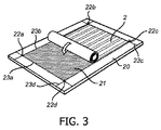
第1の例示的態様によれば、図3に概略的に示されるように、剛性支持板20は、テキスタイルキャリア2の拡がりに実質的に対応する領域21における取り外しが容易な粘着剤を備えている。さらに、剛性支持板20は、自動配置装置のアラインメントを可能にするための(しばしば基準とも称される)参照マーカ22a〜22dと、基準22a〜22dに対するテキスタイルキャリア2のアラインメントにおける補助のためのガイド23a〜23dとを備えている。
According to a first exemplary embodiment, as schematically shown in FIG. 3, the
図3において概略的に示されるように、テキスタイルキャリアは、ガイド23a〜23dにより位置決めされ、粘着剤を有する領域21に対して平らに押下される。図3に示されるように、テキスタイルキャリア2は、巻かれた状態からくるくると広げられてもよいが、もちろん、テキスタイルキャリアを剛性支持板20に取り付ける他の態様が可能である。
As shown schematically in FIG. 3, the textile carrier is positioned by the
テキスタイルキャリアが、ガイド23a〜23dにより位置決めされ、任意のシワを除去する(テキスタイルキャリア2の織物の引っ張りを多かれ少なかれ一般的には含み得る手続きの)ために剛性支持板20に対して平らに押下された後、テキスタイルキャリア支持板アセンブリは、導電性物質を付与するステップ102のための準備ができた状態となる。
The textile carrier is positioned by the
第2の例示的態様によれば、図4に概略的に示されるように、配置板26と、剛性支持板26からほぼ垂直に延在する互いに離れた4つの配列ピン27a〜27dとを有する剛性配列装置25を備えている。
According to a second exemplary embodiment, as shown schematically in FIG. 4, it has a
テキスタイルキャリア2は、図4から分かるように、配列ピン27a〜27dに対応する間隔で配置された、互いに離れた4つのテキスタイルキャリア開口部28a〜28dを有し、取り外し容易な粘着剤を(テキスタイルキャリア2に対向する側に)具備する剛性支持板20は、同様に配列ピン27a〜27dに対応する間隔で配置された、互いに離れた4つの支持板開口部31a〜31dを備えている。テキスタイルキャリア開口部は、テキスタイルを通じた配列ピンの貫通によって形成され得る。テキスタイルキャリアは、配列ピンが貫通すべき位置にマーカを持っていてもよい。
As can be seen from FIG. 4, the
図4に概略的に示されるように、テキスタイルキャリア2を剛性支持板に着脱可能に取り付ける上記ステップは、テキスタイルキャリア2を引っ張り、配列ピン27a〜27dをテキスタイルキャリア開口部28a〜28dへ挿入し、配列ピン27a〜27dを支持板開口部31a〜31dへ挿入することによって実行される。次いで、支持板20は、テキスタイルキャリア2が、支持板20と配列板26との間に挟み込まれるように、ひいては、剛性支持板20上に設けられた粘着剤に着脱可能に取り付けられるように、配列板26に対して押下される。
As schematically shown in FIG. 4, the above-described step of removably attaching the
これにより、テキスタイルキャリア支持板アセンブリは、導電性物質を付与するステップ102のための準備ができた状態となる。 The textile carrier support plate assembly is now ready for step 102 to apply the conductive material.
さらに、開示された実施形態に対する変形が、請求項に記載の発明を実施する際、図面、開示及び添付の請求項の研究から、当業者によって理解及び実施され得る。例えば、テキスタイルキャリアは、水平方向及び垂直方向における導体配線など、複数方向に延在する導体配線を有していてもよい。電子部品は、例えば、1つの水平方向の導体配線と1つの垂直方向の導体配線との間に接続されてもよい。さらに、接続パッド及び部品パッドは、矩形である必要はなく、任意の形状であってもよい。 Moreover, variations on the disclosed embodiments can be understood and implemented by those skilled in the art from studying the drawings, the disclosure, and the appended claims, when practicing the claimed invention. For example, the textile carrier may have conductor wiring extending in a plurality of directions, such as conductor wiring in the horizontal direction and the vertical direction. For example, the electronic component may be connected between one horizontal conductor wiring and one vertical conductor wiring. Furthermore, the connection pad and the component pad do not need to be rectangular, and may have any shape.
請求項中、「有する」なる用語は、他の要素又はステップを除外せず、不定冠詞「a」又は「an」は、複数であることを除外しない。特定の手段が相互に異なる従属項で言及されているという単なる事実は、これらの手段の組み合わせが好適に用いられ得ないということを示すものではない。 In the claims, the term “comprising” does not exclude other elements or steps, and the indefinite article “a” or “an” does not exclude a plurality. The mere fact that certain measures are recited in mutually different dependent claims does not indicate that a combination of these measured cannot be used to advantage.
Claims (13)
複数の導体配線を有するテキスタイルキャリアを供給するステップと、
前記テキスタイルキャリアを剛性支持板に着脱可能に取り付けるステップと、
接続パッドの複数のセットを前記テキスタイルキャリア上に形成するパターンで導電性物質を前記テキスタイルキャリアに供給するステップと、ここで、前記接続パッドの各セットは、電子部品の配置のための部品配置位置を定め、前記接続パッドの各セットは、前記複数の導体配線の1つと重なっている接続パッドを有し、前記接続パッドは、前記導体配線に対して平行な方向における接続パッド長と前記導体配線に対して直交する方向における接続パッド幅とを持ち、前記接続パッド幅は、前記導体配線に対して直交する前記方向における前記テキスタイルキャリアの幅の少なくとも1%であり、
前記電子部品を前記部品配置位置に自動的に置くステップと、
前記電子部品を前記テキスタイルキャリアに取り付けて、前記電子テキスタイルを形成するために、前記導電性物質を硬化させるステップと、
前記電子テキスタイルを前記剛性支持板から取り外すステップと、を有する、方法。 A method of manufacturing an electronic textile,
Supplying a textile carrier having a plurality of conductor wirings;
Removably attaching the textile carrier to a rigid support plate;
Supplying a conductive material to the textile carrier in a pattern that forms a plurality of sets of connection pads on the textile carrier, wherein each set of connection pads is a component placement position for placement of electronic components Each set of connection pads has a connection pad that overlaps one of the plurality of conductor wirings, the connection pads having a connection pad length in a direction parallel to the conductor wiring and the conductor wiring. A connection pad width in a direction orthogonal to the connection pad width, wherein the connection pad width is at least 1% of the width of the textile carrier in the direction orthogonal to the conductor wiring;
Automatically placing the electronic component at the component placement position;
Attaching the electronic component to the textile carrier and curing the conductive material to form the electronic textile;
Removing the electronic textile from the rigid support plate.
前記テキスタイルキャリアを引っ張るステップと、
前記剛性支持板上に設けられた接着層に対して前記テキスタイルキャリアを押し付けるステップと、を有する、請求項1乃至4のいずれか1項に記載の方法。 The step of detachably attaching includes:
Pulling the textile carrier;
5. The method according to claim 1, further comprising pressing the textile carrier against an adhesive layer provided on the rigid support plate.
前記着脱可能に取り付けるステップは、
配列板と前記配列板からほぼ垂直方向に延びている互いに離れた配列ピンとを有する剛性配列装置を供給するステップと、ここで、前記配列ピンは、前記剛性支持板の前記支持板開口部の配置に対応して配置され、
前記テキスタイルキャリアを引っ張るとともに、前記配列ピンが前記テキスタイルキャリアを貫くように、前記配列板上に前記テキスタイルキャリアを配置するステップと、
前記配列ピンに前記剛性支持板を配置するとともに、前記テキスタイルキャリアが前記剛性支持板に着脱可能に取り付けられるように、前記剛性支持板と前記配列板との間に前記テキスタイルキャリアを挟み込むステップと、を有する、請求項5記載の方法。 The rigid support plate has support plate openings separated from each other,
The step of detachably attaching includes:
Providing a rigid alignment device having an alignment plate and spaced apart alignment pins extending substantially vertically from the alignment plate, wherein the alignment pin is disposed in the support plate opening of the rigid support plate Are arranged corresponding to
Pulling the textile carrier and placing the textile carrier on the array plate such that the array pin penetrates the textile carrier;
Placing the rigid support plate on the alignment pin and sandwiching the textile carrier between the rigid support plate and the alignment plate so that the textile carrier is detachably attached to the rigid support plate; 6. The method of claim 5, comprising:
それぞれが前記複数の導体配線の1つと重なっており、前記導体配線に対して平行な方向における接続パッド長と前記導体配線に対して直交する方向における接続パッド幅とを持つ、複数の接続パッドと、
前記複数の接続パッドの1つを介して前記導体配線の1つに電気的に接続された第1の部品パッドをそれぞれ少なくとも持つ複数の電気部品と、を有し、
前記接続パッドの幅は、前記導体配線に対して直交する前記方向における前記テキスタイルキャリアの幅の少なくとも1%である、電子テキスタイル。 Textile carriers with multiple conductor wiring,
A plurality of connection pads, each overlapping one of the plurality of conductor wirings, having a connection pad length in a direction parallel to the conductor wiring and a connection pad width in a direction orthogonal to the conductor wiring; ,
A plurality of electrical components each having at least a first component pad electrically connected to one of the conductor wirings through one of the plurality of connection pads,
The width of the connection pad is at least 1% of the width of the textile carrier in the direction orthogonal to the conductor wiring.
Applications Claiming Priority (3)
| Application Number | Priority Date | Filing Date | Title |
|---|---|---|---|
| EP10177985 | 2010-09-21 | ||
| EP10177985.8 | 2010-09-21 | ||
| PCT/IB2011/053890 WO2012038849A1 (en) | 2010-09-21 | 2011-09-06 | Electronic textile and method of manufacturing an electronic textile |
Publications (2)
| Publication Number | Publication Date |
|---|---|
| JP2013537370A JP2013537370A (en) | 2013-09-30 |
| JP5867877B2 true JP5867877B2 (en) | 2016-02-24 |
Family
ID=44735988
Family Applications (1)
| Application Number | Title | Priority Date | Filing Date |
|---|---|---|---|
| JP2013528799A Expired - Fee Related JP5867877B2 (en) | 2010-09-21 | 2011-09-06 | Electronic textile and method for producing electronic textile |
Country Status (6)
| Country | Link |
|---|---|
| US (2) | US9148949B2 (en) |
| EP (1) | EP2620042A1 (en) |
| JP (1) | JP5867877B2 (en) |
| CN (1) | CN103109586B (en) |
| TW (1) | TW201213632A (en) |
| WO (1) | WO2012038849A1 (en) |
Families Citing this family (46)
| Publication number | Priority date | Publication date | Assignee | Title |
|---|---|---|---|---|
| EP2545542B1 (en) * | 2010-03-09 | 2014-01-08 | Koninklijke Philips N.V. | Light-emitting electronic textile with light-diffusing member |
| FR2962593B1 (en) * | 2010-07-06 | 2014-03-28 | Commissariat Energie Atomique | METHOD FOR ASSEMBLING A CHIP IN A FLEXIBLE SUBSTRATE |
| US9582072B2 (en) | 2013-09-17 | 2017-02-28 | Medibotics Llc | Motion recognition clothing [TM] with flexible electromagnetic, light, or sonic energy pathways |
| US9588582B2 (en) | 2013-09-17 | 2017-03-07 | Medibotics Llc | Motion recognition clothing (TM) with two different sets of tubes spanning a body joint |
| DE102013015015A1 (en) | 2013-09-07 | 2015-03-26 | Textilforschungsinstitut Thüringen-Vogtland e.V. | Method and device on a ribbon loom for weaving and fixing strips of mixed materials |
| US9826633B2 (en) * | 2013-11-05 | 2017-11-21 | Philips Lighting Holding B.V. | Electrically conducting textile device |
| DE102014200041A1 (en) * | 2014-01-07 | 2015-07-09 | Osram Gmbh | Textile luminous ceiling and method for producing a textile luminous ceiling |
| WO2015106998A1 (en) * | 2014-01-20 | 2015-07-23 | Koninklijke Philips N.V. | A lighting device and method for producing such device |
| US9575560B2 (en) | 2014-06-03 | 2017-02-21 | Google Inc. | Radar-based gesture-recognition through a wearable device |
| US9811164B2 (en) | 2014-08-07 | 2017-11-07 | Google Inc. | Radar-based gesture sensing and data transmission |
| US9921660B2 (en) | 2014-08-07 | 2018-03-20 | Google Llc | Radar-based gesture recognition |
| US10268321B2 (en) | 2014-08-15 | 2019-04-23 | Google Llc | Interactive textiles within hard objects |
| US9588625B2 (en) | 2014-08-15 | 2017-03-07 | Google Inc. | Interactive textiles |
| US9778749B2 (en) | 2014-08-22 | 2017-10-03 | Google Inc. | Occluded gesture recognition |
| US11169988B2 (en) | 2014-08-22 | 2021-11-09 | Google Llc | Radar recognition-aided search |
| US9600080B2 (en) | 2014-10-02 | 2017-03-21 | Google Inc. | Non-line-of-sight radar-based gesture recognition |
| US10016162B1 (en) | 2015-03-23 | 2018-07-10 | Google Llc | In-ear health monitoring |
| US9983747B2 (en) | 2015-03-26 | 2018-05-29 | Google Llc | Two-layer interactive textiles |
| US10310620B2 (en) | 2015-04-30 | 2019-06-04 | Google Llc | Type-agnostic RF signal representations |
| EP3289434A1 (en) | 2015-04-30 | 2018-03-07 | Google LLC | Wide-field radar-based gesture recognition |
| CN107430444B (en) | 2015-04-30 | 2020-03-03 | 谷歌有限责任公司 | RF-based micro-motion tracking for gesture tracking and recognition |
| US10088908B1 (en) | 2015-05-27 | 2018-10-02 | Google Llc | Gesture detection and interactions |
| US9693592B2 (en) | 2015-05-27 | 2017-07-04 | Google Inc. | Attaching electronic components to interactive textiles |
| FR3038919B1 (en) * | 2015-07-13 | 2018-11-09 | Ets A. Deschamps Et Fils | METHOD AND MACHINE FOR MANUFACTURING A WOVEN STRUCTURE |
| US10535278B2 (en) * | 2015-08-05 | 2020-01-14 | Myant, Inc. | Garment with stretch sensors |
| US10051898B2 (en) * | 2015-09-24 | 2018-08-21 | Loomia Technologies, Inc. | Smart soft good product, circuitry layer, and methods |
| US10817065B1 (en) | 2015-10-06 | 2020-10-27 | Google Llc | Gesture recognition using multiple antenna |
| US9837760B2 (en) * | 2015-11-04 | 2017-12-05 | Google Inc. | Connectors for connecting electronics embedded in garments to external devices |
| CN107105571B (en) * | 2016-02-23 | 2020-08-18 | 深圳富泰宏精密工业有限公司 | Flexible circuit board, manufacturing method thereof and electronic device with flexible circuit board |
| US10993635B1 (en) | 2016-03-22 | 2021-05-04 | Flextronics Ap, Llc | Integrating biosensor to compression shirt textile and interconnect method |
| US10492302B2 (en) | 2016-05-03 | 2019-11-26 | Google Llc | Connecting an electronic component to an interactive textile |
| US10297575B2 (en) * | 2016-05-06 | 2019-05-21 | Amkor Technology, Inc. | Semiconductor device utilizing an adhesive to attach an upper package to a lower die |
| US10175781B2 (en) | 2016-05-16 | 2019-01-08 | Google Llc | Interactive object with multiple electronics modules |
| US10579150B2 (en) | 2016-12-05 | 2020-03-03 | Google Llc | Concurrent detection of absolute distance and relative movement for sensing action gestures |
| US10236089B1 (en) | 2017-09-11 | 2019-03-19 | International Business Machines Corporation | Reducing environmental radon |
| US20190137091A1 (en) * | 2017-11-08 | 2019-05-09 | Rubelli S.P.A. | Fabric panel illuminated with optical fiber |
| US10426029B1 (en) | 2018-01-18 | 2019-09-24 | Flex Ltd. | Micro-pad array to thread flexible attachment |
| US10687421B1 (en) * | 2018-04-04 | 2020-06-16 | Flex Ltd. | Fabric with woven wire braid |
| US10772197B2 (en) * | 2018-04-24 | 2020-09-08 | Microsoft Technology Licensing, Llc | Electronically functional yarn |
| KR102009346B1 (en) * | 2018-08-14 | 2019-08-12 | (주)현대포멕스 | Lighting device with collapsible circuit wire and led, method of manufacturing the same |
| US10985484B1 (en) * | 2018-10-01 | 2021-04-20 | Flex Ltd. | Electronic conductive interconnection for bridging across irregular areas in a textile product |
| KR102661486B1 (en) * | 2018-10-22 | 2024-04-26 | 구글 엘엘씨 | Conductive fabric with custom placement conformal to the embroidery pattern |
| WO2021034209A1 (en) * | 2019-08-22 | 2021-02-25 | Têxteis Penedo Sa | Device for attaching a lighting component onto a textile structure,operating method and uses thereof |
| EP4079113A4 (en) * | 2019-12-18 | 2024-03-06 | Myant Inc. | Method of manufacturing textile with conductive yarns and integrated electronics |
| US11337312B2 (en) * | 2020-09-08 | 2022-05-17 | Palo Alto Research Center Incorporated | Systems and methods for bonding electronic components on substrates with rough surfaces |
| US11952087B2 (en) | 2020-12-11 | 2024-04-09 | Alessandra E. Myslinski | Smart apparel and backpack system |
Family Cites Families (17)
| Publication number | Priority date | Publication date | Assignee | Title |
|---|---|---|---|---|
| JP2001052856A (en) | 1999-08-09 | 2001-02-23 | Kawaguchiko Seimitsu Co Ltd | Electroluminescent element |
| DE10161527A1 (en) * | 2001-12-14 | 2003-07-03 | Infineon Technologies Ag | Construction and connection technology in textile structures |
| US7592276B2 (en) * | 2002-05-10 | 2009-09-22 | Sarnoff Corporation | Woven electronic textile, yarn and article |
| US7144830B2 (en) * | 2002-05-10 | 2006-12-05 | Sarnoff Corporation | Plural layer woven electronic textile, article and method |
| GB2396252A (en) * | 2002-10-01 | 2004-06-16 | Steven Leftly | Textile light system |
| JP2004228353A (en) * | 2003-01-23 | 2004-08-12 | Seiko Epson Corp | Wiring board and manufacturing method thereof, laminated wiring board, semiconductor device, circuit board, and electronic equipment |
| DE10307505B4 (en) * | 2003-02-21 | 2005-03-03 | Infineon Technologies Ag | A textile fabric structure, surface covering structure and method for determining a spacing of microelectronic elements of the textile fabric structure to at least one reference position |
| DE10325883A1 (en) * | 2003-06-06 | 2004-12-30 | Infineon Technologies Ag | Process for contacting conductive fibers |
| CN101036422B (en) | 2004-10-01 | 2010-04-14 | 东丽株式会社 | Long film circuit board, and production method and production device therefor |
| EP1727408A1 (en) * | 2005-05-13 | 2006-11-29 | Eidgenössische Technische Hochschule Zürich | Textile with conductor pattern and method for its production |
| WO2008001250A1 (en) | 2006-06-29 | 2008-01-03 | Koninklijke Philips Electronics N.V. | Pixelated electroluminescent textile |
| EP2020831A1 (en) * | 2007-07-31 | 2009-02-04 | Sefar AG | Method for manufacturing an electronic textile and textile substrate |
| CN102017814A (en) * | 2008-04-29 | 2011-04-13 | 皇家飞利浦电子股份有限公司 | Electronic textile |
| US9758907B2 (en) | 2008-09-22 | 2017-09-12 | Intel Corporation | Method and apparatus for attaching chip to a textile |
| TWM365363U (en) * | 2009-04-08 | 2009-09-21 | Fu-Biau Hsu | Illuminating textile article |
| US20110073353A1 (en) * | 2009-09-29 | 2011-03-31 | Tex-Ray Industrial Co., Ltd. | Conductive fabric and method for forming the same |
| FR2955972B1 (en) * | 2010-02-03 | 2012-03-09 | Commissariat Energie Atomique | METHOD FOR ASSEMBLING AT LEAST ONE CHIP WITH A FABRIC INCLUDING A CHIP DEVICE |
-
2011
- 2011-09-06 JP JP2013528799A patent/JP5867877B2/en not_active Expired - Fee Related
- 2011-09-06 EP EP11764320.5A patent/EP2620042A1/en not_active Withdrawn
- 2011-09-06 CN CN201180045519.6A patent/CN103109586B/en not_active Expired - Fee Related
- 2011-09-06 WO PCT/IB2011/053890 patent/WO2012038849A1/en active Application Filing
- 2011-09-06 US US13/822,642 patent/US9148949B2/en not_active Expired - Fee Related
- 2011-09-19 TW TW100133652A patent/TW201213632A/en unknown
-
2015
- 2015-09-18 US US14/857,907 patent/US9706648B2/en not_active Expired - Fee Related
Also Published As
| Publication number | Publication date |
|---|---|
| TW201213632A (en) | 2012-04-01 |
| CN103109586B (en) | 2017-02-15 |
| CN103109586A (en) | 2013-05-15 |
| US20130176737A1 (en) | 2013-07-11 |
| US20160014890A1 (en) | 2016-01-14 |
| JP2013537370A (en) | 2013-09-30 |
| US9148949B2 (en) | 2015-09-29 |
| EP2620042A1 (en) | 2013-07-31 |
| RU2013118262A (en) | 2014-10-27 |
| WO2012038849A1 (en) | 2012-03-29 |
| US9706648B2 (en) | 2017-07-11 |
Similar Documents
| Publication | Publication Date | Title |
|---|---|---|
| JP5867877B2 (en) | Electronic textile and method for producing electronic textile | |
| CN109996911B (en) | Intelligent yarn and method for manufacturing yarn containing electronic device | |
| CN107002318B (en) | Fabric with embedded electronic components | |
| WO2010058360A1 (en) | Textile electronic arrangement | |
| JP5868882B2 (en) | Method of manufacturing a device having a transponder antenna connected to a contact pad and the resulting device | |
| CN105830541B (en) | Conductive spinning product equipment | |
| CN108140634B (en) | Method for surface mounting a component | |
| CN104303604B (en) | Base, assembly including base, assembly method and assembly device | |
| CN1976804A (en) | Perforated functional textile structures | |
| JP2011519177A (en) | Electronic textile | |
| TW201010536A (en) | Flex-rigid wiring board and electronic device | |
| KR101199483B1 (en) | Textile-type electronic component package and method, method for mounting the same on textile | |
| CN103155143A (en) | Waterfall wire bonding | |
| BRPI0820752B1 (en) | method of producing a device comprising at least two distinct components which are interconnected by interconnect wires and device thus obtained | |
| KR20060048523A (en) | Cotton-Mount Coil Package and Manufacturing Method Thereof | |
| KR20180034160A (en) | Electric conduction planar element with insert type electric cable and manufacture method thereof | |
| RU2587927C2 (en) | Electronic fabric and method of making fabric | |
| CN102181987A (en) | Novel fabric display | |
| JP4525170B2 (en) | Manufacturing method of flexible printed wiring board and flexible printed wiring board manufactured using the same | |
| KR20110112154A (en) | Electric conduction body and manufacturing method thereof | |
| KR20140021864A (en) | Method of providing additional plate for adhering onto printed circuit board | |
| CN113450672B (en) | Transparent display screen | |
| JP2015162521A (en) | Adhesive coating method and method for manufacturing mounting substrate | |
| CN117166158A (en) | Knitting method of electric embroidery thread | |
| KR20230018858A (en) | LED textile fabrication methods and phototherapy wearables using the same |
Legal Events
| Date | Code | Title | Description |
|---|---|---|---|
| A621 | Written request for application examination |
Free format text: JAPANESE INTERMEDIATE CODE: A621 Effective date: 20140902 |
|
| A977 | Report on retrieval |
Free format text: JAPANESE INTERMEDIATE CODE: A971007 Effective date: 20150528 |
|
| A131 | Notification of reasons for refusal |
Free format text: JAPANESE INTERMEDIATE CODE: A131 Effective date: 20150602 |
|
| RD02 | Notification of acceptance of power of attorney |
Free format text: JAPANESE INTERMEDIATE CODE: A7422 Effective date: 20151005 |
|
| TRDD | Decision of grant or rejection written | ||
| A01 | Written decision to grant a patent or to grant a registration (utility model) |
Free format text: JAPANESE INTERMEDIATE CODE: A01 Effective date: 20151201 |
|
| A521 | Request for written amendment filed |
Free format text: JAPANESE INTERMEDIATE CODE: A821 Effective date: 20151225 |
|
| A61 | First payment of annual fees (during grant procedure) |
Free format text: JAPANESE INTERMEDIATE CODE: A61 Effective date: 20151225 |
|
| R150 | Certificate of patent or registration of utility model |
Ref document number: 5867877 Country of ref document: JP Free format text: JAPANESE INTERMEDIATE CODE: R150 |
|
| S111 | Request for change of ownership or part of ownership |
Free format text: JAPANESE INTERMEDIATE CODE: R313113 |
|
| R350 | Written notification of registration of transfer |
Free format text: JAPANESE INTERMEDIATE CODE: R350 |
|
| LAPS | Cancellation because of no payment of annual fees |