JP5847995B2 - Semiconductor device - Google Patents
Semiconductor device Download PDFInfo
- Publication number
- JP5847995B2 JP5847995B2 JP2010102385A JP2010102385A JP5847995B2 JP 5847995 B2 JP5847995 B2 JP 5847995B2 JP 2010102385 A JP2010102385 A JP 2010102385A JP 2010102385 A JP2010102385 A JP 2010102385A JP 5847995 B2 JP5847995 B2 JP 5847995B2
- Authority
- JP
- Japan
- Prior art keywords
- voltage
- potential
- buffer amplifier
- output
- input
- Prior art date
- Legal status (The legal status is an assumption and is not a legal conclusion. Google has not performed a legal analysis and makes no representation as to the accuracy of the status listed.)
- Active
Links
- 239000004065 semiconductor Substances 0.000 title claims description 39
- 230000002159 abnormal effect Effects 0.000 claims description 4
- 238000012544 monitoring process Methods 0.000 description 51
- 238000005259 measurement Methods 0.000 description 18
- 238000010586 diagram Methods 0.000 description 15
- 102100039435 C-X-C motif chemokine 17 Human genes 0.000 description 13
- 101000889048 Homo sapiens C-X-C motif chemokine 17 Proteins 0.000 description 13
- 239000003990 capacitor Substances 0.000 description 10
- 230000003071 parasitic effect Effects 0.000 description 8
- 238000001514 detection method Methods 0.000 description 7
- 230000007423 decrease Effects 0.000 description 3
- 229920006395 saturated elastomer Polymers 0.000 description 3
- 230000015556 catabolic process Effects 0.000 description 2
- 238000006243 chemical reaction Methods 0.000 description 2
- 230000037361 pathway Effects 0.000 description 2
- 230000000694 effects Effects 0.000 description 1
- 238000000034 method Methods 0.000 description 1
Images


Classifications
-
- G—PHYSICS
- G01—MEASURING; TESTING
- G01R—MEASURING ELECTRIC VARIABLES; MEASURING MAGNETIC VARIABLES
- G01R31/00—Arrangements for testing electric properties; Arrangements for locating electric faults; Arrangements for electrical testing characterised by what is being tested not provided for elsewhere
- G01R31/36—Arrangements for testing, measuring or monitoring the electrical condition of accumulators or electric batteries, e.g. capacity or state of charge [SoC]
- G01R31/382—Arrangements for monitoring battery or accumulator variables, e.g. SoC
- G01R31/3835—Arrangements for monitoring battery or accumulator variables, e.g. SoC involving only voltage measurements
-
- G—PHYSICS
- G01—MEASURING; TESTING
- G01R—MEASURING ELECTRIC VARIABLES; MEASURING MAGNETIC VARIABLES
- G01R31/00—Arrangements for testing electric properties; Arrangements for locating electric faults; Arrangements for electrical testing characterised by what is being tested not provided for elsewhere
- G01R31/36—Arrangements for testing, measuring or monitoring the electrical condition of accumulators or electric batteries, e.g. capacity or state of charge [SoC]
- G01R31/396—Acquisition or processing of data for testing or for monitoring individual cells or groups of cells within a battery
-
- H—ELECTRICITY
- H02—GENERATION; CONVERSION OR DISTRIBUTION OF ELECTRIC POWER
- H02J—CIRCUIT ARRANGEMENTS OR SYSTEMS FOR SUPPLYING OR DISTRIBUTING ELECTRIC POWER; SYSTEMS FOR STORING ELECTRIC ENERGY
- H02J7/00—Circuit arrangements for charging or depolarising batteries or for supplying loads from batteries
- H02J7/0013—Circuit arrangements for charging or depolarising batteries or for supplying loads from batteries acting upon several batteries simultaneously or sequentially
- H02J7/0014—Circuits for equalisation of charge between batteries
- H02J7/0016—Circuits for equalisation of charge between batteries using shunting, discharge or bypass circuits
Landscapes
- Physics & Mathematics (AREA)
- General Physics & Mathematics (AREA)
- Measurement Of Current Or Voltage (AREA)
- Charge And Discharge Circuits For Batteries Or The Like (AREA)
- Secondary Cells (AREA)
Description
本発明は、半導体装置、特に電池監視用の半導体装置に関するものである。
The present invention relates to a semiconductor equipment, and in particular relates to a semiconductor equipment for battery monitoring.
一般に、直列に接続された複数の電池の監視・制御を行うための半導体装置がある。このような半導体装置として、例えば車両等に搭載される電池を監視・制御するための電池監視IC(Integral Circuit)が知られている。例えば、特許文献1には、電気自動車、あるいはハイブリッド電気自動車用の蓄電池等として用いられる高エネルギーの蓄電器を複数個直列に接続したものを制御する蓄電装置及びその制御方法が記載されている。
In general, there is a semiconductor device for monitoring and controlling a plurality of batteries connected in series. As such a semiconductor device, for example, a battery monitoring IC (Integral Circuit) for monitoring and controlling a battery mounted on a vehicle or the like is known. For example,
従来の電池監視ICの概略構成の一例を図9に示す。図9に示した電池114を監視・制御するための従来の電池監視IC100は、セル選択SW118及びアナログレベルシフタ122を含んで構成されている。
An example of a schematic configuration of a conventional battery monitoring IC is shown in FIG. A conventional
電池114は、直列に接続された5個の電池セルVc1〜Vc5を含んでおり、電池セルVc1の負極は、GND(グランド)に接続されている。また、電池セルVc5の正極は、電池監視IC100の電源VCCに接続されている。電池114の両端電圧V0〜V5は、各々のLPF(ローパスフィルタ)116を介して、電池監視IC100のセル選択SW118の入力に接続されている。セル選択SW118の出力はアナログレベルシフタ122に接続されている。また、アナログレベルシフタ122は、検出抵抗R1〜R4、アンプ136、ダミースイッチSWA、SWBを備えて構成されている。ダミースイッチSWA、SWBは、セル選択SW118に含まれる各スイッチング素子SW0〜SW5と同じオン抵抗を持ったダミースイッチング素子であり、常時オン状態になっている。また、本実施の形態のアナログレベルシフタ122には、ダミー抵抗RD1、RD2が接続されている。ダミー抵抗RD1、RD2は、LPF116の抵抗Rf01〜Rf51で発生する誤差をキャンセルするためのダミー抵抗素子であり、LPF116の抵抗Rf01〜Rf51と抵抗値が同じ抵抗素子である。
The battery 114 includes five battery cells Vc1 to Vc5 connected in series, and the negative electrode of the battery cell Vc1 is connected to GND (ground). Further, the positive electrode of the battery cell Vc5 is connected to the power supply VCC of the
従来の電池監視IC100による電池114の電池電圧の測定について図10、11を参照して説明する。電池セルVc5の電圧値を測定する場合、セル選択SW118のスイッチング素子SW5、SW4_1がオン状態になり、その他のスイッチング素子がオフ状態になる。検出抵抗R1〜R4の抵抗値が同一(R1=R2=R3=R4)、スイッチング素子SW5、SW4_1、SWA、SWBのオン抵抗をRSWとすると、電池セルVc5の電圧Vc5=V5−V4はアナログレベルシフタ122によって電圧変換され、Vout=Vc5になり、GND基準の電圧に変換される。
Measurement of the battery voltage of the battery 114 by the conventional
同様に、電池セルVc4の電圧を測定する場合は、セル選択SW118のスイッチング素子SW4_2、SW3_1がオン状態になり、その他のスイッチング素子がオフ状態になり、アナログレベルシフタ122よって電圧変換されて、Vout=Vc4になる。電池セルVc3の電圧を測定する場合は、セル選択SW118のスイッチング素子SW3_2、SW2_1がオン状態になり、その他のスイッチング素子がオフ状態になり、アナログレベルシフタ122よって電圧変換されて、Vout=Vc3になる。電池セルVc2の電圧を測定する場合、セル選択SW118のスイッチング素子SW2_2、SW1_1がオン状態になり、その他のスイッチング素子がオフ状態になり、アナログレベルシフタ122よって電圧変換されて、Vout=Vc2になる。電池セルVc1の電圧を測定する場合、セル選択SW118のスイッチング素子SW1_2、SW0がオン状態になり、その他のスイッチング素子がオフ状態になり、アナログレベルシフタ122よって電圧変換されて、Vout=Vc1になる。
Similarly, when measuring the voltage of the battery cell Vc4, the switching elements SW4_2 and SW3_1 of the cell selection SW118 are turned on, the other switching elements are turned off, and voltage conversion is performed by the
セル選択SW118の各スイッチング素子SW0〜SW5は、MOS(モス)トランジスタで構成されているため、各々のスイッチング素子SW0〜SW5−GND間に寄生容量C0〜C5が発生している。そのため、図11に示すように、電池セルVc5の電圧値の測定時にスイッチング素子SW5、SW4_1をオン状態にした直後、LPF116のコンデンサCf5の電荷が寄生容量C41、C5に移動するため、移動量に応じて、電圧V41、V51、Voutが落ち込む。セル選択SW118の寄生容量が大きいと、移動する電荷の量が増加するため、電圧の落ち込みが大きくなる。
Since the switching elements SW0 to SW5 of the cell selection SW118 are composed of MOS transistors, parasitic capacitances C0 to C5 are generated between the switching elements SW0 to SW5 to GND. Therefore, as shown in FIG. 11, the charge of the capacitor Cf5 of the
また、電池セルVc5の電圧値の測定時にスイッチング素子SW5、SW4_1をオン状態にした直後は、アナログレベルシフタ122の検出抵抗R1〜R4に流れる電流は、LPF116の抵抗Rf0〜Rf5、及びコンデンサCf0〜Cf5を介して電池セルVc1〜Vc5から供給される(図10、太線参照)ため、さらに、電圧が落ち込む。特にLPF116の抵抗Rf0〜Rf5の抵抗値が大きいと電圧の落ち込みは大きい。
Further, immediately after the switching elements SW5 and SW4_1 are turned on when measuring the voltage value of the battery cell Vc5, the currents flowing through the detection resistors R1 to R4 of the
このように落ち込んだ電圧は、LPF116の時定数で復帰するため、出力電圧Voutが安定するまでに時間がかかる。LPF116の時定数が大きいほど、安定するまでの時間が長くなる。
Since the voltage that has dropped in this way is restored by the time constant of the
このように、従来の電池監視IC100による電池電圧の測定では、アナログレベルシフタ122の出力が安定するまでに時間がかかるため、測定時間が長くなるという問題があった。
As described above, in the measurement of the battery voltage by the conventional
本発明は、上述した問題を解決するために提案されたものであり、電池電圧の測定時間を短くすることができる半導体装置を提供することを目的とする。
The present invention has been proposed to solve the above problems, and an object thereof is to provide a semiconductor equipment that can shorten the measurement time of the battery voltage.
上記目的を達成するために、請求項1に記載の半導体装置は、直列に接続された複数の電池セルの各々の一端の電位と他端の電位とが、容量手段を備えたフィルタを介して入力され、選択された電池セルの前記一端の電位と前記他端の電位との差分に基づいて前記選択された電池セルの電圧を検出する半導体装置であって、MOSトランジスタであり、前記複数の電池セルの各々の一端と前記フィルタを介して接続されて、前記選択された電池セルの一端の電位を出力する第1のセル選択スイッチと、MOSトランジスタであり、前記複数の電池セルの各々の他端と前記フィルタを介して接続されて、前記選択された電池セルの他端の電位を出力する第2のセル選択スイッチと、第1のトランジスタを備え、前記選択された電池セルの一端の電位が前記第1のセル選択スイッチから前記第1のトランジスタのゲートに入力されて前記一端の電位に基づく第1の電圧を出力する第1のバッファアンプと、第2のトランジスタを備え、前記選択された電池セルの他端の電位が前記第2のセル選択スイッチから前記第2のトランジスタのゲートに入力されて前記他端の電位に基づく第2の電圧を出力する第2のバッファアンプと、前記第1の電圧が第1の抵抗を介して入力され、一端がグランドに接続される第2の抵抗の他端に接続される非反転端子と、前記第2の電圧が第3の抵抗を介して入力され、第4の抵抗を介して自身が出力した出力信号が入力される反転端子とを備えたアナログレベルシフタを含む差分出力手段と、前記直列に接続された複数の電池セルから供給される電源電圧が前記第1のトランジスタを飽和領域で動作するための電圧値よりも低い場合に、前記電源電圧を、前記第1のトランジスタが前記飽和領域で動作するための電圧値に昇圧し、また、前記電源電圧が前記第2のトランジスタを飽和領域で動作させるための電圧値よりも低い場合に、前記電源電圧を、前記第2のトランジスタが前記飽和領域で動作するための電圧値に昇圧し、昇圧した電圧を前記第1のバッファアンプ及び前記第2のバッファアンプに供給する昇圧手段と、を有することを特徴とする。
請求項2に記載の半導体装置は、請求項1に記載の半導体装置において、前記昇圧手段 は、前記電源電圧が前記第1のトランジスタを飽和領域で動作するための電圧値以上の場 合、及び前記電源電圧が前記第2のトランジスタを飽和領域で動作させるための電圧値以 上の場合は、前記電源電圧の昇圧を行わない。
In order to achieve the above object, in the semiconductor device according to
The semiconductor device according to
請求項3に記載の半導体装置は、請求項1または請求項2に記載の半導体装置において、前記一端の電位が前記各々の電池セルの上位電位であり、前記他端の電位が前記各々の電池セルの下位電位であり、前記第1の電圧が前記差分出力手段の非反転端子に入力され、前記第2の電圧が前記差分出力手段の反転端子に入力されることを特徴とする。
The semiconductor device according to
請求項4に記載の半導体装置は、請求項1乃至請求項3のいずれか1項に記載の半導体装置において、前記第1のバッファアンプの入力端子と出力端子との接続を制御する第1のスイッチ素子と、前記第2のバッファアンプの入力端子と出力端子との接続を制御する第2のスイッチ素子と、を備え、前記第1のバッファアンプの入力端子と出力端子とを前記第1のスイッチ素子で接続せず且つ前記第2のバッファアンプの入力端子と出力端子とを前記第2のスイッチ素子で接続しない状態で前記差分出力手段によって得られる前記第1の電圧と前記第2の電圧との第1の差分電圧と、前記第1のバッファアンプの入力端子と出力端子とを前記第1のスイッチ素子で接続し且つ前記第2のバッファアンプの入力端子と出力端子とを前記第2のスイッチ素子で接続した状態で前記差分出力手段によって得られる前記選択された電池セルの前記一端の電位と前記他端の電位との差分電圧である第2の差分電圧と、を比較し、前記第1の差分電圧と前記第2の差分電圧とが一致した場合には前記第1のバッファアンプ及び前記第2のバッファアンプが正常に動作していると判定し、前記第1の差分電圧と前記第2の差分電圧とが一致しなかった場合には前記第1のバッファアンプ及び前記第2のバッファアンプが異常であると判定することを特徴とする。
A semiconductor device according to a fourth aspect of the present invention is the semiconductor device according to any one of the first to third aspects, wherein the first buffer amplifier controls the connection between the input terminal and the output terminal of the first buffer amplifier. A switch element, and a second switch element that controls connection between an input terminal and an output terminal of the second buffer amplifier, and the input terminal and the output terminal of the first buffer amplifier are connected to the first buffer amplifier. The first voltage and the second voltage obtained by the differential output means without being connected by a switch element and without connecting the input terminal and the output terminal of the second buffer amplifier by the second switch element. Are connected to the input terminal and the output terminal of the first buffer amplifier by the first switch element, and the input terminal and the output terminal of the second buffer amplifier are connected to the second No A second differential voltage that is a differential voltage between the potential at the one end and the potential at the other end of the selected battery cell obtained by the differential output means in a state of being connected by a switch element, and When the first differential voltage and the second differential voltage match, it is determined that the first buffer amplifier and the second buffer amplifier are operating normally, and the first differential voltage and When the second differential voltage does not match, it is determined that the first buffer amplifier and the second buffer amplifier are abnormal.
請求項5に記載の半導体装置は、請求項1乃至請求項4のいずれか1項に記載の半導体装置において、前記直列に接続された複数の電池セルのうち、前記他端の電位がグランドに接続された電池セルが選択された場合には、前記選択された電池セルのものとして検出する電圧を、前記差分出力手段から出力される電圧に代えて、前記一端の電位とする切替素子を備えた。
The semiconductor device according to claim 5 is the semiconductor device according to any one of
本発明によれば、電池電圧の測定時間を短くすることができる、という効果を奏する。 According to the present invention, there is an effect that the measurement time of the battery voltage can be shortened.
[第1の実施の形態] [First Embodiment]
以下、図面を参照して本発明の第1の実施の形態の電池監視用の半導体装置について詳細に説明する。 The battery monitoring semiconductor device according to the first embodiment of the present invention will be described below in detail with reference to the drawings.
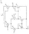
図1に、本実施の形態の半導体装置(電池監視IC)の概略構成の一例の回路図を示す。本実施の形態の電池監視IC10は、セル選択SW18、バッファアンプ20、及びアナログレベルシフタ22を備えて構成されている。バッファアンプ20は、バッファアンプ30及びバッファアンプ32を含んで構成されており、アナログレベルシフタ22は、検出抵抗R1、R2、R3、R4及びアンプ36により差動増幅回路を構成している。
FIG. 1 shows a circuit diagram of an example of a schematic configuration of a semiconductor device (battery monitoring IC) of the present embodiment. The
電池14は、直列に接続された5個の電池セルVc1〜Vc5を含んでおり、電池セルVc1の負極は、GNDに接続されている。また、電池セルVc5の正極は、電池監視IC10の電源に接続されている。電池セルVc1〜Vc5各々の両端は、両端電圧V0〜V5が入力されるようにコンデンサCf1〜Cf5、及び抵抗Rf0〜Rf5により構成されるLPF16を介して、電池監視IC10のセル選択SW18のスイッチング素子SW0〜SW5に接続されている。
The battery 14 includes five battery cells Vc1 to Vc5 connected in series, and the negative electrode of the battery cell Vc1 is connected to GND. Further, the positive electrode of the battery cell Vc5 is connected to the power source of the
セル選択SW18は、各電池セルVc1〜Vc5を選択するためのスイッチング素子SW0〜SW5を含んで構成されている。本実施の形態では、スイッチング素子SW0〜SW5は、全て同様の構造をしており、高耐圧のMOSトランジスタにより構成されている。本実施の形態のスイッチング素子SW0〜SW5の具体的一例の回路図を図2に示す。本実施の形態のスイッチング素子SW0〜SW5は、NMOSトランジスタ70、PMOSトランジスタ72、及び論理否定回路74を含んで構成されている。論理否定回路74に入力される制御信号がハイレベルの場合は、NMOSトランジスタ70及びPMOSトランジスタ72がオン状態になり、LPF16からバッファアンプ20に電圧が出力される。一方、論理否定回路74に入力される制御信号がローレベルの場合は、NMOSトランジスタ70及びPMOSトランジスタ72がオフ状態になり、LPF16からバッファアンプ20に電圧が出力されない。なおスイッチング素子SW0〜SW5は、高耐圧トランジスタにより構成されるものであればこれに限定されず、その他の構成であってもよい。
The cell selection SW18 includes switching elements SW0 to SW5 for selecting the battery cells Vc1 to Vc5. In the present embodiment, the switching elements SW0 to SW5 all have the same structure, and are constituted by high breakdown voltage MOS transistors. FIG. 2 shows a circuit diagram of a specific example of the switching elements SW0 to SW5 of the present embodiment. The switching elements SW0 to SW5 of the present embodiment are configured to include an
セル選択SW18の出力は、バッファアンプ20の非反転端子に接続されている。本実施の形態では、セル選択SW18のスイッチング素子SW0、SW1_1、SW2_1、SW3_1、SW4_1がバッファアンプ32の非反転入力端子に接続されており、スイッチング素子SW1_2、SW2_2、SW3_2、SW4_2、SW5がバッファアンプ30の非反転入力端子に接続されている。なお、バッファアンプ30、32の反転端子には、各々出力が接続(負帰還)されている。
The output of the
本実施の形態では、バッファアンプ30、32は、同様の構造をしており、高耐圧のMOSトランジスタにより構成されている。本実施の形態のバッファアンプ30、32の具体的一例の回路図を図3に示す。本実施の形態のバッファアンプ30、32は、PMOSトランジスタ80、82、84、86、コンデンサ88、及びNMOSトランジスタ90、92、94を含んで構成されている。本実施の形態では、非反転端子から入力された電圧Vx、Vyと電圧値が同じ電圧Vx1、Vy1(Vx=Vx1、Vy=Vy1)が出力端子から出力される。なおバッファアンプ30、32は、高耐圧トランジスタにより構成されるものであればこれに限定されず、その他の構成であってもよい。
In the present embodiment, the
バッファアンプ20の出力は、アナログレベルシフタ22に接続されている。本実施の形態では、バッファアンプ30の出力(Vx1)は、検出抵抗R1を介してアンプ36の非反転端子に接続されており、バッファアンプ32の出力(Vy1)は、アンプ36の反転端子に接続されている。
The output of the
アナログレベルシフタ22は、セル選択SW18により選択された電池セルの両端電圧の電圧値の差をVoutとして電池監視IC10の外部に出力する。本実施の形態のアナログレベルシフタ22の具体的一例としては、バッファアンプ30、32と同様の構造(図3参照)を有したアンプ36、及び抵抗値が同一の検出抵抗R1〜R4(R1=R2=R3=R4)を備えた構成が挙げられる。
The
本実施の形態の電池監視IC10による電池セルVc1〜Vc5の電池電圧の測定について図4、5を参照して説明する。電池セルVc5の電圧値(V5−V4=Vc5)を測定する場合、セル選択SW18のスイッチング素子SW5、SW4_1がオン状態になり、その他のスイッチング素子がオフ状態になる。バッファアンプ30、32の入力インピーダンスが高いため、電流による抵抗Rf4、Rf5、セル選択SW18(スイッチング素子SW4_1、SW5)による電圧降下がないため、電圧Vx=V5、電圧Vy=V4になる。従って、アナログレベルシフタ22の出力Voutは、V5−V4=Vc5となり、グランド基準の電圧に変換されて外部に出力される。
Measurement of the battery voltage of the battery cells Vc1 to Vc5 by the
なお同様に、電池セルVc4の電圧を測定する場合は、セル選択SW18のスイッチング素子SW4_2、SW3_1がオン状態になり、その他のスイッチング素子がオフ状態になり、アナログレベルシフタ22からVout=Vc4が出力される。電池セルVc3の電圧を測定する場合は、セル選択SW18のスイッチング素子SW3_2、SW2_1がオン状態になり、その他のスイッチング素子がオフ状態になり、アナログレベルシフタ22からVout=Vc3が出力される。電池セルVc2の電圧を測定する場合、セル選択SW18のスイッチング素子SW2_2、SW1_1がオン状態になり、その他のスイッチング素子がオフ状態になり、アナログレベルシフタ22からVout=Vc2が出力される。電池セルVc1の電圧を測定する場合、セル選択SW18のスイッチング素子SW1_2、SW0がオン状態になり、その他のスイッチング素子がオフ状態になり、アナログレベルシフタ22からVout=Vc1が出力される。
Similarly, when measuring the voltage of the battery cell Vc4, the switching elements SW4_2 and SW3_1 of the cell selection SW18 are turned on, the other switching elements are turned off, and Vout = Vc4 is output from the
上述のようにして電池監視IC10から出力された出力電圧Voutの電圧値を測定することにより、電池セルVc1〜Vc5の電池電圧の測定が行われる。例えば、車等に搭載される電池(電気自動車やハイブリッド電気自動車用の蓄電池等)の測定に用いられる。
By measuring the voltage value of the output voltage Vout output from the
本実施の形態では、入力インピーダンスが高いバッファアンプ30、32がセル選択SW18の出力に接続されているため、電池セルVc5の電池電圧を測定する場合、図4に太線で示すように電流が流れる。このように本実施の形態では、従来の電池監視IC100による電池電圧の測定の際の電流の流れを示す図10と比較するとわかるように、電池セルVc1〜Vc4からLPF16の抵抗Rf0〜Rf3及びコンデンサCf1〜Cf4を介して電流が流れるのを抑制する。従って、本実施の形態では、従来に比べて、セル選択SW18のスイッチング素子SW4_1、SW5に流れる電流量が減少する。そのため、スイッチング素子SW4_1、SW5を構成するMOSトランジスタを小型化することができる。本実施の形態では、具体的一例として、MOSトランジスタのゲート幅やゲート長を小さくすることにより、小型化する。MOSトランジスタが物理的に小型化されるため、スイッチング素子SW4_1、SW5の寄生容量C41、C5が小さくなる。
In this embodiment, since the
寄生容量が小さくなると、セル選択SW18をオンした直後のコンデンサCf5から寄生容量へ移動する電荷の移動量が少なくなる。また図4に示すように検出抵抗R1〜R4に流れる電流は、バッファアンプ30、32から供給される。すなわち、従来と異なり、LPF16の抵抗Rf0〜Rf5、及びコンデンサCf0〜Cf5を介して電池セルVc1〜Vc5から供給されない。従って、図5に示すように、電池セル電圧測定時の電圧の落ち込みが少ないので、出力電圧Voutが安定していない状態で測定しても精度よく(規格を満足できる精度)測定できる。
When the parasitic capacitance is reduced, the amount of charge transferred from the capacitor Cf5 immediately after the
具体的一例としては、スイッチング素子SW4_1、SW5のオン電圧が60V、オフ電圧が0Vの場合に、電圧V51、V41の落ち込みは3mV、出力電圧Voutの落ち込みは6mVになり、規格内で測定できるセル電圧測定時間は500μsになる。 As a specific example, when the ON voltage of the switching elements SW4_1 and SW5 is 60V and the OFF voltage is 0V, the drop of the voltages V51 and V41 is 3mV, and the drop of the output voltage Vout is 6mV. The voltage measurement time is 500 μs.
なお、ここでは、電池セルVc5の電池電圧を測定する場合について詳細に説明したが、その他の電池セルVc1〜Vc4の電池電圧を測定する場合についても上記と同様の理由により、セル選択SW18のスイッチング素子SW0〜SW4_2を小さくすることができるため、寄生容量を小さくすることができ、従って、電池セル電圧測定時の電圧の落ち込みが少ないので、出力電圧Voutを規格内で測定できる時間まで短くすることができる。
Here, the case where the battery voltage of the battery cell Vc5 is measured has been described in detail. However, when the battery voltages of the other battery cells Vc1 to Vc4 are measured, the switching of the
以上説明したように、本実施の形態の電池監視IC10によれば、セル選択SW18のスイッチング素子SW0〜SW5により選択された電池セルの正極側の電圧がバッファアンプ20のバッファアンプ30の非反転端子に入力され、バッファアンプ30から出力された電圧Vx1がアナログレベルシフタ22のアンプ36の非反転端子に入力される。また、選択された電池の負極側の電圧がバッファアンプ32の非反転端子に入力され、バッファアンプ32から出力された電圧Vy1がアンプ36の反転端子に入力される。アナログレベルシフタ22からは、電圧Vx1と電圧Vy1の電圧値の差がVoutとして出力される。従って、電池電圧の両端電圧の差がアナログレベルシフタ22からVoutとして出力される。
As described above, according to the
このように本実施の形態では、入力インピーダンスが高いバッファアンプ30、32を介してセル選択SW18からアナログレベルシフタ22に電圧が入力されるため、セル選択SW18のスイッチング素子SW0〜SW5に流れる電流を抑制し、電流量を従来よりも少なくすることができるため、スイッチング素子SW0〜SW5を構成するMOSトランジスタの物理的大きさを小さくすることができる。これにより、セル選択SW18の寄生容量C0〜C5を小さくすることができる。
As described above, in the present embodiment, since the voltage is input from the cell selection SW18 to the
従って、電池セルVc1〜Vc5の電池電圧の測定時にアナログレベルシフタ22から出力される電圧Voutの落ち込みを少なくすることができるため、出力電圧Voutを規格内で測定できる時間まで短くすることができる。
Therefore, since the drop of the voltage Vout output from the
また、本実施の形態では、バッファアンプ20のバッファアンプ30、32、及びアナログレベルシフタ22のアンプ36の駆動電源として、電池14の電池セルVc5の正極から電源電圧VCCを供給している。これにより、バッファアンプ30、32を駆動するための新たな電源を備える構成としなくてよいため、電池監視IC10のチップ面積の増大を抑制することができる。
In the present embodiment, the power supply voltage VCC is supplied from the positive electrode of the battery cell Vc5 of the battery 14 as the drive power for the
[第2の実施の形態] [Second Embodiment]
以下、図面を参照して本発明の第2の実施の形態の半導体装置である電池監視ICについて詳細に説明する。図6に、本実施の形態の半導体装置(電池監視IC)の概略構成の一例の回路図を示す。本実施の形態の電池監視IC40は第1の実施の形態の電池監視IC10と略同一の構成であるため、同一部分には同一符号を付し、詳細な説明を省略する。
Hereinafter, a battery monitoring IC which is a semiconductor device according to a second embodiment of the present invention will be described in detail with reference to the drawings. FIG. 6 shows a circuit diagram of an example of a schematic configuration of the semiconductor device (battery monitoring IC) of the present embodiment. Since the
本実施の形態の電池監視IC40は、昇圧回路42を備えている。昇圧回路42は、電池14の電池セルVc5の正極から供給される電源電圧VCCを所定の電圧VCC1(VCC<VCC1)に昇圧し、昇圧した電圧VCC1をバッファアンプ20のバッファアンプ30、32の駆動電源電圧として供給する。
The
第1の実施の形態の電池監視IC10では、電池セルVc5の電池電圧を測定する場合、電池セルVc5の正極側に接続されているバッファアンプ30の入力電圧VxがVx=V5=VCCとなる。このようにバッファアンプ30の入力電圧の電圧値とバッファアンプ30の電源電圧の電圧値とが同じく電圧VCCになるため、バッファアンプ30内のMOSトランジスタが非飽和領域で動作し、バッファアンプ30の出力のオフセット電圧が大きくなる。オフセット電圧の影響により、出力電圧Voutによる電池電圧の測定精度が低下する場合がある。
In the
本実施の形態では、電圧VCCを昇圧回路42により、バッファアンプ30内のMOSトランジスタを飽和領域で動作させられる電圧VCC1に昇圧し、昇圧シタVCC1をバッファアンプ30、32の駆動電源電圧として供給する。これにより、バッファアンプ30、32を構成するMOSトランジスタが飽和領域で動作するため、バッファアンプ30、32の出力電圧にオフセット電圧がなくなり、アナログレベルシフタ22から出力される出力電圧Voutによる電池電圧の測定精度が向上する。
In the present embodiment, the voltage VCC is boosted by the
以上説明したように、本実施の形態の電池監視IC40によれば、昇圧回路42により電圧VCCをバッファアンプ30、32を構成するMOSトランジスタを飽和領域で動作させられる電圧VCC1に昇圧し、昇圧した電圧VCC1によりバッファアンプ30、32が駆動するため、アナログレベルシフタ22から出力される出力電圧Voutによる電池電圧の測定精度を向上させることができる。
As described above, according to the
なお、昇圧回路42による電圧VCCの昇圧は、バッファアンプ30、32を構成するMOSトランジスタを飽和領域で動作させることができる電圧VCC1に昇圧すればよく、具体的な一例として、電圧VCC=60Vであり、当該電圧値がMOSトランジスタの飽和領域外である場合に飽和領域で動作させられる電圧VCC1=65Vに昇圧すればよい。なお、具体的な電圧値は、MOSトランジスタの仕様に応じて定めればよい。
The voltage VCC may be boosted by the
また、電圧VCCがバッファアンプ30、32のMOSトランジスタを飽和領域で動作させられる電圧値である場合は、昇圧せずにそのまま電圧VCCを電源電圧として用いてもよい。
In addition, when the voltage VCC is a voltage value that allows the MOS transistors of the
また本実施の形態では、昇圧回路42により電圧VCCを電圧VCC1に昇圧して、バッファアンプ30、32に供給しているが、VCC<VCC1となる電圧VCC1を外部電源から供給するように構成してもよい。また、必要に応じて、バッファアンプ30、32に供給される電源電圧を、電圧VCCと電圧VCC1とで切り替えるように構成してもよい。
In the present embodiment, the voltage VCC is boosted to the voltage VCC1 by the
[第3の実施の形態] [Third Embodiment]
以下、図面を参照して本発明の第3の実施の形態の半導体装置である電池監視ICについて詳細に説明する。図7に、本実施の形態の半導体装置(電池監視IC)の概略構成の一例の回路図を示す。本実施の形態の電池監視IC50は第1の実施の形態の電池監視IC10、第2の実施の形態の電池監視IC40と略同一の構成であるため、同一部分には同一符号を付し、詳細な説明を省略する。
Hereinafter, a battery monitoring IC which is a semiconductor device according to a third embodiment of the present invention will be described in detail with reference to the drawings. FIG. 7 shows a circuit diagram of an example of a schematic configuration of the semiconductor device (battery monitoring IC) of the present embodiment. The
本実施の形態の電池監視IC50は、スイッチング素子SWKを備えている。スイッチング素子SWKは、電池監視IC50から出力する出力電圧Voutをアナログレベルシフタ22から出力された電圧にするか電圧Vxにするか切り替える機能を有するものである。
The
第1の実施の形態の電池監視IC10、及び第2の実施の形態の電池監視IC40では、電池セルVc1の電池電圧を測定する場合、電池セルVc1の負極側に接続されているバッファアンプ32の入力電圧Vyは、電池セルVc1の負極側がGNDに接続されているため、入力電圧Vy=GNDとなる。このようにバッファアンプ32の入力電圧の電圧値(GND)とバッファアンプ32のGNDとが同じであるため、バッファアンプ32内のMOSトランジスタが非飽和領域で動作し、バッファアンプ32の出力オフセット電圧が大きくなる。オフセット電圧の影響により、出力電圧Voutによる電池電圧の測定精度が低下する場合がある。
In the
本実施の形態では、電池セルVc1の電池電圧を測定する場合は、セル選択SW18のスイッチング素子SW0、SW1−2をオン状態にすると共に、スイッチング素子SWKにより、電池監視IC50外部に出力する出力電圧Voutを、バッファアンプ32を介してアナログレベルシフタ22から出力された電圧から、電圧Vxに切り替える。これにより、非飽和領域で動作してしまうバッファアンプ32を用いずに、直接電池セルVc1の正極側を出力電圧Voutが出力される出力端子に接続するため、出力電圧Voutによる電池電圧の測定精度が向上する。
In the present embodiment, when measuring the battery voltage of the battery cell Vc1, the switching elements SW0 and SW1-2 of the cell selection SW18 are turned on, and the output voltage output to the outside of the
以上説明したように、本実施の形態の電池監視IC50によれば、電池セルVc1の電池電圧を測定する場合は、スイッチング素子SWKにより、電池セルVc1の正極側を直接、出力電圧Voutを出力する出力端子に接続するため、出力電圧Voutによる電池電圧の測定精度を向上させることができる。
As described above, according to the
なお、本実施の形態では、電池セルVc1を測定する場合、バッファアンプ20及びアナログレベルシフタ22を介さずに出力電圧Voutを出力しているが、電池セルVc1の正極側の電圧V1は、GNDに対しての電圧であるため、アナログレベルシフタ22によりGND基準の電圧に変換する必要がないため、問題は生じない。また、電池監視IC50の後段(外部)にはハイインピーダンスな回路が接続されるため、LPF16の抵抗Rfによる電圧降下は生じないため、LPF16による誤差は生じない。
In this embodiment, when the battery cell Vc1 is measured, the output voltage Vout is output without passing through the
[第4の実施の形態] [Fourth Embodiment]
以下、図面を参照して本発明の第4の実施の形態の半導体装置である電池監視ICについて詳細に説明する。図8に、本実施の形態の半導体装置(電池監視IC)の概略構成の一例の回路図を示す。本実施の形態の電池監視IC60は第1の実施の形態の電池監視IC10、第2の実施の形態の電池監視IC40、及び第3の実施の形態の電池監視IC50と略同一の構成であるため、同一部分には同一符号を付し、詳細な説明を省略する。
Hereinafter, a battery monitoring IC which is a semiconductor device according to a fourth embodiment of the present invention will be described in detail with reference to the drawings. FIG. 8 shows a circuit diagram of an example of a schematic configuration of the semiconductor device (battery monitoring IC) of the present embodiment. The
本実施の形態の電池監視IC60は、バッファアンプ30、32の出力端子と入力端子とを接続するためのショートSW62、64を備えている。ショートSW62、64はそれぞれバッファアンプ30、32をショートさせ、バッファアンプ30、32をオフ状態にする機能を有するものである。
The
セル選択SW18の出力がバッファアンプ30、32を介してアナログレベルシフタ22に接続されているため、バッファアンプ30、32が正常に動作していない(異常である)場合は、出力電圧Voutが適正な電圧値とならず、電池電圧の測定精度が低下する場合がある。
Since the output of the
本実施の形態では、ショートSW62、64のスイッチング素子SWP、SWNをオフ状態にし、バッファアンプ30、32を介した通常の電池セルVc1〜Vc5の電池電圧の測定を行う。また、ショートSW62、64のスイッチング素子SWP、SWNをオン状態にし、バッファアンプ30、32を介さずに電池セルVc1〜Vc5の電池電圧の測定を行う。両測定結果を比較し、測定値が一致した場合(予め定めた許容誤差範囲内である場合を含む)は、バッファアンプ30、バッファアンプ32は正常に動作しているとみなせる。一方、一致しない場合は、異常であるとみなせる。このように、バッファアンプ30、32の動作の自己判断が可能となる。
In the present embodiment, the switching elements SWP and SWN of the
以上説明したように、本実施の形態の電池監視IC60によれば、ショートSW62、64のスイッチング素子SWP、SWKをオン状態にすることにより、バッファアンプ30、32を介さないアナログレベルシフタ22の出力電圧Voutと、バッファアンプ30、32を介したアナログレベルシフタ22の出力電圧Voutを比較することにより、バッファアンプ30、32が正常であるか否か自己判断ができるため、電池電圧の測定精度が低下するのを防止することができる。
As described above, according to the
なお、上記第1の実施の形態〜第4の実施の形態では、従来の電池監視IC100(図9参照)に備えられていたダミースイッチSWA、SWB、及びタミー抵抗RD1、RD2を備えずに構成しているが、上記第1の実施の形態〜第4の実施の形態では、入力インピーダンスが高いバッファアンプ30、32を介することにより、LPF16の抵抗Rf0〜Rf5、及びセル選択SW18のオン抵抗による電圧降下による誤差をキャンセルすることができる。すなわち、バッファアンプ30、32が、従来のダミースイッチSWA、SWB、及びタミー抵抗RD1、RD2と同様の機能を有しているため、これらを備えずに構成することができる。
In the first to fourth embodiments, the dummy switches SWA and SWB and the Tammy resistors RD1 and RD2 provided in the conventional battery monitoring IC 100 (see FIG. 9) are not provided. In the first to fourth embodiments, however, the resistances Rf0 to Rf5 of the
また、上記第1の実施の形態〜第4の実施の形態では、電池14が5個の電池セル(電池セルVc1〜Vc5)を備える場合について説明したがこれに限らず、複数の電池セルが直列に接続されていれば、その個数は特に限定されない。 Moreover, although the said 1st Embodiment-4th Embodiment demonstrated the case where the battery 14 was equipped with five battery cells (battery cell Vc1-Vc5), it is not restricted to this, A several battery cell is provided. The number is not particularly limited as long as they are connected in series.
また、上記第1の実施の形態〜第4の実施の形態では、LPF16の構成をコンデンサCf1〜Cf5を電池セルVc1〜Vc5間に接続するπ型で構成した場合について説明したが、これに限らず、例えば、コンデンサCf1〜Cf5を電池セルVc1〜Vc5の正極側とGNDとの間に接続する対地型で構成してもよい。 Moreover, although the said 1st Embodiment-4th Embodiment demonstrated the case where the structure of LPF16 was comprised by the (pi) type which connects the capacitor | condensers Cf1-Cf5 between the battery cells Vc1-Vc5, it does not restrict to this. Instead, for example, the capacitors Cf1 to Cf5 may be configured as a ground type that is connected between the positive electrode side of the battery cells Vc1 to Vc5 and the GND.
10、40、50、60 電池監視IC
14 電池
16 LPF
18 セル選択SW
20 バッファアンプ
22 アナログレベルシフタ
30、32 バッファアンプ
36 アンプ
42 昇圧回路
62、64 ショートSW
Vc1、Vc2、Vc3、Vc4、Vc5 電池セル
SWK スイッチング素子
10, 40, 50, 60 Battery monitoring IC
14
18 Cell selection SW
20
Vc1, Vc2, Vc3, Vc4, Vc5 Battery cell SWK Switching element
Claims (5)
MOSトランジスタであり、前記複数の電池セルの各々の一端と前記フィルタを介して接続されて、前記選択された電池セルの一端の電位を出力する第1のセル選択スイッチと、
MOSトランジスタであり、前記複数の電池セルの各々の他端と前記フィルタを介して接続されて、前記選択された電池セルの他端の電位を出力する第2のセル選択スイッチと、
第1のトランジスタを備え、前記選択された電池セルの一端の電位が前記第1のセル選択スイッチから前記第1のトランジスタのゲートに入力されて前記一端の電位に基づく第1の電圧を出力する第1のバッファアンプと、
第2のトランジスタを備え、前記選択された電池セルの他端の電位が前記第2のセル選択スイッチから前記第2のトランジスタのゲートに入力されて前記他端の電位に基づく第2の電圧を出力する第2のバッファアンプと、
前記第1の電圧が第1の抵抗を介して入力され、一端がグランドに接続される第2の抵抗の他端に接続される非反転端子と、前記第2の電圧が第3の抵抗を介して入力され、第4の抵抗を介して自身が出力した出力信号が入力される反転端子とを備えたアナログレベルシフタを含む差分出力手段と、
前記直列に接続された複数の電池セルから供給される電源電圧が前記第1のトランジスタを飽和領域で動作するための電圧値よりも低い場合に、前記電源電圧を、前記第1のトランジスタが前記飽和領域で動作するための電圧値に昇圧し、また、前記電源電圧が前記第2のトランジスタを飽和領域で動作させるための電圧値よりも低い場合に、前記電源電圧を、前記第2のトランジスタが前記飽和領域で動作するための電圧値に昇圧し、昇圧した電圧を前記第1のバッファアンプ及び前記第2のバッファアンプに供給する昇圧手段と、
を有することを特徴とする半導体装置。The potential of one end and the potential of the other end of each of the plurality of battery cells connected in series are input through a filter having a capacity means, and the potential of the one end and the other end of the selected battery cell are input. A semiconductor device that detects a voltage of the selected battery cell based on a difference from a potential,
A first cell selection switch that is a MOS transistor, is connected to one end of each of the plurality of battery cells via the filter, and outputs a potential of one end of the selected battery cell;
A second cell selection switch that is a MOS transistor and is connected to the other end of each of the plurality of battery cells via the filter and outputs a potential of the other end of the selected battery cell;
A first transistor, wherein the potential of one end of the selected battery cell is input from the first cell selection switch to the gate of the first transistor, and a first voltage based on the potential of the one end is output. A first buffer amplifier;
A second transistor, wherein the potential of the other end of the selected battery cell is input from the second cell selection switch to the gate of the second transistor to generate a second voltage based on the potential of the other end. A second buffer amplifier for outputting;
The first voltage is input through a first resistor, one end is connected to the ground, a non-inverting terminal connected to the other end of the second resistor, and the second voltage is connected to the third resistor. Differential output means including an analog level shifter having an inverting terminal to which an output signal input via the fourth resistor and an output signal output by itself through the fourth resistor is input;
When the power supply voltage supplied from the plurality of battery cells connected in series is lower than the voltage value for operating the first transistor in a saturation region, the power supply voltage is determined by the first transistor. boosted to a voltage value for operating in the saturation region, if prior Symbol supply voltage is lower than the voltage value for operating said second transistor in the saturation region, the power supply voltage, the second and the transistor is boosted to a voltage value for operating in the saturation region, boosting supplies the boosted voltage to the first buffer amplifier and the second buffer amplifier means,
A semiconductor device comprising:
請求項1に記載の半導体装置。 The semiconductor device according to claim 1.
前記第1の電圧が前記差分出力手段の非反転端子に入力され、前記第2の電圧が前記差分出力手段の反転端子に入力されることを特徴とする請求項1または請求項2に記載の半導体装置。The potential of the one end is an upper potential of each battery cell, and the potential of the other end is a lower potential of each battery cell,
The said 1st voltage is input into the non-inverting terminal of the said difference output means, and the said 2nd voltage is input into the inverting terminal of the said difference output means, The Claim 1 or Claim 2 characterized by the above-mentioned. Semiconductor device.
前記第2のバッファアンプの入力端子と出力端子との接続を制御する第2のスイッチ素子と、を備え、
前記第1のバッファアンプの入力端子と出力端子とを前記第1のスイッチ素子で接続せず且つ前記第2のバッファアンプの入力端子と出力端子とを前記第2のスイッチ素子で接続しない状態で前記差分出力手段によって得られる前記第1の電圧と前記第2の電圧との第1の差分電圧と、前記第1のバッファアンプの入力端子と出力端子とを前記第1のスイッチ素子で接続し且つ前記第2のバッファアンプの入力端子と出力端子とを前記第2のスイッチ素子で接続した状態で前記差分出力手段によって得られる前記選択された電池セルの前記一端の電位と前記他端の電位との差分電圧である第2の差分電圧と、を比較し、
前記第1の差分電圧と前記第2の差分電圧とが一致した場合には前記第1のバッファアンプ及び前記第2のバッファアンプが正常に動作していると判定し、
前記第1の差分電圧と前記第2の差分電圧とが一致しなかった場合には前記第1のバッファアンプ及び前記第2のバッファアンプが異常であると判定することを特徴とする請求項1乃至請求項3のいずれか1項に記載の半導体装置。A first switch element for controlling connection between an input terminal and an output terminal of the first buffer amplifier;
A second switch element for controlling connection between an input terminal and an output terminal of the second buffer amplifier,
The input terminal and output terminal of the first buffer amplifier are not connected by the first switch element, and the input terminal and output terminal of the second buffer amplifier are not connected by the second switch element. A first differential voltage between the first voltage and the second voltage obtained by the differential output means and an input terminal and an output terminal of the first buffer amplifier are connected by the first switch element. The potential of the one end and the potential of the other end of the selected battery cell obtained by the differential output means in a state where the input terminal and the output terminal of the second buffer amplifier are connected by the second switch element. And a second differential voltage that is a differential voltage with
When the first differential voltage and the second differential voltage coincide with each other, it is determined that the first buffer amplifier and the second buffer amplifier are operating normally,
2. The first buffer amplifier and the second buffer amplifier are determined to be abnormal when the first differential voltage and the second differential voltage do not match. The semiconductor device according to claim 1 .
When a battery cell whose potential at the other end is connected to ground is selected from among the plurality of battery cells connected in series, the voltage detected as that of the selected battery cell is determined as the difference. 5. The semiconductor device according to claim 1, further comprising a switching element that sets the potential at the one end in place of the voltage output from the output unit. 6.
Priority Applications (2)
| Application Number | Priority Date | Filing Date | Title |
|---|---|---|---|
| JP2010102385A JP5847995B2 (en) | 2010-04-27 | 2010-04-27 | Semiconductor device |
| US13/093,017 US8786289B2 (en) | 2010-04-27 | 2011-04-25 | Method and semiconductor device for monitoring battery voltages |
Applications Claiming Priority (1)
| Application Number | Priority Date | Filing Date | Title |
|---|---|---|---|
| JP2010102385A JP5847995B2 (en) | 2010-04-27 | 2010-04-27 | Semiconductor device |
Related Child Applications (1)
| Application Number | Title | Priority Date | Filing Date |
|---|---|---|---|
| JP2015198038A Division JP6272285B2 (en) | 2015-10-05 | 2015-10-05 | Semiconductor device control method |
Publications (2)
| Publication Number | Publication Date |
|---|---|
| JP2011232161A JP2011232161A (en) | 2011-11-17 |
| JP5847995B2 true JP5847995B2 (en) | 2016-01-27 |
Family
ID=44815289
Family Applications (1)
| Application Number | Title | Priority Date | Filing Date |
|---|---|---|---|
| JP2010102385A Active JP5847995B2 (en) | 2010-04-27 | 2010-04-27 | Semiconductor device |
Country Status (2)
| Country | Link |
|---|---|
| US (1) | US8786289B2 (en) |
| JP (1) | JP5847995B2 (en) |
Families Citing this family (33)
| Publication number | Priority date | Publication date | Assignee | Title |
|---|---|---|---|---|
| JP5606857B2 (en) * | 2010-09-30 | 2014-10-15 | ラピスセミコンダクタ株式会社 | Battery assembly system, boosting means abnormality diagnosis method, battery monitoring IC, semiconductor device, and semiconductor device boosting means abnormality diagnosis method |
| EP2693597B1 (en) | 2011-03-31 | 2023-10-25 | Renesas Electronics Corporation | Voltage monitoring module and voltage monitoring system using same |
| US8933721B2 (en) * | 2011-10-27 | 2015-01-13 | Infineon Technologies Austria Ag | Power source arrangement and method of diagnosing a power source arrangement |
| CN102723755A (en) * | 2012-06-14 | 2012-10-10 | 北京华大智宝电子系统有限公司 | Battery pack information acquisition management structure |
| CN103941189A (en) * | 2013-01-18 | 2014-07-23 | 拉碧斯半导体株式会社 | Battery monitoring system, semiconductor device, battery assembly system, battery monitoring IC |
| US9041454B2 (en) | 2013-03-15 | 2015-05-26 | Atieva, Inc. | Bias circuit for a switched capacitor level shifter |
| US10063071B2 (en) * | 2013-03-15 | 2018-08-28 | Atieva, Inc. | Balance resistor and low pass filter |
| JP6168813B2 (en) * | 2013-03-29 | 2017-07-26 | 株式会社ケーヒン | Voltage detector |
| US9194904B2 (en) * | 2013-06-20 | 2015-11-24 | GM Global Technology Operations LLC | Systems and methods for detecting leakage paths in a battery sensing circuit |
| JP5858094B2 (en) * | 2013-08-22 | 2016-02-10 | 株式会社デンソー | Path switching circuit and voltage detection device |
| JP6026371B2 (en) * | 2013-08-23 | 2016-11-16 | 日立オートモティブシステムズ株式会社 | Battery monitoring device |
| CN104426528B (en) * | 2013-09-11 | 2019-05-07 | 台湾积体电路制造股份有限公司 | Multivoltage input buffer and its correlation technique |
| JP5850017B2 (en) | 2013-10-15 | 2016-02-03 | 株式会社デンソー | Battery monitoring device |
| CN103809003A (en) * | 2014-01-20 | 2014-05-21 | 河南科技大学 | Isolator for testing signal voltage waveforms |
| JP6624782B2 (en) | 2014-12-25 | 2019-12-25 | ラピスセミコンダクタ株式会社 | Semiconductor device and method of measuring battery voltage |
| KR101809787B1 (en) * | 2015-03-10 | 2017-12-15 | 엘에스산전 주식회사 | Electricity providing system including battery energy storage system |
| JP6621256B2 (en) * | 2015-07-16 | 2019-12-18 | ラピスセミコンダクタ株式会社 | Semiconductor device, battery monitoring device, and battery cell voltage detection method |
| US20170063112A1 (en) | 2015-08-31 | 2017-03-02 | Semiconductor Energy Laboratory Co., Ltd. | Power storage device with monitoring ic |
| JP6549466B2 (en) | 2015-10-22 | 2019-07-24 | ラピスセミコンダクタ株式会社 | Semiconductor device and method of manufacturing semiconductor device |
| JP6628552B2 (en) | 2015-10-28 | 2020-01-08 | ラピスセミコンダクタ株式会社 | Semiconductor device and method for measuring cell voltage |
| DE102016214415A1 (en) * | 2015-11-10 | 2017-05-11 | Robert Bosch Gmbh | Circuit for detecting a voltage of a plurality of series-connected electrical energy storage units and method for operating this circuit |
| JP6621325B2 (en) | 2015-12-25 | 2019-12-18 | ラピスセミコンダクタ株式会社 | Semiconductor device, battery monitoring system, and semiconductor device diagnostic method |
| CN105634462B (en) * | 2016-02-19 | 2018-09-28 | 西安秦川数控系统工程有限公司 | A kind of level compatibility processing circuit of input signal |
| DE102016202761A1 (en) * | 2016-02-23 | 2017-08-24 | Continental Automotive Gmbh | Battery system with a voltage compensation circuit, method for detecting a fault condition of the voltage compensation circuit and the cell voltage measurement |
| JP6477593B2 (en) * | 2016-05-16 | 2019-03-06 | 株式会社デンソー | Battery pack monitoring system |
| JP6741945B2 (en) * | 2016-09-13 | 2020-08-19 | ミツミ電機株式会社 | Battery control circuit |
| US10749194B2 (en) * | 2016-11-15 | 2020-08-18 | Ford Global Technologies, Llc | Circuit and method for cell voltage sensing in fuel cell stack |
| CN108732448A (en) | 2017-04-24 | 2018-11-02 | 凹凸电子(武汉)有限公司 | Wire break detection method and broken string in battery management system release detection method |
| JP6817158B2 (en) * | 2017-06-29 | 2021-01-20 | ラピスセミコンダクタ株式会社 | Semiconductor devices and battery monitoring systems |
| JP7467337B2 (en) * | 2018-06-27 | 2024-04-15 | ヌヴォトンテクノロジージャパン株式会社 | Integrated circuit, battery monitoring device, and battery monitoring system |
| JP6862518B2 (en) * | 2019-09-11 | 2021-04-21 | ラピスセミコンダクタ株式会社 | Semiconductor device |
| TWM607792U (en) * | 2020-11-20 | 2021-02-11 | 系統電子工業股份有限公司 | Tri-frequency trigger tool for tire pressure detection auxiliary system |
| DE112021005599T5 (en) * | 2020-12-22 | 2023-08-03 | Hitachi Astemo, Ltd. | VOLTAGE DETECTION CIRCUIT |
Family Cites Families (11)
| Publication number | Priority date | Publication date | Assignee | Title |
|---|---|---|---|---|
| JP3005926B2 (en) * | 1992-11-16 | 2000-02-07 | カシオ計算機株式会社 | Power control device |
| JPH11295353A (en) * | 1998-04-14 | 1999-10-29 | Jidosha Denki Kogyo Co Ltd | Current detecting device |
| JP4103232B2 (en) * | 1999-03-30 | 2008-06-18 | ミツミ電機株式会社 | Minimum voltage output circuit |
| JP2000356656A (en) * | 1999-06-15 | 2000-12-26 | Sanyo Electric Co Ltd | Terminal voltage detector for battery |
| JP4557407B2 (en) | 2000-10-31 | 2010-10-06 | パナソニック株式会社 | Laminate voltage measuring device |
| JP4605952B2 (en) | 2001-08-29 | 2011-01-05 | 株式会社日立製作所 | Power storage device and control method thereof |
| JP2003282158A (en) * | 2002-03-26 | 2003-10-03 | Shin Kobe Electric Mach Co Ltd | Battery voltage measurement circuit |
| JP3732839B2 (en) * | 2003-06-20 | 2006-01-11 | 本田技研工業株式会社 | Voltage measuring device |
| JP2005188936A (en) * | 2003-12-24 | 2005-07-14 | Auto Network Gijutsu Kenkyusho:Kk | Voltage drop type current measuring device |
| US7417405B2 (en) * | 2004-10-04 | 2008-08-26 | Black & Decker Inc. | Battery monitoring arrangement having an integrated circuit with logic controller in a battery pack |
| JP4881819B2 (en) * | 2007-09-07 | 2012-02-22 | オンセミコンダクター・トレーディング・リミテッド | Battery voltage detection circuit |
-
2010
- 2010-04-27 JP JP2010102385A patent/JP5847995B2/en active Active
-
2011
- 2011-04-25 US US13/093,017 patent/US8786289B2/en active Active
Also Published As
| Publication number | Publication date |
|---|---|
| JP2011232161A (en) | 2011-11-17 |
| US20110260770A1 (en) | 2011-10-27 |
| US8786289B2 (en) | 2014-07-22 |
Similar Documents
| Publication | Publication Date | Title |
|---|---|---|
| JP5847995B2 (en) | Semiconductor device | |
| JP5606857B2 (en) | Battery assembly system, boosting means abnormality diagnosis method, battery monitoring IC, semiconductor device, and semiconductor device boosting means abnormality diagnosis method | |
| CN105452882B (en) | Battery monitoring apparatus | |
| JP5698004B2 (en) | Semiconductor circuit, battery monitoring system, diagnostic program, and diagnostic method | |
| CN102810892B (en) | Battery management system | |
| JP5353915B2 (en) | Battery voltage monitoring device | |
| KR20090084854A (en) | Systems and Methods for Measuring Series-Connected Cell Voltages | |
| JP6103798B2 (en) | Flying capacitor type voltage detection circuit and integrated circuit for battery protection | |
| JP3738721B2 (en) | Battery voltage detection circuit | |
| WO2004086065A1 (en) | Voltage measurement device | |
| JP5891417B2 (en) | Voltage measuring instrument | |
| JP5823098B2 (en) | Cell balance system | |
| US9520775B2 (en) | Boosting system, diagnosing method, and computer readable medium storing diagnosing program for diagnosing the boosting functions of a boosting section | |
| JP6272285B2 (en) | Semiconductor device control method | |
| JP6621325B2 (en) | Semiconductor device, battery monitoring system, and semiconductor device diagnostic method | |
| JP6445673B2 (en) | Semiconductor device | |
| JP5810326B2 (en) | Voltage measuring multiplexer and voltage measuring instrument including the same | |
| KR20080015727A (en) | Driving circuit and driving device of liquid crystal display | |
| JP2010017013A (en) | Charge pump circuit | |
| US20230238928A1 (en) | Chopper stabilized amplifier | |
| US8786162B2 (en) | Device for driving a piezoelectric element | |
| JP4941045B2 (en) | Current mirror circuit | |
| US11016518B2 (en) | Voltage subtracter and operation method for subtracting voltages | |
| JP2006203362A (en) | Switch control circuit | |
| JP2020003504A (en) | Semiconductor device |
Legal Events
| Date | Code | Title | Description |
|---|---|---|---|
| A621 | Written request for application examination |
Free format text: JAPANESE INTERMEDIATE CODE: A621 Effective date: 20130329 |
|
| A977 | Report on retrieval |
Free format text: JAPANESE INTERMEDIATE CODE: A971007 Effective date: 20131015 |
|
| A131 | Notification of reasons for refusal |
Free format text: JAPANESE INTERMEDIATE CODE: A131 Effective date: 20131112 |
|
| A521 | Request for written amendment filed |
Free format text: JAPANESE INTERMEDIATE CODE: A523 Effective date: 20140114 |
|
| A02 | Decision of refusal |
Free format text: JAPANESE INTERMEDIATE CODE: A02 Effective date: 20140909 |
|
| A521 | Request for written amendment filed |
Free format text: JAPANESE INTERMEDIATE CODE: A523 Effective date: 20141209 |
|
| A911 | Transfer to examiner for re-examination before appeal (zenchi) |
Free format text: JAPANESE INTERMEDIATE CODE: A911 Effective date: 20141217 |
|
| A912 | Re-examination (zenchi) completed and case transferred to appeal board |
Free format text: JAPANESE INTERMEDIATE CODE: A912 Effective date: 20150116 |
|
| A521 | Request for written amendment filed |
Free format text: JAPANESE INTERMEDIATE CODE: A523 Effective date: 20151005 |
|
| A61 | First payment of annual fees (during grant procedure) |
Free format text: JAPANESE INTERMEDIATE CODE: A61 Effective date: 20151126 |
|
| R150 | Certificate of patent or registration of utility model |
Ref document number: 5847995 Country of ref document: JP Free format text: JAPANESE INTERMEDIATE CODE: R150 |
|
| R250 | Receipt of annual fees |
Free format text: JAPANESE INTERMEDIATE CODE: R250 |