JP5835285B2 - Vibrating transducer and manufacturing method thereof - Google Patents
Vibrating transducer and manufacturing method thereof Download PDFInfo
- Publication number
- JP5835285B2 JP5835285B2 JP2013153874A JP2013153874A JP5835285B2 JP 5835285 B2 JP5835285 B2 JP 5835285B2 JP 2013153874 A JP2013153874 A JP 2013153874A JP 2013153874 A JP2013153874 A JP 2013153874A JP 5835285 B2 JP5835285 B2 JP 5835285B2
- Authority
- JP
- Japan
- Prior art keywords
- layer
- vibrator
- hole
- polysilicon layer
- vacuum chamber
- Prior art date
- Legal status (The legal status is an assumption and is not a legal conclusion. Google has not performed a legal analysis and makes no representation as to the accuracy of the status listed.)
- Expired - Fee Related
Links
- 238000004519 manufacturing process Methods 0.000 title claims description 47
- 229910021420 polycrystalline silicon Inorganic materials 0.000 claims description 168
- 229920005591 polysilicon Polymers 0.000 claims description 168
- 239000000758 substrate Substances 0.000 claims description 29
- 238000000034 method Methods 0.000 claims description 17
- 125000006850 spacer group Chemical group 0.000 claims description 16
- 230000005284 excitation Effects 0.000 claims description 7
- 229910000577 Silicon-germanium Inorganic materials 0.000 claims description 3
- 229910021417 amorphous silicon Inorganic materials 0.000 claims description 3
- 229910003465 moissanite Inorganic materials 0.000 claims description 3
- 229910010271 silicon carbide Inorganic materials 0.000 claims description 3
- XUIMIQQOPSSXEZ-UHFFFAOYSA-N Silicon Chemical compound [Si] XUIMIQQOPSSXEZ-UHFFFAOYSA-N 0.000 description 29
- 229910052710 silicon Inorganic materials 0.000 description 29
- 239000010703 silicon Substances 0.000 description 29
- 239000007788 liquid Substances 0.000 description 25
- 238000005530 etching Methods 0.000 description 24
- 239000002699 waste material Substances 0.000 description 17
- 238000001514 detection method Methods 0.000 description 11
- 230000005499 meniscus Effects 0.000 description 9
- ZOXJGFHDIHLPTG-UHFFFAOYSA-N Boron Chemical compound [B] ZOXJGFHDIHLPTG-UHFFFAOYSA-N 0.000 description 8
- 229910052796 boron Inorganic materials 0.000 description 8
- 238000001312 dry etching Methods 0.000 description 8
- XLYOFNOQVPJJNP-UHFFFAOYSA-N water Substances O XLYOFNOQVPJJNP-UHFFFAOYSA-N 0.000 description 7
- VYPSYNLAJGMNEJ-UHFFFAOYSA-N Silicium dioxide Chemical compound O=[Si]=O VYPSYNLAJGMNEJ-UHFFFAOYSA-N 0.000 description 6
- 229910052814 silicon oxide Inorganic materials 0.000 description 6
- BOTDANWDWHJENH-UHFFFAOYSA-N Tetraethyl orthosilicate Chemical compound CCO[Si](OCC)(OCC)OCC BOTDANWDWHJENH-UHFFFAOYSA-N 0.000 description 5
- 239000013078 crystal Substances 0.000 description 4
- 239000007789 gas Substances 0.000 description 4
- 239000011800 void material Substances 0.000 description 4
- 238000005406 washing Methods 0.000 description 4
- 230000015572 biosynthetic process Effects 0.000 description 3
- 238000007599 discharging Methods 0.000 description 3
- 239000000463 material Substances 0.000 description 3
- 230000000149 penetrating effect Effects 0.000 description 3
- 230000002093 peripheral effect Effects 0.000 description 3
- 238000005268 plasma chemical vapour deposition Methods 0.000 description 3
- MYMOFIZGZYHOMD-UHFFFAOYSA-N Dioxygen Chemical compound O=O MYMOFIZGZYHOMD-UHFFFAOYSA-N 0.000 description 2
- KRHYYFGTRYWZRS-UHFFFAOYSA-N Fluorane Chemical compound F KRHYYFGTRYWZRS-UHFFFAOYSA-N 0.000 description 2
- 238000010586 diagram Methods 0.000 description 2
- 229910001882 dioxygen Inorganic materials 0.000 description 2
- 238000007789 sealing Methods 0.000 description 2
- 238000003892 spreading Methods 0.000 description 2
- IJGRMHOSHXDMSA-UHFFFAOYSA-N Atomic nitrogen Chemical compound N#N IJGRMHOSHXDMSA-UHFFFAOYSA-N 0.000 description 1
- UFHFLCQGNIYNRP-UHFFFAOYSA-N Hydrogen Chemical compound [H][H] UFHFLCQGNIYNRP-UHFFFAOYSA-N 0.000 description 1
- 238000009825 accumulation Methods 0.000 description 1
- -1 and for example Inorganic materials 0.000 description 1
- 230000005587 bubbling Effects 0.000 description 1
- 239000004020 conductor Substances 0.000 description 1
- 230000007547 defect Effects 0.000 description 1
- 238000000151 deposition Methods 0.000 description 1
- 230000008021 deposition Effects 0.000 description 1
- 238000005137 deposition process Methods 0.000 description 1
- BUMGIEFFCMBQDG-UHFFFAOYSA-N dichlorosilicon Chemical compound Cl[Si]Cl BUMGIEFFCMBQDG-UHFFFAOYSA-N 0.000 description 1
- 229910001873 dinitrogen Inorganic materials 0.000 description 1
- 238000009826 distribution Methods 0.000 description 1
- 239000012530 fluid Substances 0.000 description 1
- 239000001257 hydrogen Substances 0.000 description 1
- 229910052739 hydrogen Inorganic materials 0.000 description 1
- 239000012535 impurity Substances 0.000 description 1
- 230000001788 irregular Effects 0.000 description 1
- 239000010808 liquid waste Substances 0.000 description 1
- 238000005259 measurement Methods 0.000 description 1
- 239000002184 metal Substances 0.000 description 1
- 239000000203 mixture Substances 0.000 description 1
- 230000003071 parasitic effect Effects 0.000 description 1
- 238000005192 partition Methods 0.000 description 1
- 238000000059 patterning Methods 0.000 description 1
- 229920000642 polymer Polymers 0.000 description 1
- 239000004065 semiconductor Substances 0.000 description 1
- 238000000638 solvent extraction Methods 0.000 description 1
Images


Classifications
-
- G—PHYSICS
- G01—MEASURING; TESTING
- G01N—INVESTIGATING OR ANALYSING MATERIALS BY DETERMINING THEIR CHEMICAL OR PHYSICAL PROPERTIES
- G01N29/00—Investigating or analysing materials by the use of ultrasonic, sonic or infrasonic waves; Visualisation of the interior of objects by transmitting ultrasonic or sonic waves through the object
- G01N29/04—Analysing solids
- G01N29/12—Analysing solids by measuring frequency or resonance of acoustic waves
-
- B—PERFORMING OPERATIONS; TRANSPORTING
- B81—MICROSTRUCTURAL TECHNOLOGY
- B81B—MICROSTRUCTURAL DEVICES OR SYSTEMS, e.g. MICROMECHANICAL DEVICES
- B81B3/00—Devices comprising flexible or deformable elements, e.g. comprising elastic tongues or membranes
- B81B3/0018—Structures acting upon the moving or flexible element for transforming energy into mechanical movement or vice versa, i.e. actuators, sensors, generators
- B81B3/0021—Transducers for transforming electrical into mechanical energy or vice versa
-
- B—PERFORMING OPERATIONS; TRANSPORTING
- B81—MICROSTRUCTURAL TECHNOLOGY
- B81B—MICROSTRUCTURAL DEVICES OR SYSTEMS, e.g. MICROMECHANICAL DEVICES
- B81B3/00—Devices comprising flexible or deformable elements, e.g. comprising elastic tongues or membranes
- B81B3/0002—Arrangements for avoiding sticking of the flexible or moving parts
-
- B—PERFORMING OPERATIONS; TRANSPORTING
- B81—MICROSTRUCTURAL TECHNOLOGY
- B81B—MICROSTRUCTURAL DEVICES OR SYSTEMS, e.g. MICROMECHANICAL DEVICES
- B81B7/00—Microstructural systems; Auxiliary parts of microstructural devices or systems
- B81B7/02—Microstructural systems; Auxiliary parts of microstructural devices or systems containing distinct electrical or optical devices of particular relevance for their function, e.g. microelectro-mechanical systems [MEMS]
-
- B—PERFORMING OPERATIONS; TRANSPORTING
- B81—MICROSTRUCTURAL TECHNOLOGY
- B81C—PROCESSES OR APPARATUS SPECIALLY ADAPTED FOR THE MANUFACTURE OR TREATMENT OF MICROSTRUCTURAL DEVICES OR SYSTEMS
- B81C1/00—Manufacture or treatment of devices or systems in or on a substrate
- B81C1/00015—Manufacture or treatment of devices or systems in or on a substrate for manufacturing microsystems
- B81C1/00198—Manufacture or treatment of devices or systems in or on a substrate for manufacturing microsystems comprising elements which are movable in relation to each other, e.g. comprising slidable or rotatable elements
-
- B—PERFORMING OPERATIONS; TRANSPORTING
- B81—MICROSTRUCTURAL TECHNOLOGY
- B81C—PROCESSES OR APPARATUS SPECIALLY ADAPTED FOR THE MANUFACTURE OR TREATMENT OF MICROSTRUCTURAL DEVICES OR SYSTEMS
- B81C1/00—Manufacture or treatment of devices or systems in or on a substrate
- B81C1/00015—Manufacture or treatment of devices or systems in or on a substrate for manufacturing microsystems
- B81C1/00261—Processes for packaging MEMS devices
- B81C1/00277—Processes for packaging MEMS devices for maintaining a controlled atmosphere inside of the cavity containing the MEMS
- B81C1/00293—Processes for packaging MEMS devices for maintaining a controlled atmosphere inside of the cavity containing the MEMS maintaining a controlled atmosphere with processes not provided for in B81C1/00285
-
- G—PHYSICS
- G01—MEASURING; TESTING
- G01L—MEASURING FORCE, STRESS, TORQUE, WORK, MECHANICAL POWER, MECHANICAL EFFICIENCY, OR FLUID PRESSURE
- G01L1/00—Measuring force or stress, in general
- G01L1/14—Measuring force or stress, in general by measuring variations in capacitance or inductance of electrical elements, e.g. by measuring variations of frequency of electrical oscillators
-
- H—ELECTRICITY
- H03—ELECTRONIC CIRCUITRY
- H03H—IMPEDANCE NETWORKS, e.g. RESONANT CIRCUITS; RESONATORS
- H03H3/00—Apparatus or processes specially adapted for the manufacture of impedance networks, resonating circuits, resonators
- H03H3/007—Apparatus or processes specially adapted for the manufacture of impedance networks, resonating circuits, resonators for the manufacture of electromechanical resonators or networks
- H03H3/0072—Apparatus or processes specially adapted for the manufacture of impedance networks, resonating circuits, resonators for the manufacture of electromechanical resonators or networks of microelectro-mechanical resonators or networks
-
- H—ELECTRICITY
- H03—ELECTRONIC CIRCUITRY
- H03H—IMPEDANCE NETWORKS, e.g. RESONANT CIRCUITS; RESONATORS
- H03H9/00—Networks comprising electromechanical or electro-acoustic elements; Electromechanical resonators
- H03H9/24—Constructional features of resonators of material which is not piezoelectric, electrostrictive, or magnetostrictive
- H03H9/2405—Constructional features of resonators of material which is not piezoelectric, electrostrictive, or magnetostrictive of microelectro-mechanical resonators
- H03H9/2447—Beam resonators
- H03H9/2463—Clamped-clamped beam resonators
-
- H—ELECTRICITY
- H10—SEMICONDUCTOR DEVICES; ELECTRIC SOLID-STATE DEVICES NOT OTHERWISE PROVIDED FOR
- H10N—ELECTRIC SOLID-STATE DEVICES NOT OTHERWISE PROVIDED FOR
- H10N30/00—Piezoelectric or electrostrictive devices
- H10N30/20—Piezoelectric or electrostrictive devices with electrical input and mechanical output, e.g. functioning as actuators or vibrators
- H10N30/204—Piezoelectric or electrostrictive devices with electrical input and mechanical output, e.g. functioning as actuators or vibrators using bending displacement, e.g. unimorph, bimorph or multimorph cantilever or membrane benders
- H10N30/2041—Beam type
- H10N30/2042—Cantilevers, i.e. having one fixed end
-
- B—PERFORMING OPERATIONS; TRANSPORTING
- B81—MICROSTRUCTURAL TECHNOLOGY
- B81B—MICROSTRUCTURAL DEVICES OR SYSTEMS, e.g. MICROMECHANICAL DEVICES
- B81B2201/00—Specific applications of microelectromechanical systems
- B81B2201/02—Sensors
- B81B2201/0271—Resonators; ultrasonic resonators
-
- B—PERFORMING OPERATIONS; TRANSPORTING
- B81—MICROSTRUCTURAL TECHNOLOGY
- B81B—MICROSTRUCTURAL DEVICES OR SYSTEMS, e.g. MICROMECHANICAL DEVICES
- B81B2201/00—Specific applications of microelectromechanical systems
- B81B2201/02—Sensors
- B81B2201/0285—Vibration sensors
-
- B—PERFORMING OPERATIONS; TRANSPORTING
- B81—MICROSTRUCTURAL TECHNOLOGY
- B81C—PROCESSES OR APPARATUS SPECIALLY ADAPTED FOR THE MANUFACTURE OR TREATMENT OF MICROSTRUCTURAL DEVICES OR SYSTEMS
- B81C2203/00—Forming microstructural systems
- B81C2203/01—Packaging MEMS
- B81C2203/0145—Hermetically sealing an opening in the lid
-
- G—PHYSICS
- G01—MEASURING; TESTING
- G01N—INVESTIGATING OR ANALYSING MATERIALS BY DETERMINING THEIR CHEMICAL OR PHYSICAL PROPERTIES
- G01N2291/00—Indexing codes associated with group G01N29/00
- G01N2291/01—Indexing codes associated with the measuring variable
- G01N2291/014—Resonance or resonant frequency
-
- G—PHYSICS
- G01—MEASURING; TESTING
- G01N—INVESTIGATING OR ANALYSING MATERIALS BY DETERMINING THEIR CHEMICAL OR PHYSICAL PROPERTIES
- G01N2291/00—Indexing codes associated with group G01N29/00
- G01N2291/02—Indexing codes associated with the analysed material
- G01N2291/028—Material parameters
- G01N2291/02827—Elastic parameters, strength or force
Landscapes
- Engineering & Computer Science (AREA)
- Microelectronics & Electronic Packaging (AREA)
- Manufacturing & Machinery (AREA)
- Physics & Mathematics (AREA)
- General Physics & Mathematics (AREA)
- Acoustics & Sound (AREA)
- Computer Hardware Design (AREA)
- Analytical Chemistry (AREA)
- Chemical & Material Sciences (AREA)
- General Health & Medical Sciences (AREA)
- Biochemistry (AREA)
- Immunology (AREA)
- Pathology (AREA)
- Life Sciences & Earth Sciences (AREA)
- Health & Medical Sciences (AREA)
- Pressure Sensors (AREA)
- Micromachines (AREA)
Description
本発明は、シリコン基板に形成した振動子に加わる応力を検出する振動式トランスデューサおよびその製造方法に関する。 The present invention relates to a vibratory transducer for detecting stress applied to a vibrator formed on a silicon substrate and a method for manufacturing the vibratory transducer.
物理的な応力を検出するセンサとして、振動式トランスデューサが知られている。振動式トランスデューサは、例えばシリコン基板(シリコンウェハ)内に、内部が真空に保たれる真空室と、この真空室内に配される微細な振動子と、振動子の振動を検出する振動検出手段とを形成したものである(例えば、特許文献1参照)。 A vibration type transducer is known as a sensor for detecting physical stress. The vibration type transducer includes, for example, a vacuum chamber in which a vacuum is maintained in a silicon substrate (silicon wafer), a fine vibrator disposed in the vacuum chamber, and a vibration detection unit that detects vibration of the vibrator. (For example, refer to Patent Document 1).
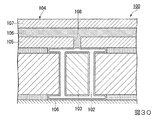
図30に従来の振動式トランスデューサの一例を示す。この図30に示す振動式トランスデューサ100は、測定ダイヤフラムを構成するシリコン基板101を備えている。また、このシリコン基板101の一面側に、真空室102が形成されている。真空室102の内部には振動子103が振動可能に配されている。真空室102の上部には、この真空室102を封止するシェル104が形成されている。
FIG. 30 shows an example of a conventional vibratory transducer. A
シェル104は、真空室102の側から順に、第一ポリシリコン層(第一層)105、第二ポリシリコン層(第二層)106、および第三ポリシリコン層(第三層)107と、を積層してなる。そして、第一ポリシリコン層105には、貫通孔108が形成されている。
The
第一ポリシリコン層105に形成された貫通孔108は、例えば、真空室102を形成する工程において、エッチング液を出し入れする流路となる。そして、この貫通孔108は、エッチング後の廃液を排出する流路として使用された後は、第二ポリシリコン層106の延長部分によって隙間なく塞がれる。
このような構成の振動式トランスデューサ100は、振動子103の共振周波数の変化を検出することによって、振動子に加わる応力(歪)を測定することができる。
The through
The
上述した従来の構成の振動式トランスデューサは、真空室を形成したエッチング廃液を貫通孔から排出する工程や、その後の水洗工程において液体を使用する場合、図31に示すように、これらの液体の微量の液滴Qが振動子103と貫通孔108を含む第一ポリシリコン層105との間に残存していると、液体のメニスカス力によって振動子103が第一ポリシリコン層105の一面側105fに引き寄せられる。その結果、振動子103が第一ポリシリコン層105に付着し、固定化することによって、応力の検出能力を失う虞があった。
また、貫通孔108を隙間なく塞ぐ工程においては、貫通孔108の穴径が大きくなるに従って、真空室102の内部に堆積する第二ポリシリコン層106の厚みが厚くなり、振動子103と、その両側に広がる電極との隙間に堆積して出力信号の大きさにバラツキが生じる。更に、電極どうしが真空室102の内部に堆積した第二ポリシリコン層106によって短絡し、出力が得られなくなる懸念もある。
When the vibration transducer having the conventional configuration described above uses liquids in the step of discharging the etching waste liquid forming the vacuum chamber from the through-hole or in the subsequent water washing step, as shown in FIG. If the liquid droplet Q remains between the
Further, in the step of closing the through
本発明は上記課題に鑑みてなされたものであり、残存する液体や真空室の内部に堆積するポリシリコン層に起因する不具合の発生を回避可能とする構成を備えた振動式トランスデューサおよびその製造方法を提供することを目的としている。 The present invention has been made in view of the above problems, and a vibratory transducer having a configuration capable of avoiding the occurrence of problems caused by the remaining liquid and the polysilicon layer deposited inside the vacuum chamber, and a method of manufacturing the same The purpose is to provide.
上記課題を解決するために、本発明の振動式トランスデューサは、シリコン単結晶の基板に設けられた振動子、該振動子の周辺に隙間が維持されるように前記振動子を囲み、前記基板と共に真空室を区画するシェル、前記振動子を励振させる励振手段、および前記振動子の振動を検出する振動検出手段、を含む振動式トランスデューサであって、前記シェルは、前記真空室の側から順に、貫通孔を有する第一層、該第一層に重ねて配され、前記貫通孔の近傍かつその周囲を覆う第二層、及び、前記第一層と前記第二層とを覆う第三層、から構成され、前記第二層は、前記貫通孔の内部に入り込む突出部を備え、前記シェルは、前記第一層と前記第二層との対向領域において、前記第二層が前記振動子に対向する部位と、前記第二層が前記第三層に接する部位とを連通させる空隙部を有することを特徴とする。 In order to solve the above problems, a vibratory transducer according to the present invention includes a vibrator provided on a silicon single crystal substrate, and surrounds the vibrator so that a gap is maintained around the vibrator, together with the substrate. A vibratory transducer including a shell defining a vacuum chamber, an excitation means for exciting the vibrator, and a vibration detection means for detecting vibration of the vibrator, wherein the shell is sequentially from the vacuum chamber side, A first layer having a through-hole, a second layer that is arranged over the first layer and covers the vicinity of and around the through-hole, and a third layer that covers the first layer and the second layer, The second layer includes a protrusion that enters the inside of the through-hole, and the shell has a region opposite to the first layer and the second layer, and the second layer serves as the vibrator. The opposite part and the second layer are the third It characterized by having a gap portion for communicating the portion contacting the.
前記第一層、前記第二層、および前記第三層は、ポリシリコン、アモルファスシリコン、SiC、SiGe、Geのうち、いずれかよりなることを特徴とする。 The first layer, the second layer, and the third layer are made of any one of polysilicon, amorphous silicon, SiC, SiGe, and Ge.
前記空隙部のギャップを保持するためのスペーサー部が、前記第二層に一体に形成されていることを特徴とする。 A spacer portion for holding the gap of the gap portion is formed integrally with the second layer.
前記突出部の頂面は前記振動子の直上部分にあり、前記第一層の前記真空室側の面よりも前記振動子に近い位置にあることを特徴とする。 The top surface of the projecting portion is located immediately above the vibrator, and is closer to the vibrator than the surface of the first layer on the vacuum chamber side.
前記貫通孔の開口部は、上面より見た時に、前記振動子の長手方向に沿って延びる長方形を成し、前記突出部の外面と前記貫通孔の内面との間で、前記空隙部の一部が筒状に形成されていることを特徴とする。 The opening of the through hole has a rectangular shape that extends along the longitudinal direction of the vibrator when viewed from above, and is formed between the outer surface of the protrusion and the inner surface of the through hole. The portion is formed in a cylindrical shape.
前記貫通孔の開口部は、上面より見た時に、前記振動子の長手方向に沿って配列された円形、または長円形を成し、前記突出部の外面と前記貫通孔の内面との間で、前記空隙部の一部が筒状に形成されていることを特徴とする。 The opening of the through-hole, when viewed from the upper surface, forms a circle or an oval arranged along the longitudinal direction of the vibrator, and between the outer surface of the protrusion and the inner surface of the through-hole. A part of the gap is formed in a cylindrical shape.
また、本発明の振動式トランスデューサの製造方法は、シリコン単結晶の基板に設けられた振動子、該振動子の周辺に隙間が維持されるように前記振動子を囲み、前記基板と共に真空室を区画するシェル、前記振動子を励振させる励振手段、および前記振動子の振動を検出する振動検出手段、を含み、前記シェルは、前記真空室の側から順に、貫通孔を有する第一層、該第一層に重ねて配され、前記貫通孔の近傍かつその周囲を覆う第二層、及び、前記第一層と前記第二層とを覆う第三層、から構成され、前記第二層は、前記貫通孔の内部に入り込む突出部を備え、前記シェルは、前記第一層と前記第二層との対向領域において、前記第二層が前記振動子に対向する部位と、前記第二層が前記第三層に接する部位とを連通させる空隙部を有する振動式トランスデューサの製造方法であって、前記第一層に前記貫通孔を形成する工程と、前記貫通孔とその周囲を覆う犠牲層を形成する工程と、該第一犠牲層に重ねて、前記貫通孔に入り込む前記突出部を有する前記第二層を形成する工程と、前記犠牲層を除去する工程と、を含むことを特徴とする。 The method for manufacturing a vibratory transducer according to the present invention includes a vibrator provided on a silicon single crystal substrate, surrounding the vibrator so that a gap is maintained around the vibrator, and forming a vacuum chamber together with the substrate. A shell for partitioning, an excitation means for exciting the vibrator, and a vibration detection means for detecting the vibration of the vibrator, wherein the shell is, in order from the vacuum chamber side, a first layer having a through-hole, The second layer is arranged to overlap the first layer, and includes a second layer that covers the vicinity of the through hole and the periphery thereof, and a third layer that covers the first layer and the second layer, A protrusion that enters the inside of the through-hole, and the shell has a portion in which the second layer faces the vibrator in a facing region between the first layer and the second layer, and the second layer. Has a void portion that communicates with the portion in contact with the third layer A method of manufacturing a vibratory transducer, the step of forming the through hole in the first layer, the step of forming a sacrificial layer covering the through hole and its surroundings, and overlapping the first sacrificial layer, The method includes a step of forming the second layer having the protruding portion that enters the through hole, and a step of removing the sacrificial layer.
本発明の振動式トランスデューサによれば、第一層と第二層との対向領域に沿って空隙部を形成した。この空隙部のギャップは、第一層と第二層との間に形成される犠牲層の厚みによって正確に制御されるため、再現性良く狭い空隙部を形成することができる。一方、空隙部の隙間を0.1μm程度と狭くすることによって、空隙部を封じ切り真空室を形成する際に、真空室内部に堆積するポリシリコン層をほとんど無くすことができる。
ゆえに、真空室内部に堆積するポリシリコン層に起因する、出力信号の大きさのバラツキや、振動子の共振周波数のバラツキや、電極どうしの短絡による出力不良が回避され、その結果、高精度な応力の検出が可能になる。
According to the vibration type transducer of the present invention, the gap is formed along the facing region between the first layer and the second layer. Since the gap of the gap is accurately controlled by the thickness of the sacrificial layer formed between the first layer and the second layer, a narrow gap can be formed with good reproducibility. On the other hand, by narrowing the gap of the gap portion to about 0.1 μm, the polysilicon layer deposited in the vacuum chamber can be almost eliminated when the gap portion is sealed to form a vacuum chamber.
Therefore, the output signal variation due to the polysilicon layer deposited in the vacuum chamber, the variation in the resonance frequency of the vibrator, and the output failure due to the short circuit between the electrodes can be avoided. Stress can be detected.
また、突出部の頂面を第一層の真空室側の面よりも振動子に近い位置になるように形成することによって、突出部は真空室の内部に突出する形態となる。これにより、振動子と第一層との間にできたエッチング廃液や水洗工程で残留する水滴が除去される過程において、振動子が湾曲して第一層の真空室側の面に吸着される際にも、それぞれの接触する面積を減らし、付着してしまうことを確実に防止できる。 Further, by forming the top surface of the projecting portion so as to be closer to the vibrator than the surface of the first layer on the vacuum chamber side, the projecting portion projects into the inside of the vacuum chamber. As a result, in the process of removing the etching waste liquid formed between the vibrator and the first layer and the water droplets remaining in the water washing step, the vibrator is bent and adsorbed on the vacuum chamber side surface of the first layer. At the same time, it is possible to reduce the area of contact with each other and reliably prevent adhesion.
本発明の振動式トランスデューサの製造方法によれば、振動子と第一層との間に液滴が残って、メニスカス力によって振動子を湾曲させても、付着して固定化することがないように、突出部は真空室の内部に突出する形態となり、第二層の頂面と振動子との接触面積を減らすことによって、エッチング廃液や水洗工程で残留する水滴が除去される過程において、振動子が湾曲して第一層の真空室側の面に吸着される際にも、それぞれの接触面積を減らし、付着してしまうことを確実に防止することができる。
また、第一層と第二層との対向領域に沿って形成した空隙部によって、真空室の内部に堆積するポリシリコン層に起因する、出力信号の大きさのバラツキや、振動子の共振周波数のバラツキや、電極どうしの短絡による出力不良を防止することができる。
According to the method for manufacturing a vibratory transducer of the present invention, liquid droplets remain between the vibrator and the first layer, and even if the vibrator is bent by a meniscus force, it does not adhere and be fixed. In addition, the protrusions protrude into the interior of the vacuum chamber, and vibration is reduced in the process of removing etching waste liquid and water droplets remaining in the water washing process by reducing the contact area between the top surface of the second layer and the vibrator. Even when the child is bent and adsorbed to the surface of the first layer on the vacuum chamber side, the contact area can be reduced and it can be reliably prevented from adhering.
In addition, the gap formed along the opposing area between the first and second layers causes variations in the magnitude of the output signal due to the polysilicon layer deposited inside the vacuum chamber, and the resonance frequency of the vibrator. And output failures due to short-circuiting between electrodes can be prevented.
以下、図面を参照して、本発明の振動式トランスデューサおよびその製造方法について説明する。なお、本実施形態は、発明の趣旨をより良く理解させるために具体的に説明するものであり、特に指定のない限り、本発明を限定するものではない。また、以下の説明で用いる図面は、本発明の特徴をわかりやすくするために、便宜上、要部となる部分を拡大して示している場合があり、各構成要素の寸法比率などが実際と同じであるとは限らない。 Hereinafter, with reference to the drawings, a vibration type transducer and a manufacturing method thereof according to the present invention will be described. The present embodiment is specifically described for better understanding of the gist of the invention, and does not limit the invention unless otherwise specified. In addition, in the drawings used in the following description, in order to make the features of the present invention easier to understand, there is a case where a main part is shown in an enlarged manner for convenience, and the dimensional ratio of each component is the same as the actual one. Not necessarily.
(振動式トランスデューサ:第一実施形態)
図1は、本発明の振動式トランスデューサの厚み方向に沿った断面図である。また、図2は、本発明の振動式トランスデューサのシェルを取り除いて上から見た時の平面図である。
本発明の一実施形態である振動式トランスデューサ10は、シリコン単結晶からなる基板11に、周辺に隙間が維持されるように形成された振動子12を備えている。また、この基板11と共に振動子12を囲んで真空室21を区画するシェル14を備えている。
(Vibration transducer: First embodiment)
FIG. 1 is a cross-sectional view along the thickness direction of the vibration type transducer of the present invention. FIG. 2 is a plan view of the vibratory transducer according to the present invention as viewed from above with the shell removed.
A
基板11の一面11aには、所定の形状に区画された真空室21が配され、この真空室21の内部に、振動子12、第一電極15、第二電極16、および第三電極17が配されている。また、真空室21の外側には、この真空室21の側壁を構成するエピタキシャル層18が広がっている。このエピタキシャル層18と、振動子12、第一電極15、第二電極16、および第三電極17とは、同一の材料、例えば、ボロンをドープさせた低抵抗のP型半導体から構成される。
A
振動子12は、第一電極15と一体の部材を成し、第一電極15に対して電気的に接続されている。振動式トランスデューサ10をシェル14側から平面視した時に、振動子12は、狭い幅で細長く延び、厚み方向に広がる略板状を成している。振動子12の厚み方向の長さは、基板11の面広がり方向に沿った幅よりも長くなるように形成されている。また、こうした略板状の振動子12は、基板11に対して所定の引張応力が付与されている。そして、この略板状の振動子12の一端側に、第一電極15が一体に接続されている。
The
第二電極16および第三電極17は、振動子12の長手方向の両側から挟むように、かつ振動子12に対して所定のギャップを保って配置された略直方体形状の部材である。
これら第一電極15、第二電極16、および第三電極17には、それぞれ、外部の電気回路と接続される接片15a,16a,17aが形成されている。これら接片15a,16a,17aは、例えば金属から形成されていればよい。
The
The
第一電極15、第二電極16、および第三電極17と、シェル14との間のうち、真空室21を除いた部分には、絶縁層22が形成されている。また、第一電極15、第二電極16、および第三電極17と、基板11の一面11aとの間のうち、真空室21を除いた部分には、絶縁層23が形成されている。この絶縁層23は、振動式トランスデューサの製造工程において、基板11としてSOI基板を用いることによって形成される。なお、振動式トランスデューサの製造方法は、後ほど詳述する。
An insulating
真空室21は、内部が所定の真空度に保たれている。振動子12、第一電極15、第二電極16、および第三電極17は、真空室21を区画している部材、即ち基板11、エピタキシャル層18、およびシェル14に対して、所定の間隔を保って配置されている。
The inside of the
図3は、図1における振動子とシェルとの対向部分を示す要部拡大断面図である。
シェル14は、真空室21の側から順に、第一ポリシリコン層(第一層)26と、この第一ポリシリコン層26に重ねて配される第二ポリシリコン層(第二層)27と、第一ポリシリコン層26及び第二ポリシリコン層27を覆う第三ポリシリコン層(第三層)28と、から構成されている。
FIG. 3 is an enlarged cross-sectional view of a main part showing a facing portion between the vibrator and the shell in FIG.
The
なお、シェル14を構成するこれら3つの層(第一層、第二層、第三層)は、本実施形態ではポリシリコンによって形成しており、それぞれ第一ポリシリコン層26、第二ポリシリコン層27、第三ポリシリコン層28と称している。しかしながら、これらシェル14を構成するこれら3つの層(第一層、第二層、第三層)は、ポリシリコンに限定されるものではなく、例えば、アモルファスシリコン、SiC、SiGe、Geなどを用いることもできる。
Note that these three layers (first layer, second layer, and third layer) constituting the
第一ポリシリコン層(第一層)26は、真空室21、および絶縁層22に接するように形成されている。この第一ポリシリコン層26が真空室21に重なる部分には、貫通孔25が形成されている。貫通孔25は、第一ポリシリコン層26の厚み方向に沿って延設されている。なお、以下の説明において、貫通孔25における真空室21側の開口部を第一開口部25a、第二ポリシリコン層27側の開口部を第二開口部25bと称することがある。
The first polysilicon layer (first layer) 26 is formed in contact with the
図4に示すように、本実施形態においては、貫通孔25の第一開口部25aや第二開口部25bは、第三ポリシリコン層側から見た時に、振動子12の長手方向に沿って、所定の幅で延びる長方形を成している。即ち、貫通孔25は、振動子12の長手方向に沿って延びる細長い直方体の空間を構成している。
As shown in FIG. 4, in the present embodiment, the
第二ポリシリコン層(第二層)27は、貫通孔25の第二開口部25bの近傍かつその周囲を覆うように配されている。具体的には、貫通孔25の第二開口部25b側を覆うとともに、第二開口部25bの周囲を貫通孔25の長手方向に沿って所定の幅で延びるように形成されている。
The second polysilicon layer (second layer) 27 is disposed so as to cover the vicinity of the
また、第二ポリシリコン層27の貫通孔25側には、突出部29が一体に形成されている。この突出部29は、第二開口部25b側から貫通孔25の内部に入り込むように形成されている。そして、突出部29の頂面29aは、第一ポリシリコン層26の真空室21側の面26aよりも振動子12から遠ざかった位置になるように形成されている。
Further, a protruding
第三ポリシリコン層(第三層)28は、第一ポリシリコン層26と第二ポリシリコン層27とを覆うように形成されている。具体的には、第二ポリシリコン層27の形成領域においては、この第二ポリシリコン層27に接するように形成され、第二ポリシリコン層27の形成領域よりも外側領域においては、第一ポリシリコン層26と直接接するように形成されている。
The third polysilicon layer (third layer) 28 is formed so as to cover the
このような積層構造をもつシェル14には、第一ポリシリコン層26と第二ポリシリコン層27との対向領域において、第二ポリシリコン層27が振動子12に対向する部位E1と、第二ポリシリコン層27が第三ポリシリコン層28に接する部位E2とを連通させる空隙部31が形成されている。
In the
具体的には、空隙部31の形状は、図1に示す断面図においては、第一ポリシリコン層26と第二ポリシリコン層27との対向領域に沿った略L字型を成す幅の狭い空間である。こうした空隙部31の一方の開口端を成す部位E1は、貫通孔25の第一開口部25aにおける側壁と、第二ポリシリコン層27の突出部29との隙間部分である。また、空隙部31の他方の開口端を成す部位E2は、第二ポリシリコン層27の厚み方向に沿った周壁と第一ポリシリコン層26との隙間部分である。
Specifically, in the cross-sectional view shown in FIG. 1, the shape of the
このような空隙部31のギャップ、即ち、対向する第一ポリシリコン層26と第二ポリシリコン層27との隙間の幅は、例えば、真空室21を形成する際に用いるエッチング液が流入、流出可能な程度であればよい。
The gap between the
第二ポリシリコン層27が空隙部31に面する部分には、この空隙部31のギャップを保持するためのスペーサー部32が、第二ポリシリコン層27と一体に形成されている。スペーサー部32は、第二ポリシリコン層27から突出し、その頂面が第一ポリシリコン層26に接することによって、空隙部31のギャップが応力等の印加によって狭められないように、空隙部31を所定の幅に維持する。こうしたスペーサー部32の高さは、空隙部31のギャップと同じになるように形成されていればよい。
In the portion where the
図4に示すように、スペーサー部32は、空隙部31の形成領域において、貫通孔25の長手方向に沿った両側に、間欠的に複数形成されていればよい。空隙部31(図3参照)を流れる液体、例えばエッチング液は、こうしたスペーサー部32どうしの間を通る。このため、スペーサー部32は、液体の流通を妨げず、かつ空隙部31のギャップを維持できる程度の密度で形成されていればよい。個々のスペーサー部32の形状は、本実施形態では長楕円柱状に形成されている。
As shown in FIG. 4, the
図5は、振動式トランスデューサの回路の概要を示す回路図である。
振動式トランスデューサ10は、振動子12を励振させる励振手段41と、振動子12の振動を検出する振動検出手段42とを有している。励振手段41は、前述した第一電極15、第二電極16、および第三電極17とから構成されている。
振動検出手段42は、駆動電源43、バイアス電源44、抵抗R1,R2,R3、および演算増幅器(オペアンプ)OP1,OP2などから構成されている。
FIG. 5 is a circuit diagram showing an outline of the circuit of the vibration transducer.
The
The vibration detection means 42 includes a
駆動電源43からは、所定の駆動電圧Viの交流電圧が印加される。また、バイアス電源44からは、所定のバイアス電圧Vbの直流電圧が印加される。第一電極15には、バイアス電源44から定電圧のバイアス電圧Vbが加えられる。また、第二電極16には、駆動電源43から交流の駆動電圧Viが加えられる。また、第三電極17から振動子12の振動周波数に応じた検出信号が取り出される。
An AC voltage having a predetermined drive voltage Vi is applied from the
以上のような構成の振動式トランスデューサの動作を説明する。
第一電極15に定電圧のバイアス電圧Vbが印加され、また、第二電極16に交流の駆動電圧Viが印加されると、第一電極15に繋がる振動子12と第二電極16との間に静電吸引力が発生し、振動子12が一定の振動周波数で振動(共振)する。
The operation of the vibration type transducer having the above configuration will be described.
When a constant bias voltage Vb is applied to the
一方、第一電極15に繋がる振動子12と、第三電極17との間には、第一電極15に印加されたバイアス電圧Vbによって電荷が貯められ、振動子12が振動して振動子12と第三電極17との間の静電容量が変化すると、それに対応した交流電流である検出信号が発生する。こうした検出信号を演算増幅器OP1,OP2で増幅し、電圧変化としてカウンターで読み込むことによって、振動子12の振動周波数が測定される。
On the other hand, a charge is stored between the
そして、振動子12に応力が加わって歪が生じると、この歪の量に応じて振動子12の振動周波数が変動する。こうした振動子12の振動周波数の変動量と、振動子12の歪の量との関係を参照することによって、振動子12の歪の量、即ち、振動子12に加わる応力を測定することができる。
When stress is applied to the
このような構成では、励起電極となる第二電極16と、検出電極となる第三電極17とを離すことができるため、第二電極16と第三電極17との間の寄生容量が減少する。その結果、駆動電圧Viが検出回路側に回り込むクロストークが抑えられ、SN比を向上させることができる。
In such a configuration, since the
(振動式トランスデューサの製造方法:第一実施形態)
以上のような構成の振動式トランスデューサの製造方法、および振動式トランスデューサの作用を説明する。
(Manufacturing method of vibratory transducer: first embodiment)
A method of manufacturing the vibration type transducer having the above configuration and the operation of the vibration type transducer will be described.
図6〜図15は、本発明の振動式トランスデューサの製造方法を段階的に説明した要部拡大断面図である。なお、これら図6〜図15は、図2におけるA−A線に沿った部分の断面を示している。
まず、図6に示すように、Siからなる基板11に酸化層52、表面シリコン層53が形成されたSOI基板51を準備する。例えば、SOI基板51は、酸化層52の厚みが2μm程度、活性層である表面シリコン層53の厚みが1μm程度のものを用いればよい。
FIGS. 6 to 15 are enlarged cross-sectional views of the main part for explaining the manufacturing method of the vibratory transducer of the present invention step by step. 6 to 15 show a cross section of a portion along the line AA in FIG.
First, as shown in FIG. 6, an
次に、図7に示すように、この活性層である表面シリコン層53に、高濃度にホウ素が含まれたエピタキシャルシリコン層54をエピタキシャル成長によって形成する。こうした高濃度にホウ素がが含まれたエピタキシャルシリコン層54は、電気抵抗が小さく導体として作用し、後工程において振動子12や第一電極15、第二電極16、および第三電極17(図2参照)が形成される。
Next, as shown in FIG. 7, an
また、高濃度にホウ素が含まれたエピタキシャルシリコン層54は、基板11に比べて引っ張り応力を残留しているため、後工程で形成する振動子12に張力を発生させる。振動子12は張力領域で応力が印加された場合、応力に対して周波数の2乗が比例するように変化し、きわめて直線性の良い特性が得られる。一方で、圧縮応力領域での動作は、非常に非線形な特性となるため、振動式トランスデューサ10の動作は、引っ張り応力領域で行われるようにする。
Further, the
高濃度にホウ素を含んだエピタキシャルシリコン層54の成長条件としては、成長温度1030℃、H2ガス中で、Si原料ガスとしてジクロロシラン(SiH2Cl2)、不純物であるボロンの原料ガスとしてジボラン(B2H6)を用い、一定時間エピタキシャル成長を行うことによって高濃度にホウ素が含まれたエピタキシャルシリコン層54を例えば9μm程度成長させ、活性層である表面シリコン層53との合計厚みが10μm程度となるようにする。
As growth conditions for the
次に、図8に示すように、高濃度にホウ素が含まれたエピタキシャルシリコン層54のパターニングを行い、エピタキシャルシリコン層54の一部に振動子12、第一電極15(図2参照)、第二電極16、および第三電極17の輪郭となるトレンチTを形成する。エピタキシャルシリコン層54のパターニングは、例えば、エピタキシャルシリコン層54にレジスト材を塗布し、ステッパ装置を用いてパターニングを行う。
Next, as shown in FIG. 8, the
ステッパ装置は、例えば、0.3μm程度の分解能を持ち、サブミクロンのラインおよびスペースの露光が可能である。こうしたステッパ装置によって、振動子12、第一電極15、第二電極16、および第三電極17の輪郭パターンを形成する。
The stepper apparatus has, for example, a resolution of about 0.3 μm and can expose submicron lines and spaces. With such a stepper device, contour patterns of the
そして、ステッパ装置によって形成したレジストを層をマスクとして、エピタキシャルシリコン層54をエッチングし、振動子12、第一電極15、第二電極16、および第三電極17の輪郭を象ったトレンチTを形成する。エピタキシャルシリコン層54のエッチングは、例えば、ドライエッチングによって行う。また、ドライエッチングはSOI基板51を構成する酸化層52に突き当たり、振動子12と第一電極15、第二電極16、および第三電極17とが電気的に分離されるまで行う。
Then, using the resist formed by the stepper device as a mask, the
こうしたドライエッチングによるトレンチの形成時に、例えば、シリコンのエッチング工程とCFポリマーのデポジション工程を繰り返し行うことによって、エッチングされるトレンチの側壁面に襞状の凸凹部を形成することも好ましい。例えば、エッチング時間とデポジション時間を調整することによって、0.1μm程度またはそれ以上の凸凹で、ピッチが0.1μm〜1μm程度の水平方向の縞を形成することができる。 At the time of forming a trench by such dry etching, for example, it is also preferable to form a ridge-like convex / concave portion on the side wall surface of the trench to be etched by repeatedly performing a silicon etching process and a CF polymer deposition process. For example, by adjusting the etching time and the deposition time, it is possible to form horizontal stripes having a pitch of about 0.1 μm to 1 μm with unevenness of about 0.1 μm or more.
次に、図9に示すように、エピタキシャルシリコン層54において振動子12、第一電極15、第二電極16、および第三電極17の輪郭を象ったトレンチTを埋め、さらにエピタキシャルシリコン層54の一面に所定の厚みで堆積するように、絶縁層56を形成する。絶縁層56は、例えば、酸化ケイ素から構成されている。トレンチTを埋める絶縁層56の形成には、例えば、テトラエトキシシラン(TEOS)を用いたLP−CVD酸化膜やプラズマCVD酸化膜によってトレンチTの開口部分を封鎖する。
Next, as shown in FIG. 9, the trench T that represents the outline of the
LP−CVD酸化膜は、例えば、温度700℃、圧力50Paの真空中で、TEOSタンクをバブリングして含んだ窒素ガスおよび、酸素ガスを導入して、TEOSを熱分解させることによって、トレンチTを埋める酸化ケイ素を形成する。 The LP-CVD oxide film, for example, introduces a trench T by thermally decomposing TEOS by introducing nitrogen gas and oxygen gas contained by bubbling the TEOS tank in a vacuum of a temperature of 700 ° C. and a pressure of 50 Pa. Form silicon oxide to fill.
プラズマCVD酸化膜は、真空中でTEOSと酸素ガスとを導入してプラズマを発生させ、400℃に加熱されたステージ上に置かれた基板上で、トレンチTを埋める酸化ケイ素を形成する。なお、プラズマCVD装置はステップカバレッジがよくないため、絶縁層56がトレンチTの最深部まで稠密に成膜されにくく、一部に空間(ボイド)Vが形成される。
The plasma CVD oxide film generates plasma by introducing TEOS and oxygen gas in a vacuum, and forms silicon oxide filling the trench T on a substrate placed on a stage heated to 400 ° C. Since the plasma CVD apparatus does not have good step coverage, the insulating
次に、図10に示すように、エピタキシャルシリコン層54の一面を覆う絶縁層56に重ねて、例えば数μmの厚みの第一ポリシリコン層(第一層)26を形成する。この第一ポリシリコン層26は、後工程で形成される真空室21を区画するシェル14の一部を構成している。
Next, as shown in FIG. 10, a first polysilicon layer (first layer) 26 having a thickness of, for example, several μm is formed on the insulating
次に、図11に示すように、第一ポリシリコン層26の一部に貫通孔25を形成する。貫通孔25は、例えば、振動子12と重なる位置に形成される。貫通孔25の形成は、例えば、第一ポリシリコン層26に貫通孔25の輪郭を象ったレジスト層を形成した後、ドライエッチングによって第一ポリシリコン層26を厚み方向に貫通する貫通孔25を形成すればよい。貫通孔25は、例えば、振動子12の長手方向に沿って延びる細長い直方体の空間を成すように形成される(図4参照)。
Next, as shown in FIG. 11, a through
次に、図12に示すように、第一ポリシリコン層26の一面側、および貫通孔25の内面を覆う酸化被膜(犠牲層)57を形成する。こうした酸化被膜57の一部、具体的には、貫通孔25の第二開口部25bの周囲には、後工程で形成する第二ポリシリコン層27のスペーサー部32(図3参照)の外形形状を象った窪み58が形成される。
Next, as shown in FIG. 12, an oxide film (sacrificial layer) 57 that covers one surface side of the
こうした窪み58を有する酸化被膜57は、例えば、LP−CVD装置を用いて、厚みが100nm程度の酸化ケイ素膜を、貫通孔25とその周囲のみパターニングし、それ以外の領域をバッファードフッ酸にて除去すればよい。
The
次に、図13に示すように、貫通孔25の近傍かつその周囲を覆うように、第二ポリシリコン層(第二層)27を形成する。第二ポリシリコン層27の第一ポリシリコン層26側には、酸化被膜57で覆われた貫通孔25の内部に入り込む突出部29と、酸化被膜57に形成された窪み58を象ったスペーサー部32とが、それぞれ一体に形成される。
Next, as shown in FIG. 13, a second polysilicon layer (second layer) 27 is formed so as to cover the vicinity of the through
次に、図14に示すように、希HF溶液を用いて、酸化被膜(犠牲層)57(図13参照)の全体、および振動子12の周囲の絶縁層56(図13参照)、酸化層52(図13参照)をエッチングして除去する(真空室を形成したエッチング液を、空隙部から外部に排出させる工程)。これによって、振動子12の周囲には真空室21が形成され、振動子12は、この真空室21によって周辺に隙間が維持された形態にされる。
Next, as shown in FIG. 14, the whole oxide film (sacrificial layer) 57 (see FIG. 13), the insulating layer 56 (see FIG. 13) around the
一方、第一ポリシリコン層26と第二ポリシリコン層27との間に形成されていた酸化被膜57が除去されることによって、第一ポリシリコン層26と第二ポリシリコン層27との対向領域において、第二ポリシリコン層27が振動子12に対向する部位E1と、第二ポリシリコン層27が第三ポリシリコン層28に接する部位E2とを連通させる空隙部31が形成される。このような空隙部31を介して、振動子12の周囲の絶縁層56や酸化層52まで希HF溶液が到達する。
On the other hand, by removing the
振動子12の周囲の絶縁層56、酸化層52をエッチングして真空室21を形成した希HF溶液の廃液は、真空室21内から空隙部31を介して外部に排出される。この時、廃液がほぼ排出されて、残りの少量の廃液が振動子12と第二ポリシリコン層27の突出部29の頂面29aとの間に位置する時に、廃液にメニスカス力が働くことがある。廃液にメニスカス力が働くと、振動可能な振動子12が第二ポリシリコン層27の突出部29側に引き寄せられるように湾曲し、振動子12が変形する懸念がある。
The waste solution of the diluted HF solution formed by etching the insulating
しかしながら、第一ポリシリコン層26と第二ポリシリコン層27との対向領域に、幅の狭い空隙部31が形成されているので、貫通孔25の第一開口部25a付近に残っている少量の廃液は、空隙部31で生じる毛細管現象によって速やかに吸い上げられる。これより、貫通孔25の第一開口部25a付近に液滴状の廃液のメニスカス力によって振動子12が変形し、付着して固定化することが無いように、突出部29は真空室21の内部に突出する形態となり、第二ポリシリコン層27の頂面29aと振動子12との接触面積を減らすことによって、エッチング廃液や水洗工程で残留する水滴が除去される過程において、振動子12が湾曲して第一ポリシリコン層26の真空室21側の面に吸着される際にも、付着してしまうことを確実に防止することができる。
また、第一ポリシリコン層26と第二ポリシリコン層27との対向領域に沿って形成した空隙部31によって、真空室21の内部に堆積するポリシリコン層に起因する、出力信号の大きさのバラツキや、振動子12の共振周波数のバラツキや、電極どうしの短絡による出力不良を防止することができる。
However, since the
Further, the size of the output signal caused by the polysilicon layer deposited inside the
この後、図15に示すように、第一ポリシリコン層26と第二ポリシリコン層27とを覆うように、第三ポリシリコン層(第三層)28を形成して真空封止を行う。第三ポリシリコン層28による真空封止は、製膜された第三ポリシリコン層28が引っ張り歪となるか、あるいは残留圧縮歪がほとんどなくなる条件で行う。例えば、減圧エピタキシャル装置を用いて、900℃以下の温度で行えばよい。原料ガスには、SiH4または、SiH4と水素の混合物を用いればよい。
Thereafter, as shown in FIG. 15, a third polysilicon layer (third layer) 28 is formed so as to cover the
この後、図1、図2に示す接片15a,16a,17c(図1参照)を露出させる穴を、第一ポリシリコン層26と第三ポリシリコン層28とが接した部分に形成して、振動式トランスデューサ10のセンサー部分を得ることができる。
Thereafter, holes for exposing the
以上のように、本発明の振動式トランスデューサや、その製造方法によれば、エッチング廃液や水洗工程で残留する水滴が除去される過程において、振動子12と第一ポリシリコン層26との間に残った液滴のメニスカス力によって振動子12を湾曲させて第一ポリシリコン層26の真空室21側の面に吸着される際にも、付着して固定化することがないように、突出部29が真空室21の内部に突出する形態となった第二ポリシリコン層27の突出部29の頂面29aと振動子12との接触面積を少なくし、付着によって固着して変形することを確実に防止できる。
また、第一ポリシリコン層26と第二ポリシリコン層27との対向領域に沿って形成した狭い空隙部31によって、真空室21の内部に堆積するポリシリコン層をほとんど無くすことができるため、出力信号の大きさのバラツキや、振動子12の共振周波数のバラツキや、電極どうしの短絡による出力不良を防止することができる。
As described above, according to the vibratory transducer of the present invention and the manufacturing method thereof, in the process of removing etching waste liquid and water droplets remaining in the water washing process, the
Further, since the
以下、振動式トランスデューサの別な実施形態を列記する。なお、それぞれの実施形態において、第一実施形態と同一の構成には同一の番号を付し、その説明を省略する。 Hereinafter, another embodiment of the vibration type transducer will be listed. In each embodiment, the same components as those in the first embodiment are denoted by the same reference numerals, and the description thereof is omitted.
(振動式トランスデューサ:第二実施形態)
第一実施形態においては、第一ポリシリコン層26に形成される貫通孔25の形状は、振動子12の長手方向に沿って、所定の幅で延びる一連の細長い直方体の空間を成している。しかし、貫通孔の形状やこれを覆う第二ポリシリコン層の形状はこれらに限定されるものではない。
(Vibration transducer: second embodiment)
In the first embodiment, the shape of the through-
図16に示す振動式トランスデューサ60では、第一ポリシリコン層(第一層)26に円筒形の貫通孔61,61…を振動子12の長手方向に沿って、複数配列している。即ち、貫通孔61の開口部は、上面より見た時に、振動子12の長手方向に沿って複数配列された円形を成している。また、第二ポリシリコン層(第二層)27には、これら貫通孔61,61…のそれぞれの内部に入り込む複数の突出部62,62…が一体に形成されている。
こうした構成によって、突出部62の外面と貫通孔61の内面との間で、空隙部31の一部が円筒状になるように形成される。
In the
With such a configuration, a part of the
そして、第一ポリシリコン層26における個々の貫通孔61の第二開口部61bの周囲に接するように、第二ポリシリコン層27にスペーサ部材63が一体に形成されている。例えば、図16に示す振動式トランスデューサ60では、スペーサ部材63は、個々の貫通孔61の第二開口部61bを取り巻く位置で接するように、複数形成されている。
A
(振動式トランスデューサ:第三実施形態)
図17に示す振動式トランスデューサ65では、第一ポリシリコン層(第一層)26に直方体の貫通孔66,66…を振動子12の長手方向に沿って、複数配列している。即ち、貫通孔65の開口部は、上面より見た時に、振動子12の長手方向に沿って延びる長方形を成している。また、第二ポリシリコン層(第二層)27には、これら貫通孔66,66…のそれぞれの内部に入り込む複数の円筒形の突出部67,67…が一体に形成されている。
こうした構成によって、突出部67の外面と貫通孔66の内面との間で、空隙部31の一部が四角筒状になるように形成される。
(Vibration transducer: third embodiment)
17, a plurality of rectangular parallelepiped through
With such a configuration, a part of the
そして、第一ポリシリコン層26における個々の貫通孔66の第二開口部66bの周囲に接するように、第二ポリシリコン層27にスペーサ部材68が一体に形成されている。例えば、図17に示す振動式トランスデューサ65では、スペーサ部材68は、個々の貫通孔66の第二開口部66bの長手方向に沿った両側で接するように、複数形成されている。
A
なお、上述した実施形態以外にも、貫通孔66の開口部の形状としては、長円形、楕円形、三角形、あるいは多角形、不定形など、各種形状に形成することができ、限定されるものではない。
In addition to the above-described embodiment, the shape of the opening of the through
また、第一ポリシリコン層26と第二ポリシリコン層27との対向領域に形成される空隙部31(図3参照)のギャップを維持するスペーサ部材は、上述した第一実施形態や第二実施形態のような形状以外にも、例えば、第一ポリシリコン層26と第二ポリシリコン層27との対向領域における、第一ポリシリコン層26または第二ポリシリコン層27のいずれか一方、または両方を不規則な凹凸形状にするなど空隙部を形成し、流体の通過を許容するような構成であってもよい。この場合、第一ポリシリコン層26や第二ポリシリコン層27の一部に粗面を形成することによって実現できる。
The spacer member for maintaining the gap of the gap 31 (see FIG. 3) formed in the opposed region between the
(振動式トランスデューサ:第四実施形態)
図18は、振動式トランスデューサの第四実施形態を示す要部拡大断面図である。
本実施形態の振動式トランスデューサ70は、シェル14を構成する第一ポリシリコン層26(第一層)に、真空室21と連通する貫通孔25が形成されている。真空室21には、振動子12が振動可能に形成されている。そして、第二ポリシリコン層(第二層)27には、貫通孔25の内側面との間で空隙部31を形成しつつ貫通孔25に入り込む突出部71が一体に形成されている。
(Vibration transducer: Fourth embodiment)
FIG. 18 is an enlarged cross-sectional view of a main part showing a fourth embodiment of the vibration type transducer.
In the
そして、この突出部71の頂面71aは、振動子12の直上部分にあり、かつ第一ポリシリコン層26の真空室21側の面26fよりも振動子12に近い位置になるように形成されている。即ち、突出部71は、第二ポリシリコン層27から延び、貫通孔25の第二開口部25b側から第一開口部25a側までを貫通し、更に真空室21内に突出した形状となっている。
The
第二ポリシリコン層27の突出部71をこのような形状にすることによって、振動子12が第一ポリシリコン層26へ付着することをより一層確実に防止することができる。例えば、振動式トランスデューサ70の真空室21を形成する工程において、エッチング液の廃液を空隙部31から流出させる際に、振動子12と第一ポリシリコン層26の第一開口部25との間付近に残った廃液のメニスカス力によって、振動子12が第一ポリシリコン層26側に大きく湾曲しようとしても、真空室21内に張り出した突出部71の頂面71aに当接する。
By forming the protruding
これによって、振動子12が第一ポリシリコン層26の真空室21側の面26fまで大きく湾曲して付着してしまうことを確実に防止することが可能になる。特に、振動子12の幅よりも、突出部71の頂面71aの幅が狭くなるように形成することによって、振動子12が湾曲して突出部71の頂面71aに接触したとしても、その接触面積を小さくして、振動子12が突出部71に吸着されてしまうことを防止できる。
As a result, it is possible to reliably prevent the
(振動式トランスデューサの製造方法:第二実施形態)
図19〜図23は、第二実施形態の振動式トランスデューサの製造方法を段階的に示した要部拡大断面図である。
図19は、第一実施形態の振動式トランスデューサの製造方法における図10に相当する工程である。図19に示すように、エピタキシャルシリコン層54の一面を覆う絶縁層56に重ねて、例えば数μmの厚みの第一ポリシリコン層(第一層)81を形成する。この時、例えば、エピタキシャル装置を用いて第一ポリシリコン層81を形成し、結晶粒径に応じて決定される微細な凹凸82を表面に形成する。
(Manufacturing method of vibratory transducer: second embodiment)
FIG. 19 to FIG. 23 are enlarged cross-sectional views of the main part showing the manufacturing method of the vibratory transducer according to the second embodiment step by step.
FIG. 19 is a process corresponding to FIG. 10 in the method for manufacturing the vibration type transducer of the first embodiment. As shown in FIG. 19, a first polysilicon layer (first layer) 81 having a thickness of, for example, several μm is formed on the insulating
次に、図20に示すように、第一ポリシリコン層81の一部に貫通孔83を形成する。貫通孔83は、例えば、振動子12と重なる位置に形成される。貫通孔83の形成は、例えば、第一ポリシリコン層81に貫通孔83の開口部の輪郭を象ったレジスト層を形成した後、ドライエッチングによって第一ポリシリコン層81を厚み方向に貫通し、絶縁層56の途中まで達する貫通孔83を形成すればよい。この時、貫通孔83の絶縁層56側の底面にも、表面に微細な凹凸84を形成する。
Next, as shown in FIG. 20, a through
なお、これら図19に示す工程と、図20に示す工程とは、例えば、ポリシリコンと絶縁層(酸化シリコン)とのエッチング比が低い、材質選択性ドライエッチングによって、一連のエッチング工程として行うことができる。 The steps shown in FIG. 19 and the step shown in FIG. 20 are performed as a series of etching steps by, for example, material-selective dry etching having a low etching ratio between polysilicon and an insulating layer (silicon oxide). Can do.
次に、図21に示すように、第一ポリシリコン層81に形成した微細な凹凸82と、貫通孔83の内周面、および絶縁層56側の底面の微細な凹凸84を覆う酸化被膜86を形成する。
Next, as shown in FIG. 21, the
次に、図22に示すように、貫通孔83の近傍かつその周囲を覆うように、第二ポリシリコン層(第二層)87を形成する。第二ポリシリコン層87の第一ポリシリコン層81側には、酸化被膜86で覆われた貫通孔83の内部に入り込み、絶縁層56の途中まで達する突出部88が形成される。こうした突出部88の頂面88aには、貫通孔83の絶縁層56側の底面に形成された微細な凹凸84を象った凹凸89が形成される。
Next, as shown in FIG. 22, a second polysilicon layer (second layer) 87 is formed so as to cover the vicinity of the through
次に、図23に示すように、希HF溶液を用いて、酸化被膜86の全体、および振動子12の周囲の絶縁層56、酸化層52をエッチングして除去する。これによって、振動子12の周囲には真空室21が形成され、振動子12は、この真空室21によって周辺に隙間が維持された形態にされる。
Next, as shown in FIG. 23, the
一方、第一ポリシリコン層81と第二ポリシリコン層87との間に形成されていた酸化被膜86が除去されることによって、第一ポリシリコン層81と第二ポリシリコン層87との対向領域において、第二ポリシリコン層87が振動子12に対向する部位E1と、第二ポリシリコン層87が第三ポリシリコン層28(図1参照)に接する部位E2とを連通させる空隙部31が形成される。このような空隙部31を介して、真空室21を形成するための希HF溶液が流入、流出される。
On the other hand, by removing the
このような構成の振動式トランスデューサの製造方法によれば、少量の希HF溶液の廃液が振動子12と貫通孔83の第一開口部83aとの間付近に残留し、廃液のメニスカス力によって振動子12が第一ポリシリコン層81側に大きく湾曲しようとしても、真空室21内に張り出した突出部88の頂面88aに当接する。これによって、振動子12が第一ポリシリコン層81の真空室21側の面81fまで大きく湾曲して変形してしまうことを確実に防止することが可能になる。
According to the manufacturing method of the vibration type transducer having such a configuration, a small amount of dilute HF solution waste liquid remains in the vicinity between the
しかも、この第二実施形態の製造方法によれば、突出部88の頂面88aには微細な凹凸89が形成されているので、突出部88に対する振動子12の接触面積が極めて小さくなり、振動子12が突出部88の頂面88aに吸着されてしまうことがない。よって、振動子12の変形を確実に防止することができる。
Moreover, according to the manufacturing method of the second embodiment, since the
(振動式トランスデューサの製造方法:第三実施形態)
図24〜図29は、第三実施形態の振動式トランスデューサの製造方法を段階的に示した要部拡大断面図である。
図24は、第一実施形態の振動式トランスデューサの製造方法における図10に相当する工程である。図24に示すように、エピタキシャルシリコン層54の一面を覆う絶縁層56に重ねて、例えば数μmの厚みの第一ポリシリコン層(第一層)91を形成する。この時、第一ポリシリコン層91の一面側にドライエッチングを行い、表面に微細な凹凸92を形成する。
(Manufacturing method of vibration transducer: third embodiment)
FIGS. 24 to 29 are enlarged cross-sectional views of the main part showing the manufacturing method of the vibratory transducer according to the third embodiment step by step.
FIG. 24 is a process corresponding to FIG. 10 in the method for manufacturing the vibration type transducer of the first embodiment. As shown in FIG. 24, a first polysilicon layer (first layer) 91 having a thickness of, for example, several μm is formed on the insulating
次に、図25に示すように、第一ポリシリコン層91を貫通する貫通孔93を形成する。貫通孔93は、例えば、振動子12と重なる位置に形成される。貫通孔93の形成は、例えば、第一ポリシリコン層91に貫通孔93の開口部の輪郭を象ったレジスト層を形成した後、ドライエッチングによって第一ポリシリコン層91を厚み方向に貫通し、絶縁層56の途中まで達する貫通孔93を形成すればよい。
Next, as shown in FIG. 25, a through
更に、図26に示すように、貫通孔93から絶縁層56を等方エッチングすることによって、第一ポリシリコン層91の貫通孔93の幅よりも広い直径の断面半円形の底面99をもつ穴を絶縁層56に形成する。このような形状となるエッチングを行うために、例えば、エッチングレートがポリシリコンよりも酸化シリコンのほうが大きく、かつ、酸化シリコンを等方エッチング可能なエッチング液を用いる。
Further, as shown in FIG. 26, the insulating
次に、図27に示すように、第一ポリシリコン層91に形成した微細な凹凸92と、貫通孔93の内周面、および絶縁層56側の断面半円形の底面99を覆う酸化被膜96を形成する。
Next, as shown in FIG. 27, an
次に、図28に示すように、貫通孔93の近傍かつその周囲を覆うように、第二ポリシリコン層(第一層)97を形成する。第二ポリシリコン層97の第一ポリシリコン層91側には、酸化被膜96で覆われた貫通孔93の内部に入り込み、更に絶縁層56に形成された断面半円形の底面99に倣った頂面98aをもつ突出部98が形成される。
Next, as shown in FIG. 28, a second polysilicon layer (first layer) 97 is formed so as to cover the vicinity of the through-
次に、図29に示すように、希HF溶液を用いて、酸化被膜96の全体、および振動子12の周囲の絶縁層56、酸化層52をエッチングして除去する。これによって、振動子12の周囲には真空室21が形成され、振動子12は、この真空室21によって周辺に隙間が維持された形態にされる。
Next, as shown in FIG. 29, the
一方、第一ポリシリコン層91と第二ポリシリコン層97との間に形成されていた酸化被膜96が除去されることによって、第一ポリシリコン層91と第二ポリシリコン層97との対向領域において、第二ポリシリコン層97が振動子12に対向する部位E1と、第二ポリシリコン層97が第三ポリシリコン層28に接する部位E2とを連通させる空隙部31が形成される。このような空隙部31を介して、真空室21を形成するための希HF溶液が流入、流出される。
On the other hand, by removing the
このような構成の振動式トランスデューサの製造方法によれば、少量の希HF溶液の廃液が振動子12と貫通孔93の第一開口部93aとの間付近に残留し、廃液のメニスカス力によって振動子12が第一ポリシリコン層91側に大きく湾曲しようとしても、真空室21内に張り出した突出部98の断面半円形の頂面98aに当接する。これによって、振動子12が第一ポリシリコン層91の真空室21側の面91fまで大きく湾曲して変形してしまうことを確実に防止することが可能になる。
According to the manufacturing method of the vibratory transducer having such a configuration, a small amount of dilute HF solution waste liquid remains in the vicinity between the
しかも、この第二実施形態の製造方法によれば、突出部98の頂面98aは断面半円形に形成されているので、突出部98に対する振動子12の接触面積が極めて小さくなり、振動子12が突出部98の頂面98aに吸着されてしまうことがない。よって、振動子12の変形を確実に防止することができる。
In addition, according to the manufacturing method of the second embodiment, since the
10…振動式トランスデューサ、11…基板、12…振動子、14…シェル、21…真空室、25…貫通孔、26…第一ポリシリコン層(第一層)、27…第二ポリシリコン層(第二層)、28…第三ポリシリコン層(第三層)、31…空隙部。
DESCRIPTION OF
Claims (7)
前記シェルは、前記真空室の側から順に、貫通孔を有する第一層、該第一層に重ねて配され、前記貫通孔の近傍かつその周囲を覆う第二層、及び、前記第一層と前記第二層とを覆う第三層、から構成され、
前記第二層は、前記貫通孔の内部に入り込む突出部を備え、
前記シェルは、前記第一層と前記第二層との対向領域において、前記第二層が前記振動子に対向する部位と、前記第二層が前記第三層に接する部位とを連通させる空隙部を有することを特徴とする振動式トランスデューサ。 A vibrator provided on an SOI substrate , a shell that surrounds the vibrator so as to maintain a gap around the vibrator, and defines a vacuum chamber together with the substrate, an excitation means that excites the vibrator, and the vibration A vibration transducer including vibration detecting means for detecting the vibration of the child,
The shell is, in order from the vacuum chamber side, a first layer having a through hole, a second layer that is arranged to overlap the first layer and covers the vicinity of the through hole and the periphery thereof, and the first layer And a third layer covering the second layer,
The second layer includes a protrusion that enters the inside of the through hole,
The shell has a gap that communicates a portion where the second layer is opposed to the vibrator and a portion where the second layer is in contact with the third layer in a region where the first layer and the second layer are opposed to each other. A vibratory transducer having a portion.
前記第一層に前記貫通孔を形成する工程と、前記貫通孔とその周囲を覆う犠牲層を形成する工程と、該第一犠牲層に重ねて、前記貫通孔に入り込む前記突出部を有する前記第二層を形成する工程と、前記犠牲層を除去する工程と、を含むことを特徴とする振動式トランスデューサの製造方法。 A vibrator provided on an SOI substrate , a shell that surrounds the vibrator so as to maintain a gap around the vibrator, and defines a vacuum chamber together with the substrate, an excitation means that excites the vibrator, and the vibration Vibration detecting means for detecting the vibration of the child, and the shell is arranged in order from the vacuum chamber side, the first layer having a through hole, and superimposed on the first layer, in the vicinity of the through hole and its A second layer covering the periphery, and a third layer covering the first layer and the second layer, and the second layer includes a protrusion that enters the inside of the through hole, and the shell In the facing region between the first layer and the second layer, the second layer has a gap that communicates a portion facing the vibrator and a portion where the second layer is in contact with the third layer. A method for manufacturing a vibratory transducer, comprising:
The step of forming the through hole in the first layer, the step of forming a sacrificial layer covering the through hole and its surroundings, and the protrusion that enters the through hole over the first sacrificial layer A method of manufacturing a vibratory transducer, comprising: forming a second layer; and removing the sacrificial layer.
Priority Applications (4)
| Application Number | Priority Date | Filing Date | Title |
|---|---|---|---|
| JP2013153874A JP5835285B2 (en) | 2013-07-24 | 2013-07-24 | Vibrating transducer and manufacturing method thereof |
| EP14177608.8A EP2829507B1 (en) | 2013-07-24 | 2014-07-18 | Resonant transducer and manufacturing method therefor |
| US14/336,613 US9139419B2 (en) | 2013-07-24 | 2014-07-21 | Resonant transducer, manufacturing method therefor, and multi-layer structure for resonant transducer |
| CN201410349914.9A CN104344917B (en) | 2013-07-24 | 2014-07-22 | Resonant transducer, manufacturing method therefor, and multi-layer structure for resonant transducer |
Applications Claiming Priority (1)
| Application Number | Priority Date | Filing Date | Title |
|---|---|---|---|
| JP2013153874A JP5835285B2 (en) | 2013-07-24 | 2013-07-24 | Vibrating transducer and manufacturing method thereof |
Publications (2)
| Publication Number | Publication Date |
|---|---|
| JP2015025684A JP2015025684A (en) | 2015-02-05 |
| JP5835285B2 true JP5835285B2 (en) | 2015-12-24 |
Family
ID=51301120
Family Applications (1)
| Application Number | Title | Priority Date | Filing Date |
|---|---|---|---|
| JP2013153874A Expired - Fee Related JP5835285B2 (en) | 2013-07-24 | 2013-07-24 | Vibrating transducer and manufacturing method thereof |
Country Status (4)
| Country | Link |
|---|---|
| US (1) | US9139419B2 (en) |
| EP (1) | EP2829507B1 (en) |
| JP (1) | JP5835285B2 (en) |
| CN (1) | CN104344917B (en) |
Cited By (1)
| Publication number | Priority date | Publication date | Assignee | Title |
|---|---|---|---|---|
| JP2018080915A (en) * | 2016-11-14 | 2018-05-24 | 横河電機株式会社 | Vibration type transducer |
Families Citing this family (1)
| Publication number | Priority date | Publication date | Assignee | Title |
|---|---|---|---|---|
| DE102015206996A1 (en) * | 2015-04-17 | 2016-10-20 | Robert Bosch Gmbh | Method for producing microelectromechanical structures in a layer sequence and a corresponding electronic component having a microelectromechanical structure |
Family Cites Families (17)
| Publication number | Priority date | Publication date | Assignee | Title |
|---|---|---|---|---|
| DE456029T1 (en) * | 1990-05-10 | 1992-06-11 | Yokogawa Electric Corp., Musashino, Tokio/Tokyo | PRESSURE SENSOR WITH SWINGING ELEMENT. |
| DE4318466B4 (en) * | 1993-06-03 | 2004-12-09 | Robert Bosch Gmbh | Method for producing a micromechanical sensor |
| US5581038A (en) * | 1994-04-04 | 1996-12-03 | Sentir, Inc. | Pressure measurement apparatus having a reverse mounted transducer and overpressure guard |
| JP3463563B2 (en) * | 1998-07-01 | 2003-11-05 | 横河電機株式会社 | Vibration type semiconductor transducer |
| DE10005555A1 (en) | 2000-02-09 | 2001-08-16 | Bosch Gmbh Robert | Micromechanical component and corresponding manufacturing method |
| JP4075503B2 (en) * | 2002-07-30 | 2008-04-16 | ソニー株式会社 | Micromachine and manufacturing method thereof |
| CN1223832C (en) * | 2002-09-26 | 2005-10-19 | 中国科学院电子学研究所 | Chips for beam-film integrated arrangement resonant beam pressure sensing device and manufacturing method thereof |
| US7277267B1 (en) * | 2004-05-17 | 2007-10-02 | Wayne Allen Bonin | Multi-layer capacitive transducer |
| JP2005037309A (en) | 2003-07-18 | 2005-02-10 | Yokogawa Electric Corp | Vibration-type transducer |
| FR2864340B1 (en) | 2003-12-19 | 2006-03-24 | Commissariat Energie Atomique | MICRO COMPONENT COMPRISING A HERMETIC MICROCAVITY AND METHOD OF MANUFACTURING SUCH MICROCOMPONENT |
| US7564172B1 (en) * | 2005-08-03 | 2009-07-21 | Kolo Technologies, Inc. | Micro-electro-mechanical transducer having embedded springs |
| US8222065B1 (en) | 2009-10-02 | 2012-07-17 | National Semiconductor Corporation | Method and system for forming a capacitive micromachined ultrasonic transducer |
| JP5158160B2 (en) * | 2010-09-10 | 2013-03-06 | 横河電機株式会社 | Vibrating transducer |
| JP5252016B2 (en) * | 2011-03-18 | 2013-07-31 | 横河電機株式会社 | Vibrating transducer |
| US8878528B2 (en) * | 2011-06-30 | 2014-11-04 | Silicon Laboratories Inc. | MEMS-based magnetic sensor with a Lorentz force actuator used as force feedback |
| JP5429696B2 (en) * | 2011-12-02 | 2014-02-26 | 横河電機株式会社 | Method for manufacturing vibration transducer |
| JP5807664B2 (en) * | 2013-08-07 | 2015-11-10 | 横河電機株式会社 | Vibrating transducer and manufacturing method thereof |
-
2013
- 2013-07-24 JP JP2013153874A patent/JP5835285B2/en not_active Expired - Fee Related
-
2014
- 2014-07-18 EP EP14177608.8A patent/EP2829507B1/en not_active Not-in-force
- 2014-07-21 US US14/336,613 patent/US9139419B2/en not_active Expired - Fee Related
- 2014-07-22 CN CN201410349914.9A patent/CN104344917B/en not_active Expired - Fee Related
Cited By (1)
| Publication number | Priority date | Publication date | Assignee | Title |
|---|---|---|---|---|
| JP2018080915A (en) * | 2016-11-14 | 2018-05-24 | 横河電機株式会社 | Vibration type transducer |
Also Published As
| Publication number | Publication date |
|---|---|
| US20150028434A1 (en) | 2015-01-29 |
| CN104344917A (en) | 2015-02-11 |
| CN104344917B (en) | 2017-04-12 |
| US9139419B2 (en) | 2015-09-22 |
| EP2829507B1 (en) | 2019-02-27 |
| EP2829507A1 (en) | 2015-01-28 |
| JP2015025684A (en) | 2015-02-05 |
Similar Documents
| Publication | Publication Date | Title |
|---|---|---|
| JP5807664B2 (en) | Vibrating transducer and manufacturing method thereof | |
| JP5158160B2 (en) | Vibrating transducer | |
| JP5252016B2 (en) | Vibrating transducer | |
| US8742872B2 (en) | MEMS element, and manufacturing method of MEMS element | |
| EP2697159B1 (en) | Out-of-plane spacer defined electrode | |
| JP5835285B2 (en) | Vibrating transducer and manufacturing method thereof | |
| EP2755325B1 (en) | Resonant transducer and manufacturing method of resonant transducer | |
| JP5601463B2 (en) | MEMS vibrator, oscillator, and method for manufacturing MEMS vibrator | |
| JP5621654B2 (en) | Vibrating transducer | |
| US20140290019A1 (en) | Method for fabricating vibrator | |
| JP2007170843A (en) | Vibration-type transducer and method for manufacturing the same | |
| JP5162206B2 (en) | Oscillator, oscillator manufacturing method, and oscillator | |
| WO2015167015A1 (en) | Gyro sensor | |
| JP5849663B2 (en) | Method for manufacturing vibration transducer | |
| JPH02254763A (en) | Manufacture of oscillatory type transducer | |
| JPH0419530A (en) | Vibration type transducer |
Legal Events
| Date | Code | Title | Description |
|---|---|---|---|
| A977 | Report on retrieval |
Free format text: JAPANESE INTERMEDIATE CODE: A971007 Effective date: 20150424 |
|
| A131 | Notification of reasons for refusal |
Free format text: JAPANESE INTERMEDIATE CODE: A131 Effective date: 20150507 |
|
| A521 | Request for written amendment filed |
Free format text: JAPANESE INTERMEDIATE CODE: A523 Effective date: 20150623 |
|
| TRDD | Decision of grant or rejection written | ||
| A01 | Written decision to grant a patent or to grant a registration (utility model) |
Free format text: JAPANESE INTERMEDIATE CODE: A01 Effective date: 20151006 |
|
| A61 | First payment of annual fees (during grant procedure) |
Free format text: JAPANESE INTERMEDIATE CODE: A61 Effective date: 20151019 |
|
| R150 | Certificate of patent or registration of utility model |
Ref document number: 5835285 Country of ref document: JP Free format text: JAPANESE INTERMEDIATE CODE: R150 |
|
| LAPS | Cancellation because of no payment of annual fees |