JP5793660B2 - Connector and header used for it - Google Patents
Connector and header used for it Download PDFInfo
- Publication number
- JP5793660B2 JP5793660B2 JP2010234718A JP2010234718A JP5793660B2 JP 5793660 B2 JP5793660 B2 JP 5793660B2 JP 2010234718 A JP2010234718 A JP 2010234718A JP 2010234718 A JP2010234718 A JP 2010234718A JP 5793660 B2 JP5793660 B2 JP 5793660B2
- Authority
- JP
- Japan
- Prior art keywords
- header
- socket
- connector
- view
- convex portion
- Prior art date
- Legal status (The legal status is an assumption and is not a legal conclusion. Google has not performed a legal analysis and makes no representation as to the accuracy of the status listed.)
- Active
Links
Images


Classifications
-
- H—ELECTRICITY
- H01—ELECTRIC ELEMENTS
- H01R—ELECTRICALLY-CONDUCTIVE CONNECTIONS; STRUCTURAL ASSOCIATIONS OF A PLURALITY OF MUTUALLY-INSULATED ELECTRICAL CONNECTING ELEMENTS; COUPLING DEVICES; CURRENT COLLECTORS
- H01R12/00—Structural associations of a plurality of mutually-insulated electrical connecting elements, specially adapted for printed circuits, e.g. printed circuit boards [PCB], flat or ribbon cables, or like generally planar structures, e.g. terminal strips, terminal blocks; Coupling devices specially adapted for printed circuits, flat or ribbon cables, or like generally planar structures; Terminals specially adapted for contact with, or insertion into, printed circuits, flat or ribbon cables, or like generally planar structures
- H01R12/70—Coupling devices
- H01R12/71—Coupling devices for rigid printing circuits or like structures
- H01R12/712—Coupling devices for rigid printing circuits or like structures co-operating with the surface of the printed circuit or with a coupling device exclusively provided on the surface of the printed circuit
- H01R12/716—Coupling device provided on the PCB
-
- H—ELECTRICITY
- H01—ELECTRIC ELEMENTS
- H01R—ELECTRICALLY-CONDUCTIVE CONNECTIONS; STRUCTURAL ASSOCIATIONS OF A PLURALITY OF MUTUALLY-INSULATED ELECTRICAL CONNECTING ELEMENTS; COUPLING DEVICES; CURRENT COLLECTORS
- H01R12/00—Structural associations of a plurality of mutually-insulated electrical connecting elements, specially adapted for printed circuits, e.g. printed circuit boards [PCB], flat or ribbon cables, or like generally planar structures, e.g. terminal strips, terminal blocks; Coupling devices specially adapted for printed circuits, flat or ribbon cables, or like generally planar structures; Terminals specially adapted for contact with, or insertion into, printed circuits, flat or ribbon cables, or like generally planar structures
- H01R12/70—Coupling devices
- H01R12/71—Coupling devices for rigid printing circuits or like structures
- H01R12/72—Coupling devices for rigid printing circuits or like structures coupling with the edge of the rigid printed circuits or like structures
- H01R12/73—Coupling devices for rigid printing circuits or like structures coupling with the edge of the rigid printed circuits or like structures connecting to other rigid printed circuits or like structures
-
- H—ELECTRICITY
- H01—ELECTRIC ELEMENTS
- H01R—ELECTRICALLY-CONDUCTIVE CONNECTIONS; STRUCTURAL ASSOCIATIONS OF A PLURALITY OF MUTUALLY-INSULATED ELECTRICAL CONNECTING ELEMENTS; COUPLING DEVICES; CURRENT COLLECTORS
- H01R13/00—Details of coupling devices of the kinds covered by groups H01R12/70 or H01R24/00 - H01R33/00
- H01R13/02—Contact members
- H01R13/20—Pins, blades, or sockets shaped, or provided with separate member, to retain co-operating parts together
Landscapes
- Coupling Device And Connection With Printed Circuit (AREA)
Description
本発明は、回路基板同士を電気的に接続するコネクタ及びそれに用いられるヘッダに関する。 The present invention relates to a connector for electrically connecting circuit boards and a header used therefor.
従来から、回路基板同士を電気的に接続するコネクタが知られている(特許文献1参照)。すなわち、一方の回路基板に実装されるヘッダと他方の回路基板に実装されるソケットとを相互に嵌合することで、対応するコンタクト同士が接触導通され、各コンタクトが接続された回路基板の導体パターン同士が電気的に接続される。 Conventionally, a connector that electrically connects circuit boards is known (see Patent Document 1). That is, by fitting together a header mounted on one circuit board and a socket mounted on the other circuit board, the corresponding contacts are brought into contact with each other, and the conductor of the circuit board to which each contact is connected The patterns are electrically connected.
しかしながら、従来は、ソケットとヘッダを一品一様で構成する必要があった。例えば、嵌合高さ1.0mmのコネクタを製造するためには、図9に示すように、高さ1.0mm用ソケット100aと高さ1.0mm用ヘッダ200aを製造する必要がある。一方、嵌合高さ1.2mmのコネクタを製造するためには、図10に示すように、高さ1.2mm用ソケット100bと高さ1.2mm用ヘッダ200bを製造する必要がある。このように、従来は、2種類のコネクタを製造するためには4種類の部品を製造しなければならなかった。
Conventionally, however, it has been necessary to configure a single socket and header. For example, in order to manufacture a connector having a fitting height of 1.0 mm, it is necessary to manufacture a
そこで、ソケット側を共通としてヘッダ違いにより2種類以上の嵌合高さに対応することができるコネクタも知られている。すなわち、図11に示すように、高さ0.8mm/1.0mm用ソケット100cは、高さ0.8mm用ヘッダ200cと高さ1.0mm用ヘッダ200dの両方に対応している。このようなソケット100cを高さ0.8mm用ヘッダ200cと嵌合したときの断面図を図12(a)に、高さ1.0mm用ヘッダ200dと嵌合したときの断面図を図12(b)に示す。ここで、ソケット側を共通とすれば、2種類のコネクタを製造するためには3種類の部品を製造すれば済む。しかしながら、図12(b)に示すように、高さ1.0mm用ヘッダ200dと嵌合したときは、図中に丸印で示す部分に空間Sが生じる。そのため、図中の矢印方向にぐらつきやすく、嵌合が外れやすいという問題がある。
Therefore, there is also known a connector that can deal with two or more types of fitting heights by using different headers with a common socket side. That is, as shown in FIG. 11, the
本発明は上記課題を解決するためになされたものであり、その目的は、ソケット側を共通としてヘッダ違いにより2種類以上の嵌合高さに対応することができる場合でも嵌合状態でぐらつきにくいコネクタ及びそれに用いられるヘッダを提供することである。 The present invention has been made in order to solve the above-described problems, and the object thereof is to prevent the wobbling in the fitted state even when the socket side is common and the headers can be used to cope with two or more types of fitting heights. It is to provide a connector and a header used for it.
上記課題を解決するために、第1の発明は、ヘッダとソケットとを嵌合することで回路基板同士を電気的に接続するコネクタであって、前記ヘッダと前記ソケットとを嵌合したときに前記ソケットに接する凸形状の凸部を前記ヘッダ側面に備え、前記ソケットには前記ヘッダを嵌合する嵌合溝部が設けられ、前記ヘッダの周壁部が前記嵌合溝部に嵌合することを特徴とする。 In order to solve the above-mentioned problem, the first invention is a connector for electrically connecting circuit boards by fitting a header and a socket, and when the header and the socket are fitted together Protruding convex portions in contact with the socket are provided on the side surface of the header , the socket is provided with a fitting groove portion for fitting the header, and a peripheral wall portion of the header is fitted into the fitting groove portion. And
また、第2の発明は、前記凸部が、前記ヘッダ側面の全体にわたって形成されていることを特徴とする。 Moreover, 2nd invention is characterized by the said convex part being formed over the whole said header side surface.
また、第3の発明は、前記凸部の前記ソケットと接する箇所が、フラットな形状であることを特徴とする。 The third invention is characterized in that a portion of the convex portion that contacts the socket has a flat shape.
また、第4の発明は、前記凸部の前記ソケットと接する箇所が、前記ソケット側の形状を転写した形状である。
また、第5の発明は、前記凸部が設けられる側面が、前記ヘッダの長辺軸に平行に延びている。
また、第6の発明は、前記凸部が、前記ソケットの長辺軸に平行に延びている前記ソケットの面に接触している。
また、第7の発明は、前記ヘッダに配置されて前記ヘッダの側面に露出するヘッダコンタクトを有し、前記凸部が、前記ヘッダの上面に対して前記ヘッダコンタクトよりも低い側面に配置される。
Moreover, 4th invention is a shape which the location which contact | connects the said socket of the said convex part transferred the shape of the said socket side.
In the fifth invention, the side surface on which the convex portion is provided extends in parallel to the long side axis of the header.
In the sixth invention, the convex portion is in contact with the surface of the socket extending parallel to the long side axis of the socket.
Moreover, 7th invention has a header contact arrange | positioned at the said header and exposed to the side surface of the said header, and the said convex part is arrange | positioned on the side surface lower than the said header contact with respect to the upper surface of the said header .
また、第8の発明は、前記第1から第7のいずれかの発明で用いられることを特徴とするヘッダである。 An eighth invention is a header used in any one of the first to seventh inventions.
本発明によれば、ヘッダとソケットとを嵌合したときにソケットに接する凸形状の凸部をヘッダ側面に備える。これにより、ソケット側を共通としてヘッダ違いにより2種類以上の嵌合高さに対応することができる場合でも嵌合状態でぐらつきにくいコネクタ及びそれに用いられるヘッダを提供することが可能である。 According to the present invention, the convex side of the header that comes into contact with the socket when the header and the socket are fitted is provided on the side of the header. As a result, it is possible to provide a connector that is less likely to wobble in a fitted state and a header used therefor even when the socket side is common and two or more fitting heights can be accommodated due to header differences.
以下、本発明の実施形態について図面を参照して詳細に説明する。 Hereinafter, embodiments of the present invention will be described in detail with reference to the drawings.
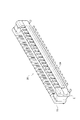
図1(a)は、本実施形態のヘッダ20の全体斜視図である。この図に示すように、ヘッダ20は、絶縁性の合成樹脂によって全体的に矩形状に型成形されたヘッダ成型品21を備えている。ヘッダ成型品21は、周縁部に沿って形成される周壁部23を備えている。ヘッダ成型品21の長辺方向には、所定ピッチpをもって複数のヘッダコンタクト22が装着されている。ヘッダコンタクト22は、所定厚さを持った帯状の金属材である。ヘッダコンタクト22の接続端子部22Tは周壁部23の下縁から外方に突出し、図示しない回路基板の導体パターンに半田付けされる。ヘッダ側面には、ヘッダ20とソケット10とを嵌合したときにソケット10に接する凸形状の凸部24が形成されている。
Fig.1 (a) is a whole perspective view of the
図1(b)は、本実施形態のソケット10の全体斜視図である。この図に示すように、ソケット10は、絶縁性の合成樹脂によって全体的にヘッダ成型品21と略相似の矩形状に型成形されたソケット成型品11を備えている。ソケット成型品11は、周縁部に沿って形成される周壁部13と、中央部に形成される島部14とを備えている。周壁部13と島部14との間には、ヘッダ20を嵌合する嵌合溝部15が形成されている。ソケット成型品11の長辺方向には、ヘッダコンタクト22のピッチpと等しいピッチpをもって複数のソケットコンタクト12が装着されている。ソケットコンタクト12は、ヘッダコンタクト22と同様に所定厚さを持った帯状の金属材である。ソケットコンタクト12の接続端子部12Tは周壁部13の下縁から外方に突出し、図示しない回路基板の導体パターンに半田付けされる。ここで、図中に太枠で示す面16は、嵌合状態でヘッダ20の凸部24と対向する面である。すなわち、図2に示すように、嵌合状態でヘッダ20が傾こうとしたとき、ヘッダ20の凸部24がソケット10の面16と接するようになっている。このようにすれば、凸部24が抵抗となるため、嵌合状態でぐらつきにくくすることができる。
FIG. 1B is an overall perspective view of the
図3は、本実施形態の別のヘッダ20の全体斜視図である。この図に示すように、ヘッダ20の凸部24は、ヘッダ側面の全体にわたって形成されている。このようにすれば、ソケット10と接する面積が増えるので、嵌合状態で更にぐらつきにくくすることができる。ただし、図中に丸印で示す領域Eについては、その上部の周壁部23が外方に突出しているため、凸部24を形成する必要はない。また、この図に示すように、凸部24のソケット10と接する箇所は、フラットな形状としてもよい。このようにすれば、ソケット10と接する面積が増えるので、嵌合状態で更にぐらつきにくくすることができる。
FIG. 3 is an overall perspective view of another
図4および図5は、本実施形態の別のコネクタを示す図である。すなわち、図4(a)は、ソケット10の全体斜視図、図4(b)は、ヘッダ20の全体斜視図である。また、図5(a)は、図4(a)に示すソケット10のA矢視拡大図、図5(b)は、図4(b)に示すヘッダ20のB矢視拡大図、図5(c)は、図4(a)に示すソケット10と図4(b)に示すヘッダ20の嵌合状態拡大図である。これらの図に示すように、凸部24のソケット10と接する箇所は、ソケット10側の形状を転写した形状としてもよい。すなわち、凸部24は、ソケット10側の凹部17を転写した形状となっている。このようにすれば、嵌合状態でソケット10の凹部17とヘッダ20の凸部24がかみ合うことになるため、嵌合状態で更にぐらつきにくくすることができる。
4 and 5 are diagrams showing another connector of the present embodiment. 4A is an overall perspective view of the
図6および図7は、ソケット10およびヘッダ20の具体例を示す図である。すなわち、図6(a)は、ソケット10の全体斜視図、図6(b)は、ヘッダ20の全体斜視図である。このヘッダ20としては、高さ1.0mm用ヘッダ20aと高さ1.5mm用ヘッダ20bの2種類があるものと仮定する。すなわち、図7(a)は、図6(a)に示すソケット10の断面図、図7(b)は、図6(b)に示す高さ1.0mm用ヘッダ20aの断面図、図7(c)は、図6(b)に示す高さ1.5mm用ヘッダ20bの断面図である。更に、ソケット10と高さ1.0mm用ヘッダ20aとを嵌合したときの断面図を図8(a)に、ソケット10と高さ1.5mm用ヘッダ20bとを嵌合したときの断面図を図8(b)に示す。これらの図に示すように、ソケット10側を共通としてヘッダ違いにより2種類以上の嵌合高さに対応することができる。高さ1.5mm用ヘッダ20bには凸部24が形成されている。高さ1.0mm用ヘッダ20aに凸部24を形成するかどうかは特に限定されるものではない。
6 and 7 are diagrams showing specific examples of the
以上のように、本実施形態のコネクタは、ヘッダ20とソケット10とを嵌合したときにソケット10に接する凸形状の凸部24をヘッダ側面に備える。これにより、ソケット10側を共通としてヘッダ違いにより2種類以上の嵌合高さに対応することができる場合でも嵌合状態でぐらつきにくいコネクタを提供することが可能である。
As described above, the connector of the present embodiment includes the
また、本実施形態のコネクタでは、凸部24は、ヘッダ側面の全体にわたって形成されている。これにより、ソケット10と接する面積が増えるので、嵌合状態で更にぐらつきにくくすることができる。
Moreover, in the connector of this embodiment, the
また、本実施形態のコネクタでは、凸部24のソケット10と接する箇所は、フラットな形状である。これにより、ソケット10と接する面積が増えるので、嵌合状態で更にぐらつきにくくすることができる。
Moreover, in the connector of this embodiment, the location which contact | connects the
また、本実施形態のコネクタでは、凸部24のソケット10と接する箇所は、ソケット10側の凹部17を転写した形状である。これにより、嵌合状態でソケット10の凹部17とヘッダ20の凸部24がかみ合うことになるため、嵌合状態で更にぐらつきにくくすることができる。しかも、凸部24の凸形状を凹部17の凹形状よりも若干大きくすれば、ヘッダ20とソケット10を嵌合したときに、凸形状と凹形状を圧入気味に噛み合わせることができる。このように圧入気味にすることで噛み合う力を更に大きくすることが可能になる。
Moreover, in the connector of this embodiment, the location which contact | connects the
なお、以上では好適な実施形態について説明したが、本発明は前記実施形態に限定されず、種々の変形が可能である。例えば、コネクタの成型品やコンタクト等の大きさや材質等のスペックは適宜変更することが可能である。 In addition, although preferred embodiment was described above, this invention is not limited to the said embodiment, A various deformation | transformation is possible. For example, the specifications such as the size and material of the molded product of the connector and the contact can be changed as appropriate.
10 ソケット
20 ヘッダ
24 凸部
10
Claims (8)
前記ヘッダと前記ソケットとを嵌合したときに前記ソケットに接する凸形状の凸部を前記ヘッダ側面に備え、
前記ソケットには前記ヘッダを嵌合する嵌合溝部が設けられ、前記ヘッダの周壁部が前記嵌合溝部に嵌合することを特徴とするコネクタ。 A connector for electrically connecting circuit boards by fitting a header and a socket,
Provided on the header side surface with a convex portion that contacts the socket when the header and the socket are fitted ,
The socket is provided with a fitting groove for fitting the header, and a peripheral wall of the header is fitted into the fitting groove .
Priority Applications (5)
| Application Number | Priority Date | Filing Date | Title |
|---|---|---|---|
| JP2010234718A JP5793660B2 (en) | 2010-10-19 | 2010-10-19 | Connector and header used for it |
| CN201180049546.0A CN103155293B (en) | 2010-10-19 | 2011-09-28 | Adapter and the plug piece used in the connector |
| PCT/JP2011/072191 WO2012053330A1 (en) | 2010-10-19 | 2011-09-28 | Connector and header used in same |
| US13/879,765 US9190751B2 (en) | 2010-10-19 | 2011-09-28 | Connector and header for use in the same |
| TW100135919A TWI533525B (en) | 2010-10-19 | 2011-10-04 | Connectors and plugs for use with the connector |
Applications Claiming Priority (1)
| Application Number | Priority Date | Filing Date | Title |
|---|---|---|---|
| JP2010234718A JP5793660B2 (en) | 2010-10-19 | 2010-10-19 | Connector and header used for it |
Publications (2)
| Publication Number | Publication Date |
|---|---|
| JP2012089337A JP2012089337A (en) | 2012-05-10 |
| JP5793660B2 true JP5793660B2 (en) | 2015-10-14 |
Family
ID=45975049
Family Applications (1)
| Application Number | Title | Priority Date | Filing Date |
|---|---|---|---|
| JP2010234718A Active JP5793660B2 (en) | 2010-10-19 | 2010-10-19 | Connector and header used for it |
Country Status (5)
| Country | Link |
|---|---|
| US (1) | US9190751B2 (en) |
| JP (1) | JP5793660B2 (en) |
| CN (1) | CN103155293B (en) |
| TW (1) | TWI533525B (en) |
| WO (1) | WO2012053330A1 (en) |
Families Citing this family (9)
| Publication number | Priority date | Publication date | Assignee | Title |
|---|---|---|---|---|
| US8888506B2 (en) * | 2013-01-29 | 2014-11-18 | Japan Aviation Electronics Industry, Limited | Connector |
| CN105684223B (en) * | 2013-10-31 | 2018-10-23 | 松下知识产权经营株式会社 | Socket, the connector for having the socket and the plug used in the connector |
| JP6388152B2 (en) * | 2014-08-07 | 2018-09-12 | パナソニックIpマネジメント株式会社 | Connector and header and socket used for the connector |
| JP6537890B2 (en) * | 2014-09-26 | 2019-07-03 | 日本航空電子工業株式会社 | connector |
| CN106486837B (en) * | 2015-08-25 | 2019-12-06 | 富泰华工业(深圳)有限公司 | Connector with a locking member |
| JP7341651B2 (en) * | 2018-10-24 | 2023-09-11 | ヒロセ電機株式会社 | Circuit board connector device |
| JP7270643B2 (en) * | 2020-03-13 | 2023-05-10 | サンウェイ コミュニケーション(ジアンスー) カンパニー リミテッド | RF connector with high transmission performance |
| JP1743539S (en) * | 2022-09-13 | 2023-11-10 | connector | |
| JP2024075983A (en) * | 2022-11-24 | 2024-06-05 | 日本航空電子工業株式会社 | Connector Assembly |
Family Cites Families (15)
| Publication number | Priority date | Publication date | Assignee | Title |
|---|---|---|---|---|
| US5478248A (en) | 1993-12-17 | 1995-12-26 | Berg Technology, Inc. | Connector for high density electronic assemblies |
| US5626482A (en) * | 1994-12-15 | 1997-05-06 | Molex Incorporated | Low profile surface mountable electrical connector assembly |
| US5830018A (en) * | 1995-12-12 | 1998-11-03 | Molex Incorporated | Low profile surface mountable electrical connector assembly |
| JP2002184521A (en) | 2000-12-18 | 2002-06-28 | Hirose Electric Co Ltd | Electrical connector |
| US6793506B1 (en) * | 2003-08-27 | 2004-09-21 | Molex Incorporated | Board-to-board electrical connector assembly |
| CN2735568Y (en) | 2004-08-27 | 2005-10-19 | 瀚宇电子股份有限公司 | Board-to-board connector |
| JP2006086083A (en) * | 2004-09-17 | 2006-03-30 | I-Pex Co Ltd | Connector |
| JP4287825B2 (en) * | 2005-01-28 | 2009-07-01 | モレックス インコーポレイテド | Board connector |
| CN101162806B (en) * | 2006-10-12 | 2011-01-12 | 富士康(昆山)电脑接插件有限公司 | Electrical connector |
| JP2008270085A (en) | 2007-04-24 | 2008-11-06 | Matsushita Electric Works Ltd | Connector |
| CN201048179Y (en) | 2007-05-25 | 2008-04-16 | 富港电子(东莞)有限公司 | Board-to-Board Connector |
| JP4809816B2 (en) * | 2007-08-31 | 2011-11-09 | パナソニック電工株式会社 | connector |
| JP4784673B2 (en) * | 2009-03-24 | 2011-10-05 | パナソニック電工株式会社 | connector |
| TWM371330U (en) | 2009-06-08 | 2009-12-21 | Hon Hai Prec Ind Co Ltd | Electrical connector |
| JP5049361B2 (en) * | 2010-02-10 | 2012-10-17 | パナソニック株式会社 | Sockets and connectors |
-
2010
- 2010-10-19 JP JP2010234718A patent/JP5793660B2/en active Active
-
2011
- 2011-09-28 CN CN201180049546.0A patent/CN103155293B/en active Active
- 2011-09-28 US US13/879,765 patent/US9190751B2/en not_active Expired - Fee Related
- 2011-09-28 WO PCT/JP2011/072191 patent/WO2012053330A1/en active Application Filing
- 2011-10-04 TW TW100135919A patent/TWI533525B/en active
Also Published As
| Publication number | Publication date |
|---|---|
| US9190751B2 (en) | 2015-11-17 |
| US20130217270A1 (en) | 2013-08-22 |
| WO2012053330A1 (en) | 2012-04-26 |
| CN103155293A (en) | 2013-06-12 |
| CN103155293B (en) | 2016-08-03 |
| JP2012089337A (en) | 2012-05-10 |
| TWI533525B (en) | 2016-05-11 |
| TW201230508A (en) | 2012-07-16 |
Similar Documents
| Publication | Publication Date | Title |
|---|---|---|
| JP5793660B2 (en) | Connector and header used for it | |
| JP4978313B2 (en) | connector | |
| US7985099B2 (en) | Electrical connector with improved housing background of the invention | |
| CN103259144B (en) | Connector and connector connecting body | |
| KR101021012B1 (en) | connector | |
| JP2012089336A (en) | Connector and socket used therefor | |
| JP4802959B2 (en) | connector | |
| US8052491B2 (en) | Electrical contact having upper contact with thickened base portion | |
| US8113884B2 (en) | Connector | |
| JP6761375B2 (en) | Electrical connector | |
| TWI506867B (en) | Electrical connector | |
| JP7507567B2 (en) | Plug Connector | |
| US20080026609A1 (en) | Low profile connector | |
| JP2012054215A (en) | Connector | |
| US11381013B2 (en) | Electrical connector | |
| JP6398354B2 (en) | connector | |
| US8366476B2 (en) | Electrical connector with improved alignment structure | |
| JP4658508B2 (en) | Terminal for electrical connection | |
| JP2010033714A (en) | Connector | |
| JP7561499B2 (en) | Plug Connector | |
| US7878867B2 (en) | Electrical contact having an upper contact with a thickened base portion | |
| JP2017147171A (en) | connector | |
| US20110281471A1 (en) | Electrical connector | |
| US20100035469A1 (en) | Connector | |
| US7413475B2 (en) | Electrical connector having ground planes |
Legal Events
| Date | Code | Title | Description |
|---|---|---|---|
| A621 | Written request for application examination |
Free format text: JAPANESE INTERMEDIATE CODE: A621 Effective date: 20130822 |
|
| A711 | Notification of change in applicant |
Free format text: JAPANESE INTERMEDIATE CODE: A711 Effective date: 20141009 |
|
| RD03 | Notification of appointment of power of attorney |
Free format text: JAPANESE INTERMEDIATE CODE: A7423 Effective date: 20141016 |
|
| A131 | Notification of reasons for refusal |
Free format text: JAPANESE INTERMEDIATE CODE: A131 Effective date: 20141104 |
|
| A521 | Written amendment |
Free format text: JAPANESE INTERMEDIATE CODE: A523 Effective date: 20141210 |
|
| TRDD | Decision of grant or rejection written | ||
| A01 | Written decision to grant a patent or to grant a registration (utility model) |
Free format text: JAPANESE INTERMEDIATE CODE: A01 Effective date: 20150217 |
|
| A61 | First payment of annual fees (during grant procedure) |
Free format text: JAPANESE INTERMEDIATE CODE: A61 Effective date: 20150312 |
|
| R151 | Written notification of patent or utility model registration |
Ref document number: 5793660 Country of ref document: JP Free format text: JAPANESE INTERMEDIATE CODE: R151 |