JP5774512B2 - Ranging device - Google Patents
Ranging device Download PDFInfo
- Publication number
- JP5774512B2 JP5774512B2 JP2012018123A JP2012018123A JP5774512B2 JP 5774512 B2 JP5774512 B2 JP 5774512B2 JP 2012018123 A JP2012018123 A JP 2012018123A JP 2012018123 A JP2012018123 A JP 2012018123A JP 5774512 B2 JP5774512 B2 JP 5774512B2
- Authority
- JP
- Japan
- Prior art keywords
- photoelectric conversion
- output
- pixel
- image sensor
- pixels
- Prior art date
- Legal status (The legal status is an assumption and is not a legal conclusion. Google has not performed a legal analysis and makes no representation as to the accuracy of the status listed.)
- Expired - Fee Related
Links
- 238000006243 chemical reaction Methods 0.000 claims description 69
- 238000003384 imaging method Methods 0.000 claims description 69
- 238000009825 accumulation Methods 0.000 claims description 45
- 238000012545 processing Methods 0.000 claims description 26
- 238000000034 method Methods 0.000 claims description 9
- 229960001716 benzalkonium Drugs 0.000 claims 1
- CYDRXTMLKJDRQH-UHFFFAOYSA-N benzododecinium Chemical compound CCCCCCCCCCCC[N+](C)(C)CC1=CC=CC=C1 CYDRXTMLKJDRQH-UHFFFAOYSA-N 0.000 claims 1
- 230000002194 synthesizing effect Effects 0.000 description 40
- 238000010586 diagram Methods 0.000 description 19
- 230000015654 memory Effects 0.000 description 14
- 229920006395 saturated elastomer Polymers 0.000 description 12
- 230000015572 biosynthetic process Effects 0.000 description 11
- 238000011156 evaluation Methods 0.000 description 11
- 238000003786 synthesis reaction Methods 0.000 description 11
- 238000001514 detection method Methods 0.000 description 10
- 238000005259 measurement Methods 0.000 description 10
- 230000003287 optical effect Effects 0.000 description 6
- 230000006835 compression Effects 0.000 description 4
- 238000007906 compression Methods 0.000 description 4
- 230000035945 sensitivity Effects 0.000 description 4
- 238000012935 Averaging Methods 0.000 description 2
- 230000007423 decrease Effects 0.000 description 2
- 230000003111 delayed effect Effects 0.000 description 2
- 238000012546 transfer Methods 0.000 description 2
- 101000863856 Homo sapiens Shiftless antiviral inhibitor of ribosomal frameshifting protein Proteins 0.000 description 1
- 230000000295 complement effect Effects 0.000 description 1
- 230000006866 deterioration Effects 0.000 description 1
- 230000000694 effects Effects 0.000 description 1
- 230000006870 function Effects 0.000 description 1
- 229910044991 metal oxide Inorganic materials 0.000 description 1
- 150000004706 metal oxides Chemical class 0.000 description 1
- 238000012986 modification Methods 0.000 description 1
- 230000004048 modification Effects 0.000 description 1
- 239000004065 semiconductor Substances 0.000 description 1
Images


Classifications
-
- G—PHYSICS
- G01—MEASURING; TESTING
- G01C—MEASURING DISTANCES, LEVELS OR BEARINGS; SURVEYING; NAVIGATION; GYROSCOPIC INSTRUMENTS; PHOTOGRAMMETRY OR VIDEOGRAMMETRY
- G01C3/00—Measuring distances in line of sight; Optical rangefinders
- G01C3/10—Measuring distances in line of sight; Optical rangefinders using a parallactic triangle with variable angles and a base of fixed length in the observation station, e.g. in the instrument
- G01C3/18—Measuring distances in line of sight; Optical rangefinders using a parallactic triangle with variable angles and a base of fixed length in the observation station, e.g. in the instrument with one observation point at each end of the base
-
- G—PHYSICS
- G03—PHOTOGRAPHY; CINEMATOGRAPHY; ANALOGOUS TECHNIQUES USING WAVES OTHER THAN OPTICAL WAVES; ELECTROGRAPHY; HOLOGRAPHY
- G03B—APPARATUS OR ARRANGEMENTS FOR TAKING PHOTOGRAPHS OR FOR PROJECTING OR VIEWING THEM; APPARATUS OR ARRANGEMENTS EMPLOYING ANALOGOUS TECHNIQUES USING WAVES OTHER THAN OPTICAL WAVES; ACCESSORIES THEREFOR
- G03B13/00—Viewfinders; Focusing aids for cameras; Means for focusing for cameras; Autofocus systems for cameras
- G03B13/32—Means for focusing
- G03B13/34—Power focusing
- G03B13/36—Autofocus systems
-
- H—ELECTRICITY
- H04—ELECTRIC COMMUNICATION TECHNIQUE
- H04N—PICTORIAL COMMUNICATION, e.g. TELEVISION
- H04N25/00—Circuitry of solid-state image sensors [SSIS]; Control thereof
- H04N25/50—Control of the SSIS exposure
- H04N25/53—Control of the integration time
- H04N25/533—Control of the integration time by using differing integration times for different sensor regions
-
- H—ELECTRICITY
- H04—ELECTRIC COMMUNICATION TECHNIQUE
- H04N—PICTORIAL COMMUNICATION, e.g. TELEVISION
- H04N25/00—Circuitry of solid-state image sensors [SSIS]; Control thereof
- H04N25/50—Control of the SSIS exposure
- H04N25/57—Control of the dynamic range
- H04N25/58—Control of the dynamic range involving two or more exposures
- H04N25/581—Control of the dynamic range involving two or more exposures acquired simultaneously
- H04N25/583—Control of the dynamic range involving two or more exposures acquired simultaneously with different integration times
Landscapes
- Physics & Mathematics (AREA)
- Engineering & Computer Science (AREA)
- General Physics & Mathematics (AREA)
- Multimedia (AREA)
- Signal Processing (AREA)
- Radar, Positioning & Navigation (AREA)
- Electromagnetism (AREA)
- Remote Sensing (AREA)
- Solid State Image Pick-Up Elements (AREA)
- Transforming Light Signals Into Electric Signals (AREA)
- Lens Barrels (AREA)
- Automatic Focus Adjustment (AREA)
- Measurement Of Optical Distance (AREA)
- Studio Devices (AREA)
- Focusing (AREA)
Description
本発明の実施形態は、測距装置に関する。 Embodiments described herein relate generally to a distance measuring device.
測定対象とする物体までの距離を測定する測距装置としては、例えば、位相差検出方式によるものが知られている。位相差検出方式では、同一の物体を異なる位置において撮影して得られた被写体像の位相差を検出し、その位相差に基づいて、物体までの距離を算出する。被写体像の撮影には、電荷蓄積型の光電変換素子を備える固体撮像装置を使用する。電荷蓄積型の光電変換素子を使用する測距装置では、電荷の蓄積時間を適切に制御しなければ、光電変換による出力がほとんど得られない場合や、入射光量に対して出力が飽和してしまう場合がある。この場合、物体までの正確な距離を検出することが困難となる。 As a distance measuring device for measuring a distance to an object to be measured, for example, a device using a phase difference detection method is known. In the phase difference detection method, a phase difference between subject images obtained by photographing the same object at different positions is detected, and a distance to the object is calculated based on the phase difference. A solid-state imaging device having a charge storage type photoelectric conversion element is used for photographing a subject image. In a distance measuring device that uses a charge storage type photoelectric conversion element, if the charge storage time is not properly controlled, almost no output can be obtained by photoelectric conversion, or the output is saturated with respect to the amount of incident light. There is a case. In this case, it is difficult to detect an accurate distance to the object.
このような不具合を回避するには、例えば、複数の分割領域に最適な蓄積時間を設定し、複数回画像データを読み出す措置を取り得る。例えば、カメラの焦点調節装置等、調節の高速化が求められる場合に、測距装置は、高速な距離測定が必要となる。電荷蓄積型の光電変換素子を備える固体撮像装置は、出力の読み出しを一部の分割領域に限定可能とすることで、読み出し処理の高速化を図り得る一方、複数回の電荷蓄積を要することで、高速な位相差検出が困難となる。 In order to avoid such a problem, for example, it is possible to set an optimum accumulation time for a plurality of divided regions and take measures to read the image data a plurality of times. For example, when a high-speed adjustment is required, such as a camera focus adjustment device, the distance measurement device requires high-speed distance measurement. A solid-state imaging device including a charge storage type photoelectric conversion element can speed up the readout process by enabling output readout to be limited to a part of the divided areas, while requiring multiple times of charge accumulation. High-speed phase difference detection becomes difficult.
本発明の一つの実施形態は、物体までの距離の正確かつ高速な測定を可能とする測距装置を提供することを目的とする。 An object of one embodiment of the present invention is to provide a distance measuring device that enables accurate and high-speed measurement of a distance to an object.
本発明の一つの実施形態によれば、測距装置は、固体撮像装置を備える。固体撮像装置は、第1のイメージセンサ、第2のイメージセンサ及び撮像処理回路を有する。第1のイメージセンサは、被写体像を取り込む。第2のイメージセンサは、第1のイメージセンサと並べて設けられている。第2のイメージセンサは、第1のイメージセンサで取り込まれる被写体像に対し位相差を持たせた被写体像を取り込む。撮像処理回路は、第1のイメージセンサにより取得された被写体像と、第2のイメージセンサにより取得された被写体像と、を出力する。第1のイメージセンサ及び第2のイメージセンサには、それぞれ複数の光電変換部が配列されている。光電変換部は、いずれも、第1画素からなるラインと、第2画素からなるラインと、を交互に並列させて構成されている。第2画素は、第1画素に対し電荷の蓄積時間が短く設定されている。撮像処理回路は、出力合成部を有する。出力合成部は、第1画素による出力と第2画素による出力とを合成する。出力合成部は、入射光量に対する出力の飽和が生じている第1画素について、第2画素による検出結果を使用して出力を補間する。 According to one embodiment of the present invention, the distance measuring device includes a solid-state imaging device. The solid-state imaging device includes a first image sensor, a second image sensor, and an imaging processing circuit. The first image sensor captures a subject image. The second image sensor is provided side by side with the first image sensor. The second image sensor captures a subject image having a phase difference with respect to the subject image captured by the first image sensor. The imaging processing circuit outputs the subject image acquired by the first image sensor and the subject image acquired by the second image sensor. A plurality of photoelectric conversion units are arranged in each of the first image sensor and the second image sensor. Each of the photoelectric conversion units is configured by alternately arranging lines composed of first pixels and lines composed of second pixels. The second pixel has a shorter charge accumulation time than the first pixel. The imaging processing circuit has an output combining unit. The output combining unit combines the output from the first pixel and the output from the second pixel. The output combining unit interpolates the output using the detection result of the second pixel for the first pixel in which the output is saturated with respect to the incident light amount.
以下に添付図面を参照して、実施形態にかかる測距装置を詳細に説明する。なお、これらの実施形態により本発明が限定されるものではない。 Hereinafter, a distance measuring apparatus according to an embodiment will be described in detail with reference to the accompanying drawings. Note that the present invention is not limited to these embodiments.
(第1の実施形態)
図1は、第1の実施形態にかかる測距装置に備えられた固体撮像装置の概略構成を示す模式図である。図2は、図1に示す固体撮像装置を備える測距装置の概略構成を示すブロック図である。測距装置1は、例えば、カメラの焦点調節装置等に適用される。
(First embodiment)
FIG. 1 is a schematic diagram illustrating a schematic configuration of a solid-state imaging device provided in the distance measuring device according to the first embodiment. FIG. 2 is a block diagram showing a schematic configuration of a distance measuring device including the solid-state imaging device shown in FIG. The distance measuring
測距装置1は、レンズモジュール2、固体撮像装置3及びCPU4を有する。レンズモジュール2は、測定対象とする物体からの光を取り込み、その物体の像を被写体像として結像させる。固体撮像装置3は、レンズモジュール2により取り込まれた光を信号電荷に変換し、被写体像を撮像する。CPU4は、固体撮像装置3にて撮像された被写体像の位相差に基づいて、物体までの距離を算出する。
The
固体撮像装置3は、ラインセンサ11及び12、セレクタ13及び撮像処理回路14を有する。ラインセンサ11は、被写体像を取り込む第1のイメージセンサである。ラインセンサ12は、ラインセンサ11と並べて設けられた第2のイメージセンサである。ラインセンサ12は、ラインセンサ11で取り込まれる被写体像に対し位相差を持たせた被写体像を取り込む。
The solid-
ラインセンサ11及び12は、例えば、CMOS(complementary metal oxide semiconductor)イメージセンサである。ラインセンサ11及び12としては、CMOSイメージセンサに代えて、CCD(charge coupled device)を適用しても良い。
The
ラインセンサ11及び12は、それぞれ、複数の光電変換部15、カラム型ADC(アナログデジタル変換器)17及び水平転送部18を有する。ラインセンサ11及び12には、複数の光電変換部15が水平方向に配列されている。各光電変換部15は、複数の画素16を備える。
Each of the
カラム型ADC17は、画素16から垂直読み出しライン(図示省略)まで転送された信号を、アナログ方式からデジタル方式へ変換する。水平転送部18は、カラム型ADC17にてデジタル方式へ変換された信号を順次読み出す。
The
セレクタ13は、ラインセンサ11からの信号とラインセンサ12からの信号とを順次切り換えて、撮像処理回路14へ出力する。撮像処理回路14は、ラインセンサ11により取得された被写体像の信号と、ラインセンサ12により取得された被写体像の信号と、について信号処理を実施し、CPU4へ出力する。撮像処理回路14は、ハイダイナミックレンジ(high dynamic range;HDR)合成のためのHDR合成部19、及び出力加算部20を有する。
The
HDR合成部19は、電荷の蓄積時間が互いに異なる画素による出力を、光電変換部15ごとに合成する出力合成部として機能する。出力加算部20は、各画素16についてのHDR合成部19からの出力を光電変換部15ごとに加算し、光電変換部15ごとの出力とする。
The HDR synthesizing
固体撮像装置3は、セレクタ13で選択された信号をいずれも同じ撮像処理回路14へ入力する構成に限られない。固体撮像装置3は、ラインセンサ11に対応する撮像処理回路14と、ラインセンサ12に対応する撮像処理回路14とを設ける構成としても良い。
The solid-
図3は、光電変換部の構成を説明する図である。ラインセンサ11及び12に設けられた複数の光電変換部15は、水平方向であるX方向に配列されている。複数の光電変換部15は、いずれも、X方向と、垂直方向であるY方向とに配列された複数の画素16により構成されている。
FIG. 3 is a diagram illustrating the configuration of the photoelectric conversion unit. The plurality of
本実施形態では、画素16は、各光電変換部15において、例えば、X方向に5個(m=5)、Y方向に10個(n=10)のアレイ状に配置されている。ラインセンサ11及び12において、配列させる光電変換部15の数は同一であるものとする。各光電変換部15の画素16の数は、いずれも同一であるものとする。なお、光電変換部15において、X方向へ配列させる画素16の個数mは少なくとも1、Y方向へ配列させる画素16の個数nは少なくとも2、であれば良く、いずれも適宜変更可能であるものとする。
In the present embodiment, in each
固体撮像装置3は、各光電変換部15において、X方向へ並列させた画素16からなるラインごとに、電荷の蓄積時間を、例えば、A及びA/2と交互に異ならせる制御を実施する。
The solid-
図4は、測距装置による位相差の検出と、距離の算出とを説明する図である。レンズモジュール2は、撮像レンズ21及び22を備える。撮像レンズ21は、ラインセンサ11に対向させて設けられている。撮像レンズ22は、ラインセンサ12に対向させて設けられている。撮像レンズ21及び22は、撮像レンズ21の光軸23及び撮像レンズ22の光軸24に対して垂直な方向へ並べられている。
FIG. 4 is a diagram for explaining phase difference detection and distance calculation by the distance measuring device. The
撮像レンズ21は、測定対象とする物体25からの光を取り込み、ラインセンサ11へ入射させる。撮像レンズ21は、物体25の像である被写体像をラインセンサ11に結像させる。撮像レンズ22は、物体25からの光を取り込み、ラインセンサ12へ入射させる。撮像レンズ22は、ラインセンサ12に被写体像を結像させる。
The
物体25が無限遠にあると仮定した場合、ラインセンサ11及び12において、被写体像はそれぞれ光軸23及び24上に結像する。物体25が有限遠或いは中近距離にあると仮定した場合において、被写体像は、ラインセンサ11では光軸23上に結像するのに対し、ラインセンサ12では光軸24に対し位相差αだけずれた位置に結像する。測距装置1は、例えば、以下に説明する三角測距法により、観測点から物体25までの距離を測定する。
Assuming that the
CPU4は、かかる位相差αを実際の距離に変換するための演算を実施する。距離LCと光軸23及び24間の長さkとを辺とする三角形と、焦点距離fと位相差αとを辺とする三角形とは、相似の関係にある。従って、距離LCは、以下の式(1)により求められる。
LC=f×k/α ・・・(1)
The
LC = f × k / α (1)
長さk及び焦点距離fは、いずれもレンズモジュール2の構成により定められた値であることから、CPU4は、位相差αを求めて式(1)に代入することで、距離LCを算出できる。
Since the length k and the focal length f are both values determined by the configuration of the
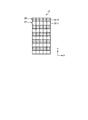
図5は、位相差の検出について説明する図である。CPU4は、例えば、ラインセンサ11のうち基準とする領域26の光電変換部15からの出力群1F〜1Iが、ラインセンサ12からの出力では、光電変換部15を単位としていくつ分ずれているかを検出する。
FIG. 5 is a diagram for explaining detection of the phase difference. For example, the
CPU4は、ラインセンサ11のうち基準とする領域26と同じ位置の領域27−1における、ラインセンサ12の出力群1D〜1Gを参照する。CPU4は、ラインセンサ11からの出力群1F〜1Iとラインセンサ12の出力群1D〜1Gとを光電変換部15ごとに比較し、光電変換部15ごとの出力の差分を求める。CPU4は、光電変換部15ごとに求めた差分の絶対値を合計する。CPU4は、かかる合計結果を、被写体像のずれを検出するための評価値として保持する。
The
次に、CPU4は、領域27−1から光電変換部15一つ分移動した領域27−2における、ラインセンサ12の出力群1E〜1Hを参照する。CPU4は、ラインセンサ11からの出力群1F〜1Iとラインセンサ12の出力群1E〜1Hとについて、光電変換部15ごとの出力の差分を求める。CPU4は、光電変換部15ごとに求めた差分の絶対値を合計し、評価値とする。CPU4は、このようにして、ラインセンサ12において出力群を参照する領域を移動させながら、評価値を求めていく。
Next, the
ラインセンサ11及び12について、光電変換部15ごとの出力が一致している場合、評価値は理論上ゼロとなる。評価値がゼロとなるときにおける、ラインセンサ11のうち基準とする領域26と、ラインセンサ12のうち出力を参照した領域とのずれ量が、位相差αに相当する。ただし、実際の評価値は、ノイズ等の影響によりゼロより若干大きい値となることから、CPU4は、評価値が最小となるときのずれ量を、位相差αとする。なお、ラインセンサ11のうち基準とする領域26と同じ位置の領域27−1において、評価値が最小となった場合、位相差は生じておらず、物体25は無限遠に存在していることとなる。
For the
図5に示す例では、ラインセンサ11のうち基準とする領域26と、ラインセンサ12のうち領域27−1から光電変換部15二つ分移動した領域27−3とで、出力群1F〜1Iが一致し、評価値が最小となる。この場合、位相差αは、光電変換部15二つ分の長さとなる。
In the example illustrated in FIG. 5, the
なお、CPU4は、光電変換部15の長さを単位として位相差αを検出する場合に限られない。CPU4は、位相差αとして、光電変換部15の長さ未満のずれも含めて検出するものとしても良い。CPU4は、例えば、各評価値のうち最も小さい二つの値を使用する線形補間により、評価値が極小となるときのずれ量を、位相差αとして求める。CPU4は、従来の相関演算及び補間演算のいずれを用いて、位相差αを算出するものとしても良い。
The
本実施形態では、固体撮像装置3は、光電変換部15を構成するm×n個の画素16による出力を用いて、光電変換部15の出力を求める。
In the present embodiment, the solid-
図6は、光電変換部を構成する画素の配列について説明する図である。固体撮像装置3は、ラインセンサ11及び12の各光電変換部15を、いずれも、電荷の蓄積時間を互いに異ならせた画素16−1及び16−2を含めた構成とすることで、HDRを実現可能とする。
FIG. 6 is a diagram for explaining an arrangement of pixels constituting the photoelectric conversion unit. The solid-
画素16−1は、例えば、電荷の蓄積時間がAと設定されている。画素16−2は、電荷の蓄積時間が、例えば、画素16−1の蓄積時間Aに対し半分のA/2と設定されている。ライン31は、画素16−1をX方向へ並列させて構成されている。ライン32は、画素16−2をX方向へ並列させて構成されている。
In the pixel 16-1, for example, the charge accumulation time is set to A. In the pixel 16-2, for example, the charge accumulation time is set to A / 2 that is half the accumulation time A of the pixel 16-1. The
ライン31及び32は、Y方向において交互に配置されている。固体撮像装置3は、ライン31及び32の配置に応じて、電荷の蓄積時間をA及びA/2と交互に異ならせて、ラインセンサ11及び12を駆動する。なお、光電変換部15は、X方向のラインごとに電荷の蓄積時間を異ならせる構成に代えて、Y方向のカラムごとに電荷の蓄積時間を異ならせる構成としても良い。
The
図7は、被写体像の輝度分布と、電荷の蓄積時間を異ならせた画素による出力との関係を説明する図である。図7に示す各グラフの縦軸は輝度、横軸は被写体像における位置を表すものとする。例えば、被写体像が、図7の上段に示す輝度分布を持つものとする。 FIG. 7 is a diagram for explaining the relationship between the luminance distribution of the subject image and the output from the pixels with different charge accumulation times. The vertical axis of each graph shown in FIG. 7 represents the luminance, and the horizontal axis represents the position in the subject image. For example, it is assumed that the subject image has a luminance distribution shown in the upper part of FIG.
図7の中段は、上段に示す輝度分布の被写体像を、蓄積時間を長時間とした画素を用いて検出した場合を表している。この場合、被写体像のうち輝度が低い部分については、高い感度で検出可能である。その一方、輝度が高い部分については、例えば所定の輝度L以上において、入射光量に対する信号出力の飽和が生じることがある。このような出力の飽和が生じると、測距装置1は、距離の正確な測定が困難となる。
The middle part of FIG. 7 represents a case where the subject image having the luminance distribution shown in the upper part is detected using pixels with a long accumulation time. In this case, a low luminance portion of the subject image can be detected with high sensitivity. On the other hand, for a portion with high luminance, signal output may be saturated with respect to the amount of incident light, for example, at a predetermined luminance L or higher. When such output saturation occurs, it becomes difficult for the
図7の下段は、上段に示す輝度分布の被写体像を、蓄積時間を短時間とした画素を用いて検出した場合を表している。この場合、被写体像のうち輝度が高い部分については、出力の飽和が生じにくくなる。その一方、輝度が低い部分については、出力レベルがさらに低下するために、信号対ノイズ比(SNR)が悪化することとなる。測距装置1は、SNRの悪化により、位相差の検出精度が低下することとなる。
The lower part of FIG. 7 represents a case where the subject image having the luminance distribution shown in the upper part is detected using pixels whose accumulation time is short. In this case, output saturation is less likely to occur in a portion of the subject image having high luminance. On the other hand, the signal-to-noise ratio (SNR) is deteriorated in the portion where the luminance is low because the output level further decreases. In the
図8は、第1の実施形態におけるラインセンサの出力特性を説明する図である。図8に示すグラフの縦軸は出力、横軸は輝度を表すものとする。輝度が低い部分については、蓄積時間をA(長時間)とした画素16−1は、蓄積時間をA/2(短時間)とした画素16−2に比べて、入射光量に対する出力の割合が高くなることで、明暗差が良好な輝度情報を得ることが可能である。画素16−1は、所定の輝度L以上において出力が飽和し、輝度が増加しても一定の出力Sしか得られないこととなる。画素16−2は、通常の照度環境下では画素16−1のような出力の飽和を生じさせず、入射光量に応じた出力を得ることができる。 FIG. 8 is a diagram illustrating the output characteristics of the line sensor according to the first embodiment. In the graph shown in FIG. 8, the vertical axis represents output and the horizontal axis represents luminance. For the portion with low luminance, the pixel 16-1 with an accumulation time of A (long time) has a higher output ratio to the incident light amount than the pixel 16-2 with an accumulation time of A / 2 (short time). By increasing the luminance information, it is possible to obtain luminance information with a good contrast. In the pixel 16-1, the output is saturated at a predetermined luminance L or higher, and only a constant output S can be obtained even if the luminance increases. The pixel 16-2 can obtain an output corresponding to the amount of incident light without causing output saturation like the pixel 16-1 under a normal illuminance environment.
撮像処理回路14は、輝度がL以下である部分については画素16−1の出力を使用し、輝度がLより大きい部分については画素16−2の出力を使用して、光電変換部15の出力を求める。固体撮像装置3は、輝度が低い部分についての画素16−1の出力と、輝度が高い部分についての画素16−2の出力とをHDR合成部19において合成することにより、HDRによる撮像ができる。
The imaging processing circuit 14 uses the output of the pixel 16-1 for a portion where the luminance is L or less, and uses the output of the pixel 16-2 for a portion where the luminance is greater than L, and outputs the output of the
HDR合成部19は、画素16−1の出力に合わせて、画素16−2の出力をゲイン倍、この例では2倍として、画素16−1及び16−2の出力を合成する。固体撮像装置3は、互いに同じ感度の画素16−1及び16−2に対し、蓄積時間をA及びA/2と異ならせることで、2倍のダイナミックレンジを得ることが可能となる。
The
なお、通常のAD変換における分解能が10ビットである場合に、撮像処理回路14の出力は、HDR合成を経ることで11ビットとなる。撮像処理回路14は、HDR合成を経た信号について圧縮処理を施すことで、HDR合成前のビット数へ信号を変換することとしても良い。これにより、CPU4は、HDR合成を経ない従来の場合と同様の演算処理を適用することが可能となる。撮像処理回路14は、かかる圧縮処理を行わず、ビット数が増加したままの信号をCPU4へ入力することとしても良い。
Note that when the resolution in normal AD conversion is 10 bits, the output of the imaging processing circuit 14 becomes 11 bits through the HDR synthesis. The imaging processing circuit 14 may convert the signal to the number of bits before HDR synthesis by performing compression processing on the signal that has undergone HDR synthesis. As a result, the
図9は、HDR合成の具体的な方法について説明する図である。HDR合成部19は、画素16−1の出力と、画素16−2の出力を2倍としたものとを合成する。また、例えば、ライン31のうち、図中白抜きで表す五つの画素16−1に出力の飽和が生じていたとする。
FIG. 9 is a diagram for explaining a specific method of HDR synthesis. The
HDR合成部19は、入射光量に対する出力の飽和が生じている画素16−1について、画素16−2による検出結果を使用して出力を補間する。この場合、HDR合成部19は、飽和が生じた画素16−1ごとに、当該画素16−1の上下に位置する二つの画素16−2の出力を平均し、さらに2倍とする演算を実施する。このようにして、HDR合成部19は、飽和が生じた画素16−1について、それぞれ出力を補間する。なお、画素16−1についての出力の補間のための演算は、この例による場合に限られず、いずれの手法によるものであっても良いものとする。
The
測距装置1は、固体撮像装置3におけるHDR合成により、入射光量に対する出力の飽和を抑制させ、距離の正確な測定が可能となる。また、測距装置1は、輝度が低い場合であっても高い感度で輝度情報が得られ、位相差の高精度な検出が可能となる。
The
図10は、HDR合成部が備える回路構成の例を示すブロック図である。HDR合成部19は、セレクタ41及び42、ラインメモリ(1H)43及び44、飽和判定部45及びラインカウンタ46を有する。
FIG. 10 is a block diagram illustrating an example of a circuit configuration included in the HDR synthesis unit. The
ラインカウンタ46は、HDR合成部19へ入力された信号47がライン31及び32のいずれからの出力であるかを示す信号を出力する。ラインカウンタ46は、信号47がライン31からの出力である場合、例えば「0」を出力する。ラインカウンタ46は、信号47がライン32からの出力である場合、例えば「1」を出力する。ラインカウンタ46からの出力は、セレクタ41における選択制御入力信号とされる。
The
セレクタ41には、ゲインNの乗算を経た信号47と、ゲインNの乗算を経ていない信号47とが入力される。セレクタ41は、選択制御入力信号である「0」が入力された場合、ゲインNの乗算を経ていない信号47を選択する。セレクタ41は、選択制御入力信号である「1」が入力された場合、ゲインNの乗算を経た信号47を選択する。これにより、HDR合成部19は、蓄積時間をAとした画素16−1からの出力と、蓄積時間をA/2とした画素16−2からの出力とのレベルを合わせる。この例では、N=2とする。
The
ラインメモリ43及び44は、セレクタ41からの信号を1ラインずつ遅延させる。飽和判定部45は、ラインメモリ43から読み出された信号を対象として、入射光量に対する出力の飽和が画素16に生じているか否かの飽和判定を実施する。飽和判定部45は、ラインメモリ43から読み出された信号と、予め設定された飽和判定用閾値48との比較により、飽和が生じているか否かを判定する。
The
飽和判定部45は、飽和が生じていると判定した場合、その旨を表す信号、例えば「1」を、判定結果として出力する。飽和判定部45は、飽和が生じていないと判定した場合、その旨を表す信号、例えば「0」を、判定結果として出力する。
When the
飽和判定部45による判定結果は、ラインカウンタ46からの信号を反転させた信号との論理積として、セレクタ42へ入力される。ラインカウンタ46からの信号を反転させた信号は、ラインメモリ43から読み出された信号が、ライン31及び32のいずれからの出力であるかを示す。
The determination result by the
これにより、ラインメモリ43から読み出された信号がライン31からの出力であって、かつ画素16−1に飽和が生じている場合に、セレクタ42には「1」が入力される。ラインメモリ43から読み出された信号がライン31からの出力であって、かつ画素16−1に飽和が生じていない場合、セレクタ42には「0」が入力される。さらに、ラインメモリ43から読み出された信号がライン32からの出力である場合、セレクタ42には「0」が入力される。これらの信号は、セレクタ42における選択制御入力信号とされる。
As a result, when the signal read from the
HDR合成部19は、セレクタ41からの遅延前の信号と、ラインメモリ44から読み出した信号とを加算及び2分の1倍とすることで、両信号の平均値を求める。セレクタ42には、かかる平均値と、ラインメモリ43から読み出された信号とが入力される。
The
セレクタ42は、選択制御入力信号である「1」が入力された場合、セレクタ41からの信号とラインメモリ44から読み出された信号との平均値を選択する。これにより、HDR合成部19は、飽和が生じている画素16−1については、当該画素16−1の上下に位置する二つの画素16−2からの出力の平均値に置き換えることで、出力を補間する。
When the selection control input signal “1” is input, the
セレクタ42は、選択制御入力信号である「0」が入力された場合、ラインメモリ43から読み出された信号を選択する。これにより、HDR合成部19は、飽和が生じていない画素16−1及び16−2からの信号については、補間を実施せず出力する。
The
HDR合成部19は、セレクタ42で選択された信号を出力する。このようにして、HDR合成部19は、画素16−1及び16−2による出力を合成する。なお、HDR合成部19は、飽和が生じている画素16−1について、上下の二本のライン32における画素16−2からの出力の平均値への置き換えを実施する場合に限られない。HDR合成部19は、飽和が生じている画素16−1について、いずれの手法により出力を補間することとしても良い。
The
HDR合成部19は、例えば、飽和が生じている画素16−1に対し、上下の二本のライン32のうち一方における画素16−2の出力への置き換えを実施することとしても良い。この場合、HDR合成部19は、簡易な演算による補間を可能とすることで、回路構成の小規模化を図り得る。
For example, the
撮像処理回路14は、HDR合成部19から出力された信号について圧縮処理を施すこととしても良い。例えば、上述のHDR合成部19は、デジタルレンジを1ビット増加させる。撮像処理回路14は、例えばガンマ変換回路を用いて、圧縮処理を施す。
The imaging processing circuit 14 may perform compression processing on the signal output from the
図11は、出力加算部が備える回路構成の例を示すブロック図である。出力加算部20は、HDR合成部19から入力されラインメモリ51にて遅延させた信号と、遅延前の信号とを加算していく。出力加算部20は、制御カウンタ52からの垂直カウントに応じて、垂直方向について画素16−1及び16−2の出力を加算する。出力加算部20は、制御カウンタ52からの水平カウントに応じて、さらに水平方向について出力を加算する。出力加算部20は、かかる加算結果を、光電変換部15ごとの出力とする。
FIG. 11 is a block diagram illustrating an example of a circuit configuration included in the output addition unit. The
このように、測距装置1は、固体撮像装置3におけるHDR合成により、物体25までの距離を正確に測定可能とする。また、測距装置1は、固体撮像装置3において複数回の電荷蓄積を要する場合に比べ、高速な位相差検出が可能となる。測距装置1は、固体撮像装置3を適用することで、物体までの距離を正確かつ高速に測定することができる。
As described above, the
(第2の実施形態)
図12は、第2の実施形態にかかる測距装置に備えられた固体撮像装置のうち、ラインセンサに設けられた光電変換部の概略構成を示す図である。第1の実施形態と同一の部分には同一の符号を付し、重複する説明を適宜省略する。
(Second Embodiment)
FIG. 12 is a diagram illustrating a schematic configuration of the photoelectric conversion unit provided in the line sensor in the solid-state imaging device provided in the distance measuring apparatus according to the second embodiment . The same parts as those in the first embodiment are denoted by the same reference numerals, and repeated description will be omitted as appropriate.
第2の実施形態にかかる固体撮像装置において、光電変換部60は、電荷の蓄積時間を互いに異ならせた四本のライン61−1、61−2、61−3及び61−4を周期的に並列させて構成されている。光電変換部60において、画素16は、例えば、X方向に12個(m=12)、Y方向に12個(n=12)のアレイ状に配置されている。
In the solid-state imaging device according to the second embodiment, the
固体撮像装置は、X方向へ並列させた画素16からなるラインごとに、電荷の蓄積時間を、例えば、A、A/2、A/4及びA/8と周期的に異ならせる制御を実施する。ライン61−1は、蓄積時間がAとされたラインとする。ライン61−2は、蓄積時間がA/2とされたラインとする。ライン61−3は、蓄積時間がA/4とされたラインとする。ライン61−4は、蓄積時間がA/8とされたラインとする。
The solid-state imaging device performs control so that the charge accumulation time is periodically different from, for example, A, A / 2, A / 4, and A / 8 for each line including the
図13は、HDR合成部が備える回路構成の例を示すブロック図である。HDR合成部62は、ライン61−1の画素16に合わせて、ライン61−2、61−3及び61−4の画素16の出力をゲイン倍、この例ではそれぞれ2倍、4倍及び8倍として、各ライン61−1〜61−4の出力を合成する。第2の実施形態にかかる固体撮像装置は、互いに同じ感度の画素16に対し、ライン61−1〜61−4ごとに蓄積時間をA、A/2、A/4及びA/8と異ならせることで、最大で8倍のダイナミックレンジを得ることが可能となる。
FIG. 13 is a block diagram illustrating an example of a circuit configuration included in the HDR synthesis unit. The HDR synthesizing unit 62 multiplies the output of the
飽和判定部63は、HDR合成部62へ入力された信号を対象として、入射光量に対する出力の飽和が画素16に生じているか否かの飽和判定を実施する。飽和判定部63は、HDR合成部62へ入力された信号と、予め設定された飽和判定用閾値48との比較により、飽和が生じているか否かを判定する。飽和判定部63は、飽和が生じていないと判定した場合に、飽和判定の対象とした信号を出力する。
The
HDR合成部62は、ライン61−2、61−3及び61−4から入力され、飽和が生じていないと判定された信号については、ゲイン倍、この例ではそれぞれ2倍、4倍及び8倍とする。HDR合成部62は、制御カウンタ65からの垂直カウントに応じて、HDR合成部62へ入力された信号がいずれのライン61−1〜61−4からの出力であるかを識別し、ゲインを適宜乗算する。
The HDR synthesizing unit 62 is input from the lines 61-2, 61-3, and 61-4, and for the signal determined not to be saturated, the gain is multiplied by 2 times, 4 times, and 8 times in this example, respectively. And The HDR synthesizing unit 62 identifies which line 61-1 to 61-4 is the signal input to the HDR synthesizing unit 62 according to the vertical count from the
さらに、HDR合成部62は、ラインメモリ64にて遅延させた信号と、遅延前の信号とを加算していく。第2の実施形態では、HDR合成部62は、第1の実施形態における出力加算部20(図1参照)と同様の加算処理を実施する。 Further, the HDR synthesizing unit 62 adds the signal delayed by the line memory 64 and the signal before the delay. In the second embodiment, the HDR synthesizing unit 62 performs an addition process similar to that of the output adding unit 20 (see FIG. 1) in the first embodiment.
HDR合成部62は、蓄積時間Aのライン61−1の画素16において飽和が生じていない場合、蓄積時間A、A/2、A/4及びA/8の各出力を、加算対象に含める。HDR合成部62は、蓄積時間Aのライン61−1の画素16において飽和が生じており、かつ蓄積時間A/2のライン61−2の画素16において飽和が生じていない場合、蓄積時間A/2、A/4及びA/8の各出力を、加算対象に含める。
The HDR synthesizing unit 62 includes the outputs of the accumulation times A, A / 2, A / 4, and A / 8 in the addition target when no saturation occurs in the
HDR合成部62は、蓄積時間A及びA/2のライン61−1及び61−2の画素16において飽和が生じており、かつ蓄積時間A/4のライン61−3の画素16において飽和が生じていない場合、蓄積時間A/4及びA/8の各出力を、加算対象に含める。HDR合成部62は、蓄積時間A、A/2及びA/4のライン61−1、61−2及び61−3の画素16において飽和が生じている場合、蓄積時間A/8の出力を、加算対象に含める。HDR合成部62は、制御カウンタ65からの垂直カウントに応じて、画素16の出力を加算する。HDR合成部62は、かかる加算結果を、光電変換部60ごとの出力とする。
In the HDR synthesizing unit 62, saturation occurs in the
HDR合成部62は、飽和が生じている画素16については、例えば、予め設定された値を適用し、出力とする。HDR合成部62は、飽和が生じている画素16に所定値を適用することで、回路構成の簡素化を可能とする。HDR合成部62は、飽和が生じている画素16について、所定の補間処理、例えば周囲の画素16の出力を平均する演算を実施しても良い。
For the
第2の実施形態の場合も、測距装置1は、第1の実施形態と同様、物体までの距離を正確かつ高速に測定することができる。本実施形態では、広範囲の輝度範囲に対応した蓄積時間を設定し、飽和していない出力を使用することで、広いダイナミックレンジの信号による高精度な距離測定が可能となる。
Also in the case of the second embodiment, the
なお、光電変換部60は、電荷の蓄積時間を互いに異ならせた四つのラインを並列させた構成である場合に限られない。光電変換部60は、電荷の蓄積時間を互いに異ならせた複数のラインを並列させたものであれば良く、構成を適宜変更しても良い。
The
(第3の実施形態)
図14は、第3の実施形態にかかる測距装置に備えられた固体撮像装置のうち、ラインセンサに設けられた光電変換部の概略構成を示す図である。第1の実施形態と同一の部分には同一の符号を付し、重複する説明を適宜省略する。
(Third embodiment)
FIG. 14 is a diagram illustrating a schematic configuration of a photoelectric conversion unit provided in the line sensor in the solid-state imaging device provided in the distance measuring apparatus according to the third embodiment . The same parts as those in the first embodiment are denoted by the same reference numerals, and repeated description will be omitted as appropriate.
第3の実施形態にかかる固体撮像装置において、光電変換部70は、電荷の蓄積時間を互いに異ならせた二本のライン31及び32を交互に並列させて構成されている。光電変換部70において、画素16は、例えば、X方向に12個(m=12)、Y方向に12個(n=12)のアレイ状に配置されている。
In the solid-state imaging device according to the third embodiment, the
ラインセンサは、ライン31及び32の組ごとの間引き駆動のためのスイッチ71を有する。スイッチ71は、ライン31及び32の駆動及び駆動の停止を切り換える。光電変換部70は、例えば、スイッチ71が設けられたライン31及び32の組と、スイッチ71が設けられていないライン31及び32の組とが、Y方向において交互に配置されている。スイッチ71は、スイッチ駆動信号72に応じて、ON及びOFFを切り換える。
The line sensor has a
固体撮像装置は、例えば、測定時の条件に応じて、スイッチ駆動信号72を切り換える。例えば、詳細な距離測定が求められる状況下において、固体撮像装置は、各スイッチ71をONとする。これにより、測距装置1は、高精度な距離測定が可能となる。
For example, the solid-state imaging device switches the switch drive signal 72 according to the measurement conditions. For example, in a situation where detailed distance measurement is required, the solid-state imaging device turns on each
例えば、詳細な測定が求められる以外の、通常の測定時には、固体撮像装置は、各スイッチ71をOFFとすることで、ラインセンサを間引き駆動させる。間引き駆動により、撮像処理回路での演算量を低減させることで、測距装置1は、高速な距離測定が可能となる。第3の実施形態の場合も、測距装置1は、第1の実施形態と同様、物体までの距離を正確かつ高速に測定することができる。
For example, during normal measurement other than when detailed measurement is required, the solid-state imaging device drives the line sensor by thinning by turning off each
固体撮像装置は、光電変換部70を構成するラインの少なくとも一つに対し、スイッチ71が設けられていれば良いものとする。測距装置1は、光電変換部70を構成するラインの少なくとも一つについて駆動及び駆動の停止を切り換え可能とすることで、測定を高速化させる効果を得ることができる。
The solid-state imaging device only needs to be provided with a
本発明のいくつかの実施形態を説明したが、これらの実施形態は、例として提示したものであり、発明の範囲を限定することは意図していない。これら新規な実施形態は、その他の様々な形態で実施されることが可能であり、発明の要旨を逸脱しない範囲で、種々の省略、置き換え、変更を行うことができる。これら実施形態やその変形は、発明の範囲や要旨に含まれるとともに、特許請求の範囲に記載された発明とその均等の範囲に含まれる。 Although several embodiments of the present invention have been described, these embodiments are presented by way of example and are not intended to limit the scope of the invention. These novel embodiments can be implemented in various other forms, and various omissions, replacements, and changes can be made without departing from the scope of the invention. These embodiments and modifications thereof are included in the scope and gist of the invention, and are included in the invention described in the claims and the equivalents thereof.
3 固体撮像装置、11、12 ラインセンサ、14 撮像処理回路、15、60、70 光電変換部、16、16−1、16−2 画素、19、62 HDR合成部、31、32 ライン、71 スイッチ。 3 solid-state imaging device, 11, 12 line sensor, 14 imaging processing circuit, 15, 60, 70 photoelectric conversion unit, 16, 16-1, 16-2 pixel, 19, 62 HDR synthesis unit, 31, 32 lines, 71 switch .
Claims (5)
前記第1のイメージセンサからの信号及び前記第2のイメージセンサからの信号を処理する撮像処理回路と、を備える固体撮像装置と、
前記第1のイメージセンサの前記光電変換部ごとの出力と、前記第2のイメージセンサの前記光電変換部ごとの出力と、を比較し、前記光電変換部ごとの出力の差分を基に、前記第1のイメージセンサにおいて得られた被写体像と前記第2のイメージセンサにおいて得られた被写体像との位相差を算出する演算部と、を有し、
前記第1のイメージセンサの前記光電変換部及び前記第2のイメージセンサの前記光電変換部は、電荷の蓄積時間を互いに異ならせた第1画素及び第2画素を備え、
前記撮像処理回路は、前記光電変換部ごとに前記第1画素からの信号と前記第2画素からの信号とを合成する出力合成部を備えることを特徴とする測距装置。 A first image sensor and a second image sensor comprising a plurality of photoelectric conversion units arranged in parallel in the horizontal direction ;
A solid-state imaging device comprising: an imaging processing circuit that processes a signal from the first image sensor and a signal from the second image sensor ;
The output for each photoelectric conversion unit of the first image sensor and the output for each photoelectric conversion unit of the second image sensor are compared, and based on the difference in output for each photoelectric conversion unit, An arithmetic unit that calculates a phase difference between a subject image obtained by the first image sensor and a subject image obtained by the second image sensor ;
The photoelectric conversion portion of the first of said photoelectric conversion unit and the second image sensor of the image sensor comprises a first and second pixels having different mutually the accumulation time of electric load,
The imaging processing circuit, the distance measuring apparatus characterized by comprising an output combining unit for combining the signals from the signal and the second pixel from the first pixel in each of the photoelectric conversion unit.
前記第1画素からなるラインと前記第2画素からなるラインは、垂直方向において交互に配置されていることを特徴とする請求項2に記載の測距装置。 The photoelectric conversion portion includes a line consisting of the first pixels arranged in the horizontal direction, and a line consisting of the second pixels arranged in the horizontal direction,
The distance measuring apparatus according to claim 2, wherein the first pixel line and the second pixel line are alternately arranged in a vertical direction .
前記スイッチは、画素の駆動及び駆動の停止を切り換えることを特徴とする請求項3または4に記載の測距装置。 The first image sensor and the second image sensor include a switch provided in at least one of the lines formed of pixels arranged in a horizontal direction ,
The switch, the distance measuring apparatus according to claim 3 or 4, wherein the benzalkonium switching to stop driving and the driving of the pixels.
Priority Applications (2)
| Application Number | Priority Date | Filing Date | Title |
|---|---|---|---|
| JP2012018123A JP5774512B2 (en) | 2012-01-31 | 2012-01-31 | Ranging device |
| US13/617,113 US9148595B2 (en) | 2012-01-31 | 2012-09-14 | Solid state imaging device, distance measuring device, and distance measuring method |
Applications Claiming Priority (1)
| Application Number | Priority Date | Filing Date | Title |
|---|---|---|---|
| JP2012018123A JP5774512B2 (en) | 2012-01-31 | 2012-01-31 | Ranging device |
Publications (2)
| Publication Number | Publication Date |
|---|---|
| JP2013157868A JP2013157868A (en) | 2013-08-15 |
| JP5774512B2 true JP5774512B2 (en) | 2015-09-09 |
Family
ID=49052647
Family Applications (1)
| Application Number | Title | Priority Date | Filing Date |
|---|---|---|---|
| JP2012018123A Expired - Fee Related JP5774512B2 (en) | 2012-01-31 | 2012-01-31 | Ranging device |
Country Status (2)
| Country | Link |
|---|---|
| US (1) | US9148595B2 (en) |
| JP (1) | JP5774512B2 (en) |
Families Citing this family (6)
| Publication number | Priority date | Publication date | Assignee | Title |
|---|---|---|---|---|
| US9967501B2 (en) | 2014-10-08 | 2018-05-08 | Panasonic Intellectual Property Management Co., Ltd. | Imaging device |
| JP6579467B2 (en) * | 2015-10-07 | 2019-09-25 | 国立大学法人山口大学 | Depth detection system and method |
| JP6782431B2 (en) | 2016-01-22 | 2020-11-11 | パナソニックIpマネジメント株式会社 | Imaging device |
| CN112788224B (en) | 2016-01-29 | 2023-04-04 | 松下知识产权经营株式会社 | Image pickup apparatus |
| JP6960745B2 (en) * | 2017-02-16 | 2021-11-05 | キヤノン株式会社 | Focus detector and its control method, program, storage medium |
| JP7157529B2 (en) * | 2017-12-25 | 2022-10-20 | キヤノン株式会社 | Imaging device, imaging system, and imaging device driving method |
Family Cites Families (11)
| Publication number | Priority date | Publication date | Assignee | Title |
|---|---|---|---|---|
| JPH1062140A (en) * | 1996-08-14 | 1998-03-06 | Oki Electric Ind Co Ltd | Method and device for reconstruction of shape |
| JP2002044525A (en) * | 2000-07-27 | 2002-02-08 | Sony Corp | Solid-state image pickup device, its drive method and camera system |
| JP2004233116A (en) | 2003-01-29 | 2004-08-19 | Seiko Precision Inc | Photoelectric converter, phase difference detecting apparatus, and distance measuring apparatus |
| TWI280042B (en) * | 2004-09-17 | 2007-04-21 | Matsushita Electric Works Ltd | A range image sensor |
| JP3906858B2 (en) | 2004-09-17 | 2007-04-18 | 松下電工株式会社 | Distance image sensor |
| JP2006253876A (en) * | 2005-03-09 | 2006-09-21 | Sony Corp | Physical quantity distribution sensor and drive method of physical quantity distribution sensor |
| JP4946313B2 (en) * | 2006-09-27 | 2012-06-06 | 株式会社ニコン | Imaging device |
| JP5194688B2 (en) | 2007-10-01 | 2013-05-08 | 株式会社ニコン | Solid-state imaging device |
| JP5159520B2 (en) * | 2008-08-29 | 2013-03-06 | キヤノン株式会社 | Imaging apparatus, automatic focus detection apparatus, and control method thereof |
| JP2011145109A (en) | 2010-01-12 | 2011-07-28 | Topcon Corp | Electro-optical distance measuring device |
| JP5733970B2 (en) * | 2010-01-15 | 2015-06-10 | キヤノン株式会社 | Focus detection device |
-
2012
- 2012-01-31 JP JP2012018123A patent/JP5774512B2/en not_active Expired - Fee Related
- 2012-09-14 US US13/617,113 patent/US9148595B2/en not_active Expired - Fee Related
Also Published As
| Publication number | Publication date |
|---|---|
| US20130242087A1 (en) | 2013-09-19 |
| US9148595B2 (en) | 2015-09-29 |
| JP2013157868A (en) | 2013-08-15 |
Similar Documents
| Publication | Publication Date | Title |
|---|---|---|
| JP5774512B2 (en) | Ranging device | |
| US10051213B2 (en) | Solid-state image sensor, ranging apparatus and imaging apparatus with pixels having in-pixel memories | |
| US8964098B2 (en) | Imaging device and focus control method having first and second correlation computations | |
| US10091430B2 (en) | Solid-state imaging device and driving method of same | |
| JP5855035B2 (en) | Solid-state imaging device | |
| US9432563B2 (en) | Three-dimensional imaging through multi-image processing | |
| US9605944B2 (en) | Distance measuring device and distance measuring method | |
| US10063762B2 (en) | Image sensor and driving method thereof, and image capturing apparatus with output signal control according to color | |
| US9338346B2 (en) | Focus detection apparatus, control method therefor, and image capture apparatus | |
| JP6353233B2 (en) | Image processing apparatus, imaging apparatus, and image processing method | |
| JP2017076865A5 (en) | ||
| JP2013016999A (en) | Imaging apparatus and control method thereof | |
| JP6381274B2 (en) | Imaging device, control method thereof, and control program | |
| US9237282B2 (en) | Solid-state imaging device and camera module including AD converting units for respective pixels | |
| US10362214B2 (en) | Control apparatus, image capturing apparatus, control method, and non-transitory computer-readable storage medium | |
| JP6362511B2 (en) | Imaging apparatus and control method thereof | |
| JP2015115527A (en) | Solid state image pickup device and camera system | |
| JP6583268B2 (en) | Imaging control apparatus, imaging apparatus, imaging system, and imaging control method | |
| CN104349081A (en) | Solid-state image sensor, image pickup apparatus, and correcting method | |
| US11770628B2 (en) | Imaging device and imaging system outputting signals of light in different wavelength bands | |
| JP2018004689A (en) | Image processing device and method, and imaging apparatus | |
| JP2015154153A (en) | Camera with imaging apparatus | |
| JP5939945B2 (en) | Apparatus and method for detecting position of moving object | |
| JP2018101896A (en) | Imaging apparatus, control method of the same, and program | |
| JP6723735B2 (en) | Image processing device, imaging device, image processing method, and image processing program |
Legal Events
| Date | Code | Title | Description |
|---|---|---|---|
| A621 | Written request for application examination |
Free format text: JAPANESE INTERMEDIATE CODE: A621 Effective date: 20140210 |
|
| A977 | Report on retrieval |
Free format text: JAPANESE INTERMEDIATE CODE: A971007 Effective date: 20141021 |
|
| A131 | Notification of reasons for refusal |
Free format text: JAPANESE INTERMEDIATE CODE: A131 Effective date: 20141028 |
|
| A521 | Request for written amendment filed |
Free format text: JAPANESE INTERMEDIATE CODE: A523 Effective date: 20141225 |
|
| TRDD | Decision of grant or rejection written | ||
| A01 | Written decision to grant a patent or to grant a registration (utility model) |
Free format text: JAPANESE INTERMEDIATE CODE: A01 Effective date: 20150602 |
|
| A61 | First payment of annual fees (during grant procedure) |
Free format text: JAPANESE INTERMEDIATE CODE: A61 Effective date: 20150701 |
|
| LAPS | Cancellation because of no payment of annual fees |