JP5743520B2 - Surface emitting laser and image forming apparatus - Google Patents
Surface emitting laser and image forming apparatus Download PDFInfo
- Publication number
- JP5743520B2 JP5743520B2 JP2010276170A JP2010276170A JP5743520B2 JP 5743520 B2 JP5743520 B2 JP 5743520B2 JP 2010276170 A JP2010276170 A JP 2010276170A JP 2010276170 A JP2010276170 A JP 2010276170A JP 5743520 B2 JP5743520 B2 JP 5743520B2
- Authority
- JP
- Japan
- Prior art keywords
- region
- emitting laser
- surface emitting
- thickness
- optical thickness
- Prior art date
- Legal status (The legal status is an assumption and is not a legal conclusion. Google has not performed a legal analysis and makes no representation as to the accuracy of the status listed.)
- Active
Links
Images


Classifications
-
- G—PHYSICS
- G03—PHOTOGRAPHY; CINEMATOGRAPHY; ANALOGOUS TECHNIQUES USING WAVES OTHER THAN OPTICAL WAVES; ELECTROGRAPHY; HOLOGRAPHY
- G03G—ELECTROGRAPHY; ELECTROPHOTOGRAPHY; MAGNETOGRAPHY
- G03G15/00—Apparatus for electrographic processes using a charge pattern
- G03G15/04—Apparatus for electrographic processes using a charge pattern for exposing, i.e. imagewise exposure by optically projecting the original image on a photoconductive recording material
- G03G15/04036—Details of illuminating systems, e.g. lamps, reflectors
- G03G15/04045—Details of illuminating systems, e.g. lamps, reflectors for exposing image information provided otherwise than by directly projecting the original image onto the photoconductive recording material, e.g. digital copiers
- G03G15/04072—Details of illuminating systems, e.g. lamps, reflectors for exposing image information provided otherwise than by directly projecting the original image onto the photoconductive recording material, e.g. digital copiers by laser
-
- H—ELECTRICITY
- H01—ELECTRIC ELEMENTS
- H01S—DEVICES USING THE PROCESS OF LIGHT AMPLIFICATION BY STIMULATED EMISSION OF RADIATION [LASER] TO AMPLIFY OR GENERATE LIGHT; DEVICES USING STIMULATED EMISSION OF ELECTROMAGNETIC RADIATION IN WAVE RANGES OTHER THAN OPTICAL
- H01S5/00—Semiconductor lasers
- H01S5/10—Construction or shape of the optical resonator, e.g. extended or external cavity, coupled cavities, bent-guide, varying width, thickness or composition of the active region
- H01S5/18—Surface-emitting [SE] lasers, e.g. having both horizontal and vertical cavities
- H01S5/183—Surface-emitting [SE] lasers, e.g. having both horizontal and vertical cavities having only vertical cavities, e.g. vertical cavity surface-emitting lasers [VCSEL]
- H01S5/18386—Details of the emission surface for influencing the near- or far-field, e.g. a grating on the surface
- H01S5/18391—Aperiodic structuring to influence the near- or far-field distribution
-
- H—ELECTRICITY
- H01—ELECTRIC ELEMENTS
- H01S—DEVICES USING THE PROCESS OF LIGHT AMPLIFICATION BY STIMULATED EMISSION OF RADIATION [LASER] TO AMPLIFY OR GENERATE LIGHT; DEVICES USING STIMULATED EMISSION OF ELECTROMAGNETIC RADIATION IN WAVE RANGES OTHER THAN OPTICAL
- H01S2301/00—Functional characteristics
- H01S2301/18—Semiconductor lasers with special structural design for influencing the near- or far-field
-
- H—ELECTRICITY
- H01—ELECTRIC ELEMENTS
- H01S—DEVICES USING THE PROCESS OF LIGHT AMPLIFICATION BY STIMULATED EMISSION OF RADIATION [LASER] TO AMPLIFY OR GENERATE LIGHT; DEVICES USING STIMULATED EMISSION OF ELECTROMAGNETIC RADIATION IN WAVE RANGES OTHER THAN OPTICAL
- H01S5/00—Semiconductor lasers
- H01S5/10—Construction or shape of the optical resonator, e.g. extended or external cavity, coupled cavities, bent-guide, varying width, thickness or composition of the active region
- H01S5/18—Surface-emitting [SE] lasers, e.g. having both horizontal and vertical cavities
- H01S5/183—Surface-emitting [SE] lasers, e.g. having both horizontal and vertical cavities having only vertical cavities, e.g. vertical cavity surface-emitting lasers [VCSEL]
- H01S5/18308—Surface-emitting [SE] lasers, e.g. having both horizontal and vertical cavities having only vertical cavities, e.g. vertical cavity surface-emitting lasers [VCSEL] having a special structure for lateral current or light confinement
- H01S5/18311—Surface-emitting [SE] lasers, e.g. having both horizontal and vertical cavities having only vertical cavities, e.g. vertical cavity surface-emitting lasers [VCSEL] having a special structure for lateral current or light confinement using selective oxidation
- H01S5/18313—Surface-emitting [SE] lasers, e.g. having both horizontal and vertical cavities having only vertical cavities, e.g. vertical cavity surface-emitting lasers [VCSEL] having a special structure for lateral current or light confinement using selective oxidation by oxidizing at least one of the DBR layers
Landscapes
- Physics & Mathematics (AREA)
- Optics & Photonics (AREA)
- General Physics & Mathematics (AREA)
- Condensed Matter Physics & Semiconductors (AREA)
- Electromagnetism (AREA)
- Semiconductor Lasers (AREA)
Description
本発明は面発光レーザに関する。 The present invention relates to a surface emitting laser.
垂直共振器型の面発光レーザ(VCSEL:Vertical Cavity Surface Emitting Laser)が電子写真方式の画像形成装置の露光光学系の光源として利用されている。
面発光レーザを画像形成装置の光源として利用する際、面発光レーザは単一の横モードで発振することが望ましい。
A vertical cavity surface emitting laser (VCSEL) is used as a light source for an exposure optical system of an electrophotographic image forming apparatus.
When using a surface emitting laser as a light source of an image forming apparatus, it is desirable that the surface emitting laser oscillates in a single transverse mode.
特許文献1には、面発光レーザの出射面に表面レリーフ構造と呼ばれる段差構造を設けることにより、単一の横モードで発振させる技術が開示されている。
すなわち、この段差構造は、発光領域の中央部の反射率が周辺部の反射率よりも高くなるように構成されている。基本横モードは高次横モードよりも光強度が中央部に分布しており、かつ、表面段差構造により中央部の反射率が高くなっているため、基本横モードの光を選択的に発振させることができ、単一横モードの面発光レーザが得られる。
Japanese Patent Application Laid-Open No. H10-228561 discloses a technique of oscillating in a single transverse mode by providing a step structure called a surface relief structure on the emission surface of a surface emitting laser.
That is, this step structure is configured such that the reflectance of the central portion of the light emitting region is higher than the reflectance of the peripheral portion. In the fundamental transverse mode, the light intensity is more distributed in the center than in the higher-order transverse mode, and the reflectivity at the center is higher due to the surface step structure, so the light in the fundamental transverse mode is selectively oscillated. And a single transverse mode surface emitting laser is obtained.
ところで、面発光レーザにおいては、活性層の発光領域を規定するために、酸化狭窄構造を設けることがある。この酸化狭窄構造はメサ構造の側面から中心部に向けて半導体層を酸化することによって形成される。この酸化狭窄構造の酸化された絶縁体部分(周辺部分)は半導体部分(中央部)よりも屈折率が低くなっているため、屈折率導波構造を形成している。この結果、酸化狭窄構造は共振モードのプロファイルを規定している。 By the way, in the surface emitting laser, an oxide constriction structure may be provided in order to define the light emitting region of the active layer. This oxidized constriction structure is formed by oxidizing the semiconductor layer from the side surface of the mesa structure toward the central portion. Since the oxidized insulator portion (peripheral portion) of this oxidized constriction structure has a refractive index lower than that of the semiconductor portion (center portion), a refractive index waveguide structure is formed. As a result, the oxidized constriction structure defines a profile of the resonance mode.
一般的に、面発光レーザの共振器の基本横モードは強度分布が対称な関数である。また、基本横モードと近視野像(NFP:Near Field Pattern)はおおむね一致する。そのため、NFPは強度分布が対称な関数であり、NFPの位相分布(波面)は一定となり、共振方向に垂直な平面となる。 In general, the fundamental transverse mode of a cavity of a surface emitting laser is a function having a symmetrical intensity distribution. In addition, the basic transverse mode and the near-field image (NFP: Near Field Pattern) are almost the same. Therefore, NFP is a function having a symmetrical intensity distribution, and the phase distribution (wavefront) of NFP is constant and becomes a plane perpendicular to the resonance direction.
また、遠視野像(FFP:Far Field Pattern)は、上記NFPのフーリエ変換により与えられるため、NFPの位相分布が一定であれば、FFPの位相分布も一定となる。なお、NFPとは、光出射面直後の平面における電場(振幅および位相)のことをいう。また、FFPとは、光源を中心とした半径∞の球面における電場(振幅および位相)のことをいう。 Further, since a far field image (FFP) is given by the Fourier transform of the NFP, if the NFP phase distribution is constant, the FFP phase distribution is also constant. NFP means an electric field (amplitude and phase) in a plane immediately after the light exit surface. FFP refers to an electric field (amplitude and phase) on a spherical surface having a radius ∞ centered on the light source.
特許文献1に記載の段差構造を備えた面発光レーザにおいては、段差構造の中央部と周辺部とでは異なる光路長となる。そのため、段差構造によってNFPの波面は変調を受けるため、FFPの位相分布は一定ではなくなる。これにより、FFPの波面は光源を中心とする参照球面からずれてしまい、波面収差を有することになるという問題がある。
In the surface-emitting laser provided with the step structure described in
特に、画像形成装置の光源として面発光レーザを用いる場合、画像形成装置の露光光学系では、入射瞳内における波面は参照球面と一致していることが望ましい。もし一致していなければ、合焦時やデフォーカス時に、結像位置が像面における光源との共役点からずれることになる。 In particular, when a surface emitting laser is used as the light source of the image forming apparatus, it is desirable that the wavefront in the entrance pupil coincides with the reference spherical surface in the exposure optical system of the image forming apparatus. If they do not match, the image formation position will deviate from the conjugate point with the light source on the image plane during focusing or defocusing.
そこで、本発明は、横モード制御のため反射率分布を与える段差構造を設けた面発光レーザにおいて、FFPの波面収差を抑制することを目的とする。 Accordingly, an object of the present invention is to suppress the wavefront aberration of the FFP in a surface emitting laser provided with a step structure that gives a reflectance distribution for lateral mode control.
本発明に係る面発光レーザは、基板の上に、下部ミラー、活性層、上部ミラー、を含む積層構造体を有し、波長λで発振する面発光レーザであって、前記上部ミラーの上部に設けられ、光出射領域内の中央部に位置する第1の領域と、該光出射領域内であって、該第1の領域より外側に位置する第2の領域との間に段差を有する第1の表面段差構造を備え、第1の表面段差構造は環境媒質の屈折率n0よりも大きい屈折率n1の第1の材料からなる第1の構造体を含み、第1の構造体の第1の領域における実厚さをd11、第2の領域における実厚さをd12とすると、|n1(d11−d12)|=λ/4×(2M−1)であり(Mは整数)、前記第1の表面段差構造の上部に位置している前記基板に平行な面と、前記上部ミラーの上部境界面、との間の光路長に関して、前記第1の領域における前記光路長L1と、前記第2の領域における前記光路長L2が、|L2−L1−Nλ|を最小にする整数Nに対し、|L2−L1−Nλ|<(λ/4)×(1−n0/n1)を満たすことを特徴とする。 A surface-emitting laser according to the present invention is a surface-emitting laser that has a laminated structure including a lower mirror, an active layer, and an upper mirror on a substrate, and oscillates at a wavelength λ, on the upper mirror. A first step is provided and has a step between a first region located in the center of the light emission region and a second region located outside the first region in the light emission region. The first surface step structure includes a first structure made of a first material having a refractive index n 1 greater than the refractive index n 0 of the environmental medium. If the actual thickness in the first region is d 11 , and the actual thickness in the second region is d 12 , then | n 1 (d 11 −d 12 ) | = λ / 4 × (2M−1) ( M is an integer), a plane parallel to the substrate located above the first surface step structure, and the upper mirror Part interface, with respect to the optical path length between, and the optical path length L 1 in the first region, the second of said optical path length L 2 in the region, | L 2 -L 1 -Nλ | minimize It is characterized by satisfying | L 2 −L 1 −Nλ | <(λ / 4) × (1−n 0 / n 1 ).
本発明によれば、横モード制御のため反射率分布を与える段差構造を設けた面発光レーザにおいて、FFPの波面収差を抑制することができる。 According to the present invention, the wavefront aberration of FFP can be suppressed in a surface emitting laser provided with a step structure that gives a reflectance distribution for lateral mode control.
スカラー回折理論によれば、面発光レーザの共振モード分布に上部ミラーおよび表面段差構造の複素透過係数分布をかけたものを近似的なNFPとみなし、そこからFFPを求めることができる。そして、ビーム中心領域においては、この近似を用いたNFPをフーリエ変換することにより求めた計算値のFFPと、実験値のFFPとはよく整合する。 According to the scalar diffraction theory, FFP can be obtained from an approximate NFP obtained by multiplying the resonant mode distribution of a surface emitting laser by a complex transmission coefficient distribution of an upper mirror and a surface step structure. In the beam center region, the calculated FFP obtained by Fourier-transforming the NFP using this approximation and the experimental FFP agree well.
画像形成装置の露光光学系では、絞りを用いて、ビーム強度の高いビーム中心領域を切り出して使用する。そのため、画像形成装置の露光光学系で用いる面発光レーザにおいては、上記の近似を用いてもよい。 In the exposure optical system of the image forming apparatus, a beam center region having a high beam intensity is cut out and used by using a diaphragm. Therefore, in the surface emitting laser used in the exposure optical system of the image forming apparatus, the above approximation may be used.
光路長差がLの整数倍からなる表面段差構造は、上記近似の範囲で上記の複素透過係数分布において偏角が2πL/λである係数比を与えることになる。したがって、表面段差構造の光路長差をNλ(N:整数)とするか、あるいはこの値に近づけることで、表面段差構造がNFPに与える複素透過係数分布の位相を一定とすることができ、FFPの波面収差を抑制することができる。 A surface level difference structure in which the optical path length difference is an integral multiple of L gives a coefficient ratio with a declination of 2πL / λ in the complex transmission coefficient distribution within the above approximate range. Therefore, by setting the optical path length difference of the surface step structure to Nλ (N: integer) or approaching this value, the phase of the complex transmission coefficient distribution given to the NFP by the surface step structure can be made constant, and the FFP The wavefront aberration can be suppressed.
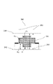
図1は本発明の実施例1の面発光レーザ200の断面模式図である。
面発光レーザ200は、基板210上に、下部ミラー212、活性層214、上部216が積層されている積層構造体を有する。
FIG. 1 is a schematic sectional view of a
The
基板210は、例えばn型にドープされたGaAsである。
下部ミラー212は、例えば光学厚さλ/4ずつ70ペア積層されたn型のAl0.5Ga0.5As/Al0.9Ga0.1Asからなる多層膜反射鏡である。
活性層214は、例えばGaInP/AlGaInPからなる多重量子井戸構造であり、電流注入によりレーザ発振波長λ=680nmにおいて光学利得を持つ。
The
The
The
上部ミラー216は、例えば光学厚さλ/4ずつ35ペア積層されたp型のAl0.5Ga0.5As/Al0.9Ga0.1Asである。
活性層214および上部ミラー216をエッチングすることにより、例えば直径30μmの円筒状のメサ構造が形成されている。
上部ミラー216の一部には、例えば30nmのAl0.98Ga0.02Asからなる層があり、メサ構造の側壁から一部が酸化されて酸化領域を形成している。酸化領域は絶縁体となり、非酸化領域と比べて屈折率が低下している。
この酸化領域と未酸化領域により活性層214に流れる電流の空間分布を制限する電流狭窄構造218が形成されている。なお、未酸化領域は、例えば直径5μmの円形状である。
The
By etching the
A part of the
The oxidized region and the unoxidized region form a current confinement structure 218 that limits the spatial distribution of current flowing in the
上部ミラー216の上には、光学厚さが面内で異なる表面段差構造270が形成されている。ここで、上部216と表面段差構造270との境界を上側境界面242とする。
On the
表面段差構造270(第1の表面段差構造)は第1の構造体280からなる。
第1の構造体280は屈折率n1の第1の材料からなる。例えば、第1の材料はp型のAlGaAsでありn1=3.3である。また、環境媒質240は屈折率n0(<n1)の媒質であり、n0=1の空気である。
基板210の下には、例えばAuGe/Auからなる下部電極220が形成されている。また、第1の構造体280上には、例えばTi/Pt/Auからなる上部電極222が形成されている。
The surface step structure 270 (first surface step structure) includes a
The
A
第1の構造体280は、光出射領域内の中央部に位置する第1の領域260において実厚さがd11であり、第1の領域260より外側に位置する第2の領域262において実厚さがd12である。
The
第1の領域260とは、電流狭窄構造218の未酸化領域と中心をほぼ同じくする円形領域である。例えば、面発光レーザの上部から見たときに、第1の領域は前記未酸化領域の内側にある直径4μmの円形領域である。
The
第2の領域262とは、第1の領域260を取り囲む領域である。
The
本実施例では、第1の構造体280の断面は凹型となっており、d11<d12である。
In the present embodiment, the
第1の構造体280の光学厚さは、第1の領域においてλ/4の偶数倍、第2の領域においてλ/4の奇数倍となっている。すなわち、|n1(d11−d12)|=λ/4×(2M−1)という条件を満たしている(Mは整数)。
The optical thickness of the
例えば、d11=(λ/n1)×(1/2)、d12=(λ/n1)×(7/4)であるときに、|n1(d11−d12)|=|1/2−7/4|=5/4となる。この場合、M=3であり、上記条件を満たす。 For example, when d 11 = (λ / n 1 ) × (1/2) and d 12 = (λ / n 1 ) × (7/4), | n 1 (d 11 −d 12 ) | = | 1 / 2−7 / 4 | = 5/4. In this case, M = 3, which satisfies the above condition.
この結果、波長λの光における活性層214側からみた上部ミラー216および表面段差構造270による反射率を領域ごとに変化させることができる。例えば、第1の領域260の反射率を第2の領域262の反射率よりも高くすることができる。これにより、面発光レーザ200では高次の横モードの発振が抑制され、基本横モードのみが発振する単一横モード発振を実現できる。
As a result, the reflectance by the
一方、波長λの光における活性層214側からみた上部ミラー216および表面段差構造270の透過係数の振幅は、第1の領域260の透過係数の振幅よりも、第2の領域262の透過係数の振幅の方が高くなっている。その比は例えば3倍である。
On the other hand, the amplitude of the transmission coefficient of the
また、表面段差構造270の光学厚さが面内で異なることから、上記透過係数には第1の領域260と第2の領域262とで位相差がある。
表面段差構造270の上部に位置している基板210に平行な面を第1の平面244とする。
In addition, since the optical thickness of the
A plane parallel to the
第1の領域260、第2の領域262における上部境界面242と第1の平面244との光学距離をそれぞれL1、L2とすると、光路長の差はL2−L1で与えられる。L2−L1=(d12−d11)×(n1−n0)=(d12 ×n1−d11 ×n1)×(1−n0/n1)である。
上記数値を代入すると、L2−L1=(7λ/4−λ/2)×(1−1/3.3)=0.871λであり、Nは1となる。
When the optical distances between the
When the above numerical values are substituted, L 2 −L 1 = (7λ / 4−λ / 2) × (1-1 / 3.3) = 0.871λ, and N is 1.
また、この光路長差により出射光に与えられる位相差の大きさは|L2−L1−Nλ|・2π/λで与えられる。Nは上記の値を最小にする整数である。
N=1の場合、|L2−L1−Nλ|・2π/λ=0.258πとなる。
Further, the magnitude of the phase difference given to the outgoing light by this optical path length difference is given by | L 2 −L 1 −Nλ | · 2π / λ. N is an integer that minimizes the above value.
When N = 1, | L 2 −L 1 −Nλ | · 2π / λ = 0.258π.
本実施例と同じ反射率分布で第1の構造体の実厚さの差を最小とする構成、すなわちd11=(λ/n1)×(1/2)、d12=(λ/n1)×(3/4)とした場合を比較例とする。
比較例ではL2−L1=(λ/4)×(1−n0/n1)=0.174λである。
ここで|L2−L1−Nλ|を最小にする整数Nは、0となる。
N=0の場合、|L2−L1−Nλ|・2π/λ=0.348πとなる。
A configuration in which the difference in actual thickness of the first structure is minimized with the same reflectance distribution as in this embodiment, that is, d 11 = (λ / n 1 ) × (1/2), d 12 = (λ / n) 1 ) × (3/4) is a comparative example.
In the comparative example, L 2 −L 1 = (λ / 4) × (1−n 0 / n 1 ) = 0.174λ.
Here, the integer N that minimizes | L 2 −L 1 −Nλ | is 0.
In the case of N = 0, | L 2 −L 1 −Nλ | · 2π / λ = 0.348π.
すなわち、本実施例は比較例に比べて、表面段差構造による位相差を抑えられており、FFPの位相分布を一定に近づけることができる。 That is, in this embodiment, compared with the comparative example, the phase difference due to the surface step structure is suppressed, and the phase distribution of the FFP can be made closer to a constant value.
以上のように、本実施例は、光路長L1と光路長L2について、|L2−L1−Nλ|を最小にする整数Nに対し、以下の式を満たす。
|L2−L1−Nλ|<(λ/4)×(1−n0/n1)
また、|L2−L1−Nλ|=0を満たすことがより好ましい。
As described above, the present embodiment satisfies the following expression with respect to the integer N that minimizes | L 2 −L 1 −Nλ | for the optical path length L 1 and the optical path length L 2 .
| L 2 −L 1 −Nλ | <(λ / 4) × (1−n 0 / n 1 )
Further, it is more preferable to satisfy | L 2 −L 1 −Nλ | = 0.
以上のように、本発明の実施例は、|L2−L1−Nλ|・2π/λの値を小さくすることを目的としているため、L2−L1は所望の反射率分布が得られる値の中で必ずしも最小値とはならない。 As described above, since the embodiment of the present invention aims to reduce the value of | L 2 −L 1 −Nλ | · 2π / λ, L 2 −L 1 has a desired reflectance distribution. It is not necessarily the minimum value that can be obtained.
なお、|N|の値は、小さければ小さいほど、表面段差構造の膜厚を薄くすることができるため、|N|=2よりも|N|=1の方が好ましい。また、より好ましくは、N=0である。
なお、上記実施例ではd11<d12である凹型の表面段差構造を説明したが、d11>d12である凸型の表面段差構造としてもよい。
Note that | N | = 1 is more preferable than | N | = 2 because the smaller the value of | N |, the thinner the thickness of the surface step structure. More preferably, N = 0.
In the above embodiment <has been described a concave surface step structure is d 12, d 11> d 11 may be the stepped structure of the convex is a d 12.
図2に、凸型の表面段差構造の断面図を示す。図2において、上部ミラーの上部境界面242より下側は省略している。
例えば、d11=(λ/n1)×(3/2)、d12=(λ/n1)×(1/4)であり、上部ミラーおよび表面段差構造による反射率は第1の領域に比べて第2の領域で低くなっている。
FIG. 2 shows a cross-sectional view of a convex surface step structure. In FIG. 2, the lower side of the
For example, d 11 = (λ / n 1 ) × (3/2), d 12 = (λ / n 1 ) × (1/4), and the reflectance by the upper mirror and the surface step structure is the first region. Is lower in the second region.
この場合、L2−L1=−0.871λであり、N=−1となり、|L2−L1−Nλ|・2π/λ=0.258πとなる。したがって、比較例に比べて表面段差構造による位相差を抑えられている。 In this case, L 2 −L 1 = −0.871λ, N = −1, and | L 2 −L 1 −Nλ | · 2π / λ = 0.258π. Therefore, the phase difference due to the surface step structure is suppressed as compared with the comparative example.
本発明における面発光レーザのFFPの計算例を図3に示す。
図3(A)はFFP強度分布を角度0°の値で規格化して表示したものである。
図3(B)はFFPの位相を2πで除した値の分布について、それぞれ角度0°の値を0として表示したものである。
面発光レーザの基本横モードは、有効屈折率近似を用いて、コア直径5μm、円形のコア屈折率3.3、コア・クラッド間の比屈折率差が0.3%のLP01モードで与えられるとする。
A calculation example of the FFP of the surface emitting laser in the present invention is shown in FIG.
FIG. 3A shows the FFP intensity distribution normalized by a value of an angle of 0 °.
FIG. 3B shows the distribution of values obtained by dividing the FFP phase by 2π, with the value at an angle of 0 ° being set to zero.
The fundamental transverse mode of the surface emitting laser is given by the LP01 mode using an effective refractive index approximation, with a core diameter of 5 μm, a circular core refractive index of 3.3, and a relative refractive index difference between the core and the cladding of 0.3%. And
図3(A)および(B)の(a)は、表面段差構造がないときのFFPの強度分布および位相分布である。また、図3(A)および(B)の(b)から(d)は、表面段差構造があるときのFFPの強度分布および位相分布である。 3A and 3B show the FFP intensity distribution and phase distribution when there is no surface step structure. 3A and 3B, (b) to (d) are the FFP intensity distribution and phase distribution when there is a surface step structure.
ここで、表面段差構造は、発光中央に位置する直径4μmの円形の第1の領域と、それを取り囲む第2の領域において、透過係数の振幅比が1:3であるとしている。また、透過係数の位相差は、(b)がπ/3、(c)がπ/6、(d)が0である。なお、FFPの計算においてはスカラー回折理論による近似を用いている。 Here, in the surface step structure, the amplitude ratio of the transmission coefficient is 1: 3 in the circular first region having a diameter of 4 μm located at the light emission center and the second region surrounding the first region. The phase difference of the transmission coefficient is π / 3 for (b), π / 6 for (c), and 0 for (d). In the calculation of FFP, approximation based on scalar diffraction theory is used.
図3(B)により、(b)では角度によって位相が大きく異なっていたのが、(c)や(d)では、位相分布の変化を抑制することが可能となっている。すなわち、透過係数の位相差を0に近づけていくにつれて、FFPの角度0近傍での位相分布の変化を抑制でき、FFPの波面収差を抑制することができる。 In FIG. 3B, the phase is greatly different depending on the angle in FIG. 3B, but in FIG. 3C and FIG. 3D, it is possible to suppress the change in the phase distribution. That is, as the phase difference of the transmission coefficient is brought closer to 0, the change in the phase distribution near the FFP angle of 0 can be suppressed, and the wavefront aberration of the FFP can be suppressed.
図4に実施例2にかかる面発光レーザの断面模式図を示す。 FIG. 4 is a schematic sectional view of a surface emitting laser according to Example 2.
実施例2の面発光レーザは、上部ミラー216の上に表面段差構造272が形成されている点で実施例1と同じである。
The surface emitting laser according to the second embodiment is the same as the first embodiment in that a
実施例2の面発光レーザにおける表面段差構造272は、第1の構造体280と、第2の構造体282からなることが特徴である。
The
表面段差構造に複数の構造体を用いることで、反射率分布を持つ上部ミラーおよび表面段差構造の透過係数の位相差をより抑えることができる。 By using a plurality of structures for the surface step structure, it is possible to further suppress the phase difference between the transmission coefficients of the upper mirror having the reflectance distribution and the surface step structure.
第1の構造体280は屈折率n1の第1の材料からなり、第2の構造体282は屈折率n2(<n1)の第2の材料からなる。
上部電極222は、例えば第1の構造体280の上部に配されている。
第1の材料は例えばAlGaAsであり、n1=3.3である。
第2の材料は例えばSiO2であり、n2=1.5である。
図4に示すように、第1の領域260および第2の領域262における第1の構造体280の実厚さをそれぞれd11、d12とする。
The
The
The first material is AlGaAs, for example, and n 1 = 3.3.
The second material is, for example, SiO 2 and n 2 = 1.5.
As shown in FIG. 4, the actual thicknesses of the
また、図4に示すように、第1の領域260および第2の領域262における第2の構造体282の実厚さをそれぞれd21、d22とする。
ここでは、図4に示すように、d11<d12、および、d21<d22であるとする。
第1の構造体280の光学厚さは第1の領域においてλ/4の偶数倍、第2の領域においてλ/4の奇数倍となっている。
例えば、d11=(λ/n1)×(1/2)、d12=(λ/n1)×(3/4)である。
Further, as shown in FIG. 4, the actual thicknesses of the
Here, as shown in FIG. 4, it is assumed that d 11 <d 12 and d 21 <d 22 .
The optical thickness of the
For example, d 11 = (λ / n 1 ) × (1/2) and d 12 = (λ / n 1 ) × (3/4).
これにより、第1の構造体280と第2の構造体282の界面の位置が第1の領域と第2の領域とで異なり、上部ミラーおよび表面段差構造による反射率を第1の領域に比べて第2の領域で低くすることができる。
As a result, the position of the interface between the
次に、表面段差構造による透過係数の位相差が0(2πの整数倍)に近づくように、第2の構造体282の実厚さを設定する。
好ましくは、表面段差構造による透過係数の位相差が0(2πの整数倍)となるように第2の構造体282の実厚さを設定する。
実施例1と同様に、第1の領域260、第2の領域262における上部境界面242と第1の平面244との光学距離をそれぞれL1、L2とする。
表面段差構造による位相差の大きさは|L2−L1−Nλ|・2π/λで与えられる。ここでNは上記の値を最小にする整数である。
L2−L1
=(d12−d11)(n1−n0)+(d22−d21)(n2−n0)
=(d12 ×n1−d11 ×n1)(1−n0/n1)+(d22 ×n2−d21 ×n2)(1−n0/n2)である。
なお、第2の構造体282の光学厚さがλ/4の偶数倍であれば、第2の構造体282によって上部ミラー216および表面段差構造272による反射率は変化しない。
Next, the actual thickness of the
Preferably, the actual thickness of the
As in the first embodiment, the optical distances between the
The magnitude of the phase difference due to the surface step structure is given by | L 2 −L 1 −Nλ | · 2π / λ. Here, N is an integer that minimizes the above value.
L 2 -L 1
= (D 12 -d 11) ( n 1 -n 0) + (d 22 -d 21) (n 2 -n 0)
A = (d 12 × n 1 -d 11 × n 1) (1-
Note that if the optical thickness of the
例えば、d21=(λ/n2)×(1/2)、d22=(λ/n2)×3とすると、L2−L1=1.01λとなる。この場合、N=1となり、|L2−L1−Nλ|=0.01λとなり、位相差|L2−L1−Nλ|・2π/λ=0.02πとすることができる。 For example, when d 21 = (λ / n 2 ) × (½) and d 22 = (λ / n 2 ) × 3, L 2 −L 1 = 1.01λ. In this case, N = 1, | L 2 −L 1 −Nλ | = 0.01λ, and the phase difference | L 2 −L 1 −Nλ | · 2π / λ = 0.02π.
また、高反射率領域である第1の領域においては、第2の構造体の光学厚さがλ/4の偶数倍からずれても反射率はあまり変化しない。例えば、d21=(λ/n2)×0.52、d22=(λ/n2)×3とすると、L2−L1=λとなる。この場合、N=1となり、位相差|L2−L1−Nλ|・2π/λ=0とすることができる。 Further, in the first region, which is a high reflectance region, the reflectance does not change much even if the optical thickness of the second structure is deviated from an even multiple of λ / 4. For example, if d 21 = (λ / n 2 ) × 0.52 and d 22 = (λ / n 2 ) × 3, then L 2 −L 1 = λ. In this case, N = 1 and the phase difference | L 2 −L 1 −Nλ | · 2π / λ = 0.
上記実施例においては、d11<d12、および、d21<d22である第1の構造体280および第2の構造体282が凹型である表面段差構造について説明した。しかし、図5に示すように、d11>d12、および、d21>d22である第1の構造体280および第2の構造体282が凸型である表面段差構造としてもよい。
例えば、n0=1、n1=3.3、n2=1.5であるとき、
d11=(λ/n1)×(1/2)、
d12=(λ/n1)×(1/4)、
d21=(λ/n2)×3、
d22=(λ/n2)×(1/2)とすれば、
L2−L1=−1.01λとなり、N=−1として、表面段差構造による位相差の大きさを0.02πとすることができる。また、
d21=(λ/n2)×2.98、
d22=(λ/n2)×(1/2)とすれば、
L2−L1=−λとなり、N=−1として、表面段差構造による位相差の大きさを0とすることができる。
In the above embodiment, the surface step structure in which the
For example, when n 0 = 1, n 1 = 3.3, and n 2 = 1.5,
d 11 = (λ / n 1 ) × (1/2),
d 12 = (λ / n 1 ) × (1/4),
d 21 = (λ / n 2 ) × 3,
If d 22 = (λ / n 2 ) × (1/2),
Since L 2 −L 1 = −1.01λ and N = −1, the magnitude of the phase difference due to the surface step structure can be set to 0.02π. Also,
d 21 = (λ / n 2 ) × 2.98,
If d 22 = (λ / n 2 ) × (1/2),
Since L 2 −L 1 = −λ and N = −1, the magnitude of the phase difference due to the surface step structure can be set to zero.
また、図6に示すように、d11<d12、および、d21>d22とすることもできる。すなわち、第1の構造体280が凹型であり、第2の構造体282が凸型である表面段差構造を設けてもよい。
例えば、n0=1、n1=3.3、n2=1.5であるとき、
d11=(λ/n1)×(1/2)、
d12=(λ/n1)×(3/4)、
d21=(λ/n2)、
d22=(λ/n2)×(1/2)とすれば、
L2−L1=0.01λとなり、N=0として、表面段差構造による位相差の大きさを0.02πとすることができる。また、
d21=(λ/n2)×1.02、
d22=(λ/n2)×(1/2)とすれば、
L2−L1=0となり、N=0として、表面段差構造による位相差の大きさを0とすることができる。また、図7に示すように、d11>d12、および、d21<d22とすることもできる。すなわち、第1の構造体280が凸型であり、第2の構造体282が凹型である表面段差構造を設けてもよい。
Further, as shown in FIG. 6, d 11 <d 12 and d 21 > d 22 may be satisfied. That is, a surface step structure in which the
For example, when n 0 = 1, n 1 = 3.3, and n 2 = 1.5,
d 11 = (λ / n 1 ) × (1/2),
d 12 = (λ / n 1 ) × (3/4),
d 21 = (λ / n 2 ),
If d 22 = (λ / n 2 ) × (1/2),
When L 2 −L 1 = 0.01λ and N = 0, the phase difference due to the surface step structure can be set to 0.02π. Also,
d 21 = (λ / n 2 ) × 1.02,
If d 22 = (λ / n 2 ) × (1/2),
Since L 2 −L 1 = 0 and N = 0, the magnitude of the phase difference due to the surface step structure can be set to zero. Further, as shown in FIG. 7, d 11> d 12, and may be a d 21 <d 22. That is, a surface step structure in which the
例えば、n0=1、n1=3.3、n2=1.5であるとき、
d11=(λ/n1)×(1/2)、
d12=(λ/n1)×(1/4)、
d21=(λ/n2)×(1/2)、
d22=(λ/n2)とすれば、
L2−L1=−0.01λとなり、N=0として、表面段差構造による位相差の大きさを0.02πとすることができる。また、
d21=(λ/n2)×0.48、
d22=(λ/n2)とすれば、
L2−L1=0となり、N=0として、表面段差構造による位相差の大きさを0とすることができる。
For example, when n 0 = 1, n 1 = 3.3, and n 2 = 1.5,
d 11 = (λ / n 1 ) × (1/2),
d 12 = (λ / n 1 ) × (1/4),
d 21 = (λ / n 2 ) × (1/2),
If d 22 = (λ / n 2 ),
L 2 −L 1 = −0.01λ, and N = 0, the phase difference due to the surface step structure can be set to 0.02π. Also,
d 21 = (λ / n 2 ) × 0.48,
If d 22 = (λ / n 2 ),
Since L 2 −L 1 = 0 and N = 0, the magnitude of the phase difference due to the surface step structure can be set to zero.
図6、図7に示す構造、すなわち(d11−d12)×(d21−d22)<0の場合は、N=0とできるため、(d11−d12)×(d21−d22)>0の場合よりも表面段差構造の厚さを抑えることが可能である。これにより、作成精度の向上や、段差構造の第1領域および第2の領域の境界部での光散乱の抑制という利点が得られる。
なお、d11、d12、d21、d22はすべて正の値である必要はなく、本発明の主旨の範囲で一つまたは二つが0であっても良い。
In the case of the structure shown in FIGS. 6 and 7, that is, (d 11 −d 12 ) × (d 21 −d 22 ) <0, N = 0 can be established, so (d 11 −d 12 ) × (d 21 − It is possible to suppress the thickness of the surface step structure as compared with the case of d 22 )> 0. As a result, there are obtained advantages such as improvement in production accuracy and suppression of light scattering at the boundary between the first region and the second region of the step structure.
Note that d 11 , d 12 , d 21 , and d 22 need not all be positive values, and one or two of them may be 0 within the scope of the present invention.
図8に実施例3にかかる面発光レーザの断面模式図を示す。
実施例3の面発光レーザにおける表面段差構造272は、実施例2と同様、第1の構造体280と第2の構造体282からなることが特徴である。
実施例3の面発光レーザにおいては、実施例2と異なり、第1の構造体280は屈折率n1の第1の材料からなり、第2の構造体282は屈折率n2(>n1)の第2の材料からなる。
第1の材料は例えばSiO2であり、n1=1.5である。
第2の材料は例えばSiNであり、n 2 =2.0である。
上部電極222は、例えば上部ミラー216の上部に配されている。
n1<n2、かつ、n2>n0であるから、d11をλ/4の奇数倍、d21をλ/4の奇数倍とすることで、第1の領域260における上部ミラー216および表面段差構造272による反射率を高めることができる。
FIG. 8 is a schematic sectional view of a surface emitting laser according to Example 3.
The
In the surface emitting laser of Example 3, unlike Example 2, the
The first material is, for example, SiO 2 and n 1 = 1.5.
The second material is, for example, SiN, and n 2 = 2.0.
The
Since n 1 <n 2 and n 2 > n 0 , the
また、d12をλ/4の偶数倍、d22をλ/4の奇数倍とすることで、第2の領域262における上部ミラーおよび表面段差構造による反射率を下げることができる。
d11<d12でも良いし、d11>d12でも良い。
また、d21<d22でも良いし、d21>d22でも良い。
簡単のため、d12=0とし、参照構造をd11=d21=d22=λ/4とすると、L2−L1=−0.083λとなり、N=0として、表面段差構造による位相差の大きさは0.166πとなる。
これに対し、本実施例において、例えばd11=0.75、d21=1.75、d22=0.25とすることで、L2−L1=−λとなり、N=−1として、表面段差構造による位相差の大きさを0とすることができる。
Further, even multiple of the d 12 lambda / 4, by an odd multiple of the d 22 lambda / 4, it is possible to reduce the reflectance by the top mirror and the stepped structure in the
<to even d 12 good, d 11> d 11 d 12 even good.
Further, d 21 <d 22 may be satisfied, or d 21 > d 22 may be satisfied.
For simplicity, if d 12 = 0 and the reference structure is d 11 = d 21 = d 22 = λ / 4, then L 2 −L 1 = −0.083λ, and N = 0, The magnitude of the phase difference is 0.166π.
On the other hand, in the present embodiment, for example, by setting d 11 = 0.75, d 21 = 1.75, and d 22 = 0.25, L 2 −L 1 = −λ and N = −1. The magnitude of the phase difference due to the surface step structure can be made zero.
また、d11=0.75、d21=0.25、d22=0.75とすることで、L2−L1=0となり、N=0として、表面段差構造による位相差の大きさを0とすることができる。 Further, by setting d 11 = 0.75, d 21 = 0.25, and d 22 = 0.75, L 2 −L 1 = 0 and N = 0, and the magnitude of the phase difference due to the surface step structure Can be set to zero.
(製造方法)
本実施例の面発光レーザの製造方法の一例を示す。
基板210は例えばn型のGaAs基板である。
基板210上に、例えばMOCVD法により、下部ミラー212、活性層214、上部ミラー216を成膜する。
(Production method)
An example of the manufacturing method of the surface emitting laser of a present Example is shown.
The
A
下部ミラー212は光学厚さλ/4ずつ70ペア積層されたn型のAl0.5Ga0.5As/Al0.9Ga0.1Asからなる多層膜反射鏡である。
活性層214はGaInP/AlGaInPからなる多重量子井戸構造であり、電流注入によりレーザ発振波長λ=680nmにおいて光学利得を持つ。
上部ミラー216は光学厚さλ/4ずつ35ペア積層されたp型のAl0.5Ga0.5As/Al0.9Ga0.1Asである。
上部ミラー216の一部に実厚さ30nmのAl0.98Ga0.02Asからなる酸化可能層が含まれる。
The
The
The
A part of the
また、表面段差構造の第1の構造体280として半導体を用いる場合、上部ミラー216に引き続き成膜しても良い。
In the case where a semiconductor is used as the
次に、例えばドライエッチングにて、活性層214および上部ミラー216をエッチングし、例えば直径30μmの円筒状のメサ構造を形成する。
第1の構造体280が成膜されている場合は第1の構造体280もエッチングする。
Next, the
In the case where the
メサ構造の側壁から、前記酸化可能層を酸化する。酸化は例えば水蒸気雰囲気にて450℃に加熱し30分間行う。これにより、酸化可能層に、酸化領域と未酸化領域とからなる電流狭窄構造218を形成する。
未酸化領域はメサ構造と中心を同じくする、直径5μmの円形状である。
The oxidizable layer is oxidized from the side wall of the mesa structure. The oxidation is performed, for example, by heating to 450 ° C. in a steam atmosphere for 30 minutes. As a result, a current confinement structure 218 composed of an oxidized region and an unoxidized region is formed in the oxidizable layer.
The unoxidized region has a circular shape having a diameter of 5 μm and the same center as the mesa structure.
この後、メサ側壁を絶縁膜などで保護する。 Thereafter, the mesa side wall is protected with an insulating film or the like.
基板210下にAuGe/Auからなる下部電極220を形成する。また、上部ミラー270または第1の構造体280上にTi/Pt/Auからなる上部電極222を形成する。
A
上記面発光レーザの作製工程において、上部ミラー216または第1の構造体280の成膜工程以後のどこかで、表面段差構造272を形成する。
In the surface emitting laser manufacturing process, the
例えば電流狭窄構造218の形成工程後に表面段差構造272を形成する。
表面段差構造272はエッチングなどにより形成することができる。
For example, the
The
図4や図5に示す構造のように、(d11−d12)×(d21−d22)>0である表面段差構造の形成方法について、図4の構造を図9を用いて説明する。 4A and 4B, a method of forming a surface step structure in which (d 11 −d 12 ) × (d 21 −d 22 )> 0 as in the structure shown in FIGS. 4 and 5 will be described with reference to FIG. To do.
図9(a)に示すように、上部ミラー216上に、第1の層300を形成し、その上に第2の層302を形成する。
第1の層300は、例えば半導体層であり、AlGaAsである。あるいは、第1の層300は、例えば誘電体層であり、SiO2である。
第2の層302は、例えば誘電体層であり、SiNである。
第1の層300、第2の層302は例えばMOCVD法、プラズマCVD法やスパッタ法により形成する。
As shown in FIG. 9A, the
The
The
The
第2の層302上にレジスト320を塗布し、フォトリソグラフィにより第2の領域262のレジスト320を除去しパターンを形成する。
次に、図9(b)に示すように、レジスト320をマスクとして、第2の層302および第1の層300をエッチングする。
エッチングは例えばリン酸やバッファードフッ酸によるウエットエッチングにより行う。
A resist 320 is applied over the
Next, as shown in FIG. 9B, the
Etching is performed, for example, by wet etching using phosphoric acid or buffered hydrofluoric acid.
次に、図9(c)に示すように、例えば有機溶剤にてレジスト320を除去する。
次に、図9(d)に示すように、第1の層300および第2の層302の上部に、第3の層304を例えばプラズマCVD法やスパッタ法により成膜する。
第3の層304は、第2の層302と屈折率が近い、または屈折率が同じ材料である。
Next, as shown in FIG. 9C, the resist 320 is removed with, for example, an organic solvent.
Next, as shown in FIG. 9D, a
The
このようにして、第1の層300からなる第1の構造体280、および、第2の層302と第3の層304からなる第2の構造体282が形成される。
同様の手順で、レジスト320の除去位置を第1の領域260とすることで、図4に示す表面段差構造を形成することも可能である。
In this manner, the
The surface step structure shown in FIG. 4 can be formed by setting the removal position of the resist 320 to the
次に、図6や図7に示す構造のように、(d11−d12)×(d21−d22)<0である表面段差構造の形成方法について、図7の構造を図10を用いて説明する。 Next, as shown in FIG. 6 and FIG. 7, a method for forming a surface step structure in which (d 11 −d 12 ) × (d 21 −d 22 ) <0 will be described with reference to FIG. It explains using.
図10(a)に示すように、上部ミラー216上に、第1の層300を形成する。第1の層300は半導体または誘電体である。第1の層は例えばMOCVD法、プラズマCVD法やスパッタ法により形成する。
As shown in FIG. 10A, the
第1の層300上にレジスト320を塗布し、フォトリソグラフィにより第2の領域262のレジスト320を除去しパターンを形成する。このとき、残るレジスト形状はレジスト上部よりも下部のほうが断面積が狭い逆テーパー状となっていることが好ましい。
A resist 320 is applied on the
次に、図10(b)に示すように、レジスト320をマスクとして、第1の層300をエッチングする。エッチングは例えばリン酸やバッファードフッ酸によるウエットエッチングにより行う。
次に、図10(c)に示すように、第1の層300およびレジスト320の上部に、第2の層302を例えばスパッタ法により成膜する。
次に、図10(d)に示すように、例えば有機溶剤にてレジスト320を除去する。このとき、レジスト320上に形成されていた第2の層302も同時に除去される。
次に、図10(e)に示すように、第1の層300および第2の層302の上部に、第3の層304を例えばプラズマCVD法やスパッタ法により成膜する。
第3の層304は、第2の層302と屈折率が近い、または屈折率が同じ材料である。
Next, as shown in FIG. 10B, the
Next, as shown in FIG. 10C, the
Next, as shown in FIG. 10D, the resist 320 is removed with, for example, an organic solvent. At this time, the
Next, as shown in FIG. 10E, a
The
このようにして、第1の層300からなる第1の構造体280、および、第2の層302と第3の層304からなる第2の構造体282が形成される。
同様の手順で、レジスト320の除去位置を第1の領域260とすることで、図6に示す表面段差構造を形成することも可能である。
In this manner, the
The surface step structure shown in FIG. 6 can be formed by setting the removal position of the resist 320 to the
実施例1乃至3で説明した面発光レーザを複数配して構成された面発光レーザアレイ光源と走査装置を用いた応用例として、電子写真方式の画像形成装置について説明する。 An electrophotographic image forming apparatus will be described as an application example using a surface emitting laser array light source configured by arranging a plurality of surface emitting lasers described in the first to third embodiments and a scanning device.
図11(a)は画像形成装置の平面図であり、図11(b)は同装置の側面図である。図11において、500は感光ドラム、502は帯電器、504は現像器、506は転写帯電器、508は定着器、510は回転多面鏡、512はモータである。また、514は面発光レーザアレイ光源、516は反射鏡、520はコリメータレンズ、521はシリンドリカルレンズ、及び522はf−θレンズである。モータ512は回転多面鏡510を回転駆動するものである。
FIG. 11A is a plan view of the image forming apparatus, and FIG. 11B is a side view of the apparatus. In FIG. 11, 500 is a photosensitive drum, 502 is a charger, 504 is a developing device, 506 is a transfer charger, 508 is a fixing device, 510 is a rotary polygon mirror, and 512 is a motor. Also, 514 is a surface emitting laser array light source, 516 is a reflecting mirror, 520 is a collimator lens, 521 is a cylindrical lens, and 522 is an f-θ lens. The
コリメータレンズ520と回転多面鏡510の間の光軸上には主走査開口絞り530が置かれている。レーザアレイ光源514とシリンドリカルレンズ521の間に副走査開口絞り532が置かれている。
A main
面発光レーザアレイ光源514は直線偏光であり、その方向は例えば主走査方向に平行であるとする。
The surface emitting laser array
図11において、本実施形態における回転多面鏡510は、例えば6つの反射面を備えている。面発光レーザアレイ514は、記録用光源となるものであり、ドライバにより画像信号に応じて点灯または消灯するように構成されている。こうして光変調されたレーザ光は、面発光レーザアレイ514からの光を集光するコリメータレンズ520を介し回転多面鏡510に向けて照射される。
In FIG. 11, the
回転多面鏡510は矢印方向に回転していて、面発光レーザアレイ514から出力されたレーザ光は、回転多面鏡510の回転に伴い、その反射面で連続的に出射角度を変える偏向ビームとして反射される。この反射光は、f−θレンズ522により歪曲収差の補正等を受け、反射鏡516を経て感光ドラム500に照射され、感光ドラム500上で主走査方向に走査される。このとき、回転多面鏡510の1面を介したビーム光の反射により、感光ドラム500の主走査方向に面発光レーザアレイ514に対応した複数のライン分の画像が形成される。
The
感光ドラム500は、予め帯電器502により帯電されており、レーザ光の走査により順次露光され、静電潜像が形成される。また、感光ドラム500は矢印方向に回転していて、形成された静電潜像は、現像器504により現像され、現像された可視像は転写帯電器506により、転写紙に転写される。可視像が転写された転写紙は、定着器508に搬送され、定着を行った後に機外に排出される。
The
(その他の実施形態)
本発明は上記形態に制限されるものではなく、様々な変更及び変形が可能である。例えば、第1の構造体を構成する第1の材料は、環境媒質や第2の材料との屈折率との差が大きければ、お互いに屈折率の近い複数の材料で構成されていてもよい。例えば、第2の構造体を構成する第2の材料は、環境媒質や第1の材料との屈折率との差が大きければ、お互いに屈折率の近い複数の材料で構成されていてもよい。
(Other embodiments)
The present invention is not limited to the above embodiment, and various changes and modifications can be made. For example, the first material constituting the first structure may be composed of a plurality of materials having a refractive index close to each other as long as the difference between the refractive index and the environmental medium or the second material is large. . For example, the second material constituting the second structure may be composed of a plurality of materials having a refractive index close to each other as long as the difference between the refractive index of the environmental medium and the first material is large. .
200 面発光レーザ
210 基板
212 下部ミラー
214 活性層
216 上部ミラー
218 電流狭窄構造
220 下部電極
222 上部電極
240 環境媒質
242 上部境界面
244 第1の平面
260 第1の領域
262 第2の領域
270 表面段差構造
280 第1の構造体
282 第2の構造体
300 第1の層
302 第2の層
304 第3の層
320 レジスト
200
Claims (11)
前記上部ミラーの上部に設けられ、光出射領域内の中央部に位置する第1の領域と、該光出射領域内であって、該第1の領域より外側に位置する第2の領域との間に段差を有する表面段差構造を備え、
前記表面段差構造は環境媒質の屈折率n0よりも大きい屈折率n1の第1の材料からなる第1の構造体を含み、
前記第1の構造体の前記第1の領域における実厚さをd11、前記第1の構造体の前記第2の領域における実厚さをd12とすると、|n1(d11−d12)|=λ/4×(2M−1)であり(Mは整数)、
前記表面段差構造の上部に位置している前記基板に平行な面と、前記上部ミラーの上部境界面、との間の光路長に関して、
前記第1の領域における前記光路長L1と、前記第2の領域における前記光路長L2が、|L2−L1−Nλ|を最小にする整数Nに対し、以下の式を満たすことを特徴とする面発光レーザ。
|L2−L1−Nλ|<(λ/4)×(1−n0/n1) On a substrate, a lower mirror having an active layer, a laminated structure comprising an upper mirror, and a surface emitting laser that oscillates at a wavelength lambda,
A first region provided at an upper portion of the upper mirror and located at a central portion in the light emitting region; and a second region located outside the first region in the light emitting region. includes a front surface step structure that having a step between,
The surface step structure includes a first structure made of a first material having a refractive index n 1 larger than the refractive index n 0 of the environmental medium,
If the actual thickness of the first region of the first structure d 11, the actual thickness of the second region of the first structure and d 12, | n 1 (d 11 -d 12 ) | = λ / 4 × (2M−1) (M is an integer),
And a plane parallel to said substrate which is positioned above the front Symbol table surface step structure, the upper boundary surface of the upper mirror, with respect to the optical path length between the,
And the optical path length L 1 in the first region, wherein the optical path length L 2 in the second region, | L 2 -L 1 -Nλ | a relative integer N that minimizes, to satisfy the following formula A surface emitting laser characterized by the above.
| L 2 −L 1 −Nλ | <(λ / 4) × (1−n 0 / n 1 )
前記第1の構造体の前記第2の領域における光学厚さはλ/4の奇数倍であることを特徴とする請求項1又は2に記載の面発光レーザ。3. The surface emitting laser according to claim 1, wherein an optical thickness in the second region of the first structure is an odd multiple of λ / 4. 4.
前記第2の構造体は前記第1の構造体の上に配されており、
前記第2の構造体の前記第1の領域における実厚さd21と、前記第2の領域における実厚さd22とは異なる厚さであることを特徴とする請求項1又は2に記載の面発光レーザ。 Before Symbol Table surface step structure is larger than the n 0, look including a second structure comprising a second material of different refractive index n 2 and the n 1,
The second structure is disposed on the first structure;
The actual thickness d 21 in the first region of the second structure, to claim 1 or 2, characterized in that a thickness that is different from the actual thickness d 22 in the second region The surface emitting laser described.
前記第1の構造体の前記第2の領域における光学厚さはλ/4の奇数倍であり、The optical thickness in the second region of the first structure is an odd multiple of λ / 4;
前記第2の構造体の前記第1の領域における光学厚さと前記第2の構造体の前記第2の領域における光学厚さは、ともにλ/4の偶数倍であることを特徴とする請求項7に記載の面発光レーザ。The optical thickness in the first region of the second structure and the optical thickness in the second region of the second structure are both an even multiple of λ / 4. 8. The surface emitting laser according to item 7.
前記第1の構造体の前記第2の領域における光学厚さはλ/4の偶数倍であり、The optical thickness in the second region of the first structure is an even multiple of λ / 4;
前記第2の構造体の前記第1の領域における光学厚さと前記第2の構造体の前記第2の領域における光学厚さは、ともにλ/4の奇数倍であることを特徴とする請求項9に記載の面発光レーザ。The optical thickness in the first region of the second structure and the optical thickness in the second region of the second structure are both odd multiples of λ / 4. 9. The surface emitting laser according to item 9.
前記面発光レーザから射出されるレーザ光により露光される感光ドラムと、を有する画像形成装置。An image forming apparatus having a photosensitive drum exposed by laser light emitted from the surface emitting laser.
Priority Applications (3)
| Application Number | Priority Date | Filing Date | Title |
|---|---|---|---|
| JP2010276170A JP5743520B2 (en) | 2010-12-10 | 2010-12-10 | Surface emitting laser and image forming apparatus |
| US13/311,310 US9046807B2 (en) | 2010-12-10 | 2011-12-05 | Surface emitting laser |
| CN201110409245.6A CN102545039B (en) | 2010-12-10 | 2011-12-09 | Surface emitting laser |
Applications Claiming Priority (1)
| Application Number | Priority Date | Filing Date | Title |
|---|---|---|---|
| JP2010276170A JP5743520B2 (en) | 2010-12-10 | 2010-12-10 | Surface emitting laser and image forming apparatus |
Publications (2)
| Publication Number | Publication Date |
|---|---|
| JP2012124433A JP2012124433A (en) | 2012-06-28 |
| JP5743520B2 true JP5743520B2 (en) | 2015-07-01 |
Family
ID=46199357
Family Applications (1)
| Application Number | Title | Priority Date | Filing Date |
|---|---|---|---|
| JP2010276170A Active JP5743520B2 (en) | 2010-12-10 | 2010-12-10 | Surface emitting laser and image forming apparatus |
Country Status (3)
| Country | Link |
|---|---|
| US (1) | US9046807B2 (en) |
| JP (1) | JP5743520B2 (en) |
| CN (1) | CN102545039B (en) |
Families Citing this family (2)
| Publication number | Priority date | Publication date | Assignee | Title |
|---|---|---|---|---|
| JP6015220B2 (en) * | 2012-08-07 | 2016-10-26 | 富士ゼロックス株式会社 | Surface emitting semiconductor laser, surface emitting semiconductor laser device, optical transmission device, and information processing device |
| CN104078844A (en) * | 2013-03-29 | 2014-10-01 | 新科实业有限公司 | Multimode Vertical Cavity Surface Emitting Laser with Narrow Lasing Angle |
Family Cites Families (16)
| Publication number | Priority date | Publication date | Assignee | Title |
|---|---|---|---|---|
| JP2523826B2 (en) * | 1988-10-07 | 1996-08-14 | 三菱電機株式会社 | Semiconductor laser |
| US5388120A (en) | 1993-09-21 | 1995-02-07 | Motorola, Inc. | VCSEL with unstable resonator |
| JP2001284722A (en) | 2000-03-29 | 2001-10-12 | Seiko Epson Corp | Surface emitting semiconductor laser and method of manufacturing the same |
| US6727520B2 (en) | 2000-12-29 | 2004-04-27 | Honeywell International Inc. | Spatially modulated reflector for an optoelectronic device |
| JP2003115634A (en) * | 2001-08-02 | 2003-04-18 | Furukawa Electric Co Ltd:The | Surface emitting laser element |
| JP4113576B2 (en) * | 2002-05-28 | 2008-07-09 | 株式会社リコー | Surface emitting semiconductor laser, optical transmission module, optical switching device, and optical transmission system |
| JP3838218B2 (en) | 2003-05-19 | 2006-10-25 | ソニー株式会社 | Surface emitting semiconductor laser device and method for manufacturing the same |
| JP2006019470A (en) * | 2004-07-01 | 2006-01-19 | Sony Corp | Surface emitting semiconductor laser and optical module |
| JP2006210429A (en) * | 2005-01-25 | 2006-08-10 | Sony Corp | Surface emitting semiconductor laser |
| JP5376104B2 (en) * | 2005-07-04 | 2013-12-25 | ソニー株式会社 | Surface emitting semiconductor laser |
| KR100827120B1 (en) | 2006-09-15 | 2008-05-06 | 삼성전자주식회사 | Vertical cross-section laser and its manufacturing method |
| JP4639249B2 (en) * | 2008-07-31 | 2011-02-23 | キヤノン株式会社 | Surface emitting laser manufacturing method, surface emitting laser array manufacturing method, surface emitting laser, surface emitting laser array, and optical apparatus including surface emitting laser array |
| JP5279393B2 (en) * | 2008-07-31 | 2013-09-04 | キヤノン株式会社 | Surface emitting laser and method for manufacturing the same, method for manufacturing surface emitting laser array, and optical apparatus including surface emitting laser array |
| JP2010062267A (en) * | 2008-09-02 | 2010-03-18 | Toshiba Corp | Surface emitting device and method for manufacturing the same, and optical transmission module |
| JP5038371B2 (en) | 2008-09-26 | 2012-10-03 | キヤノン株式会社 | Manufacturing method of surface emitting laser |
| JP5434201B2 (en) * | 2009-03-23 | 2014-03-05 | ソニー株式会社 | Semiconductor laser |
-
2010
- 2010-12-10 JP JP2010276170A patent/JP5743520B2/en active Active
-
2011
- 2011-12-05 US US13/311,310 patent/US9046807B2/en active Active
- 2011-12-09 CN CN201110409245.6A patent/CN102545039B/en active Active
Also Published As
| Publication number | Publication date |
|---|---|
| JP2012124433A (en) | 2012-06-28 |
| CN102545039B (en) | 2014-09-03 |
| US20120147918A1 (en) | 2012-06-14 |
| US9046807B2 (en) | 2015-06-02 |
| CN102545039A (en) | 2012-07-04 |
Similar Documents
| Publication | Publication Date | Title |
|---|---|---|
| KR101463704B1 (en) | Surface emitting laser, surface-emitting-laser array, and image forming apparatus | |
| KR101041492B1 (en) | An optical device comprising a method of manufacturing a surface emitting laser, a method of manufacturing a surface emitting laser array, and a surface emitting laser array manufactured by the manufacturing method | |
| JP5274038B2 (en) | Manufacturing method of vertical cavity surface emitting laser and manufacturing method of laser array | |
| US8900902B2 (en) | Process for producing surface-emitting laser and process for producing surface-emitting laser array | |
| JP2011029496A (en) | Surface emitting laser, method for manufacturing the same and image forming apparatus | |
| JP2010040605A (en) | Surface emitting laser and its manufacturing method, surface emitting laser array and surface emitting laser array manufacturing method, and optical equipment with surface emitting laser array | |
| US9042421B2 (en) | Surface emitting laser, surface emitting laser array, and optical apparatus having surface emitting laser array | |
| JP5893246B2 (en) | Surface emitting laser and surface emitting laser array, surface emitting laser manufacturing method, surface emitting laser array manufacturing method, and optical apparatus including surface emitting laser array | |
| JP5279392B2 (en) | Surface emitting laser and method for manufacturing the same, method for manufacturing surface emitting laser array, and optical apparatus including surface emitting laser array | |
| JP5725804B2 (en) | Surface emitting laser and surface emitting laser array, surface emitting laser manufacturing method, surface emitting laser array manufacturing method, and optical apparatus including surface emitting laser array | |
| JP6061541B2 (en) | Surface emitting laser, image forming apparatus | |
| JP5743520B2 (en) | Surface emitting laser and image forming apparatus | |
| JP5717485B2 (en) | Surface emitting laser, surface emitting laser array, and image forming apparatus | |
| JP2013157473A (en) | Surface emitting laser | |
| JP5769459B2 (en) | Manufacturing method of surface emitting laser and manufacturing method of surface emitting laser array | |
| JP2014127511A (en) | Surface emitting laser element and method for manufacturing the same, surface emitting laser array, light scanning device, and image forming apparatus | |
| JP5335861B2 (en) | Manufacturing method of surface emitting laser |
Legal Events
| Date | Code | Title | Description |
|---|---|---|---|
| A621 | Written request for application examination |
Free format text: JAPANESE INTERMEDIATE CODE: A621 Effective date: 20131209 |
|
| A977 | Report on retrieval |
Free format text: JAPANESE INTERMEDIATE CODE: A971007 Effective date: 20140328 |
|
| A131 | Notification of reasons for refusal |
Free format text: JAPANESE INTERMEDIATE CODE: A131 Effective date: 20140415 |
|
| A521 | Written amendment |
Free format text: JAPANESE INTERMEDIATE CODE: A523 Effective date: 20140613 |
|
| A131 | Notification of reasons for refusal |
Free format text: JAPANESE INTERMEDIATE CODE: A131 Effective date: 20141125 |
|
| A521 | Written amendment |
Free format text: JAPANESE INTERMEDIATE CODE: A523 Effective date: 20150126 |
|
| TRDD | Decision of grant or rejection written | ||
| A01 | Written decision to grant a patent or to grant a registration (utility model) |
Free format text: JAPANESE INTERMEDIATE CODE: A01 Effective date: 20150331 |
|
| A61 | First payment of annual fees (during grant procedure) |
Free format text: JAPANESE INTERMEDIATE CODE: A61 Effective date: 20150428 |
|
| R151 | Written notification of patent or utility model registration |
Ref document number: 5743520 Country of ref document: JP Free format text: JAPANESE INTERMEDIATE CODE: R151 |