JP5724932B2 - Laser scanning optical system - Google Patents
Laser scanning optical system Download PDFInfo
- Publication number
- JP5724932B2 JP5724932B2 JP2012086921A JP2012086921A JP5724932B2 JP 5724932 B2 JP5724932 B2 JP 5724932B2 JP 2012086921 A JP2012086921 A JP 2012086921A JP 2012086921 A JP2012086921 A JP 2012086921A JP 5724932 B2 JP5724932 B2 JP 5724932B2
- Authority
- JP
- Japan
- Prior art keywords
- light beam
- scanning optical
- optical system
- light
- scanned
- Prior art date
- Legal status (The legal status is an assumption and is not a legal conclusion. Google has not performed a legal analysis and makes no representation as to the accuracy of the status listed.)
- Active
Links
Images


Classifications
-
- G—PHYSICS
- G02—OPTICS
- G02B—OPTICAL ELEMENTS, SYSTEMS OR APPARATUS
- G02B26/00—Optical devices or arrangements for the control of light using movable or deformable optical elements
- G02B26/08—Optical devices or arrangements for the control of light using movable or deformable optical elements for controlling the direction of light
- G02B26/10—Scanning systems
-
- G—PHYSICS
- G02—OPTICS
- G02B—OPTICAL ELEMENTS, SYSTEMS OR APPARATUS
- G02B5/00—Optical elements other than lenses
- G02B5/08—Mirrors
- G02B5/0808—Mirrors having a single reflecting layer
-
- G—PHYSICS
- G02—OPTICS
- G02B—OPTICAL ELEMENTS, SYSTEMS OR APPARATUS
- G02B26/00—Optical devices or arrangements for the control of light using movable or deformable optical elements
- G02B26/08—Optical devices or arrangements for the control of light using movable or deformable optical elements for controlling the direction of light
- G02B26/10—Scanning systems
- G02B26/12—Scanning systems using multifaceted mirrors
- G02B26/123—Multibeam scanners, e.g. using multiple light sources or beam splitters
Landscapes
- Physics & Mathematics (AREA)
- General Physics & Mathematics (AREA)
- Optics & Photonics (AREA)
- Facsimile Scanning Arrangements (AREA)
- Optical Elements Other Than Lenses (AREA)
- Mechanical Optical Scanning Systems (AREA)
Description
本発明は、直線偏光した光ビーム束を偏向し、偏光した光ビーム束を、少なくとも一つの走査光学素子を介して被走査面上に走査するレーザ走査光学系に関する。 The present invention relates to a laser scanning optical system that deflects a linearly polarized light beam bundle and scans the polarized light beam bundle onto a scanned surface via at least one scanning optical element.
従来、上記レーザ走査光学系において、被走査面での光量むら(シェーディング)を補正する手法としては、例えば下記の特許文献1〜4がある。これら特許文献1〜4に記載の手法では、走査光学素子に入射される光ビーム束の偏光状態が規定され、光量むらが小さくなるように、走査光学素子の一例であるレンズの透過率特性や、他の例である反射部材の反射率特性が最適化されている。
Conventionally, in the laser scanning optical system, there are, for example, the following
ところで、従来のレーザ走査光学系の光路上で、走査光学素子より偏向器側に光学異方性物質が配置されていると、該走査光学素子への入射光束の偏光状態は、該光学異方性物質での複屈折の影響で、光源からの放射時の偏光状態から変化することが想定される。 By the way, when an optically anisotropic substance is disposed on the deflector side of the scanning optical element on the optical path of the conventional laser scanning optical system, the polarization state of the incident light beam to the scanning optical element is changed to the optically anisotropic. It is assumed that the state changes from the polarization state at the time of emission from the light source due to the influence of birefringence in the active substance.
複屈折の影響は、光学異方性物質の状態または該光学異方性物質における光束の通過位置により変化すると考えられるので、偏光状態の変化を正確に予測することは難しい。したがって、想定した偏光状態で光量むらが低減できるようにレーザ走査光学系が設計されたとしても、偏光状態が想定以上に変化した場合には光量むらが悪化することが考えられる。 Since the influence of birefringence is considered to change depending on the state of the optically anisotropic substance or the passage position of the light beam in the optically anisotropic substance, it is difficult to accurately predict the change in the polarization state. Therefore, even if the laser scanning optical system is designed so that the unevenness in the amount of light can be reduced in the assumed polarization state, the unevenness in the amount of light may deteriorate when the polarization state changes more than expected.
それゆえに、本発明の目的は、複屈折が大きな材料からなる走査光学素子を用いた場合でも、被走査面上での光量むらの変化を低減可能なレーザ走査光学系を提供することにある。 SUMMARY OF THE INVENTION Therefore, an object of the present invention is to provide a laser scanning optical system capable of reducing a change in unevenness of light quantity on a surface to be scanned even when a scanning optical element made of a material having a large birefringence is used.
上記目的を達成するために、本発明は、レーザ走査光学系であって、直線偏光した光ビームを出射する光源と、前記光源から出射された光ビーム束を偏向する偏向手段と、前記偏向手段により偏向された光ビーム束を被走査面上に結像させる、一つ以上の走査光学素子と、前記一つ以上の走査光学素子を透過した光ビーム束が入射されると、該入射光ビーム束を前記被走査面に向けて反射する、一つ以上の反射部材と、を備えている。 In order to achieve the above object, the present invention provides a laser scanning optical system, a light source that emits a linearly polarized light beam, a deflection unit that deflects a light beam bundle emitted from the light source, and the deflection unit. When one or more scanning optical elements that form an image on the surface to be scanned and the light beam bundle that has passed through the one or more scanning optical elements are incident, the incident light beam And one or more reflecting members that reflect the bundle toward the surface to be scanned.
また、少なくとも一つの前記走査光学素子は、光弾性係数が20×10-12[Pa-1]以上の材料からなり、前記一つ以上の反射部材は、基材と、該基材に蒸着された金属膜および単層の光学薄膜と、を含んでいる。 In addition, at least one of the scanning optical elements is made of a material having a photoelastic coefficient of 20 × 10 −12 [Pa −1 ] or more, and the one or more reflecting members are deposited on the substrate and the substrate. A metal film and a single-layer optical thin film.
また、前記光ビームの波長をλとし、前記単層の光学薄膜の膜厚をDとすると、Dは、0.36λ<D<0.41λであり、前記被走査面の有効走査域の最大像高の両端に向かう光ビームの、前記反射部材への入射角は55度以上69度未満とし、前記被走査面のCOI(Center Of Imaging)近傍への入射光ビームの直線偏光の振動方向が、前記少なくとも一つの走査光学素子の光軸近傍の複屈折の軸方位と略同一になるように、前記光源は配置される。 The front and the wavelength of the climate beam and lambda, the thickness of the optical thin film of the single layer When D, D is 0. 36λ <D <0.41λ, and the incident angle of the light beam toward both ends of the maximum image height of the effective scanning area of the surface to be scanned is 55 degrees or more and less than 69 degrees, and the scanned surface The light source is arranged so that the oscillation direction of the linearly polarized light of the incident light beam near the center of imaging (COI) of the surface is substantially the same as the birefringence axis direction near the optical axis of the at least one scanning optical element. Be placed.
第一および第二局面によれば、被走査面上の光量むらへの悪影響を一定以下に抑えることが可能となる。 According to the first and second aspects, it is possible to suppress the adverse effect on the unevenness of the amount of light on the surface to be scanned below a certain level.
(はじめに)
以下、本発明の各実施形態に係るレーザ走査光学系の説明を行う。まず、図面において、X軸は、レーザ走査光学系における光ビームの主走査方向を示し、Y軸は、該光ビームの副走査方向を示し、Z軸は、X軸およびY軸の双方に直交する方向を示す。また、参照符号の後に記載されたアルファベット小文字のa、b、c、dは、イエロー(Y)、マゼンタ(M)、シアン(C)、ブラック(Bk)を表す添え字である。例えば、被走査面29aはイエロー用の被走査面29を意味する。また、a〜dの添え字が無い参照符号はY,M,C,Bkの各色用であることを意味する。例えば、被走査面29は、各色用の被走査面を意味する。
(Introduction)
Hereinafter, the laser scanning optical system according to each embodiment of the present invention will be described. First, in the drawing, the X axis indicates the main scanning direction of the light beam in the laser scanning optical system, the Y axis indicates the sub scanning direction of the light beam, and the Z axis is orthogonal to both the X axis and the Y axis. Indicates the direction to do. In addition, alphabetic small letters a, b, c, and d described after the reference numerals are subscripts representing yellow (Y), magenta (M), cyan (C), and black (Bk). For example, the scanned surface 29a means the scanned
(第一実施形態)
第一実施形態のレーザ走査光学系は、典型的にはMFP(Multi-Function Peripheral)のような画像形成装置に適用される。画像形成装置は、画像形成のために電子写真方式を、また、フルカラー画像を形成するためにタンデム方式を採用している。
(First embodiment)
The laser scanning optical system of the first embodiment is typically applied to an image forming apparatus such as an MFP (Multi-Function Peripheral). The image forming apparatus employs an electrophotographic system for forming an image and a tandem system for forming a full-color image.
レーザ走査光学系は、図1および図2に示すように、所謂片側偏向方式を採用しており、光源11a〜11d、コリメータレンズ12a〜12d、合成ミラー14a〜14d、ミラー15、シリンドリカルレンズ16、偏向器17、走査光学素子群20、第一反射部材24a〜24c、第二反射部材25a〜25d、第三反射部材26c、防塵用ウインドウ27a〜27d、および、感光体ドラム28a〜28dを備える。感光体ドラム28a〜28dは、被走査面29a〜29dを有し、図示しないモータからの駆動力により副走査方向に回転する。また、回転する被走査面29a〜29dには、下記の光ビームBa〜Bdが主走査方向に1ラインずつ順次的に走査される。
As shown in FIGS. 1 and 2, the laser scanning optical system employs a so-called one-side deflection method, and includes
光源11は、各色用の各光路の最上流位置に設けられ、光ビームBを出射する。より具体的には、光源11aは、Y用の画像データが自身に入力されると、入力画像データで変調された光ビームBaを出射する。光源11b,11c,11dは、M,C,Bk用の画像データが入力されると、自身への入力画像データで変調された光ビームBb,Bc,Bdを出射する。
The
ここで、光源11の好ましい配置条件について説明する。各光源11は、各走査レンズ21〜23(後述)の光軸近傍(換言すると、後述のCOI)への入射光ビームBの直線偏光における振動方向が該光軸近傍の複屈折の軸方位と略同一となるように、配置されることが好ましい。また、各光源11は、直線偏光の振動方向が偏向器17のポリゴンミラーの回転軸A(後述)の方向と概ね一致するように配置されることが、より好ましい。
Here, a preferable arrangement condition of the
コリメータレンズ12a〜12dはそれぞれ、光源11a〜11dに対し下流側に設けられ、光ビームBa〜Bdを平行光に変換する。また、都合上、図1,図2では図示は省略されるが、各色用の絞りがコリメータレンズ12a〜12dの下流側に設けられている。各色用の絞りは、平行光となった光ビームBa〜Bdの副走査方向幅を所定値になるように整形する。
The
合成ミラー14a〜14dは、各色用の絞りの下流側に設けられ、副走査方向幅が整形された光ビームBa〜Bdを反射して、光ビームBa〜Bdの進行方向を同方向に揃える。ミラー15は、各合成ミラー14a〜14dの下流側に設けられ、進行方向が揃えられた光ビームBa〜Bdを反射する。シリンドリカルレンズ16は、光ビームBa〜Bdを透過させ、光ビームBa〜Bdが偏向器17のポリゴンミラー反射面近傍で線状に結像するように集光する。
The combining mirrors 14a to 14d are provided on the downstream side of the apertures for the respective colors, reflect the light beams Ba to Bd whose sub-scanning direction width is shaped, and align the traveling directions of the light beams Ba to Bd in the same direction. The mirror 15 is provided on the downstream side of each of the composite mirrors 14a to 14d, and reflects the light beams Ba to Bd whose traveling directions are aligned. The
偏向器17は、モータ(図示せず)と、ポリゴンミラーとを有する。偏向器17において、ポリゴンミラーは、モータの駆動力で回転軸Aを中心として回転し、これによって、シリンドリカルレンズ16を透過した光ビームBa〜Bdを主走査方向に偏向する。
The
走査光学素子群20は、偏向器17により偏向された光ビームBa〜Bdを被走査面29a〜29dに結像させる。より詳細には、走査光学素子群20は、被走査面29a〜29dにおける光ビームBa〜Bdの走査速度を一定にすると共に、光ビームBa〜Bdのビーム径を均一とする光学特性を有する。このような走査光学素子群20は、複数の走査レンズの一例として、各色で共通の共通走査レンズ21,22と、色毎に設けられる個別走査レンズ23a〜23dとを含む。
The scanning
走査レンズ21〜23はそれぞれ、主に低コスト化の観点から、複屈折が大きな材料(つまり、光弾性係数が20×10-12[Pa-1]以上の材料)からなる。また、各走査レンズ21〜23の画角は80度以上である。その具体例として、走査レンズ21〜23はそれぞれ、光弾性係数が43×10-12[Pa-1]のポリカーボネートのような熱可塑性樹脂からなり、96度の画角を有する。
Each of the
走査レンズ21,22,23aは、この順番で、偏向器17の下流側に設けられている。同様に、個別走査レンズ23b〜23dは共通走査レンズ22の下流に設けられる。また、各走査レンズ21〜23の光軸近傍では、一般的に、軸方位が副走査方向と略同一とされる。
The
第一反射部材24a〜24cは、Y,M,Cの光路上で、共通走査レンズ22の下流側に設けられ、入射光ビームBa〜Bcを個別走査レンズ23a〜23cに向けて反射する。
The first reflecting members 24a to 24c are provided on the downstream side of the
また、第二反射部材25a〜25dは、個別走査レンズ23a〜23dの下流側に設けられ、入射光ビームBa〜Bdを被走査面29a〜29dに向けて反射する。第二反射部材25a,25b,25dでの反射光ビームBa,Bb,Bdは、防塵用ウインドウ27a,27b,27dを通過して、被走査面29a,29b,29dで結像する。また、第二反射部材25cでの反射光ビームBcは、第三反射部材26cで反射された後、防塵用ウインドウ27cを通過して、被走査面29cで結像する。
The second reflecting members 25a to 25d are provided on the downstream side of the
(反射部材の詳細について)
各反射部材24〜26は、図3の断面図に示すように、基材51と、該基材51に蒸着された金属膜52および単層の光学薄膜53と、を含んでいる。基材51は例えばガラスからなる。金属膜52は、アルミニウムまたは銀からなる。また、光学薄膜53は、単層、つまり単一材料で形成される。ここで、光学薄膜53の材料は、典型的には、シリコンまたはフッ化マグネシウムである。
(Details of reflective member)
As shown in the cross-sectional view of FIG. 3, each of the reflecting
以下、反射部材24〜26を代表して、反射部材24について詳細に説明する。反射部材24には、以下のような光ビームBが入射される。すなわち、光源11から出射された直線偏光の光ビームは、振動方向が互いに直角な二つの偏光成分(p偏光とs偏光)を有する。また、複屈折の大きな走査レンズでは、偏光成分毎で屈折率が互いに異なる。したがって、走査レンズを通過した二つの偏光成分間で位相差が生じる。その結果、直線偏光の光ビームでは偏向方向が変化したり、直線偏光が楕円偏光に変化したりする。また、複屈折の大きさは走査レンズの場所によって異なるので、走査レンズにおける光ビームの通過場所が異なれば、透過後の偏光状態も互いに異なる。以上のような光ビームBが反射部材24に入射される。
Hereinafter, the reflecting
ところで、従来のレーザ走査光学系では、反射部材への入射光ビームの偏光状態を予測して、該反射部材での反射率むらを最適化していた。しかし、上記走査光学素子を通過後の光ビーム束の偏光状態を予測することは非常に困難であった。仮に、偏光状態を予測できたとしても、レーザ走査光学系の組み立て誤差等により、光ビームの通過位置がずれると、偏光状態も変わってしまうため、ある偏光状態を仮定してレーザ走査光学系を最適化した場合、かえって光量むらが大きくなる場合が考えられる。そこで、入射光ビームの偏光状態が予測不能な場合であっても被走査面での光量むらを抑えるべく、偏光状態が任意の状態にある時でも反射率むらが小さくなるような反射率特性を有する光学薄膜の反射部材を使用する手法が考えられている。 By the way, in the conventional laser scanning optical system, the polarization state of the incident light beam on the reflecting member is predicted, and the unevenness of the reflectance on the reflecting member is optimized. However, it is very difficult to predict the polarization state of the light beam bundle after passing through the scanning optical element. Even if the polarization state can be predicted, if the light beam passage position is shifted due to assembly errors of the laser scanning optical system, the polarization state also changes. In the case of optimization, there may be a case where the unevenness in the amount of light increases. Therefore, even if the polarization state of the incident light beam is unpredictable, in order to suppress unevenness in the amount of light on the surface to be scanned, a reflectance characteristic that reduces the unevenness in reflectance even when the polarization state is in an arbitrary state. A method of using a reflection member of an optical thin film is considered.
本実施形態では、反射部材24は、下記条件(A)に沿うように配置され、下記条件(B)を満たすように構成される。
(A)反射部材24への入射光ビームのうち、被走査面29の有効走査域における最大像高をとる両端位置に向かう光ビームの入射角が10度以上55度未満とする。
(B)光学薄膜53の膜厚Dを0.15λよりも大きく、0.40λよりも小さくする。ここで、λは光ビームの波長である。
In this embodiment, the
(A) Of the incident light beam to the reflecting
(B) The film thickness D of the optical
ここで、図4を参照して、反射部材24(膜厚Dが0.20λ)への入射角に対するp偏光およびs偏光の反射率の特性(以下、入射角特性という)を説明する。図4中、横軸は入射角であり、縦軸は反射率である。 Here, with reference to FIG. 4, characteristics of reflectance of p-polarized light and s-polarized light with respect to an incident angle to the reflecting member 24 (film thickness D is 0.20λ) (hereinafter referred to as incident angle characteristics) will be described. In FIG. 4, the horizontal axis represents the incident angle, and the vertical axis represents the reflectance.
まず、入射角について定義する。図5に示すように、入射角は、反射部材24への入射光ビームBと、法線ベクトルnとがなす角である。ここで、法線ベクトルnは、光ビームBの入射位置を始点とし、反射部材24の反射面に垂直なベクトルである。この入射角は、各被走査面29の有効走査域の中心像高に向かう光ビームBと、最大像高に向かう光ビームBとの間では異なる。
First, the incident angle is defined. As shown in FIG. 5, the incident angle is an angle formed by the incident light beam B to the reflecting
上記入射角特性により、図4に示すように、反射部材24では反射率むらが発生する。反射率むらは、被走査面29に向かう光ビームB毎の反射率の比であるが、一般的に、反射率は、互いに異なる入射角特性を有するp偏光反射率とs偏光反射率とに分けられるため、入射光ビームの偏光状態(偏光比率(p偏光とs偏光との比率))が変わると変化する。
Due to the incident angle characteristics, as shown in FIG. The reflectance unevenness is the ratio of the reflectance of each light beam B toward the scanned
反射部材24での反射率むらが最大となるのは、下記(C),(D)の場合である。
(C)有効走査域の最大像高の両端に向かう二つの光ビームの一方について、反射部材24への入射時の偏光状態がs偏光のみであり、他方について反射部材への入射時の偏光状態がp偏光のみである場合
(D)有効走査域の中心像高に向かう光ビームBについて、反射部材24への入射時の偏光状態がs偏光のみである。
The reflectance unevenness at the reflecting
(C) For one of the two light beams toward both ends of the maximum image height in the effective scanning area, the polarization state at the time of entering the reflecting
(C)について詳細に述べると、例えば、図4において、有効走査域の両端に向かう光ビームの入射角が69度以上90度以下とした場合、s偏光のみの反射率は、90度の時に約100%で最大となり、p偏光のみの反射率は、69度の時に約81%で最小となる。この場合、反射率むら(つまり反射率の差)の最大値は約19%と大きくなる。それに対し、上記入射角が55度未満であれば、反射率むらの最大値は相対的に小さい。ただし、設計上、上記入射角が10度未満の範囲で反射部材24を使用することは無い。このような観点で、本実施形態では、反射部材24への入射光ビームのうち、被走査面29の有効走査域における最大像高をとる両端位置に向かう光ビームの入射角が10度以上55度未満とする。
Referring to FIG. 4 in detail, for example, in FIG. 4, when the incident angle of the light beam toward both ends of the effective scanning area is 69 degrees or more and 90 degrees or less, the reflectance of only s-polarized light is 90 degrees. The maximum reflectance is about 100%, and the reflectance of only p-polarized light is minimum at about 81% at 69 degrees. In this case, the maximum value of the reflectance unevenness (that is, the difference in reflectance) is as large as about 19%. On the other hand, if the incident angle is less than 55 degrees, the maximum value of the reflectance unevenness is relatively small. However, the reflecting
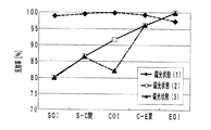
図6は、光ビームBの偏光状態が変化した場合における各反射部材24の反射率むらのシミュレーション結果を示すグラフである。図示した例では、三種類の偏光状態(1)〜(3)毎の反射率むらが示され、偏光状態が変わると、反射部材24の反射率むらも変化する。ここで、図6の偏光状態(1)〜(3)は、下記表1の通りである。
FIG. 6 is a graph showing a simulation result of the uneven reflectance of each reflecting

より具体的には、上記表1には、反射部材24への光ビームBの入射位置毎に、偏光状態の典型例としてp偏光比率が示される。表1において、COI(Center Of Imaging)は、被走査面29における有効走査域の中心像高およびその近傍に向かう光ビームBの入射位置であり、SOI(Start Of Imaging)およびEOI(End Of Imaging)は、同有効走査域における最大像高およびその近傍に向かう光ビームBの入射位置である。また、表1および図6には、上記以外にも、S−C間およびC−E間の偏光状態も示される。S−C間はSOIおよびCOIの中間位置であり、C−E間はCOIおよびEOIの中間位置である。
More specifically, Table 1 shows the p polarization ratio as a typical example of the polarization state for each incident position of the light beam B on the reflecting
また、反射部材24での入射位置毎の光ビームBの入射角度は、下記表2に示す通りである。特に、SOIおよびEOIでの入射角度は、51.8度であり、上記条件(A)を満たしている。
Further, the incident angle of the light beam B at each incident position on the reflecting
また、図7は、光ビームの偏光状態が変化した場合における被走査面29での光量むらのシミュレーション結果を示すグラフである。また、図8および図9は、本実施形態の反射部材24を、比較例の反射部材に置換したレーザ走査光学系において、偏光状態を変化させた場合における反射率むらおよび光量むらを示すシミュレーション結果を示すグラフである。図6および図7(本実施形態の反射部材の特性)と、図8および図9(比較例の反射部材の特性)を比較すれば分かるように、本実施形態の反射部材24での反射率むら、および本実施形態の被走査面29での光量むらが小さくなっている。
FIG. 7 is a graph showing a simulation result of unevenness in the amount of light on the scanned
また、図10は、本実施形態の反射部材24と、比較例の反射部材とにおける反射率むらの変化量のシミュレーション結果を示すグラフである。より具体的には、上記偏光状態(1)における反射率むらと、上記偏光状態(3)における反射率むらとの差を比較したものである。図10に示した通り、反射部材24における反射率むらの変化量は、従来のものと比較して小さい。
FIG. 10 is a graph showing a simulation result of the amount of change in reflectance unevenness between the reflecting
以上説明した通り、被走査面29の有効走査域における最大像高をとる両端位置に向かう光ビームの反射部材24への入射角が10度以上55度未満であれば、反射率むらを小さくすることが可能となる。 As described above, if the incident angle of the light beam toward the both end positions where the maximum image height in the effective scanning area of the surface to be scanned 29 is 10 degrees or more and less than 55 degrees, the reflectance unevenness is reduced. It becomes possible.
また、本願発明者は、上記入射角が10度以上55度未満の場合における、膜厚Dに対する反射率むらの最悪値をシミュレーションした。その結果を、図11に示す。図11のシミュレーション結果から、反射率むらを10%以下の小さな値に抑えるには、膜厚Dは0.15λよりも大きく、0.40λよりも小さくすればよいことが分かる。 Further, the inventor of the present application simulated the worst value of the reflectance unevenness with respect to the film thickness D when the incident angle is 10 degrees or more and less than 55 degrees. The result is shown in FIG. From the simulation result of FIG. 11, it can be seen that the film thickness D should be larger than 0.15λ and smaller than 0.40λ in order to suppress the reflectance unevenness to a small value of 10% or less.
(第一実施形態の作用・効果)
第一実施形態では、金属膜52および単層の光学薄膜53が蒸着された反射部材24〜26を利用した場合、光学薄膜53の膜厚Dが0.15λよりも大きくかつ0.4λよりも小さくされる(上記条件(B))。さらに、被走査面29上の有効走査域の両端に向かう光ビームBの反射部材24〜26への入射角が10度以上55度未満の範囲とされる(上記条件(A))。複屈折が大きな材料からなる走査光学素子を用いた場合であっても、二つの条件(A),(B)を満たせば、走査レンズ21〜23により光ビームBがどのような偏光状態となったとしても、反射部材24〜26における反射率むらは、10%以下という小さな値とすることができる。これにより、被走査面29上の光量むらへの悪影響を一定以下に抑えることが可能となる。
(Operation and effect of the first embodiment)
In the first embodiment, when the reflecting
また、入射角が10度以上55度未満の範囲におけるp偏光反射率とs偏光反射率の差も従来と比較して小さくすることが可能となるので、複屈折分布により、光ビームBの通過位置毎に偏光状態が変化し、反射部材24〜26への入射角毎にp偏光とs偏光との比率が変動した場合であっても反射率むらの変動を低減することが可能となる。
In addition, the difference between the p-polarized reflectance and the s-polarized reflectance in the range where the incident angle is not less than 10 degrees and less than 55 degrees can be reduced as compared with the conventional one. Even when the polarization state changes for each position and the ratio of p-polarized light to s-polarized light changes for each incident angle to the reflecting
また、第一実施形態では、各光源11は、走査レンズ21〜23のCOI近傍への入射光ビームBの直線偏光における振動方向が該光軸近傍の複屈折の軸方位と略同一となるように、配置される。これにより、複屈折による偏光状態の変化が生じなくなるので、被走査面29の有効走査域の中心像高近傍に向かう光ビームが反射部材24〜26に入射される際の偏光状態の予測が可能となる。よって、被走査面29での光量むらの一部最適化が可能となる。なお、この点については、第二および第三実施形態でも同様である。
Further, in the first embodiment, each
また、走査レンズ21〜23の光軸近傍では、一般的に、軸方位が副走査方向と略同一であることが知られている。それゆえ、第一実施形態では、各光源11は、直線偏光の振動方向が偏向器17のポリゴンミラーの回転軸A(後述)の方向と概ね一致するように配置される。その結果、被走査面29の有効走査域の中心像高近傍に向かう光ビームBの直線偏光の振動方向は、上記走査レンズ21〜23の光軸近傍への入射時に、該走査レンズ21〜23の光軸近傍の複屈折の軸方位と一致する。それゆえ、被走査面29の有効走査域の中心像高近傍に向かう光ビームBには、複屈折による偏光状態の変化が生じないので、光ビームBは、反射部材24〜26の入射面に対して直線偏光の振動方向が略平行のまま該反射部材24〜26に入射される。
In addition, it is generally known that the axial direction is substantially the same as the sub-scanning direction in the vicinity of the optical axis of the
上記のように、入射面に対する直線偏光の振動方向が略平行のままであれば、入射光ビームBはほぼp偏光成分のみとなる。よって、被走査面29の有効走査域の中心像高近傍に向かう光ビームBの反射部材24〜26での反射率はほぼp偏光反射率によって決まることになる。この反射率は、被走査面29の有効走査域に中心像高近傍以外に向かう光ビームBの反射部材24〜26での反射率のとりうる範囲(s偏光反射率からp偏光反射率まで)の平均に近い範囲に収まる。よって、被走査面29の中心像高近傍に対する中心像高近傍以外の光量むらは一定以下に抑えることが可能となる。この点についても、第二実施形態および第三実施形態でも同様に当てはまる。
As described above, if the vibration direction of the linearly polarized light with respect to the incident surface remains substantially parallel, the incident light beam B has substantially only the p-polarized component. Therefore, the reflectance of the light beam B toward the vicinity of the center image height in the effective scanning area of the scanned
また、第一実施形態では、一つの光路において、三個の走査レンズ21〜23が設けられ、各走査レンズ21〜23は、光弾性係数が20×10-12[Pa-1]以上の材料からなる。この場合、複屈折による偏光状態の変動が大きくなるため、その変動を予測することは非常に困難となる。この条件下では、第一実施形態のような反射部材24〜26を採用することは非常に効果的である。なお、二個以上の走査レンズ21〜23のうち二個の光弾性係数が20×10-12[Pa-1]以上の場合でも、偏光状態の変動を予測することは困難であるため、第一実施形態のような反射部材24〜26を採用することは効果的である。この点については、第二実施形態でも同様に当てはまる。
In the first embodiment, three
また、第一実施形態では、各走査レンズ21〜23として、画角が80度以上のものが用いられる。この場合、画角に対する入射角の範囲が大きく、複屈折による反射率むらが大きくなりやすくなる。それゆえ、第一実施形態のような反射部材24〜26を採用することは非常に効果的である。この点については、第二実施形態および第三実施形態でも同様に当てはまる。
In the first embodiment, each of the
また、第一実施形態のレーザ走査光学系は、複数の光源11および複数の被走査面29を備え、光源11および被走査面29の組み毎に光路が設けられる。各光路に共通走査レンズ21,22が配置されても、配置されなくとも、複屈折による偏光状態の変動は光路毎で異なる。それゆえ、一つ以上の光路に対し、第一実施形態のような反射部材24〜26が配置されることが効果的である。また、偏向器17への入射光ビームが副走査方向に対し角度を有する場合にも、効果的となる。この点について、第二実施形態にも同様に当てはまる。
The laser scanning optical system according to the first embodiment includes a plurality of
(第二実施形態)
上記第一実施形態では、片側偏向を採用したレーザ走査光学系に各反射部材24〜26を適用した例が示されていた。しかし、これに限らず、図12および図13に示すような両側偏向を採用したレーザ走査光学系に上記各反射部材24,25を適用しても、反射率むらおよび光量むらを小さくすることが可能となる。
(Second embodiment)
In the first embodiment, an example in which the reflecting
図12および図13では、要部にのみ参照符号を付し、図1および図2の構成に相当するものには同一の参照符号を付け、それぞれの説明を省略する。 12 and FIG. 13, reference numerals are given only to the main parts, the same reference numerals are assigned to the components corresponding to the configurations of FIG. 1 and FIG. 2, and the descriptions thereof are omitted.
また、両側偏向のレーザ走査光学系では、例えば光ビームBaの光路と、光ビームBdの光路とが偏向器17の回転軸Aを含む平面に対して概ね対称に、また、光ビームBbの光路と、光ビームBcの光路とが同平面に対して概ね対称になるよう、各構成が配置される。それゆえ、以下の説明では、光ビームBa,Bbの光路について説明し、光ビームBc,Bdの光路の説明を省略する。
In the both-side deflection laser scanning optical system, for example, the optical path of the light beam Ba and the optical path of the light beam Bd are substantially symmetric with respect to the plane including the rotation axis A of the
図12および図13において、光源11a,11bからの光ビームBa,Bbは、シリンドリカルレンズ16等を介して偏向器17のポリゴンミラーに入射される。
12 and 13, light beams Ba and Bb from the
偏向器17は、ポリゴンミラーのある一面を用いて、入射光ビームBa,Bbを主走査方向に偏向する。共通走査レンズ21,22は、偏向器17で偏向された光ビームBa,Bbの光路上で、上流側および下流側に配置される。また、光ビームBa,Bbの光路上で、共通走査レンズ22の下流側には、個別走査レンズ23a,23bが配置される。
The
第一反射部材24a,24bは、光ビームBa,Bbの光路上で、共通走査レンズ22の下流側で、かつ個別走査レンズ23a,23bの上流に設けられる。また、第二反射部材25bは、個別走査レンズ23bの下流側に設けられる。
The first reflecting
第一反射部材24a,24bは、共通走査レンズ22を通過した光ビームBa,Bbが入射されると、入射光ビームBa,Bbを個別走査レンズ23a,23bに向けて反射する。個別走査レンズ23aを透過した光ビームBaは、防塵用ウインドウ27aを通過して、被走査面29aで結像する。個別走査レンズ23bを透過した光ビームBbは、第二反射部材25bで反射された後、防塵用ウインドウ27bを通過して、被走査面29bで結像する。
When the light beams Ba and Bb having passed through the
(反射部材の詳細について)
本実施形態でも、各反射部材24,25は、第一実施形態と同様の条件(A),(B)を満たすよう配置および形成される。ここで、図14を参照して、反射部材24,25への入射角に対するp偏光およびs偏光の反射率の特性(以下、入射角特性という)を説明する。図14中、横軸は入射角であり、縦軸は反射率である。また、光学薄膜53の膜厚は0.375λである。
(Details of reflective member)
Also in this embodiment, each
反射部材24での反射率むらが最大となる条件(C)について詳細に述べると、図14の例においても、両端に向かう光ビームの入射角が55度未満であれば、反射率むらを相対的に小さくすることが可能となる。ただし、設計上、両端に向かう光ビームの入射角が10度未満の範囲で反射部材24,25を使用することは無い。このような観点で、本実施形態でも、反射部材24,25への入射光ビームのうち、被走査面29の有効走査域における最大像高をとる両端位置に向かう光ビームの入射角が10度以上55度未満とする。
Describing in detail the condition (C) at which the reflectance unevenness at the reflecting
ここで、図15は、本実施形態の反射部材24の反射率むらの変化量と、比較例の反射部材(第一実施形態を参照)とにおける反射率むらの変化量とのシミュレーション結果を示すグラフである。図15においても、第一実施形態と同様、上記表1の偏光状態(1)と偏光状態(3)の反射率むらの差が示されている。また、反射部材24への光ビームBの入射角度および比較例の反射部材への光ビームの入射角度は、下記表3に示す通りである。
Here, FIG. 15 shows a simulation result of the variation amount of the reflectance unevenness of the
図15に示す場合においても、本実施形態に係る反射部材24における反射率むらの変化量は、従来のものと比較して小さくなっている。
Also in the case shown in FIG. 15, the amount of change in the reflectance unevenness in the reflecting
また、膜厚Dに関しては、第一実施形態で図11を参照して説明したのと同様に、反射率むらを約10%以下に抑えるには、光学薄膜53の膜厚を0.15λよりも大きく、0.40λよりも小さくすればよいことが分かる。
Regarding the film thickness D, as described with reference to FIG. 11 in the first embodiment, the film thickness of the optical
(第二実施形態の作用・効果)
第二実施形態でも、第一実施形態と同様に、反射部材24〜26の反射率むらを10%以下に抑えることで、被走査面上の光量むらへの悪影響を一定以下に抑えることが可能となる。
(Operation / Effect of Second Embodiment)
Also in the second embodiment, similarly to the first embodiment, by suppressing the uneven reflectance of the reflecting
(第三実施形態)
第三実施形態に係るレーザ走査光学系は、典型的にはモノクロプリンタのような画像形成装置に適用される。このレーザ走査光学系は、図16および図17に示すように、大略的に、光源61、コリメータレンズ62、シリンドリカルレンズ66、偏向器67、単一の走査レンズ71、反射部材72および感光体ドラム68を備える。感光体ドラム68は、被走査面69を有しており、図示しないモータからの駆動力により副走査方向に回転する。また、回転する被走査面69には、下記の光ビームBが主走査方向に1ラインずつ順次的に走査される。
(Third embodiment)
The laser scanning optical system according to the third embodiment is typically applied to an image forming apparatus such as a monochrome printer. As shown in FIGS. 16 and 17, the laser scanning optical system generally includes a
光源61は、単一の光路の最上流位置に設けられ、光ビームBを出射する。より具体的には、光源11は、画像データが自身に入力されると、入力画像データで変調された光ビームBを出射する。
The
ここで、光源61の好ましい配置条件は、第一実施形態で説明した光源11の好ましい配置条件と同様である。
Here, the preferable arrangement conditions of the
コリメータレンズ62は、光源61に対し下流側に設けられ、光ビームBを平行光に変換する。シリンドリカルレンズ66は、平行光となった光ビームBを、偏向器67のポリゴンミラーの反射面で線状に結像するように集光する。偏向器67は、モータ(図示せず)と、ポリゴンミラーとを有する。偏向器67において、ポリゴンミラーは、モータの駆動力によって回転軸Aを中心として回転し、これによって、シリンドリカルレンズ66から出射された光ビームBを主走査方向に偏向する。
The
走査レンズ71は、偏向器67からの入射光ビームBの走査速度を一定にすると共に、光ビームBの径を均一とする光学特性を有する。このような走査レンズ71は、主に低コスト化の観点から、複屈折が大きな材料(つまり、光弾性係数が20×10-12[Pa-1]以上の材料)からなる。また、走査レンズ71の画角は80度以上である。その具体例として、走査レンズ71は、光弾性係数が43×10-12[Pa-1]のポリカーボネートのような熱可塑性樹脂からなり、96度の画角を有する。
The
反射部材72は、走査レンズ71を通過した光ビームBが入射されると、入射光ビームBを被走査面69に向けて反射して、該被走査面69で結像させる。
When the light beam B that has passed through the
(反射部材の詳細について)
反射部材72は、第一実施形態の反射部材24と同様に、基材51と、該基材51に蒸着された金属膜52および単層の光学薄膜53と、を含んでいる(図3を参照)。
(Details of reflective member)
The
本実施形態では、反射部材72は、以下の条件(A’),(B’)を満たす。
(A’)反射部材72への入射光ビームのうち、被走査面69の有効走査域における最大像高をとる両端位置に向かう光ビームの入射角が55度以上69度未満とする。
(B’)各光学薄膜53の膜厚を0.18λよりも大きく0.22λよりも小さくする、もしくは、0.36λよりも大きく0.41λよりも小さくする。ここで、λは光ビームの波長である。
In the present embodiment, the reflecting
(A ′) Of the incident light beam to the reflecting
(B ′) The film thickness of each optical
ここで、図4を参照して、反射部材72(膜厚Dが0.20λ)への入射角に対するp偏光およびs偏光の反射率の特性(以下、入射角特性という)を説明する。反射部材72もまた入射角特性を有しており、その結果、反射部材72では反射率むらが発生する。この反射部材72でも反射率むらが最大となるのは、第一実施形態で述べた(C),(D)の場合である。
Here, with reference to FIG. 4, the reflectance characteristics of p-polarized light and s-polarized light with respect to the incident angle to the reflecting member 72 (film thickness D is 0.20λ) (hereinafter referred to as incident angle characteristics) will be described. The
(C)について詳細に述べると、両端に向かう光ビームの入射角が55度以上69度未満であっても、69度以上の場合と比較して、反射率むらは相対的に小さくなる。それゆえ、本実施形態では、反射部材72への入射光ビームのうち、被走査面29の有効走査域における最大像高をとる両端位置に向かう光ビームの入射角は55度以上69度未満に設定される。
When (C) is described in detail, even if the incident angle of the light beam toward both ends is 55 degrees or more and less than 69 degrees, the reflectance unevenness is relatively small as compared with the case of 69 degrees or more. Therefore, in the present embodiment, the incident angle of the light beam toward the both end positions taking the maximum image height in the effective scanning area of the scanned
図18は、光ビームの偏光状態が変化した場合における反射部材72の反射率むらのシミュレーション結果を示すグラフである。図示した例では、三種類の偏光状態(1)〜(3)毎の反射率むらが示され、偏光状態が変わると、反射部材72の反射率むらも変化する。なお、偏光状態(1)〜(3)は、上記表1の通りである。
FIG. 18 is a graph showing a simulation result of uneven reflectance of the reflecting
また、反射部材72での入射位置毎の光ビームBの入射角度は、下記表4に示す通りである。
Further, the incident angle of the light beam B at each incident position on the reflecting
また、図19は、光ビームの偏光状態が変化した場合における被走査面69での光量むらのシミュレーション結果を示すグラフである。また、図20および図21は、本実施形態の反射部材72を、比較例の反射部材に置換したレーザ走査光学系において、偏光状態を変化させた場合における反射率むらおよび光量むらを示すシミュレーション結果を示すグラフである。図18および図19(本実施形態の反射部材)と、図20および図21(比較例の反射部材)を比較すれば分かるように、本実施形態の反射部材72での反射率むら、および本実施形態の被走査面69での光量むらが小さくなっている。
FIG. 19 is a graph showing a simulation result of unevenness in the amount of light on the surface to be scanned 69 when the polarization state of the light beam changes. FIGS. 20 and 21 are simulation results showing the unevenness of reflectance and the amount of light when the polarization state is changed in the laser scanning optical system in which the reflecting
以上から分かるように、被走査面29の有効走査域における最大像高をとる両端位置に向かう光ビームの反射部材24への入射角が55度以上69度未満としても、反射率むらを小さくすることが可能である。
As can be seen from the above, even when the incident angle of the light beam toward the both end positions where the maximum image height in the effective scanning area of the surface to be scanned 29 reaches the reflecting
また、図22は、上記入射角が55度以上69度未満の場合における、光学薄膜53の膜厚に対する反射率むらの最悪値を示すシミュレーション結果である。図22に示すように、反射率むらを小さく抑えるには、光学薄膜53の膜厚を0.15λよりも大きく、0.40λよりも小さくすればよいことが分かる。
FIG. 22 is a simulation result showing the worst value of the reflectance unevenness with respect to the film thickness of the optical
また、本願発明者は、上記入射角が55度以上69度未満の場合における、膜厚Dに対する反射率むらの最悪値をシミュレーションした。その結果を、図22に示す。図22のシミュレーション結果から、膜厚Dは0.15λよりも大きく、0.40λよりも小さくすれば、反射率むらを10%以下の小さな値にすることができる。 The inventor of the present application simulated the worst value of the reflectance unevenness with respect to the film thickness D when the incident angle is 55 degrees or more and less than 69 degrees. The result is shown in FIG. From the simulation result of FIG. 22, if the film thickness D is larger than 0.15λ and smaller than 0.40λ, the reflectance unevenness can be made a small value of 10% or less.
(第三実施形態の作用・効果)
第三実施形態では、金属膜52および単層の光学薄膜53が蒸着された反射部材72を利用した場合、光学薄膜53の膜厚Dが0.18λ<D<0.22λまたは0.36λ<D<0.41の範囲とされる(上記条件(B’))。さらに、被走査面69での有効走査域の両端に向かう光ビームBの反射部材24〜26への入射角が55度以上69度未満の範囲とされる(上記条件(A’))。複屈折が大きな材料からなる走査光学素子を用いた場合であっても、二つの条件(A’),(B’)を満たせば、走査レンズ71により光ビームBがどのような偏光状態となったとしても、反射部材72における反射率むらは、10%以下という小さな値とすることができる。これにより、被走査面69上の光量むらへの悪影響を一定以下に抑えることが可能となる。
(Operation and effect of the third embodiment)
In the third embodiment, when the reflecting
また、入射角が55度以上69度未満の範囲におけるp偏光反射率とs偏光反射率の差も従来と比較して小さくすることが可能となるので、複屈折分布により、光ビームBの通過位置毎に偏光状態が変化し、反射部材72への入射角毎にp偏光とs偏光との比率が変動した場合であっても反射率むらの変動を低減することが可能となる。
In addition, since the difference between the p-polarized reflectance and the s-polarized reflectance in the range where the incident angle is 55 degrees or more and less than 69 degrees can be reduced as compared with the conventional case, the light beam B passes through the birefringence distribution. Even when the polarization state changes for each position and the ratio of the p-polarized light and the s-polarized light changes for each incident angle to the reflecting
特に、第三実施形態では、レーザ走査光学系は、単一の走査レンズ71を備える。この場合にも、複屈折による偏光状態の変動があるため、反射部材72により反射率むらの変動を低減することが可能となる。
In particular, in the third embodiment, the laser scanning optical system includes a
本発明に係るレーザ走査光学系は、複屈折が大きな材料からなる走査光学素子を用いた場合でも、被走査面上での光量むらの変化を低減可能であり、MFPやモノクロプリンタ以外にも、コピー機、カラープリンタ、ファクシミリ等に有用である。 The laser scanning optical system according to the present invention can reduce the variation in the amount of light unevenness on the surface to be scanned even when a scanning optical element made of a material having a large birefringence is used. Useful for copiers, color printers, facsimiles, etc.
11,61 光源
17,67 偏向器
20 走査光学素子群
21,22 共通走査レンズ
23 個別走査レンズ
24 第一反射部材
25 第二反射部材
26 第三反射部材
28,68 感光体ドラム
29,69 被走査面
51 基材
52 金属膜
53 光学薄膜
71 走査レンズ
72 反射部材
A 回転軸
B 光ビーム
D 膜厚
11, 61
Claims (8)
前記光源から出射された光ビームを偏向する偏向手段と、
光弾性係数が20×10-12[Pa-1]以上の材料からなり、前記偏向手段により偏向された光ビームを被走査面上に結像させる、一つ以上の走査光学素子と、
前記一つ以上の走査光学素子を透過した光ビームが入射されると、該入射光ビームを前記被走査面に向けて反射する、一つ以上の反射部材と、を備え、
少なくとも一つの前記走査光学素子は、光弾性係数が20×10-12[Pa-1]以上の材料からなり、
前記反射部材は、基板と、該基板に蒸着された金属膜および単層の光学薄膜と、を含み、
前記光ビームの波長をλとし、前記単層の光学薄膜の膜厚をDとすると、Dは、0.36λ<D<0.41λであり、
前記被走査面の有効走査域の最大像高の両端に向かう光ビームの、前記反射部材への入射角は55度以上69度未満とし、
前記被走査面のCOI(Center Of Imaging)近傍への入射光ビームの直線偏光の振動方向が、前記少なくとも一つの走査光学素子の光軸近傍の複屈折の軸方位と略同一になるように、前記光源は配置される、レーザ走査光学系。 A light source that emits a linearly polarized light beam;
Deflecting means for deflecting the light beam emitted from the light source;
One or more scanning optical elements made of a material having a photoelastic coefficient of 20 × 10 −12 [Pa −1 ] or more and forming an image of the light beam deflected by the deflecting unit on the surface to be scanned;
One or more reflecting members that reflect the incident light beam toward the scanned surface when a light beam transmitted through the one or more scanning optical elements is incident;
At least one of the scanning optical elements is made of a material having a photoelastic coefficient of 20 × 10 −12 [Pa −1 ] or more,
The reflective member includes a substrate, a metal film deposited on the substrate, and a single-layer optical thin film,
Assuming that the wavelength of the light beam is λ and the film thickness of the single-layer optical thin film is D, D is 0 . 36λ <D <0.41λ,
The incident angle of the light beam toward both ends of the maximum image height in the effective scanning area of the surface to be scanned is 55 degrees or more and less than 69 degrees ,
The vibration direction of the linearly polarized light of the incident light beam near the COI (Center Of Imaging) of the surface to be scanned is substantially the same as the birefringence axis direction near the optical axis of the at least one scanning optical element. A laser scanning optical system in which the light source is arranged.
Priority Applications (2)
| Application Number | Priority Date | Filing Date | Title |
|---|---|---|---|
| JP2012086921A JP5724932B2 (en) | 2012-04-06 | 2012-04-06 | Laser scanning optical system |
| US13/857,784 US10088674B2 (en) | 2012-04-06 | 2013-04-05 | Laser scanning optical system |
Applications Claiming Priority (1)
| Application Number | Priority Date | Filing Date | Title |
|---|---|---|---|
| JP2012086921A JP5724932B2 (en) | 2012-04-06 | 2012-04-06 | Laser scanning optical system |
Publications (2)
| Publication Number | Publication Date |
|---|---|
| JP2013218038A JP2013218038A (en) | 2013-10-24 |
| JP5724932B2 true JP5724932B2 (en) | 2015-05-27 |
Family
ID=49292097
Family Applications (1)
| Application Number | Title | Priority Date | Filing Date |
|---|---|---|---|
| JP2012086921A Active JP5724932B2 (en) | 2012-04-06 | 2012-04-06 | Laser scanning optical system |
Country Status (2)
| Country | Link |
|---|---|
| US (1) | US10088674B2 (en) |
| JP (1) | JP5724932B2 (en) |
Family Cites Families (16)
| Publication number | Priority date | Publication date | Assignee | Title |
|---|---|---|---|---|
| JP2727572B2 (en) | 1988-07-26 | 1998-03-11 | キヤノン株式会社 | Optical scanning device |
| KR960035077A (en) * | 1995-03-22 | 1996-10-24 | 이형도 | Scanning optics |
| JPH1184106A (en) * | 1997-09-12 | 1999-03-26 | Ricoh Co Ltd | Lens |
| JP2001337285A (en) * | 2000-05-29 | 2001-12-07 | Minolta Co Ltd | Optical scanner |
| JP4708637B2 (en) * | 2000-09-29 | 2011-06-22 | キヤノン株式会社 | Multi-beam scanning optical apparatus and image forming apparatus using the same |
| JP4566398B2 (en) * | 2000-12-13 | 2010-10-20 | キヤノン株式会社 | Optical scanning device, multi-beam scanning device, and image forming apparatus |
| JP4296011B2 (en) * | 2003-03-13 | 2009-07-15 | 株式会社リコー | Optical scanning apparatus and image forming apparatus |
| JP4330489B2 (en) * | 2004-05-17 | 2009-09-16 | コニカミノルタビジネステクノロジーズ株式会社 | Laser scanner |
| JP4522253B2 (en) * | 2004-12-24 | 2010-08-11 | キヤノン株式会社 | Optical scanning device and image display device using the same |
| US7807239B2 (en) * | 2005-11-21 | 2010-10-05 | Nitto Denko Corporation | Optical film containing polymer having naphtyl group |
| JP2007156172A (en) * | 2005-12-06 | 2007-06-21 | Canon Inc | Optical scanner and image forming apparatus using the same |
| JP5072613B2 (en) * | 2008-01-18 | 2012-11-14 | キヤノン株式会社 | Optical scanning device and image forming apparatus using the same |
| JP5511226B2 (en) * | 2009-06-04 | 2014-06-04 | キヤノン株式会社 | Scanning optical device and image forming apparatus using the same |
| JP5321331B2 (en) * | 2009-08-03 | 2013-10-23 | 株式会社リコー | Optical scanning apparatus and image forming apparatus |
| JP5278253B2 (en) * | 2009-09-02 | 2013-09-04 | 株式会社リコー | Optical scanning apparatus and image forming apparatus |
| JP5609994B2 (en) * | 2011-01-24 | 2014-10-22 | コニカミノルタ株式会社 | Zoom lens, imaging optical device and digital device |
-
2012
- 2012-04-06 JP JP2012086921A patent/JP5724932B2/en active Active
-
2013
- 2013-04-05 US US13/857,784 patent/US10088674B2/en active Active
Also Published As
| Publication number | Publication date |
|---|---|
| US20130265627A1 (en) | 2013-10-10 |
| JP2013218038A (en) | 2013-10-24 |
| US10088674B2 (en) | 2018-10-02 |
Similar Documents
| Publication | Publication Date | Title |
|---|---|---|
| JP6047107B2 (en) | Optical scanning device and image forming apparatus having the same | |
| JP2008076557A (en) | Optical scanner and image forming apparatus using the same | |
| JP4634881B2 (en) | Optical scanning device and image forming device | |
| JP5968040B2 (en) | Optical scanning apparatus, image forming apparatus, and optical scanning apparatus control method | |
| JP6140971B2 (en) | Optical scanning apparatus and image forming apparatus | |
| JP5072613B2 (en) | Optical scanning device and image forming apparatus using the same | |
| JP5724932B2 (en) | Laser scanning optical system | |
| JP4817668B2 (en) | Optical scanning device | |
| JP4174226B2 (en) | Optical scanning optical system and image forming apparatus using the same | |
| JP5511226B2 (en) | Scanning optical device and image forming apparatus using the same | |
| JP5661507B2 (en) | Scanning optical device and image forming apparatus using the same | |
| JP5423760B2 (en) | Laser scanning optical device | |
| JP2012150153A (en) | Optical scanner and image forming device | |
| JP2018101028A (en) | Optical scanner and image forming apparatus using the same | |
| JP6132701B2 (en) | Optical scanning device and image forming apparatus using the same | |
| JP5173567B2 (en) | Scanning optical device and image forming apparatus using the same | |
| JP2014006277A (en) | Optical scanner and image forming apparatus | |
| JP2014016404A (en) | Optical scanner and color image forming apparatus | |
| JP5874150B2 (en) | Laser scanning optical device | |
| JP2006091879A (en) | Optical scanner | |
| JP2008015140A (en) | Image forming apparatus | |
| JP4323752B2 (en) | Scanning optical device and image forming apparatus using the same | |
| JP2005331595A (en) | Optical scanner and image forming apparatus using same | |
| US20100155581A1 (en) | Laser scanning unit and image-forming apparatus having the same | |
| JP2013160934A (en) | Optical scanner and image forming apparatus |
Legal Events
| Date | Code | Title | Description |
|---|---|---|---|
| A621 | Written request for application examination |
Free format text: JAPANESE INTERMEDIATE CODE: A621 Effective date: 20140313 |
|
| A977 | Report on retrieval |
Free format text: JAPANESE INTERMEDIATE CODE: A971007 Effective date: 20140716 |
|
| A131 | Notification of reasons for refusal |
Free format text: JAPANESE INTERMEDIATE CODE: A131 Effective date: 20140729 |
|
| A521 | Request for written amendment filed |
Free format text: JAPANESE INTERMEDIATE CODE: A523 Effective date: 20140929 |
|
| TRDD | Decision of grant or rejection written | ||
| A01 | Written decision to grant a patent or to grant a registration (utility model) |
Free format text: JAPANESE INTERMEDIATE CODE: A01 Effective date: 20150303 |
|
| A61 | First payment of annual fees (during grant procedure) |
Free format text: JAPANESE INTERMEDIATE CODE: A61 Effective date: 20150316 |
|
| R150 | Certificate of patent or registration of utility model |
Ref document number: 5724932 Country of ref document: JP Free format text: JAPANESE INTERMEDIATE CODE: R150 |