JP5649547B2 - Manufacturing method of semiconductor device - Google Patents
Manufacturing method of semiconductor device Download PDFInfo
- Publication number
- JP5649547B2 JP5649547B2 JP2011224285A JP2011224285A JP5649547B2 JP 5649547 B2 JP5649547 B2 JP 5649547B2 JP 2011224285 A JP2011224285 A JP 2011224285A JP 2011224285 A JP2011224285 A JP 2011224285A JP 5649547 B2 JP5649547 B2 JP 5649547B2
- Authority
- JP
- Japan
- Prior art keywords
- cavity
- resin
- light receiving
- lead
- receiving element
- Prior art date
- Legal status (The legal status is an assumption and is not a legal conclusion. Google has not performed a legal analysis and makes no representation as to the accuracy of the status listed.)
- Active
Links
- 239000004065 semiconductor Substances 0.000 title claims description 25
- 238000004519 manufacturing process Methods 0.000 title claims description 15
- 229920005989 resin Polymers 0.000 claims description 62
- 239000011347 resin Substances 0.000 claims description 62
- 238000000465 moulding Methods 0.000 claims description 19
- 239000010409 thin film Substances 0.000 claims description 17
- 238000000034 method Methods 0.000 claims description 10
- 238000010586 diagram Methods 0.000 description 8
- 239000003822 epoxy resin Substances 0.000 description 4
- 238000009413 insulation Methods 0.000 description 4
- 229920000647 polyepoxide Polymers 0.000 description 4
- 239000010931 gold Substances 0.000 description 3
- 230000001902 propagating effect Effects 0.000 description 2
- 238000004080 punching Methods 0.000 description 2
- OKTJSMMVPCPJKN-UHFFFAOYSA-N Carbon Chemical compound [C] OKTJSMMVPCPJKN-UHFFFAOYSA-N 0.000 description 1
- XUIMIQQOPSSXEZ-UHFFFAOYSA-N Silicon Chemical compound [Si] XUIMIQQOPSSXEZ-UHFFFAOYSA-N 0.000 description 1
- BQCADISMDOOEFD-UHFFFAOYSA-N Silver Chemical compound [Ag] BQCADISMDOOEFD-UHFFFAOYSA-N 0.000 description 1
- GWEVSGVZZGPLCZ-UHFFFAOYSA-N Titan oxide Chemical compound O=[Ti]=O GWEVSGVZZGPLCZ-UHFFFAOYSA-N 0.000 description 1
- 239000004840 adhesive resin Substances 0.000 description 1
- 229920006223 adhesive resin Polymers 0.000 description 1
- 230000005540 biological transmission Effects 0.000 description 1
- 229910052799 carbon Inorganic materials 0.000 description 1
- 230000008878 coupling Effects 0.000 description 1
- 238000010168 coupling process Methods 0.000 description 1
- 238000005859 coupling reaction Methods 0.000 description 1
- 230000009977 dual effect Effects 0.000 description 1
- PCHJSUWPFVWCPO-UHFFFAOYSA-N gold Chemical compound [Au] PCHJSUWPFVWCPO-UHFFFAOYSA-N 0.000 description 1
- 229910052737 gold Inorganic materials 0.000 description 1
- 238000002347 injection Methods 0.000 description 1
- 239000007924 injection Substances 0.000 description 1
- 238000001746 injection moulding Methods 0.000 description 1
- 239000002184 metal Substances 0.000 description 1
- 229910052751 metal Inorganic materials 0.000 description 1
- 238000012986 modification Methods 0.000 description 1
- 230000004048 modification Effects 0.000 description 1
- 230000003287 optical effect Effects 0.000 description 1
- 239000000843 powder Substances 0.000 description 1
- 230000035945 sensitivity Effects 0.000 description 1
- 229910021332 silicide Inorganic materials 0.000 description 1
- FVBUAEGBCNSCDD-UHFFFAOYSA-N silicide(4-) Chemical compound [Si-4] FVBUAEGBCNSCDD-UHFFFAOYSA-N 0.000 description 1
- 229910052710 silicon Inorganic materials 0.000 description 1
- 239000010703 silicon Substances 0.000 description 1
- 229910052709 silver Inorganic materials 0.000 description 1
- 239000004332 silver Substances 0.000 description 1
- OGIDPMRJRNCKJF-UHFFFAOYSA-N titanium oxide Inorganic materials [Ti]=O OGIDPMRJRNCKJF-UHFFFAOYSA-N 0.000 description 1
Images


Classifications
-
- H—ELECTRICITY
- H10—SEMICONDUCTOR DEVICES; ELECTRIC SOLID-STATE DEVICES NOT OTHERWISE PROVIDED FOR
- H10F—INORGANIC SEMICONDUCTOR DEVICES SENSITIVE TO INFRARED RADIATION, LIGHT, ELECTROMAGNETIC RADIATION OF SHORTER WAVELENGTH OR CORPUSCULAR RADIATION
- H10F55/00—Radiation-sensitive semiconductor devices covered by groups H10F10/00, H10F19/00 or H10F30/00 being structurally associated with electric light sources and electrically or optically coupled thereto
- H10F55/18—Radiation-sensitive semiconductor devices covered by groups H10F10/00, H10F19/00 or H10F30/00 being structurally associated with electric light sources and electrically or optically coupled thereto wherein the radiation-sensitive semiconductor devices and the electric light source share a common body having dual-functionality of light emission and light detection
-
- H—ELECTRICITY
- H10—SEMICONDUCTOR DEVICES; ELECTRIC SOLID-STATE DEVICES NOT OTHERWISE PROVIDED FOR
- H10F—INORGANIC SEMICONDUCTOR DEVICES SENSITIVE TO INFRARED RADIATION, LIGHT, ELECTROMAGNETIC RADIATION OF SHORTER WAVELENGTH OR CORPUSCULAR RADIATION
- H10F55/00—Radiation-sensitive semiconductor devices covered by groups H10F10/00, H10F19/00 or H10F30/00 being structurally associated with electric light sources and electrically or optically coupled thereto
- H10F55/20—Radiation-sensitive semiconductor devices covered by groups H10F10/00, H10F19/00 or H10F30/00 being structurally associated with electric light sources and electrically or optically coupled thereto wherein the electric light source controls the radiation-sensitive semiconductor devices, e.g. optocouplers
- H10F55/25—Radiation-sensitive semiconductor devices covered by groups H10F10/00, H10F19/00 or H10F30/00 being structurally associated with electric light sources and electrically or optically coupled thereto wherein the electric light source controls the radiation-sensitive semiconductor devices, e.g. optocouplers wherein the radiation-sensitive devices and the electric light source are all semiconductor devices
- H10F55/255—Radiation-sensitive semiconductor devices covered by groups H10F10/00, H10F19/00 or H10F30/00 being structurally associated with electric light sources and electrically or optically coupled thereto wherein the electric light source controls the radiation-sensitive semiconductor devices, e.g. optocouplers wherein the radiation-sensitive devices and the electric light source are all semiconductor devices formed in, or on, a common substrate
-
- H—ELECTRICITY
- H10—SEMICONDUCTOR DEVICES; ELECTRIC SOLID-STATE DEVICES NOT OTHERWISE PROVIDED FOR
- H10F—INORGANIC SEMICONDUCTOR DEVICES SENSITIVE TO INFRARED RADIATION, LIGHT, ELECTROMAGNETIC RADIATION OF SHORTER WAVELENGTH OR CORPUSCULAR RADIATION
- H10F77/00—Constructional details of devices covered by this subclass
- H10F77/50—Encapsulations or containers
-
- H—ELECTRICITY
- H10—SEMICONDUCTOR DEVICES; ELECTRIC SOLID-STATE DEVICES NOT OTHERWISE PROVIDED FOR
- H10F—INORGANIC SEMICONDUCTOR DEVICES SENSITIVE TO INFRARED RADIATION, LIGHT, ELECTROMAGNETIC RADIATION OF SHORTER WAVELENGTH OR CORPUSCULAR RADIATION
- H10F77/00—Constructional details of devices covered by this subclass
- H10F77/93—Interconnections
- H10F77/933—Interconnections for devices having potential barriers
-
- H—ELECTRICITY
- H10—SEMICONDUCTOR DEVICES; ELECTRIC SOLID-STATE DEVICES NOT OTHERWISE PROVIDED FOR
- H10H—INORGANIC LIGHT-EMITTING SEMICONDUCTOR DEVICES HAVING POTENTIAL BARRIERS
- H10H20/00—Individual inorganic light-emitting semiconductor devices having potential barriers, e.g. light-emitting diodes [LED]
- H10H20/01—Manufacture or treatment
-
- H—ELECTRICITY
- H01—ELECTRIC ELEMENTS
- H01L—SEMICONDUCTOR DEVICES NOT COVERED BY CLASS H10
- H01L2224/00—Indexing scheme for arrangements for connecting or disconnecting semiconductor or solid-state bodies and methods related thereto as covered by H01L24/00
- H01L2224/01—Means for bonding being attached to, or being formed on, the surface to be connected, e.g. chip-to-package, die-attach, "first-level" interconnects; Manufacturing methods related thereto
- H01L2224/42—Wire connectors; Manufacturing methods related thereto
- H01L2224/44—Structure, shape, material or disposition of the wire connectors prior to the connecting process
- H01L2224/45—Structure, shape, material or disposition of the wire connectors prior to the connecting process of an individual wire connector
- H01L2224/45001—Core members of the connector
- H01L2224/45099—Material
- H01L2224/451—Material with a principal constituent of the material being a metal or a metalloid, e.g. boron (B), silicon (Si), germanium (Ge), arsenic (As), antimony (Sb), tellurium (Te) and polonium (Po), and alloys thereof
- H01L2224/45138—Material with a principal constituent of the material being a metal or a metalloid, e.g. boron (B), silicon (Si), germanium (Ge), arsenic (As), antimony (Sb), tellurium (Te) and polonium (Po), and alloys thereof the principal constituent melting at a temperature of greater than or equal to 950°C and less than 1550°C
- H01L2224/45144—Gold (Au) as principal constituent
-
- H—ELECTRICITY
- H01—ELECTRIC ELEMENTS
- H01L—SEMICONDUCTOR DEVICES NOT COVERED BY CLASS H10
- H01L2224/00—Indexing scheme for arrangements for connecting or disconnecting semiconductor or solid-state bodies and methods related thereto as covered by H01L24/00
- H01L2224/01—Means for bonding being attached to, or being formed on, the surface to be connected, e.g. chip-to-package, die-attach, "first-level" interconnects; Manufacturing methods related thereto
- H01L2224/42—Wire connectors; Manufacturing methods related thereto
- H01L2224/47—Structure, shape, material or disposition of the wire connectors after the connecting process
- H01L2224/48—Structure, shape, material or disposition of the wire connectors after the connecting process of an individual wire connector
- H01L2224/4805—Shape
- H01L2224/4809—Loop shape
- H01L2224/48091—Arched
-
- H—ELECTRICITY
- H01—ELECTRIC ELEMENTS
- H01L—SEMICONDUCTOR DEVICES NOT COVERED BY CLASS H10
- H01L2224/00—Indexing scheme for arrangements for connecting or disconnecting semiconductor or solid-state bodies and methods related thereto as covered by H01L24/00
- H01L2224/01—Means for bonding being attached to, or being formed on, the surface to be connected, e.g. chip-to-package, die-attach, "first-level" interconnects; Manufacturing methods related thereto
- H01L2224/42—Wire connectors; Manufacturing methods related thereto
- H01L2224/47—Structure, shape, material or disposition of the wire connectors after the connecting process
- H01L2224/48—Structure, shape, material or disposition of the wire connectors after the connecting process of an individual wire connector
- H01L2224/481—Disposition
- H01L2224/48151—Connecting between a semiconductor or solid-state body and an item not being a semiconductor or solid-state body, e.g. chip-to-substrate, chip-to-passive
- H01L2224/48221—Connecting between a semiconductor or solid-state body and an item not being a semiconductor or solid-state body, e.g. chip-to-substrate, chip-to-passive the body and the item being stacked
- H01L2224/48245—Connecting between a semiconductor or solid-state body and an item not being a semiconductor or solid-state body, e.g. chip-to-substrate, chip-to-passive the body and the item being stacked the item being metallic
- H01L2224/48247—Connecting between a semiconductor or solid-state body and an item not being a semiconductor or solid-state body, e.g. chip-to-substrate, chip-to-passive the body and the item being stacked the item being metallic connecting the wire to a bond pad of the item
-
- H—ELECTRICITY
- H01—ELECTRIC ELEMENTS
- H01L—SEMICONDUCTOR DEVICES NOT COVERED BY CLASS H10
- H01L2224/00—Indexing scheme for arrangements for connecting or disconnecting semiconductor or solid-state bodies and methods related thereto as covered by H01L24/00
- H01L2224/01—Means for bonding being attached to, or being formed on, the surface to be connected, e.g. chip-to-package, die-attach, "first-level" interconnects; Manufacturing methods related thereto
- H01L2224/42—Wire connectors; Manufacturing methods related thereto
- H01L2224/47—Structure, shape, material or disposition of the wire connectors after the connecting process
- H01L2224/48—Structure, shape, material or disposition of the wire connectors after the connecting process of an individual wire connector
- H01L2224/481—Disposition
- H01L2224/48151—Connecting between a semiconductor or solid-state body and an item not being a semiconductor or solid-state body, e.g. chip-to-substrate, chip-to-passive
- H01L2224/48221—Connecting between a semiconductor or solid-state body and an item not being a semiconductor or solid-state body, e.g. chip-to-substrate, chip-to-passive the body and the item being stacked
- H01L2224/48245—Connecting between a semiconductor or solid-state body and an item not being a semiconductor or solid-state body, e.g. chip-to-substrate, chip-to-passive the body and the item being stacked the item being metallic
- H01L2224/48257—Connecting between a semiconductor or solid-state body and an item not being a semiconductor or solid-state body, e.g. chip-to-substrate, chip-to-passive the body and the item being stacked the item being metallic connecting the wire to a die pad of the item
Landscapes
- Photo Coupler, Interrupter, Optical-To-Optical Conversion Devices (AREA)
- Engineering & Computer Science (AREA)
- Microelectronics & Electronic Packaging (AREA)
- Manufacturing & Machinery (AREA)
- Chemical & Material Sciences (AREA)
- Composite Materials (AREA)
Description
本発明の実施形態は、半導体装置の製造方法に関する。 Embodiments of the present invention, a method of manufacturing a semiconductor equipment.
半導体装置の一例として、例えば、フォトカップラは、発光素子と受光素子とを内蔵し、光結合により信号の伝送を行う。このため、1次側と2次側とを電気的に絶縁する絶縁回路に使用される。その用途は様々であるが、1次側の発光素子と、2次側の受光素子と、の間における高い絶縁性の要求は共通する。また、2組の発光素子および受光素子を含み、2つの伝送チャネルを有するDualタイプの製品では、チャネル間のクロストークを抑制する必要がある。 As an example of a semiconductor device, for example, a photocoupler includes a light emitting element and a light receiving element, and transmits a signal by optical coupling. For this reason, it is used for the insulation circuit which electrically insulates the primary side and the secondary side. Although there are various uses, there is a common requirement for high insulation between the light emitting element on the primary side and the light receiving element on the secondary side. In a dual type product including two sets of light emitting elements and light receiving elements and having two transmission channels, it is necessary to suppress crosstalk between the channels.
例えば、受光素子側が一つのフレームに繋がったタイプの製品では、2組の発光素子および受光素子を一体の樹脂でエンキャップする方が作り易いが、チャネル間のクロストークを抑えることができない。また、2組の発光素子および受光素子を、それぞれ独立した形でエンキャップし、さらに、遮光性の樹脂でモールドする方法がある。この方法によれば、クロストークを抑制することができる。しかしながら、エンキャップとモールド樹脂との界面に隙間が発生し、絶縁耐圧が低下することがある。そこで、チャネル間のクロストークを抑制し、絶縁耐圧を向上できる半導体装置およびその製造方法が必要とされている。 For example, in a product of a type in which the light receiving element side is connected to one frame, it is easier to make two sets of light emitting elements and light receiving elements with an integral resin, but crosstalk between channels cannot be suppressed. In addition, there is a method in which two sets of light emitting elements and light receiving elements are encaped in an independent manner, and further molded with a light shielding resin. According to this method, crosstalk can be suppressed. However, a gap may be generated at the interface between the encap and the mold resin, and the withstand voltage may be reduced. Therefore, there is a need for a semiconductor device that can suppress crosstalk between channels and improve the withstand voltage, and a method for manufacturing the same.
実施形態は、チャネル間のクロストークを抑制し、絶縁耐圧を向上できる半導体装置の製造方法を提供する。 Embodiment is to suppress crosstalk between channels, to provide a method of manufacturing a semiconductor equipment capable of improving the withstand voltage.
実施形態に係る半導体装置の製造方法は、第1のフレームと、第2のフレームと、を準備し、前記第1のフレームおよび前記第2のフレームを金型にセットし樹脂成型する成型工程と、を備える。前記第1のフレームは、第1の発光素子が固着された第1のリードと、第2の発光素子が固着された第2のリードと、を有する。前記第2のフレームは、第1のマウント部と、前記第1のマウント部に固着された第1の受光素子と、第2のマウント部と、前記第2のマウント部に固着された第2の受光素子と、前記第1のマウント部を前記第2のマウント部に接続する接続部と、を有する。前記金型は、第1のキャビティと、第2のキャビティと、前記第2のキャビティに連通するランナーと、前記第2のキャビティから前記第1のキャビティに連通するスルーゲートおよびギャップと、を有する。前記成型工程では、前記第1の発光素子が固着された前記第1のリードと、前記第1の受光素子が固着された前記第1のマウント部と、を前記第1のキャビティに収容し、前記第2の発光素子が固着された前記第2のリードと、前記第2の受光素子が固着された前記第2のマウント部と、を前記第2のキャビティに収容し、前記接続部を前記ギャップに収容し、前記ランナーおよび前記スルーゲートを介して、前記第1のキャビティと、前記第2のキャビティと、前記ギャップと、に第1の樹脂を充填し、前記第1のキャビティに第1の成型部、および、前記第2のキャビティに第2の成型部を形成する。さらに、前記ギャップ内に充填され、前記接続部を覆う前記第1の樹脂を残し、前記ランナー内に充填され、前記第2の成型部につながった前記第1の樹脂と、前記スルーゲート内に充填され、前記第1の成型部および前記第2の成型部につながった前記第1の樹脂を除去する工程と、前記第1の成型部と、前記第2の成型部と、前記第1の樹脂からなる薄膜に覆われた前記接続部と、を覆う第2の樹脂からなる第3の成型部を形成する工程と、を備える。 The method of manufacturing a semiconductor device according to the embodiment includes a first frame, a second frame, was prepared, and the first frame and the molding process of the second frame is set to the resin molded in a mold . The first frame comprises a first lead of the first light emitting element is fixed, and a second lead second light emitting element is fixed, the. The second frame includes a first mount portion, a first light receiving element fixed to the first mount portion, a second mount portion, and a second mount fixed to the second mount portion. of a light receiving element, and a connecting portion for connecting the first mounting portion to the second mounting portion. The mold includes a first cavity, a second cavity, and a runner communicating with the second cavity, and a through gate and the gap communicating with the first cavity from the second cavity . Wherein in the molding step, houses said first light emitting element is secured to said first lead, said first light receiving element is fixed in the first mounting portion, the said first cavity, wherein said second lead second light emitting element is fixed, and accommodating said second light receiving element is fixed to the second mounting portion, the said second cavity, said the connection portion A first resin is filled in the first cavity, the second cavity, and the gap through the runner and the through gate, and the first cavity is filled with the first resin. And a second molded part is formed in the second cavity. Further, the first resin filled in the gap and covering the connection portion is left, the runner is filled, and the first resin connected to the second molded portion is connected to the through gate. Removing the first resin filled and connected to the first molding part and the second molding part; the first molding part; the second molding part; and the first molding part. Forming a third molding part made of a second resin covering the connection part covered with a thin film made of resin.
以下、実施形態について図面を参照しながら説明する。なお、図面中の同一部分には同一番号を付してその詳しい説明は適宜省略し、異なる部分について説明する。 Hereinafter, embodiments will be described with reference to the drawings. In addition, the same number is attached | subjected to the same part in drawing, the detailed description is abbreviate | omitted suitably, and a different part is demonstrated.
図1は、一実施形態に係る半導体装置100を示す模式図である。図1(a)は、外観を示す斜視図であり、図1(b)は、図1(a)に示すIb−Ib線に沿った断面図である。
FIG. 1 is a schematic diagram illustrating a
半導体装置100は、例えば、フォトカップラであり、発光素子と受光素子とを内蔵する。図1(a)に示すように、半導体装置100は、樹脂パッケージ10と、樹脂パッケージ10から延出した複数の端子(リード)と、を有する。
The
図1(b)に示すように、発光素子7および受光素子13は、それぞれ離間して配置されたリード5および15に固着され樹脂パッケージ10の内部に封じられる。リード5に固着された発光素子7、および、リード15に固着された受光素子13は、対向して配置される。すなわち、発光素子7の発光面と、受光素子13の受光面と、が向き合って配置され、発光素子7が放射する信号光を受光素子13が検知する。
As shown in FIG. 1B, the light-emitting
樹脂パッケージ10は、発光素子7と受光素子13とを封じる内部モールド9と、その外側を覆う外部モールド3と、を有する。内部モールド9は、例えば、透明樹脂からなり、発光素子7が放射する光を透過し、受光素子13の受光面に入射させる。一方、外部モールド3は、外部の光を遮光する樹脂からなり、受光素子13の暗電流抑制し、ノイズレベルを低減する。
The
内部モールド9に用いられる透明樹脂は、発光素子7から放射される光を100%透過することが望ましいが、一部を吸収しても良い。例えば、エポキシ樹脂を用いることができる。
The transparent resin used for the
外部モールド3には、好ましくは、内部モールド9と同じ主成分を有する樹脂を用いる。これにより、内部モールド9と外部モールド3との間の密着性を向上させることができる。外部モールド3を形成する樹脂には、外部の光を吸収する部材を拡散させる。例えば、エポキシ樹脂にカーボンを拡散させた、所謂、黒樹脂を用いることができる。さらに、外部の光を反射する部材を拡散した、所謂、白樹脂を用いても良い。例えば、酸化チタンの微粉末を拡散したエポキシ樹脂を用いても良い。ここで、外部の光とは、発光素子7が放射する光を除いた背景光であり、例えば、受光素子13が感度を有する波長範囲の光をいう。
For the
図2(a)は、半導体装置100を上面から見た透視図である。また、図2(b)は、図2(a)におけるIIb−IIb線に沿った断面図である。本実施形態に係る半導体装置100は、2組の発光素子7および受光素子13を備え、2チャンネルの信号を伝送する。
FIG. 2A is a perspective view of the
図2(a)に示すように、受光素子13が固着されるリード15は、第1のマウント部15aと、第2のマウント部15bと、を有する(以下、マウント部15aおよびマウント部15b)。さらに、リード15は、マウント部15aにつながり樹脂パッケージ10の外に延出する部分を有する。また、受光素子13が検出した信号を出力する2つのリード17aおよび17bが設けられる。さらに、受光素子13に電力を供給するリード19が設けられる。
As shown in FIG. 2A, the
一方、発光素子7は、マウント部15aおよびマウント部15bに対向して配置されたリード5aおよび5b(図3(a)参照)に固着される。また、発光素子7に金属ワイヤを介して電気的に接続されるリード6aおよび6bが設けられる。
On the other hand, the
このように、半導体装置100では、1次側のリードとして発光素子7に駆動電流を供給するリード5a、5b、6aおよび6bが設けられる。一方、受光素子13から信号を出力する2次側には、リード15、17a、17bおよび19が設けられる。
As described above, the
図2(b)に示すように、リード15のマウント部15aに、第1の受光素子である受光素子13aが固着され、マウント部15bに、第2の受光素子である受光素子13bが固着される。一方、リード5aにつながるマウント部5cには、第1の発光素子である発光素子7aが固着され、リード5bにつながるマウント部5dには、第2の発光素子である発光素子7bが固着される。そして、発光素子7aの発光面と、受光素子13aの受光面と、が対向して配置され、発光素子7bの発光面と、受光素子13bの受光面と、が対向して配置される。
As shown in FIG. 2B, the
マウント部15aに固着された受光素子13aと、リード5aに固着された発光素子7aとは、第1の成型体である内部モールド9aに第1の樹脂を用いて封じられる。また、マウント部15bに固着された受光素子13bと、リード5bに固着された発光素子7bとが、第2の成型体である内部モールド9bに第1の樹脂を用いて封じられる。第1の樹脂は、前述した透明樹脂である。
The
内部モールド9aおよび9bは、第3の成型体である外部モールド3に覆われる。外部モールド3は、遮光性を有する第2の樹脂により成型される。そして、内部モールド9aと内部モールド9bとの間に、遮蔽部3aが設けられる。遮蔽部3aは、受光素子13bの方向に伝播する発光素子7aの光を遮蔽し、受光素子13aの方向に伝播する発光素子7bの光を遮蔽する。これにより、チャネル間のクロストークを抑制する。
The
リード15の一部であって、マウント部15bとマウント部15aとの間をつなぐ接続部15cは、内部モールド9aおよび9bと同じ第1の樹脂からなる薄膜9cに覆われる。本実施形態では、内部モールド9aおよび9bは、薄膜9cを介してつながった同一の樹脂からなり、その内部にリード15が封じられた状態となる。また、発光素子7aおよび7bが固着されたリード5aおよび5bも、同じ樹脂に封じられる。
A
さらに、図2(a)に示すように、受光素子13aおよび13bに電力を供給するリード19も、内部モールド9aおよび9bに跨って設けられる。そして、内部モールド9aに封じられる部分と、内部モールド9bに封止られる部分と、それらの間をつなぐ接続部19aを有する。そして、接続部19aも薄膜9cに覆われる。すなわち、内部モールド9aおよび9bに跨って封じられるリードの接続部には、その表面を覆う薄膜9cが設けられる。
Further, as shown in FIG. 2A, a
これにより、1次側に設けられるリード5a、5b、6aおよび6bと、2次側に設けられるリード15、17a、17bおよび19と、の間の絶縁耐圧を向上させることができる。
Thereby, the withstand voltage between the
図3は、リード5aおよび6aと、リード15と、の間の電流リークの経路を例示する模式図である。例えば、内部モールド9a、9bおよび外部モールド3を構成する樹脂の絶縁耐圧が十分高いとすれば、内部モールド9aもしくは9bと、外部モールド3と、の間の界面に電流リークの経路が生じる。すなわち、内部モールド9aおよび9bと、外部モールド3と、の間の密着性が低下し、外部から侵入した水分が絶縁性を低下させることがある。
FIG. 3 is a schematic view illustrating a current leak path between the
図3(a)に示すように、例えば、リード6aとリード15との間のリーク経路として、内部モールド9aと外部モールド3との間の界面に沿った経路A1が考えられる。また、図3(b)に示すように、リード5aとリード15との間の経路A2が考えられる。
As shown in FIG. 3 (a), for example, as a leakage path between the lead 6a and the
これに対し、例えば、接続部15cを覆う薄膜9cが無い場合、接続部15cは、内部モールド9aから外部モールド3へ界面を横切って延出し、さらに、外部モールド3から内部モールド9bへ界面を横切って挿入された状態となる。このため、例えば、図3(a)に示すように、リード5aと、リード15の接続部15cと、の間にリーク経路Bが生じる。
On the other hand, for example, when there is no
リーク経路Bにおけるリード5aと接続部15cとの間の距離、所謂、延面距離は、経路A1もしくはA2の延面距離よりも短い。したがって、経路Bの絶縁抵抗は、経路A1もしくはA2の絶縁抵抗よりも小さい。このため、リード15の接続部15cを覆う薄膜9cを設けない場合は、1次側のリード6aおよびリード5aと、2次側のリード15との間の絶縁耐圧が低下する。
The distance between the connecting
このように、内部モールド9aと、内部モールド9bと、の間に跨って設けられるリードの接続部15cおよび19aを薄膜9cで覆うことにより、延面距離の短い経路Bをなくし、リード間の延面距離を伸ばすことができる。そして、半導体装置100の絶縁耐圧を向上させることができる。
Thus, by covering the
次に、図4〜図7を参照して、半導体装置100の製造過程について説明する。図4は、半導体装置100の製造に用いられるリードフレームを示す模式図である。また、図5〜図7は、各工程におけるリードフレームの状態を示す模式図である。
Next, a manufacturing process of the
図4(a)は、第1のフレームであるリードフレーム20に発光素子7aおよび7bが固着された状態を示す。図4(b)は、第2のフレームであるリードフレーム30に受光素子13aおよび13bが固着された状態を示している。
FIG. 4A shows a state in which the
図4(a)に示すリードフレーム20には、共通フレーム31から延在する複数のリードが設けられる。各のリードの先端は、それぞれ相互に離間して設けられる。第1リードであるリード5aの先端には、マウント部5cが設けられ、発光素子7aが固着される。そして、リード6aは、第1のワイヤ21aを介して発光素子7aに電気的に接続される。一方、第2リードであるリード5bの先端には、マウント部5dが設けられ、発光素子7bが固着される。リード6bは、第2のワイヤ21bを介して発光素子7bに電気的に接続される。
A
発光素子7aおよび7bは、例えば、導電性の銀(Ag)ペーストを介して、それぞれマウント部5cおよび5dに固着される。ワイヤ21aおよび21bは、例えば、金(Au)ワイヤであり、発光素子7aおよび7bのそれぞれの電極と、リード6aおよび6bのそれぞれの先端部と、の間にボンディングされる。
The
図4(b)に示すリードフレーム30には、共通フレーム33から延在する4つのリードが設けられる。4つのリードのそれぞれの先端は相互に離間して設けられる。
The
第3リードであるリード15の先端には、マウント部15aと15bとが設けられる。マウント部15aには、受光素子13aが固着され、マウント部15bには、受光素子13bが固着される。受光素子13aおよび13bは、例えば、接着樹脂もしくはAgペーストを介して固着することができる。また、受光素子13aおよび13bがシリコンデバイスである場合、リード15の表面と、受光素子13aおよび13bの裏面と、の間にシリサイド層を介して固着することもできる。
受光素子13aおよび13bは、それぞれ受光面13cと、電源端子13eと、信号端子13fと、接地端子13gと、を有する。電源端子13eは、ワイヤ23aおよび23bを介してリード19に接続される。受光素子13aの信号端子13fは、第3のワイヤ22aを介して、リード17aに接続される。受光素子13bの信号端子13fは、第4のワイヤ22bを介して、リード17bに接続される。さらに、接地端子13gは、ワイヤ24aおよび24bを介して、リード15に接続される。ワイヤ22〜24は、例えば、Auワイヤである。
Each of the
次に、図5に示す成型工程により、内部モールド9aおよび9bを形成する。図5(a)は、上金型41と、下金型42と、の間にリードフレーム20とリードフレーム30とを重ねてセットした状態を示す断面図である。図5(b)は、上金型41と、下金型42と、を型締めした状態を示す断面図である。
Next, the
図5(a)に示すように、リードフレーム20とリードフレーム30とを重ね、下金型42にセットする。この際、発光素子7aの発光面7cと、受光素子13aの受光面13cと、を対向させ、発光素子7bの発光面7cと、受光素子13bの受光面13cと、を対向させるように配置する。
As shown in FIG. 5A, the
続いて、上金型41と下金型42とを型締めし、第1のキャビティ43および第2のキャビティ45を形成する。キャビティ43には、リード5aの発光素子7aが固着された部分と、リード6aのワイヤ21aがボンディングされた部分と、ワイヤ21aと、受光素子13aが固着されたマウント部15aと、リード17aのワイヤ22aがボンディングされた部分と、ワイヤ22aと、リード19のワイヤ23aがボンディングされた部分と、ワイヤ23aと、を収容する。
Subsequently, the
キャビティ45には、リード5bの発光素子7bが固着された部分と、リード6bのワイヤ21bがボンディングされた部分と、ワイヤ21bと、受光素子13bが固着されたマウント部15bと、リード17bのワイヤ22bがボンディングされた部分と、ワイヤ22bと、リード19のワイヤ23bがボンディングされた部分と、ワイヤ23bと、を収容する。
In the
さらに、マウント部15aとマウント部15bとの間のリード15の一部である接続部15cを、キャビティ43からキャビティ45に連通するギャップ47に収容する。
Further, the
次に、キャビティ45に連通するランナー49aを介して、溶融された第1の樹脂をキャビティ45に注入する。さらに、本実施形態では、キャビティ45からキャビティ43に連通するスルーゲート49bが設けられる。これにより、キャビティ45に注入した第1の樹脂がキャビティ43に移動し、キャビティ43および45の両方の内部に充填される。そして、接続部15を収容したギャップ47の内部にも第1の樹脂が充填される。
Next, the melted first resin is injected into the
この際、ギャップ47を介してキャビティ45からキャビティ43へ溶融樹脂を移動させることも可能である。しかしながら、チャネル間のクロストークを抑制するために、ギャップ47の間隔を狭くし、接続部15cの周りに薄膜状の樹脂をモールドする場合、キャビティ45からキャビティ43へ樹脂がスムーズに移動しないことがある。そこで、キャビティ45からキャビティ43へ樹脂を注入するためのスルーゲート49bを別に設けることが好ましい。さらに、キャビティ45へ溶融樹脂を注入するランナー49aと、スルーゲート49bは、キャビティ43および45の底面からの高さが同じになるように設けると良い。また、溶融樹脂の注入方向において、ランナー49aとスルーゲート49bとが、一直線上に並ぶように設けることが好ましい。
At this time, the molten resin can be moved from the
続いて、キャビティ43および45に充填された樹脂を硬化させ、内部モールド9aおよび9bを成型する。内部モールド9aは、キャビティ43の内部に成型され、内部モールド9bは、キャビティ45の内部に成型される。また、接続部15の表面に薄膜9cが形成される。
Subsequently, the resin filled in the
上記の成型過程では、マウント部15aとマウント部15bとの間の接続部15cと、リード19の接続部19aとが、ギャップ47に収容されるため、上金型41と下金型42との間に挟まれ押圧されることがない。これにより、リード15の変形が抑制され、受光素子13aおよび13bを、内部モールド9aおよび9bにおけるそれぞれの所定位置に成型することができる。
In the molding process described above, the
本実施形態では、スルーゲート49bを介してキャビティ43からキャビティ45に溶融樹脂が移動する、所謂スルーゲート型の金型を用いて内部モールド9aおよび9bを成型する例を示す。射出成型の方式は、これに限られる訳ではなく、例えば、リードフレームの形式に合わせてランナーおよびゲートの配置を変更することができる。
In this embodiment, an example is shown in which
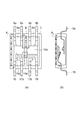
図6は、成型された内部モールド9aおよび内部モールド9bを示す模式図である。図6(a)は平面図、図6(b)は正面図、図6(c)は、Vc−Vc線に沿った断面図である。
FIG. 6 is a schematic diagram showing the molded
図6(a)〜図6(c)に示すように、内部モールド9aからリード5a、6a、15および17aが延出し、内部モールド9bからリード5b、6b、17bおよび19が延出する。そして、内部モールド9aと内部モールド9bとの間には、薄膜9cに覆われた接続部15cと接続部19aとが介在する。さらに、ランナー49a、スルーゲート49bの内部に充填されたランナー部樹脂49c、スルーゲート部樹脂49dが形成される。
As shown in FIGS. 6A to 6C, leads 5a, 6a, 15 and 17a extend from the
次に、内部モールド9aおよび9bの周り、および。それらの間に形成された第1の樹脂を取り除く。例えば、内部モールド9aおよび9bの外形に合わせたパンチング刃を用いた打ち抜き加工より、ランナー49aおよびスルーゲート49bの部分に形成されたランナー部樹脂49cおよびスルーゲート部樹脂49d、さらに、成型時に生じたバリ等を除去する。これにより、内部モールド9aと内部モールド9bとの間において、接続部15cおよび19a覆う薄膜9cを残して、余分な樹脂を除去することができる。
Next, around the
次に、図7(a)および(b)に示す成型過程により、内部モールド9aと、内部モールド9bと、薄膜9cに覆われた接続部15cおよび19aと、を覆う外部モールド3を成型する。
Next, the
図7(a)に示すように、内部モールド9aおよび9bが形成されたリードフレーム20および30を下金型62にセットする。続いて、上金型61と下金型62とを型締めし、キャビティ63を形成する。
As shown in FIG. 7A, the lead frames 20 and 30 on which the
次に、キャビティ63に連通するランナー65を介して、溶融した第2の樹脂を注入する。そして、キャビティ63の内部に充填された樹脂を硬化させ、内部モールド9aおよび9bと、薄膜9cと、を覆う外部モールド3を成型する。続いて、外部モールド3が成型されたリードフレーム20および30を金型から取り出し、共通フレーム31および33を切断して個別の半導体装置100に分離する。
Next, molten second resin is injected through a
上記の製造過程において、第1の樹脂として、例えば、硬質のエポキシ樹脂を用いることにより、薄膜9cに覆われた接続部15cおよび19aの強度を向上させることができる。これにより、内部モールド9aおよび9bを成型したリードフレーム20および30の変形を抑制し、半導体装置100の品質および製造歩留りを向上させることができる。
In the above manufacturing process, the strength of the connecting
以上、本発明のいくつかの実施形態を説明したが、これらの実施形態は、例として提示したものであり、発明の範囲を限定することは意図していない。これら新規な実施形態は、その他の様々な形態で実施されることが可能であり、発明の要旨を逸脱しない範囲で、種々の省略、置き換え、変更を行うことができる。これら実施形態やその変形は、発明の範囲や要旨に含まれるとともに、特許請求の範囲に記載された発明とその均等の範囲に含まれる。 As mentioned above, although some embodiment of this invention was described, these embodiment is shown as an example and is not intending limiting the range of invention. These novel embodiments can be implemented in various other forms, and various omissions, replacements, and changes can be made without departing from the scope of the invention. These embodiments and modifications thereof are included in the scope and gist of the invention, and are included in the invention described in the claims and the equivalents thereof.
3・・・外部モールド、 3a・・・遮蔽部、 5、5a、5b、6a、6b、15、17a、17b、19・・・リード、 5c、5d、15a、15b・・・マウント部、 7、7a、7b・・・発光素子、 7c・・・発光面、 9、9a、9b・・・内部モールド、 9c・・・薄膜、 10・・・樹脂パッケージ、 13、13a、13b・・・受光素子、 13c・・・受光面、 13e・・・電源端子、 13f・・・信号端子、 13g・・・接地端子、 15c、19a・・・接続部、 20、30・・・リードフレーム、 21a、21b、22a、22b、23a、23b、24a、24b・・・ワイヤ、 31、33・・・共通フレーム、 41、61・・・上金型、 42、62・・・下金型、 43、45、63・・・キャビティ、 47・・・ギャップ、 49a、65・・・ランナー、 49b・・・スルーゲート、 49c・・・ランナー部樹脂、 49d・・・スルーゲート部樹脂、 100・・・半導体装置 3 ... External mold, 3a ... Shielding part, 5, 5a, 5b, 6a, 6b, 15, 17a, 17b, 19 ... Lead, 5c, 5d, 15a, 15b ... Mounting part, 7 , 7a, 7b ... light emitting element, 7c ... light emitting surface, 9, 9a, 9b ... internal mold, 9c ... thin film, 10 ... resin package, 13, 13a, 13b ... light receiving Element, 13c ... Light receiving surface, 13e ... Power supply terminal, 13f ... Signal terminal, 13g ... Ground terminal, 15c, 19a ... Connection part, 20, 30 ... Lead frame, 21a, 21b, 22a, 22b, 23a, 23b, 24a, 24b ... wire, 31,33 ... common frame, 41,61 ... upper die, 42,62 ... lower die, 43,45 63 ... Cabi T, 47 ... Gap, 49a, 65 ... Runner, 49b ... Through gate, 49c ... Runner part resin, 49d ... Through gate part resin, 100 ... Semiconductor device
Claims (3)
第1のマウント部と、前記第1のマウント部に固着された第1の受光素子と、第2のマウント部と、前記第2のマウント部に固着された第2の受光素子と、前記第1のマウント部を前記第2のマウント部に接続する接続部と、を有する第2のフレームと、を準備する工程と、
第1のキャビティと、第2のキャビティと、前記第2のキャビティに連通するランナーと、前記第2のキャビティから前記第1のキャビティに連通するスルーゲートおよびギャップと、を有する金型に、前記第1のフレームと、前記第2のフレームと、をセットし樹脂成型する成型工程であって、
前記第1の発光素子が固着された前記第1のリードと、前記第1の受光素子が固着された前記第1のマウント部と、を前記第1のキャビティに収容し、
前記第2の発光素子が固着された前記第2のリードと、前記第2の受光素子が固着された前記第2のマウント部と、を前記第2のキャビティに収容し、
前記接続部を前記ギャップに収容し、
前記ランナーおよび前記スルーゲートを介して、前記第1のキャビティと、前記第2のキャビティと、前記ギャップと、に第1の樹脂を充填し、前記第1のキャビティに第1の成型部、および、前記第2のキャビティに第2の成型部を形成する成型工程と、
前記ギャップ内に充填され、前記接続部を覆う前記第1の樹脂を残し、前記ランナー内に充填され、前記第2の成型部につながった前記第1の樹脂と、前記スルーゲート内に充填され、前記第1の成型部および前記第2の成型部につながった前記第1の樹脂を除去する工程と、
前記第1の成型部と、前記第2の成型部と、前記第1の樹脂からなる薄膜に覆われた前記接続部と、を覆う第2の樹脂からなる第3の成型部を形成する工程と、
を備えた半導体装置の製造方法。 First lead in which the first light-emitting element is fixed, and a second lead second light emitting element is fixed, a first frame having a
A first mount portion; a first light receiving element fixed to the first mount portion; a second mount portion; a second light receiving element fixed to the second mount portion; Preparing a second frame having a connection portion for connecting one mount portion to the second mount portion;
A first cavity, a second cavity, and a runner communicating with the second cavity, the mold having a through gates and gaps, the communication with the first cavity from the second cavity, the A molding step in which a first frame and the second frame are set and resin-molded;
Housing said first light emitting element is secured to said first lead, said first light receiving element secured to said first mounting portion, the said first cavity,
Accommodating a said second light emitting element is fixed a second lead, and the second light receiving element is secured to said second mount portion, the said second cavity,
Accommodating the connecting portion in the gap;
Via the runner and the through gate, the first cavity, the second cavity, and the gap are filled with a first resin, the first cavity is filled with a first molding part, and A molding step of forming a second molding portion in the second cavity;
The first resin filled in the gap and covering the connecting portion , leaving the first resin filled in the runner and connected to the second molded portion, and filled in the through gate. Removing the first resin connected to the first molding part and the second molding part;
Forming a third molded part made of a second resin that covers the first molded part, the second molded part, and the connecting part covered with the thin film made of the first resin; When,
A method for manufacturing a semiconductor device comprising:
前記第1の受光素子および前記第2の受光素子に電気的に接続されたリードは、前記接続部と共に前記ギャップに収容され、前記第1の樹脂からなる薄膜に覆われる請求項1または2に記載の半導体装置の製造方法。 It said second frame further comprises an electrically connected rie de to said first light receiving element and the second light receiving element,
The lead electrically connected to the first light receiving element and the second light receiving element is accommodated in the gap together with the connecting portion , and is covered with a thin film made of the first resin. The manufacturing method of the semiconductor device of description.
Priority Applications (5)
| Application Number | Priority Date | Filing Date | Title |
|---|---|---|---|
| JP2011224285A JP5649547B2 (en) | 2011-10-11 | 2011-10-11 | Manufacturing method of semiconductor device |
| US13/425,232 US20130087811A1 (en) | 2011-10-11 | 2012-03-20 | Semiconductor device and method for manufacturing the same |
| US14/320,366 US9059368B2 (en) | 2011-10-11 | 2014-06-30 | Semiconductor device and method for manufacturing the same |
| US14/709,162 US20150243828A1 (en) | 2011-10-11 | 2015-05-11 | Semiconductor device and method for manufacturing the same |
| US14/857,288 US9472536B2 (en) | 2011-10-11 | 2015-09-17 | Semiconductor device and method for manufacturing the same |
Applications Claiming Priority (1)
| Application Number | Priority Date | Filing Date | Title |
|---|---|---|---|
| JP2011224285A JP5649547B2 (en) | 2011-10-11 | 2011-10-11 | Manufacturing method of semiconductor device |
Publications (2)
| Publication Number | Publication Date |
|---|---|
| JP2013084813A JP2013084813A (en) | 2013-05-09 |
| JP5649547B2 true JP5649547B2 (en) | 2015-01-07 |
Family
ID=48041514
Family Applications (1)
| Application Number | Title | Priority Date | Filing Date |
|---|---|---|---|
| JP2011224285A Active JP5649547B2 (en) | 2011-10-11 | 2011-10-11 | Manufacturing method of semiconductor device |
Country Status (2)
| Country | Link |
|---|---|
| US (3) | US20130087811A1 (en) |
| JP (1) | JP5649547B2 (en) |
Families Citing this family (4)
| Publication number | Priority date | Publication date | Assignee | Title |
|---|---|---|---|---|
| JP2013197302A (en) * | 2012-03-19 | 2013-09-30 | Toshiba Corp | Semiconductor device and manufacturing method therefor |
| EP3121853B1 (en) * | 2015-07-23 | 2022-01-19 | ams AG | Method of producing an optical sensor at wafer-level and optical sensor |
| JP6445940B2 (en) * | 2015-08-03 | 2018-12-26 | 株式会社東芝 | Optical coupling device |
| JP6445947B2 (en) * | 2015-09-04 | 2018-12-26 | 株式会社東芝 | Optical coupling device |
Family Cites Families (11)
| Publication number | Priority date | Publication date | Assignee | Title |
|---|---|---|---|---|
| US4047045A (en) * | 1975-03-03 | 1977-09-06 | Paxton Jr Grady W | Optical coupler |
| JPH0648883Y2 (en) * | 1987-09-30 | 1994-12-12 | シャープ株式会社 | Optical coupling element |
| JP3676136B2 (en) * | 1999-08-23 | 2005-07-27 | シャープ株式会社 | Optical coupling element |
| JP4117868B2 (en) * | 1999-11-22 | 2008-07-16 | シャープ株式会社 | Optical coupling element |
| JP3748380B2 (en) * | 2001-02-08 | 2006-02-22 | シャープ株式会社 | Manufacturing method of multi-channel optical coupling device |
| JP2008028033A (en) * | 2006-07-19 | 2008-02-07 | Sharp Corp | Optical coupling apparatus and electronic apparatus |
| JP4219954B2 (en) * | 2006-12-28 | 2009-02-04 | シャープ株式会社 | MULTICHANNEL OPTICAL COUPLING DEVICE, ELECTRONIC DEVICE, LEAD FRAME MEMBER AND MULTICHANNEL OPTICAL COUPLING MANUFACTURING METHOD |
| JP2010161202A (en) * | 2009-01-08 | 2010-07-22 | Renesas Electronics Corp | Optically coupled device and method of manufacturing the same |
| US7973393B2 (en) * | 2009-02-04 | 2011-07-05 | Fairchild Semiconductor Corporation | Stacked micro optocouplers and methods of making the same |
| JP5381280B2 (en) * | 2009-04-23 | 2014-01-08 | オムロン株式会社 | Optical coupling device |
| JP2013197302A (en) * | 2012-03-19 | 2013-09-30 | Toshiba Corp | Semiconductor device and manufacturing method therefor |
-
2011
- 2011-10-11 JP JP2011224285A patent/JP5649547B2/en active Active
-
2012
- 2012-03-20 US US13/425,232 patent/US20130087811A1/en not_active Abandoned
-
2014
- 2014-06-30 US US14/320,366 patent/US9059368B2/en active Active
-
2015
- 2015-05-11 US US14/709,162 patent/US20150243828A1/en not_active Abandoned
Also Published As
| Publication number | Publication date |
|---|---|
| US9059368B2 (en) | 2015-06-16 |
| US20150243828A1 (en) | 2015-08-27 |
| JP2013084813A (en) | 2013-05-09 |
| US20130087811A1 (en) | 2013-04-11 |
| US20140315337A1 (en) | 2014-10-23 |
Similar Documents
| Publication | Publication Date | Title |
|---|---|---|
| JP4952233B2 (en) | Semiconductor device | |
| JP5802695B2 (en) | Semiconductor device and method for manufacturing semiconductor device | |
| JP5649547B2 (en) | Manufacturing method of semiconductor device | |
| KR100899554B1 (en) | Light emitting diode package and its manufacturing method | |
| TWI531089B (en) | Light-emitting diode package structure and manufacturing method thereof | |
| JP2020088091A (en) | Optical coupling device | |
| JP2010114141A (en) | Light reception/light emission integrated type semiconductor device, and electronic equipment | |
| JP5908294B2 (en) | Semiconductor device and manufacturing method thereof | |
| JP2017034127A (en) | Optical coupling device | |
| JP4117868B2 (en) | Optical coupling element | |
| US9472536B2 (en) | Semiconductor device and method for manufacturing the same | |
| US8624286B2 (en) | Semiconductor device | |
| JP2007067414A (en) | Double mold optical coupler | |
| US8334175B1 (en) | Manufacturing method of LED package structure | |
| KR100650463B1 (en) | Semiconductor device and manufacturing method thereof | |
| JP2013065717A (en) | Semiconductor device and manufacturing method of the same | |
| KR200470928Y1 (en) | Photo coupler | |
| JP2704321B2 (en) | Method for manufacturing optical semiconductor device | |
| JP2007173562A (en) | Optical semiconductor device and electronic device having same | |
| KR20130098461A (en) | Light emitting diode package and method of manufacturing the same | |
| JP7319088B2 (en) | light receiving and emitting device | |
| CN112436002A (en) | Multichannel optical coupler and manufacturing method thereof | |
| CN105870211B (en) | A kind of optical sensor package structure and its manufacture method | |
| JP3710522B2 (en) | Optical semiconductor device and manufacturing method thereof | |
| CN215644404U (en) | Power module's packaging mold and power module |
Legal Events
| Date | Code | Title | Description |
|---|---|---|---|
| A621 | Written request for application examination |
Free format text: JAPANESE INTERMEDIATE CODE: A621 Effective date: 20140204 |
|
| A131 | Notification of reasons for refusal |
Free format text: JAPANESE INTERMEDIATE CODE: A131 Effective date: 20140417 |
|
| A521 | Request for written amendment filed |
Free format text: JAPANESE INTERMEDIATE CODE: A523 Effective date: 20140616 |
|
| A131 | Notification of reasons for refusal |
Free format text: JAPANESE INTERMEDIATE CODE: A131 Effective date: 20140819 |
|
| A521 | Request for written amendment filed |
Free format text: JAPANESE INTERMEDIATE CODE: A523 Effective date: 20140926 |
|
| TRDD | Decision of grant or rejection written | ||
| A01 | Written decision to grant a patent or to grant a registration (utility model) |
Free format text: JAPANESE INTERMEDIATE CODE: A01 Effective date: 20141015 |
|
| A61 | First payment of annual fees (during grant procedure) |
Free format text: JAPANESE INTERMEDIATE CODE: A61 Effective date: 20141111 |
|
| R151 | Written notification of patent or utility model registration |
Ref document number: 5649547 Country of ref document: JP Free format text: JAPANESE INTERMEDIATE CODE: R151 |