JP5621964B2 - Liquid ejecting head, liquid ejecting apparatus, piezoelectric element, and ultrasonic device - Google Patents
Liquid ejecting head, liquid ejecting apparatus, piezoelectric element, and ultrasonic device Download PDFInfo
- Publication number
- JP5621964B2 JP5621964B2 JP2010115744A JP2010115744A JP5621964B2 JP 5621964 B2 JP5621964 B2 JP 5621964B2 JP 2010115744 A JP2010115744 A JP 2010115744A JP 2010115744 A JP2010115744 A JP 2010115744A JP 5621964 B2 JP5621964 B2 JP 5621964B2
- Authority
- JP
- Japan
- Prior art keywords
- piezoelectric element
- piezoelectric
- phase
- liquid ejecting
- electrode
- Prior art date
- Legal status (The legal status is an assumption and is not a legal conclusion. Google has not performed a legal analysis and makes no representation as to the accuracy of the status listed.)
- Expired - Fee Related
Links
- 239000007788 liquid Substances 0.000 title claims description 33
- 239000000463 material Substances 0.000 claims description 46
- 229910052748 manganese Inorganic materials 0.000 claims description 23
- 230000001747 exhibiting effect Effects 0.000 claims description 21
- 230000005621 ferroelectricity Effects 0.000 claims description 13
- 238000000634 powder X-ray diffraction Methods 0.000 claims description 9
- 230000005620 antiferroelectricity Effects 0.000 claims description 7
- 239000000758 substrate Substances 0.000 description 44
- XEEYBQQBJWHFJM-UHFFFAOYSA-N iron Substances [Fe] XEEYBQQBJWHFJM-UHFFFAOYSA-N 0.000 description 28
- 230000000052 comparative effect Effects 0.000 description 24
- 239000011572 manganese Substances 0.000 description 22
- 238000010586 diagram Methods 0.000 description 20
- 230000005684 electric field Effects 0.000 description 20
- 238000000034 method Methods 0.000 description 18
- 229910052797 bismuth Inorganic materials 0.000 description 15
- 229910052742 iron Inorganic materials 0.000 description 15
- 229910052746 lanthanum Inorganic materials 0.000 description 15
- VYPSYNLAJGMNEJ-UHFFFAOYSA-N Silicium dioxide Chemical compound O=[Si]=O VYPSYNLAJGMNEJ-UHFFFAOYSA-N 0.000 description 14
- 239000000203 mixture Substances 0.000 description 14
- BASFCYQUMIYNBI-UHFFFAOYSA-N platinum Chemical compound [Pt] BASFCYQUMIYNBI-UHFFFAOYSA-N 0.000 description 14
- 239000012212 insulator Substances 0.000 description 12
- 230000010287 polarization Effects 0.000 description 12
- 230000007704 transition Effects 0.000 description 12
- 239000002131 composite material Substances 0.000 description 11
- 238000004891 communication Methods 0.000 description 10
- 239000002243 precursor Substances 0.000 description 10
- 230000001681 protective effect Effects 0.000 description 10
- 238000005238 degreasing Methods 0.000 description 9
- 150000002902 organometallic compounds Chemical class 0.000 description 9
- 238000001035 drying Methods 0.000 description 8
- 230000008569 process Effects 0.000 description 8
- XUIMIQQOPSSXEZ-UHFFFAOYSA-N Silicon Chemical compound [Si] XUIMIQQOPSSXEZ-UHFFFAOYSA-N 0.000 description 7
- 229910052710 silicon Inorganic materials 0.000 description 7
- 239000010703 silicon Substances 0.000 description 7
- 235000012239 silicon dioxide Nutrition 0.000 description 7
- 239000000377 silicon dioxide Substances 0.000 description 7
- 238000012360 testing method Methods 0.000 description 7
- GWEVSGVZZGPLCZ-UHFFFAOYSA-N Titan oxide Chemical compound O=[Ti]=O GWEVSGVZZGPLCZ-UHFFFAOYSA-N 0.000 description 6
- 238000000576 coating method Methods 0.000 description 6
- 238000006073 displacement reaction Methods 0.000 description 6
- 229910052451 lead zirconate titanate Inorganic materials 0.000 description 6
- 229910052697 platinum Inorganic materials 0.000 description 6
- OGIDPMRJRNCKJF-UHFFFAOYSA-N titanium oxide Inorganic materials [Ti]=O OGIDPMRJRNCKJF-UHFFFAOYSA-N 0.000 description 6
- 229910052751 metal Inorganic materials 0.000 description 5
- 239000002184 metal Substances 0.000 description 5
- 238000004151 rapid thermal annealing Methods 0.000 description 5
- 238000004544 sputter deposition Methods 0.000 description 5
- 239000000126 substance Substances 0.000 description 5
- 238000002441 X-ray diffraction Methods 0.000 description 4
- JCXGWMGPZLAOME-UHFFFAOYSA-N bismuth atom Chemical compound [Bi] JCXGWMGPZLAOME-UHFFFAOYSA-N 0.000 description 4
- 239000013078 crystal Substances 0.000 description 4
- 238000010304 firing Methods 0.000 description 4
- FZLIPJUXYLNCLC-UHFFFAOYSA-N lanthanum atom Chemical compound [La] FZLIPJUXYLNCLC-UHFFFAOYSA-N 0.000 description 4
- 238000004519 manufacturing process Methods 0.000 description 4
- 238000007789 sealing Methods 0.000 description 4
- SMSVUYQRWYTTLI-UHFFFAOYSA-L 2-ethylhexanoate;iron(2+) Chemical compound [Fe+2].CCCCC(CC)C([O-])=O.CCCCC(CC)C([O-])=O SMSVUYQRWYTTLI-UHFFFAOYSA-L 0.000 description 3
- PPNFILUQDVDXDA-UHFFFAOYSA-K 2-ethylhexanoate;lanthanum(3+) Chemical compound [La+3].CCCCC(CC)C([O-])=O.CCCCC(CC)C([O-])=O.CCCCC(CC)C([O-])=O PPNFILUQDVDXDA-UHFFFAOYSA-K 0.000 description 3
- FHRAKXJVEOBCBQ-UHFFFAOYSA-L 2-ethylhexanoate;manganese(2+) Chemical compound [Mn+2].CCCCC(CC)C([O-])=O.CCCCC(CC)C([O-])=O FHRAKXJVEOBCBQ-UHFFFAOYSA-L 0.000 description 3
- PWHULOQIROXLJO-UHFFFAOYSA-N Manganese Chemical compound [Mn] PWHULOQIROXLJO-UHFFFAOYSA-N 0.000 description 3
- NUMHJBONQMZPBW-UHFFFAOYSA-K bis(2-ethylhexanoyloxy)bismuthanyl 2-ethylhexanoate Chemical compound [Bi+3].CCCCC(CC)C([O-])=O.CCCCC(CC)C([O-])=O.CCCCC(CC)C([O-])=O NUMHJBONQMZPBW-UHFFFAOYSA-K 0.000 description 3
- 230000006870 function Effects 0.000 description 3
- 238000010438 heat treatment Methods 0.000 description 3
- 238000002156 mixing Methods 0.000 description 3
- 230000003647 oxidation Effects 0.000 description 3
- 238000007254 oxidation reaction Methods 0.000 description 3
- RVTZCBVAJQQJTK-UHFFFAOYSA-N oxygen(2-);zirconium(4+) Chemical compound [O-2].[O-2].[Zr+4] RVTZCBVAJQQJTK-UHFFFAOYSA-N 0.000 description 3
- 229910001928 zirconium oxide Inorganic materials 0.000 description 3
- CTQNGGLPUBDAKN-UHFFFAOYSA-N O-Xylene Chemical compound CC1=CC=CC=C1C CTQNGGLPUBDAKN-UHFFFAOYSA-N 0.000 description 2
- RTAQQCXQSZGOHL-UHFFFAOYSA-N Titanium Chemical compound [Ti] RTAQQCXQSZGOHL-UHFFFAOYSA-N 0.000 description 2
- 239000000853 adhesive Substances 0.000 description 2
- 230000001070 adhesive effect Effects 0.000 description 2
- 238000000137 annealing Methods 0.000 description 2
- QVGXLLKOCUKJST-UHFFFAOYSA-N atomic oxygen Chemical compound [O] QVGXLLKOCUKJST-UHFFFAOYSA-N 0.000 description 2
- 230000008859 change Effects 0.000 description 2
- 238000000151 deposition Methods 0.000 description 2
- 230000007613 environmental effect Effects 0.000 description 2
- 239000011521 glass Substances 0.000 description 2
- 239000010931 gold Substances 0.000 description 2
- HFGPZNIAWCZYJU-UHFFFAOYSA-N lead zirconate titanate Chemical group [O-2].[O-2].[O-2].[O-2].[O-2].[Ti+4].[Zr+4].[Pb+2] HFGPZNIAWCZYJU-UHFFFAOYSA-N 0.000 description 2
- TVMXDCGIABBOFY-UHFFFAOYSA-N octane Chemical compound CCCCCCCC TVMXDCGIABBOFY-UHFFFAOYSA-N 0.000 description 2
- 229910052760 oxygen Inorganic materials 0.000 description 2
- 239000001301 oxygen Substances 0.000 description 2
- 230000004044 response Effects 0.000 description 2
- 238000004528 spin coating Methods 0.000 description 2
- 239000010936 titanium Substances 0.000 description 2
- 229910052719 titanium Inorganic materials 0.000 description 2
- 239000008096 xylene Substances 0.000 description 2
- WKBPZYKAUNRMKP-UHFFFAOYSA-N 1-[2-(2,4-dichlorophenyl)pentyl]1,2,4-triazole Chemical compound C=1C=C(Cl)C=C(Cl)C=1C(CCC)CN1C=NC=N1 WKBPZYKAUNRMKP-UHFFFAOYSA-N 0.000 description 1
- 238000000018 DNA microarray Methods 0.000 description 1
- LFQSCWFLJHTTHZ-UHFFFAOYSA-N Ethanol Chemical compound CCO LFQSCWFLJHTTHZ-UHFFFAOYSA-N 0.000 description 1
- 229910004298 SiO 2 Inorganic materials 0.000 description 1
- 239000000443 aerosol Substances 0.000 description 1
- 150000004703 alkoxides Chemical class 0.000 description 1
- 238000013459 approach Methods 0.000 description 1
- 238000005452 bending Methods 0.000 description 1
- 230000015572 biosynthetic process Effects 0.000 description 1
- 230000015556 catabolic process Effects 0.000 description 1
- 229910010293 ceramic material Inorganic materials 0.000 description 1
- 238000006243 chemical reaction Methods 0.000 description 1
- 238000005229 chemical vapour deposition Methods 0.000 description 1
- 238000000354 decomposition reaction Methods 0.000 description 1
- 239000003989 dielectric material Substances 0.000 description 1
- 239000007772 electrode material Substances 0.000 description 1
- 239000002241 glass-ceramic Substances 0.000 description 1
- PCHJSUWPFVWCPO-UHFFFAOYSA-N gold Chemical compound [Au] PCHJSUWPFVWCPO-UHFFFAOYSA-N 0.000 description 1
- 229910052737 gold Inorganic materials 0.000 description 1
- 238000009413 insulation Methods 0.000 description 1
- 150000002500 ions Chemical class 0.000 description 1
- 229910052741 iridium Inorganic materials 0.000 description 1
- GKOZUEZYRPOHIO-UHFFFAOYSA-N iridium atom Chemical compound [Ir] GKOZUEZYRPOHIO-UHFFFAOYSA-N 0.000 description 1
- 238000000608 laser ablation Methods 0.000 description 1
- 239000004973 liquid crystal related substance Substances 0.000 description 1
- 238000001459 lithography Methods 0.000 description 1
- WPBNNNQJVZRUHP-UHFFFAOYSA-L manganese(2+);methyl n-[[2-(methoxycarbonylcarbamothioylamino)phenyl]carbamothioyl]carbamate;n-[2-(sulfidocarbothioylamino)ethyl]carbamodithioate Chemical compound [Mn+2].[S-]C(=S)NCCNC([S-])=S.COC(=O)NC(=S)NC1=CC=CC=C1NC(=S)NC(=O)OC WPBNNNQJVZRUHP-UHFFFAOYSA-L 0.000 description 1
- 238000005259 measurement Methods 0.000 description 1
- 239000012528 membrane Substances 0.000 description 1
- 229910044991 metal oxide Inorganic materials 0.000 description 1
- 150000004706 metal oxides Chemical class 0.000 description 1
- -1 organic acid salts Chemical class 0.000 description 1
- 239000003960 organic solvent Substances 0.000 description 1
- 238000001552 radio frequency sputter deposition Methods 0.000 description 1
- 239000004065 semiconductor Substances 0.000 description 1
- 238000003980 solgel method Methods 0.000 description 1
- 239000002904 solvent Substances 0.000 description 1
- 230000002269 spontaneous effect Effects 0.000 description 1
- 229910001220 stainless steel Inorganic materials 0.000 description 1
- 239000010935 stainless steel Substances 0.000 description 1
- 238000007740 vapor deposition Methods 0.000 description 1
Images


Classifications
-
- C—CHEMISTRY; METALLURGY
- C04—CEMENTS; CONCRETE; ARTIFICIAL STONE; CERAMICS; REFRACTORIES
- C04B—LIME, MAGNESIA; SLAG; CEMENTS; COMPOSITIONS THEREOF, e.g. MORTARS, CONCRETE OR LIKE BUILDING MATERIALS; ARTIFICIAL STONE; CERAMICS; REFRACTORIES; TREATMENT OF NATURAL STONE
- C04B35/00—Shaped ceramic products characterised by their composition; Ceramics compositions; Processing powders of inorganic compounds preparatory to the manufacturing of ceramic products
- C04B35/01—Shaped ceramic products characterised by their composition; Ceramics compositions; Processing powders of inorganic compounds preparatory to the manufacturing of ceramic products based on oxide ceramics
- C04B35/26—Shaped ceramic products characterised by their composition; Ceramics compositions; Processing powders of inorganic compounds preparatory to the manufacturing of ceramic products based on oxide ceramics based on ferrites
- C04B35/2608—Compositions containing one or more ferrites of the group comprising manganese, zinc, nickel, copper or cobalt and one or more ferrites of the group comprising rare earth metals, alkali metals, alkaline earth metals or lead
-
- B—PERFORMING OPERATIONS; TRANSPORTING
- B41—PRINTING; LINING MACHINES; TYPEWRITERS; STAMPS
- B41J—TYPEWRITERS; SELECTIVE PRINTING MECHANISMS, i.e. MECHANISMS PRINTING OTHERWISE THAN FROM A FORME; CORRECTION OF TYPOGRAPHICAL ERRORS
- B41J2/00—Typewriters or selective printing mechanisms characterised by the printing or marking process for which they are designed
- B41J2/005—Typewriters or selective printing mechanisms characterised by the printing or marking process for which they are designed characterised by bringing liquid or particles selectively into contact with a printing material
- B41J2/01—Ink jet
- B41J2/015—Ink jet characterised by the jet generation process
- B41J2/04—Ink jet characterised by the jet generation process generating single droplets or particles on demand
- B41J2/045—Ink jet characterised by the jet generation process generating single droplets or particles on demand by pressure, e.g. electromechanical transducers
- B41J2/055—Devices for absorbing or preventing back-pressure
-
- B—PERFORMING OPERATIONS; TRANSPORTING
- B41—PRINTING; LINING MACHINES; TYPEWRITERS; STAMPS
- B41J—TYPEWRITERS; SELECTIVE PRINTING MECHANISMS, i.e. MECHANISMS PRINTING OTHERWISE THAN FROM A FORME; CORRECTION OF TYPOGRAPHICAL ERRORS
- B41J2/00—Typewriters or selective printing mechanisms characterised by the printing or marking process for which they are designed
- B41J2/005—Typewriters or selective printing mechanisms characterised by the printing or marking process for which they are designed characterised by bringing liquid or particles selectively into contact with a printing material
- B41J2/01—Ink jet
- B41J2/135—Nozzles
- B41J2/14—Structure thereof only for on-demand ink jet heads
- B41J2/14201—Structure of print heads with piezoelectric elements
- B41J2/14233—Structure of print heads with piezoelectric elements of film type, deformed by bending and disposed on a diaphragm
-
- H—ELECTRICITY
- H10—SEMICONDUCTOR DEVICES; ELECTRIC SOLID-STATE DEVICES NOT OTHERWISE PROVIDED FOR
- H10N—ELECTRIC SOLID-STATE DEVICES NOT OTHERWISE PROVIDED FOR
- H10N30/00—Piezoelectric or electrostrictive devices
- H10N30/20—Piezoelectric or electrostrictive devices with electrical input and mechanical output, e.g. functioning as actuators or vibrators
- H10N30/204—Piezoelectric or electrostrictive devices with electrical input and mechanical output, e.g. functioning as actuators or vibrators using bending displacement, e.g. unimorph, bimorph or multimorph cantilever or membrane benders
- H10N30/2047—Membrane type
-
- H—ELECTRICITY
- H10—SEMICONDUCTOR DEVICES; ELECTRIC SOLID-STATE DEVICES NOT OTHERWISE PROVIDED FOR
- H10N—ELECTRIC SOLID-STATE DEVICES NOT OTHERWISE PROVIDED FOR
- H10N30/00—Piezoelectric or electrostrictive devices
- H10N30/80—Constructional details
- H10N30/85—Piezoelectric or electrostrictive active materials
- H10N30/853—Ceramic compositions
- H10N30/8561—Bismuth-based oxides
-
- B—PERFORMING OPERATIONS; TRANSPORTING
- B41—PRINTING; LINING MACHINES; TYPEWRITERS; STAMPS
- B41J—TYPEWRITERS; SELECTIVE PRINTING MECHANISMS, i.e. MECHANISMS PRINTING OTHERWISE THAN FROM A FORME; CORRECTION OF TYPOGRAPHICAL ERRORS
- B41J2/00—Typewriters or selective printing mechanisms characterised by the printing or marking process for which they are designed
- B41J2/005—Typewriters or selective printing mechanisms characterised by the printing or marking process for which they are designed characterised by bringing liquid or particles selectively into contact with a printing material
- B41J2/01—Ink jet
- B41J2/135—Nozzles
- B41J2/14—Structure thereof only for on-demand ink jet heads
- B41J2/14201—Structure of print heads with piezoelectric elements
- B41J2/14233—Structure of print heads with piezoelectric elements of film type, deformed by bending and disposed on a diaphragm
- B41J2002/14241—Structure of print heads with piezoelectric elements of film type, deformed by bending and disposed on a diaphragm having a cover around the piezoelectric thin film element
-
- B—PERFORMING OPERATIONS; TRANSPORTING
- B41—PRINTING; LINING MACHINES; TYPEWRITERS; STAMPS
- B41J—TYPEWRITERS; SELECTIVE PRINTING MECHANISMS, i.e. MECHANISMS PRINTING OTHERWISE THAN FROM A FORME; CORRECTION OF TYPOGRAPHICAL ERRORS
- B41J2202/00—Embodiments of or processes related to ink-jet or thermal heads
- B41J2202/01—Embodiments of or processes related to ink-jet heads
- B41J2202/03—Specific materials used
-
- C—CHEMISTRY; METALLURGY
- C04—CEMENTS; CONCRETE; ARTIFICIAL STONE; CERAMICS; REFRACTORIES
- C04B—LIME, MAGNESIA; SLAG; CEMENTS; COMPOSITIONS THEREOF, e.g. MORTARS, CONCRETE OR LIKE BUILDING MATERIALS; ARTIFICIAL STONE; CERAMICS; REFRACTORIES; TREATMENT OF NATURAL STONE
- C04B2235/00—Aspects relating to ceramic starting mixtures or sintered ceramic products
- C04B2235/02—Composition of constituents of the starting material or of secondary phases of the final product
- C04B2235/30—Constituents and secondary phases not being of a fibrous nature
- C04B2235/32—Metal oxides, mixed metal oxides, or oxide-forming salts thereof, e.g. carbonates, nitrates, (oxy)hydroxides, chlorides
- C04B2235/3224—Rare earth oxide or oxide forming salts thereof, e.g. scandium oxide
- C04B2235/3227—Lanthanum oxide or oxide-forming salts thereof
-
- C—CHEMISTRY; METALLURGY
- C04—CEMENTS; CONCRETE; ARTIFICIAL STONE; CERAMICS; REFRACTORIES
- C04B—LIME, MAGNESIA; SLAG; CEMENTS; COMPOSITIONS THEREOF, e.g. MORTARS, CONCRETE OR LIKE BUILDING MATERIALS; ARTIFICIAL STONE; CERAMICS; REFRACTORIES; TREATMENT OF NATURAL STONE
- C04B2235/00—Aspects relating to ceramic starting mixtures or sintered ceramic products
- C04B2235/02—Composition of constituents of the starting material or of secondary phases of the final product
- C04B2235/30—Constituents and secondary phases not being of a fibrous nature
- C04B2235/32—Metal oxides, mixed metal oxides, or oxide-forming salts thereof, e.g. carbonates, nitrates, (oxy)hydroxides, chlorides
- C04B2235/3262—Manganese oxides, manganates, rhenium oxides or oxide-forming salts thereof, e.g. MnO
-
- C—CHEMISTRY; METALLURGY
- C04—CEMENTS; CONCRETE; ARTIFICIAL STONE; CERAMICS; REFRACTORIES
- C04B—LIME, MAGNESIA; SLAG; CEMENTS; COMPOSITIONS THEREOF, e.g. MORTARS, CONCRETE OR LIKE BUILDING MATERIALS; ARTIFICIAL STONE; CERAMICS; REFRACTORIES; TREATMENT OF NATURAL STONE
- C04B2235/00—Aspects relating to ceramic starting mixtures or sintered ceramic products
- C04B2235/02—Composition of constituents of the starting material or of secondary phases of the final product
- C04B2235/30—Constituents and secondary phases not being of a fibrous nature
- C04B2235/32—Metal oxides, mixed metal oxides, or oxide-forming salts thereof, e.g. carbonates, nitrates, (oxy)hydroxides, chlorides
- C04B2235/3298—Bismuth oxides, bismuthates or oxide forming salts thereof, e.g. zinc bismuthate
-
- C—CHEMISTRY; METALLURGY
- C04—CEMENTS; CONCRETE; ARTIFICIAL STONE; CERAMICS; REFRACTORIES
- C04B—LIME, MAGNESIA; SLAG; CEMENTS; COMPOSITIONS THEREOF, e.g. MORTARS, CONCRETE OR LIKE BUILDING MATERIALS; ARTIFICIAL STONE; CERAMICS; REFRACTORIES; TREATMENT OF NATURAL STONE
- C04B2235/00—Aspects relating to ceramic starting mixtures or sintered ceramic products
- C04B2235/02—Composition of constituents of the starting material or of secondary phases of the final product
- C04B2235/30—Constituents and secondary phases not being of a fibrous nature
- C04B2235/44—Metal salt constituents or additives chosen for the nature of the anions, e.g. hydrides or acetylacetonate
- C04B2235/441—Alkoxides, e.g. methoxide, tert-butoxide
-
- C—CHEMISTRY; METALLURGY
- C04—CEMENTS; CONCRETE; ARTIFICIAL STONE; CERAMICS; REFRACTORIES
- C04B—LIME, MAGNESIA; SLAG; CEMENTS; COMPOSITIONS THEREOF, e.g. MORTARS, CONCRETE OR LIKE BUILDING MATERIALS; ARTIFICIAL STONE; CERAMICS; REFRACTORIES; TREATMENT OF NATURAL STONE
- C04B2235/00—Aspects relating to ceramic starting mixtures or sintered ceramic products
- C04B2235/70—Aspects relating to sintered or melt-casted ceramic products
- C04B2235/74—Physical characteristics
- C04B2235/76—Crystal structural characteristics, e.g. symmetry
- C04B2235/768—Perovskite structure ABO3
-
- H—ELECTRICITY
- H10—SEMICONDUCTOR DEVICES; ELECTRIC SOLID-STATE DEVICES NOT OTHERWISE PROVIDED FOR
- H10N—ELECTRIC SOLID-STATE DEVICES NOT OTHERWISE PROVIDED FOR
- H10N30/00—Piezoelectric or electrostrictive devices
- H10N30/01—Manufacture or treatment
- H10N30/07—Forming of piezoelectric or electrostrictive parts or bodies on an electrical element or another base
- H10N30/074—Forming of piezoelectric or electrostrictive parts or bodies on an electrical element or another base by depositing piezoelectric or electrostrictive layers, e.g. aerosol or screen printing
- H10N30/077—Forming of piezoelectric or electrostrictive parts or bodies on an electrical element or another base by depositing piezoelectric or electrostrictive layers, e.g. aerosol or screen printing by liquid phase deposition
- H10N30/078—Forming of piezoelectric or electrostrictive parts or bodies on an electrical element or another base by depositing piezoelectric or electrostrictive layers, e.g. aerosol or screen printing by liquid phase deposition by sol-gel deposition
Landscapes
- Engineering & Computer Science (AREA)
- Chemical & Material Sciences (AREA)
- Ceramic Engineering (AREA)
- Manufacturing & Machinery (AREA)
- Materials Engineering (AREA)
- Structural Engineering (AREA)
- Organic Chemistry (AREA)
- Particle Formation And Scattering Control In Inkjet Printers (AREA)
- Compositions Of Oxide Ceramics (AREA)
- Coating Apparatus (AREA)
Description
本発明は、ノズル開口に連通する圧力発生室に圧力変化を生じさせる第1電極、圧電体層及び第2電極からなる圧電素子を具備する液体噴射ヘッド、液体噴射装置及び圧電素子並びに超音波デバイスに関する。 The present invention relates to a liquid ejecting head, a liquid ejecting apparatus, a piezoelectric element, and an ultrasonic device including a piezoelectric element including a first electrode, a piezoelectric layer, and a second electrode that cause a pressure change in a pressure generating chamber communicating with a nozzle opening. About.
液体噴射ヘッドに用いられる圧電素子としては、電気的機械変換機能を呈する圧電材料、例えば、結晶化した誘電材料からなる圧電体層を、2つの電極で挟んで構成されたものがある。このような圧電素子は、例えば撓み振動モードのアクチュエーター装置として液体噴射ヘッドに搭載される。液体噴射ヘッドの代表例としては、例えば、インク滴を吐出するノズル開口と連通する圧力発生室の一部を振動板で構成し、この振動板を圧電素子により変形させて圧力発生室のインクを加圧してノズル開口からインク滴として吐出させるインクジェット式記録ヘッドがある。このようなインクジェット式記録ヘッドに搭載される圧電素子は、例えば、振動板の表面全体に亘って成膜技術により均一な圧電材料層を形成し、この圧電材料層をリソグラフィー法により圧力発生室に対応する形状に切り分けて圧力発生室毎に独立するように圧電素子を形成したものがある。 As a piezoelectric element used in a liquid ejecting head, there is a piezoelectric material that exhibits an electromechanical conversion function, for example, a piezoelectric layer made of a crystallized dielectric material and sandwiched between two electrodes. Such a piezoelectric element is mounted on the liquid ejecting head as an actuator device in a flexural vibration mode, for example. As a typical example of a liquid ejecting head, for example, a part of a pressure generation chamber communicating with a nozzle opening for ejecting ink droplets is configured by a vibration plate, and the vibration plate is deformed by a piezoelectric element so that the ink in the pressure generation chamber is There is an ink jet recording head that pressurizes and ejects ink droplets from nozzle openings. In the piezoelectric element mounted on such an ink jet recording head, for example, a uniform piezoelectric material layer is formed over the entire surface of the diaphragm by a film forming technique, and this piezoelectric material layer is formed into a pressure generating chamber by a lithography method. There is one in which piezoelectric elements are formed so as to be separated into corresponding shapes and independent for each pressure generating chamber.
このような圧電素子に用いられる圧電材料には高い圧電特性(歪み量)が求められており、代表例として、チタン酸ジルコン酸鉛(PZT)が挙げられる(特許文献1参照)。このPZTは強誘電体であり、分極方向を一方向に揃えることで歪み量が印加電圧に対して直線的に変化する。したがって、歪み量の制御が容易になるため、吐出させる液滴サイズ等も容易になり、アクチュエーター装置として好適である。 A piezoelectric material used for such a piezoelectric element is required to have high piezoelectric characteristics (distortion amount), and a typical example is lead zirconate titanate (PZT) (see Patent Document 1). This PZT is a ferroelectric, and the amount of strain changes linearly with respect to the applied voltage by aligning the polarization direction in one direction. Therefore, since the control of the amount of distortion becomes easy, the size of the ejected droplets and the like become easy, which is suitable as an actuator device.
しかしながら、前述したチタン酸ジルコン酸鉛には鉛が含まれており、環境問題の観点から、鉛の含有量を抑えた圧電材料が求められている。なお、このような問題はインクジェット式記録ヘッドに代表される液体噴射ヘッドに限定されず、他の圧電素子においても同様に存在する。 However, the above-mentioned lead zirconate titanate contains lead, and from the viewpoint of environmental problems, there is a demand for a piezoelectric material with a reduced lead content. Such a problem is not limited to a liquid jet head typified by an ink jet recording head, and similarly exists in other piezoelectric elements.
本発明はこのような事情に鑑み、環境負荷が小さく、強誘電体からなる圧電素子を有する液体噴射ヘッド、液体噴射装置及び圧電素子並びに超音波デバイスを提供することを目的とする。 In view of such circumstances, an object of the present invention is to provide a liquid ejecting head, a liquid ejecting apparatus, a piezoelectric element, and an ultrasonic device having a piezoelectric element made of a ferroelectric material with a small environmental load.
上記課題を解決する本発明の態様は、下記一般式で表されるペロブスカイト型複合酸化物からなり、粉末X線回折パターンにおいて、強誘電性を示す相に帰属される回折ピークと、反強誘電性を示す相に帰属される回折ピークが同時に観測されることを特徴とする圧電材料にある。
(Bi 1-x ,La x )(Fe 1-y ,Mn y )O 3
(0.17≦x≦0.20,0.01≦y≦0.09)
かかる態様では、反強誘電相と強誘電相を同時に示すため、歪み量の大きな圧電素子とすることができる。また、鉛の含有量を抑えられるため環境への負荷を低減でき、且つ歪み量の制御が容易な圧電材料を提供することができる。
ここで、粉末X線回折パターンにおいて45<2θ<50°にABO3型構造由来の回折ピークが観測され、前記ABO3型構造由来の回折ピークにおける強誘電性を示す相に帰属される回折ピークの面積強度AFと反強誘電性を示す相に帰属される回折ピークの面積強度AAFとの比AAF/AFが、0.1以上であることが好ましい。これによれば、より確実に歪み量の大きな圧電素子とすることができる。
本発明の他の態様は、上述した態様の圧電材料からなる圧電体層と、前記圧電体層に設けられた複数の電極と、を具備することを特徴とする圧電素子にある。
かかる態様では、反強誘電相と強誘電相を同時に示すため、歪み量の大きな圧電素子とすることができる。
また、本発明の他の態様は、上述した態様の圧電素子を備えることを特徴とする液体噴射ヘッドにある。かかる態様では、歪み量の大きな圧電素子を具備する液体噴射ヘッドを実現できる。
また、本発明の他の態様は、上述した態様の圧電素子を備えることを特徴とする液体噴射装置にある。かかる態様では、歪み量の大きな圧電素子を具備する液体噴射装置を実現できる。
また、本発明の他の態様は、上述した態様の圧電素子を備えることを特徴とする超音波デバイスにある。かかる態様では、歪み量の大きな圧電素子を具備する超音波デバイスを実現できる。
さらに、本発明は、以下に示す態様を包含する。
かかる態様は、ノズル開口に連通する圧力発生室と、第1電極と、前記第1電極上に形成された圧電体層と、前記圧電体層上に形成された第2電極と、を備えた圧電素子と、を具備し、前記圧電体層は、Bi、La、Fe及びMnを含むペロブスカイト型複合酸化物からなり、強誘電体であることを特徴とする液体噴射ヘッドにある。
かかる態様では、Bi、La、Fe及びMnを含むペロブスカイト型複合酸化物であって、強誘電体である圧電材料を用いることにより、鉛の含有量を抑えられるため環境への負荷を低減でき、歪み量の制御が容易となり、例えば、吐出する液滴サイズの制御が容易な圧電素子を有する液体噴射ヘッドとすることができる。
An aspect of the present invention that solves the above problems comprises a perovskite complex oxide represented by the following general formula, and in a powder X-ray diffraction pattern, a diffraction peak attributed to a phase exhibiting ferroelectricity, and an antiferroelectric The piezoelectric material is characterized in that diffraction peaks attributed to phases exhibiting properties are observed simultaneously.
(Bi 1-x, La x ) (Fe 1-y, Mn y) O 3
(0.17 ≦ x ≦ 0.20, 0.01 ≦ y ≦ 0.09)
In this aspect, since the antiferroelectric phase and the ferroelectric phase are simultaneously shown, a piezoelectric element having a large strain can be obtained. In addition, since the lead content can be suppressed, it is possible to provide a piezoelectric material that can reduce the load on the environment and can easily control the amount of strain.
Here, in the powder X-ray diffraction pattern, a diffraction peak derived from the ABO 3 type structure is observed at 45 <2θ <50 °, and the diffraction peak attributed to the phase exhibiting ferroelectricity in the diffraction peak derived from the ABO 3 type structure. It is preferable that the ratio A AF / A F of the area intensity A F and the area intensity A AF of the diffraction peak attributed to the antiferroelectric phase is 0.1 or more. According to this, Ru can be a large piezoelectric element more reliably strain.
Another aspect of the present invention is a piezoelectric element comprising: a piezoelectric layer made of the piezoelectric material according to the above-described aspect; and a plurality of electrodes provided on the piezoelectric layer.
In this aspect, since the antiferroelectric phase and the ferroelectric phase are simultaneously shown, a piezoelectric element having a large strain can be obtained.
According to another aspect of the invention, there is provided a liquid ejecting head including the piezoelectric element according to the aspect described above. In this aspect, a liquid jet head including a piezoelectric element with a large amount of distortion can be realized.
Another aspect of the invention is a liquid ejecting apparatus including the piezoelectric element according to the above-described aspect. In this aspect, it is possible to realize a liquid ejecting apparatus including a piezoelectric element having a large amount of distortion.
Another aspect of the present invention is an ultrasonic device including the piezoelectric element according to the above-described aspect. In this aspect, an ultrasonic device including a piezoelectric element with a large amount of strain can be realized.
Furthermore, this invention includes the aspect shown below.
This aspect includes a pressure generation chamber communicating with the nozzle opening, a first electrode, a piezoelectric layer formed on the first electrode, and a second electrode formed on the piezoelectric layer. A piezoelectric element, wherein the piezoelectric layer is made of a perovskite complex oxide containing Bi, La, Fe, and Mn, and is a ferroelectric material.
In such an embodiment, the use of a piezoelectric material that is a perovskite type complex oxide containing Bi, La, Fe, and Mn and that is a ferroelectric can reduce the load on the environment because the lead content can be suppressed, The distortion amount can be easily controlled. For example, a liquid ejecting head having a piezoelectric element in which the droplet size to be discharged can be easily controlled can be obtained.
また、本発明の液体噴射ヘッドは、ノズル開口に連通する圧力発生室と、第1電極と、前記第1電極上に形成された圧電体層と、前記圧電体層上に形成された第2電極と、を備えた圧電素子と、を具備し、前記圧電体層は、下記一般式(1)で表される複合酸化物を含むことを特徴とする。これによれば、下記一般式(1)で表される複合酸化物は強誘電体なので、鉛の含有量を抑えられるため環境への負荷を低減でき、且つ歪み量の制御が容易な圧電素子を有する液体噴射ヘッドとすることができる。
(Bi1-x,Lax)(Fe1-y,Mny)O3 (1)
(0.10≦x≦0.20,0.01≦y≦0.09)
The liquid ejecting head according to the aspect of the invention may include a pressure generating chamber communicating with the nozzle opening, a first electrode, a piezoelectric layer formed on the first electrode, and a second layer formed on the piezoelectric layer. And a piezoelectric element including the electrode, wherein the piezoelectric layer includes a composite oxide represented by the following general formula (1). According to this, since the composite oxide represented by the following general formula (1) is a ferroelectric substance, since the lead content can be suppressed, the load on the environment can be reduced and the amount of strain can be easily controlled. It can be set as the liquid-jet head which has.
(Bi 1-x, La x ) (Fe 1-y, Mn y) O 3 (1)
(0.10 ≦ x ≦ 0.20, 0.01 ≦ y ≦ 0.09)
そして、上記一般式(1)において、0.17≦x≦0.20であることが好ましく、更に好ましくは、0.19≦x≦0.20である。これによれば、反強誘電相と強誘電相を同時に示す組成であるため、歪み量の大きな圧電素子とすることができる。 And in the said General formula (1), it is preferable that it is 0.17 <= x <= 0.20, More preferably, it is 0.19 <= x <= 0.20. According to this, since the composition shows an antiferroelectric phase and a ferroelectric phase at the same time, a piezoelectric element having a large strain can be obtained.
また、上記一般式(1)において、0.01≦y≦0.05であることが好ましい。これによれば、絶縁性に優れリークによる絶縁破壊が防止された液体噴射ヘッドとなる。 In the general formula (1), 0.01 ≦ y ≦ 0.05 is preferable. According to this, the liquid jet head is excellent in insulation and prevents dielectric breakdown due to leakage.
前記圧電体層は、粉末X線回折パターンにおいて、強誘電性を示す相に帰属される回折ピークと、反強誘電性を示す相に帰属される回折ピークが同時に観測されることが好ましい。これによれば、反強誘電相と強誘電相を同時に示すため、歪み量の大きな圧電素子とすることができる。 In the piezoelectric layer, it is preferable that a diffraction peak attributed to a phase exhibiting ferroelectricity and a diffraction peak attributed to a phase exhibiting antiferroelectricity are simultaneously observed in a powder X-ray diffraction pattern. According to this, since the antiferroelectric phase and the ferroelectric phase are simultaneously shown, a piezoelectric element having a large strain amount can be obtained.
また、前記圧電体層は、粉末X線回折パターンにおいて45<2θ<50°にABO3型構造由来の回折ピークが観測され、前記ABO3型構造由来の回折ピークにおける強誘電性を示す相に帰属される回折ピークの面積強度AFと反強誘電性を示す相に帰属される回折ピークの面積強度AAFとの比AAF/AFが、0.1以上であることが好ましい。これによれば、より確実に歪み量の大きな圧電素子とすることができる。 Further, in the piezoelectric layer, a diffraction peak derived from the ABO 3 type structure is observed at 45 <2θ <50 ° in the powder X-ray diffraction pattern, and the piezoelectric layer has a phase exhibiting ferroelectricity in the diffraction peak derived from the ABO 3 type structure. The ratio A AF / A F between the area intensity A F of the assigned diffraction peak and the area intensity A AF of the diffraction peak assigned to the phase exhibiting antiferroelectricity is preferably 0.1 or more. According to this, a piezoelectric element having a large distortion amount can be obtained more reliably.
本発明の他の態様は、上記態様の液体噴射ヘッドを具備することを特徴とする液体噴射装置にある。かかる態様では、鉛の含有量を抑えられるため環境への負荷を低減でき、且つ歪み量の制御が容易な圧電素子を有する液体噴射ヘッドを具備するため、環境に悪影響を与えず且つ吐出特性に優れた液体噴射装置となる。 According to another aspect of the invention, there is provided a liquid ejecting apparatus including the liquid ejecting head according to the above aspect. In this embodiment, since the lead content can be suppressed, the load on the environment can be reduced, and the liquid ejecting head having the piezoelectric element that can easily control the distortion amount is provided. It becomes an excellent liquid ejecting apparatus.
また、本発明の他の態様は、圧電体層と、前記圧電体層に設けられた複数の電極と、を具備した圧電素子であって、前記圧電体層は、Bi、La、Fe及びMnを含むペロブスカイト型複合酸化物からなり、強誘電体であることを特徴とする圧電素子にある。かかる態様では、Bi、La、Fe及びMnを含むペロブスカイト型複合酸化物であって、強誘電体である圧電材料を用いることにより、鉛の含有量を抑えられるため環境への負荷を低減でき、且つ歪み量の制御が容易な圧電素子とすることができる。 According to another aspect of the present invention, there is provided a piezoelectric element including a piezoelectric layer and a plurality of electrodes provided on the piezoelectric layer, wherein the piezoelectric layer includes Bi, La, Fe, and Mn. A piezoelectric element comprising a perovskite-type composite oxide containing a ferroelectric material. In such an embodiment, the use of a piezoelectric material that is a perovskite type complex oxide containing Bi, La, Fe, and Mn and that is a ferroelectric can reduce the load on the environment because the lead content can be suppressed, In addition, the piezoelectric element can be easily controlled in strain.
また、本発明の圧電素子は、圧電体層と、前記圧電体層に設けられた複数の電極とを具備した圧電素子であって、前記圧電体層が、下記一般式(1)で表される複合酸化物を含むことを特徴とする。これによれば、下記一般式(1)で表される複合酸化物は強誘電体なので、鉛の含有量を抑えられるため環境への負荷を低減でき、且つ歪み量の制御が容易な圧電素子とすることができる。
(Bi1-x,Lax)(Fe1-y,Mny)O3 (1)
(0.10≦x≦0.20,0.01≦y≦0.09)
The piezoelectric element of the present invention is a piezoelectric element comprising a piezoelectric layer and a plurality of electrodes provided on the piezoelectric layer, and the piezoelectric layer is represented by the following general formula (1). A composite oxide. According to this, since the composite oxide represented by the following general formula (1) is a ferroelectric substance, since the lead content can be suppressed, the load on the environment can be reduced and the amount of strain can be easily controlled. It can be.
(Bi 1-x, La x ) (Fe 1-y, Mn y) O 3 (1)
(0.10 ≦ x ≦ 0.20, 0.01 ≦ y ≦ 0.09)
本発明の他の態様は、Bi、La、Fe及びMnを含むペロブスカイト型複合酸化物であって、強誘電体であることを特徴とする。これによれば、鉛の含有量を抑えられるため環境への負荷を低減でき、且つ歪み量の制御が容易な圧電材料を提供することができる。 Another aspect of the present invention is a perovskite complex oxide containing Bi, La, Fe, and Mn, and is a ferroelectric. According to this, since the lead content can be suppressed, a load on the environment can be reduced, and a piezoelectric material in which the amount of strain can be easily controlled can be provided.
また、本発明の圧電材料は、下記一般式(1)で表されるペロブスカイト型複合酸化物からなることを特徴とする。これによれば、下記一般式(1)で表されるペロブスカイト型複合酸化物は強誘電体なので、鉛の含有量を抑えられるため環境への負荷を低減でき、且つ歪み量の制御が容易な圧電材料を提供することができる。
(Bi1-x,Lax)(Fe1-y,Mny)O3 (1)
(0.10≦x≦0.20,0.01≦y≦0.09)
Moreover, the piezoelectric material of the present invention is characterized by comprising a perovskite complex oxide represented by the following general formula (1). According to this, since the perovskite type complex oxide represented by the following general formula (1) is a ferroelectric, the load on the environment can be reduced because the lead content can be suppressed, and the amount of strain can be easily controlled. A piezoelectric material can be provided.
(Bi 1-x, La x ) (Fe 1-y, Mn y) O 3 (1)
(0.10 ≦ x ≦ 0.20, 0.01 ≦ y ≦ 0.09)
(実施形態1)
図1は、本発明の実施形態1に係る液体噴射ヘッドの一例であるインクジェット式記録ヘッドの概略構成を示す分解斜視図であり、図2は、図1の平面図及びそのA−A′断面図である。
(Embodiment 1)
FIG. 1 is an exploded perspective view showing a schematic configuration of an ink jet recording head which is an example of a liquid ejecting head according to Embodiment 1 of the present invention. FIG. 2 is a plan view of FIG. FIG.
図1及び図2に示すように、本実施形態の流路形成基板10は、シリコン単結晶基板からなり、その一方の面には二酸化シリコンからなる弾性膜50が形成されている。
As shown in FIGS. 1 and 2, the flow
流路形成基板10には、複数の圧力発生室12がその幅方向に並設されている。また、流路形成基板10の圧力発生室12の長手方向外側の領域には連通部13が形成され、連通部13と各圧力発生室12とが、各圧力発生室12毎に設けられたインク供給路14及び連通路15を介して連通されている。連通部13は、後述する保護基板のリザーバー部31と連通して各圧力発生室12の共通のインク室となるリザーバーの一部を構成する。インク供給路14は、圧力発生室12よりも狭い幅で形成されており、連通部13から圧力発生室12に流入するインクの流路抵抗を一定に保持している。なお、本実施形態では、流路の幅を片側から絞ることでインク供給路14を形成したが、流路の幅を両側から絞ることでインク供給路を形成してもよい。また、流路の幅を絞るのではなく、厚さ方向から絞ることでインク供給路を形成してもよい。本実施形態では、流路形成基板10には、圧力発生室12、連通部13、インク供給路14及び連通路15からなる液体流路が設けられていることになる。
A plurality of
また、流路形成基板10の開口面側には、各圧力発生室12のインク供給路14とは反対側の端部近傍に連通するノズル開口21が穿設されたノズルプレート20が、接着剤や熱溶着フィルム等によって固着されている。なお、ノズルプレート20は、例えば、ガラスセラミックス、シリコン単結晶基板、ステンレス鋼等からなる。
Further, on the opening surface side of the flow
一方、このような流路形成基板10の開口面とは反対側には、上述したように弾性膜50が形成され、この弾性膜50上には、酸化ジルコニウム等からなる絶縁体膜55が形成されている。
On the other hand, the
さらに、この絶縁体膜55上には、第1電極60と、厚さが2μm以下、好ましくは0.3〜1.5μmの薄膜の圧電体層70と、第2電極80とが、積層形成されて、圧電素子300を構成している。なお、圧電素子300と絶縁体膜55の密着性を向上させる等のために、絶縁体膜55と圧電素子300との間に酸化チタンからなる層を設けるようにしてもよい。ここで、圧電素子300は、第1電極60、圧電体層70及び第2電極80を含む部分をいう。一般的には、圧電素子300の何れか一方の電極を共通電極とし、他方の電極及び圧電体層70を各圧力発生室12毎にパターニングして構成する。本実施形態では、第1電極60を圧電素子300の共通電極とし、第2電極80を圧電素子300の個別電極としているが、駆動回路や配線の都合でこれを逆にしても支障はない。また、ここでは、圧電素子300と当該圧電素子300の駆動により変位が生じる振動板とを合わせてアクチュエーター装置と称する。なお、上述した例では、弾性膜50、絶縁体膜55及び第1電極60が振動板として作用するが、勿論これに限定されるものではなく、例えば、弾性膜50及び絶縁体膜55を設けずに、第1電極60のみが振動板として作用するようにしてもよい。また、圧電素子300自体が実質的に振動板を兼ねるようにしてもよい。
Further, on the
そして、本実施形態においては、圧電体層70は、Bi、La、Fe及びMnを含むペロブスカイト型複合酸化物であって強誘電体である。具体的には、例えば下記一般式(1)で表されるABO3型の複合酸化物である。なお、後述する実施例に示すが、下記一般式(1)で表されるABO3型の複合酸化物は、強誘電体である。
(Bi1-x,Lax)(Fe1-y,Mny)O3 (1)
(0.10≦x≦0.20,0.01≦y≦0.09)
In the present embodiment, the
(Bi 1-x, La x ) (Fe 1-y, Mn y) O 3 (1)
(0.10 ≦ x ≦ 0.20, 0.01 ≦ y ≦ 0.09)
なお、ABO3型構造、すなわち、ペロブスカイト構造のAサイトは酸素が12配位しており、また、Bサイトは酸素が6配位して8面体(オクタヘドロン)をつくっている。そして、AサイトにBi及びLaが、BサイトにFe及びMnが位置している。 Note that the ABO 3 type structure, that is, the A site of the perovskite structure has 12 coordinated oxygen, and the B site has 6 coordinated oxygen to form an octahedron. Bi and La are located at the A site, and Fe and Mn are located at the B site.
このように、Bi、La、Fe及びMnを含むABO3型の複合酸化物であって強誘電体であるものを圧電体層とすると、鉛の含有量が少なく環境への負荷を低減でき、且つ歪み量の制御が容易で吐出するインク滴サイズ等を容易に制御できる圧電素子となる。なお、後述する実施例及び比較例で示すが、Bi、La、Fe及びMnを含むABO3型の複合酸化物は、その組成比によって、強誘電体となったり、反強誘電体となったりするものである。 In this way, when the piezoelectric layer is an ABO 3 type complex oxide containing Bi, La, Fe and Mn and being a ferroelectric material, the load on the environment can be reduced with a low lead content, In addition, the piezoelectric element can be easily controlled in terms of the amount of distortion and the ink droplet size to be discharged. As will be described later in Examples and Comparative Examples, the ABO 3 type composite oxide containing Bi, La, Fe, and Mn may be a ferroelectric or an antiferroelectric depending on the composition ratio. To do.
ここで、自発分極が互い違いに並んでいる物質である反強誘電体、すなわち、電界誘起相転移を示すものを圧電体層とした場合、一定印加電圧以上で電界誘起相転移を示し、大きな歪を発現するため、強誘電体を超える大きな歪を得ることが可能であるが、一定電圧以下では駆動せず、歪み量も電圧に対して直線的に変化しない。なお、電界誘起相転移とは、電場によって起こる相転移であり、反強誘電相から強誘電相への相転移や、強誘電相から反強誘電相への相転移を意味する。そして、強誘電相とは、分極軸が同一方向に並んでいる状態であり、反強誘電相とは分極軸が互い違いに並んでいる状態である。例えば、反強誘電相から強誘電相への相転移は、反強誘電相の互い違いに並んでいる分極軸が180度回転することにより分極軸が同一方向になって強誘電相になることであり、このような電界誘起相転移によって格子が膨張又は伸縮して生じる歪みが、電界誘起相転移により生じる電界誘起相転移歪みである。このような電界誘起相転移を示すものが反強誘電体であり、換言すると、電場のない状態では分極軸が互い違いに並んでおり、電場により分極軸が回転して同一方向に並ぶものが反強誘電体である。このような反強誘電体は、反強誘電体の分極量Pと電圧Vの関係を示すP−V曲線において、正の電界方向と負の電界方向で2つのヒステリシスループ形状を持つダブルヒステリシスとなる。そして、分極量が急激に変化している領域が、強誘電相から反強誘電相への相転移や、強誘電相から反強誘電相への相転移している箇所である。 Here, when an antiferroelectric material that is a substance in which spontaneous polarization is arranged alternately, that is, a material that exhibits an electric field induced phase transition is a piezoelectric layer, the electric field induced phase transition is exhibited at a certain applied voltage or more, and a large strain Therefore, it is possible to obtain a large strain exceeding that of the ferroelectric material, but it is not driven below a certain voltage, and the amount of strain does not change linearly with respect to the voltage. The electric field induced phase transition is a phase transition caused by an electric field, and means a phase transition from an antiferroelectric phase to a ferroelectric phase or a phase transition from a ferroelectric phase to an antiferroelectric phase. The ferroelectric phase is a state where the polarization axes are aligned in the same direction, and the anti-ferroelectric phase is a state where the polarization axes are aligned alternately. For example, the phase transition from the antiferroelectric phase to the ferroelectric phase is caused by the fact that the polarization axes arranged in a staggered manner in the antiferroelectric phase rotate 180 degrees, so that the polarization axes become the same direction and become a ferroelectric phase. There is a field-induced phase transition strain caused by the electric field-induced phase transition. Antiferroelectric materials exhibit such an electric field-induced phase transition, in other words, the polarization axes are staggered in the absence of an electric field, and the polarization axes are rotated in the same direction by the electric field. It is a ferroelectric material. Such an antiferroelectric material has a double hysteresis having two hysteresis loop shapes in a positive electric field direction and a negative electric field direction in a PV curve indicating a relationship between the polarization amount P and the voltage V of the antiferroelectric material. Become. A region where the amount of polarization changes abruptly is a portion where the phase transition from the ferroelectric phase to the antiferroelectric phase, or the phase transition from the ferroelectric phase to the antiferroelectric phase.
一方、強誘電体は、反強誘電体のようにP−V曲線がダブルヒステリシスとはならず、分極方向を一方向に揃えることで歪み量が印加電圧に対して直線的に変化する。したがって、歪み量の制御が容易なので吐出させる液滴サイズ等も容易であり、微振動を発生させる小振幅振動及び大きな排除体積を発生させる大振幅振動の両者を一つの圧電素子により発生させることができる。 On the other hand, in the ferroelectric material, the PV curve does not become double hysteresis unlike the antiferroelectric material, and the strain amount changes linearly with respect to the applied voltage by aligning the polarization direction in one direction. Accordingly, since the amount of distortion can be easily controlled, the size of the droplets to be ejected is also easy, and it is possible to generate both a small amplitude vibration that generates a fine vibration and a large amplitude vibration that generates a large excluded volume by a single piezoelectric element. it can.
そして、圧電体層70は、粉末X線回折測定した際、該回折パターンにおいて、強誘電性を示す相(強誘電相)に帰属される回折ピークと、反強誘電性を示す相(反強誘電相)に帰属される回折ピークが同時に観測されることが好ましく、さらに好ましくは、45°<2θ<50°にABO3型構造由来の回折ピークが観測され、該ABO3型構造由来の回折ピークにおける強誘電性を示す相に帰属される回折ピークの面積強度AFと反強誘電性を示す相に帰属される回折ピークの面積強度AAFとの比AAF/AFが、0.1以上である。このように、強誘電性を示す相に帰属される回折ピークと、反強誘電性を示す相に帰属される回折ピークが同時に観測される、すなわち、反強誘電相と強誘電相の組成相境界(M.P.B.)である圧電体層70とすると、歪み量の大きな圧電素子とすることができる。
When the
また、圧電体層70は、上記一般式(1)において、0.17≦x≦0.20であることが好ましく、更に好ましくは、0.19≦x≦0.20である。この範囲では、後述する実施例に示すが、粉末X線回折測定した際に、強誘電性を示す相(強誘電相)に帰属される回折ピークと、反強誘電性を示す相(反強誘電相)に帰属される回折ピークが同時に観測され反強誘電相と強誘電相を同時に示す。したがって、反強誘電相と強誘電相のM.P.B.であるため、歪み量の大きな圧電素子とすることができる。また、0.01≦y≦0.05であると、リーク特性にも優れる。
In the general formula (1), the
このような圧電素子300を流路形成基板10上に形成する方法は特に限定されないが、例えば、以下の方法で製造することができる。まず、シリコンウェハーである流路形成基板用ウェハーの表面に弾性膜50を構成する二酸化シリコン(SiO2)等からなる二酸化シリコン膜を形成する。次いで、弾性膜50(二酸化シリコン膜)上に、酸化ジルコニウム等からなる絶縁体膜55を形成する。
A method for forming such a
次に、絶縁体膜55上に、必要に応じて酸化チタンからなる層を設けた後、白金やイリジウム等からなる第1電極60をスパッタリング法等により全面に形成した後パターニングする。
Next, a layer made of titanium oxide is provided on the
次いで、圧電体層70を積層する。圧電体層70の製造方法は特に限定されないが、例えば、有機金属化合物を溶媒に溶解・分散した溶液を塗布乾燥し、さらに高温で焼成することで金属酸化物からなる圧電体層70を得る、MOD(Metal−Organic
Decomposition)法を用いて圧電体層70を形成できる。なお、圧電体層70の製造方法は、MOD法に限定されず、例えば、ゾル−ゲル法や、レーザアブレーション法、スパッタリング法、パルス・レーザー・デポジション法(PLD法)、CVD法、エアロゾル・デポジション法などを用いてもよい。
Next, the
The
例えば、第1電極60上に、有機金属化合物、具体的には、ビスマス、ランタン、鉄、マンガンを含有する有機金属化合物を、目的とする組成比になる割合で含むゾルやMOD溶液(前駆体溶液)をスピンコート法などを用いて、塗布して圧電体前駆体膜を形成する(塗布工程)。
For example, a sol or MOD solution (precursor) containing an organometallic compound, specifically, an organometallic compound containing bismuth, lanthanum, iron, and manganese at a ratio of the target composition ratio on the
塗布する前駆体溶液は、ビスマス、ランタン、鉄、マンガンをそれぞれ含む有機金属化合物を、各金属が所望のモル比となるように混合し、該混合物をアルコールなどの有機溶媒を用いて溶解または分散させたものである。ビスマス、ランタン、鉄、マンガンをそれぞれ含む有機金属化合物としては、例えば、金属アルコキシド、有機酸塩、βジケトン錯体などを用いることができる。ビスマスを含む有機金属化合物としては、例えば2−エチルヘキサン酸ビスマスなどが挙げられる。ランタンを含む有機金属化合物としては、2−エチルヘキサン酸ランタンなどが挙げられる。鉄を含む有機金属化合物としては、例えば2−エチルヘキサン酸鉄などが挙げられる。マンガンを含む有機金属化合物としては、例えば2−エチルヘキサン酸マンガンなどが挙げられる。 The precursor solution to be applied is prepared by mixing organometallic compounds containing bismuth, lanthanum, iron and manganese so that each metal has a desired molar ratio, and dissolving or dispersing the mixture using an organic solvent such as alcohol. It has been made. As the organometallic compound containing bismuth, lanthanum, iron, and manganese, for example, metal alkoxides, organic acid salts, β-diketone complexes, and the like can be used. Examples of the organometallic compound containing bismuth include bismuth 2-ethylhexanoate. Examples of the organometallic compound containing lanthanum include lanthanum 2-ethylhexanoate. Examples of the organometallic compound containing iron include iron 2-ethylhexanoate. Examples of the organometallic compound containing manganese include manganese 2-ethylhexanoate.
次いで、この圧電体前駆体膜を所定温度に加熱して一定時間乾燥させる(乾燥工程)。次に、乾燥した圧電体前駆体膜を所定温度に加熱して一定時間保持することによって脱脂する(脱脂工程)。なお、ここで言う脱脂とは、圧電体前駆体膜に含まれる有機成分を、例えば、NO2、CO2、H2O等として離脱させることである。 Next, the piezoelectric precursor film is heated to a predetermined temperature and dried for a predetermined time (drying step). Next, the dried piezoelectric precursor film is degreased by heating to a predetermined temperature and holding for a certain time (degreasing step). Here, degreasing refers, the organic components contained in the piezoelectric precursor film, for example, is to be detached as NO 2, CO 2, H 2 O or the like.
次に、圧電体前駆体膜を所定温度、例えば600〜700℃程度に加熱して一定時間保持することによって結晶化させ、圧電体膜を形成する(焼成工程)。なお、乾燥工程、脱脂工程及び焼成工程で用いられる加熱装置としては、例えば、赤外線ランプの照射により加熱するRTA(Rapid Thermal Annealing)装置やホットプレート等が挙げられる。 Next, the piezoelectric precursor film is crystallized by heating to a predetermined temperature, for example, about 600 to 700 ° C., and holding it for a certain period of time to form a piezoelectric film (firing step). In addition, as a heating apparatus used by a drying process, a degreasing process, and a baking process, the RTA (Rapid Thermal Annealing) apparatus, a hotplate, etc. which heat by irradiation of an infrared lamp are mentioned, for example.
なお、上述した塗布工程、乾燥工程及び脱脂工程や、塗布工程、乾燥工程、脱脂工程及び焼成工程を所望の膜厚等に応じて複数回繰り返すことにより、複数層の圧電体膜からなる圧電体層を形成してもよい。 In addition, by repeating the coating process, the drying process and the degreasing process described above, the coating process, the drying process, the degreasing process, and the firing process a plurality of times according to a desired film thickness, etc., a piezoelectric body composed of a plurality of layers of piezoelectric films. A layer may be formed.
圧電体層70を形成した後は、圧電体層70上に、例えば、白金等の金属からなる第2電極80を積層し、圧電体層70及び第2電極80を同時にパターニングして圧電素子300を形成する。
After the
その後、必要に応じて、600℃〜700℃の温度域でポストアニールを行ってもよい。これにより、圧電体層70と第1電極60や第2電極80との良好な界面を形成することができ、かつ、圧電体層70の結晶性を改善することができる。
Thereafter, post-annealing may be performed in a temperature range of 600 ° C. to 700 ° C. as necessary. Thereby, a good interface between the
以下、実施例を示し、本発明をさらに具体的に説明する。なお、本発明は以下の実施例に限定されるものではない。 Hereinafter, the present invention will be described more specifically with reference to examples. In addition, this invention is not limited to a following example.
(実施例1)
まず、(100)に配向したシリコン基板の表面に熱酸化により膜厚400nmの二酸化シリコン膜を形成した。次に、二酸化シリコン膜上にRFスパッタ法により膜厚40nmのチタン膜を形成し、熱酸化することで酸化チタン膜を形成した。次に、酸化チタン膜上にイオンスパッタと蒸着法の2段階で膜厚150nmの白金膜形成し、(111)に配向した第1電極60とした。
Example 1
First, a silicon dioxide film having a thickness of 400 nm was formed on the surface of a silicon substrate oriented in (100) by thermal oxidation. Next, a titanium film with a thickness of 40 nm was formed on the silicon dioxide film by RF sputtering, and a titanium oxide film was formed by thermal oxidation. Next, a platinum film having a film thickness of 150 nm was formed on the titanium oxide film in two stages of ion sputtering and vapor deposition to form a
次いで、第1電極60上に圧電体層をスピンコート法により形成した。その手法は以下のとおりである。まず、2−エチルヘキサン酸ビスマス、2−エチルヘキサン酸ランタン、2−エチルヘキサン酸鉄、2−エチルヘキサン酸マンガンのキシレンおよびオクタン溶液を所定の割合で混合して、前駆体溶液を調製した。そしてこの前駆体溶液を酸化チタン膜及び第1電極が形成された上記基板上に滴下し、1500rpmで基板を回転させて圧電体前駆体膜を形成した(塗布工程)。次に350℃で3分間乾燥・脱脂を行った(乾燥及び脱脂工程)。この塗布工程・乾燥及び脱脂工程を3回繰り返した後に、Rapid
Thermal Annealing(RTA)で650℃、1分間焼成を行った(焼成工程)。この塗布工程・乾燥及び脱脂工程を3回繰り返した後に一括して焼成する焼成工程を行う工程を4回繰り返し、RTAで650℃、10分間焼成を行うことで、計12回の塗布により全体で厚さ350nmの圧電体層70を形成した。
Next, a piezoelectric layer was formed on the
Firing was performed at 650 ° C. for 1 minute in Thermal Annealing (RTA) (firing step). By repeating this coating process, drying and degreasing process three times and then performing a baking process of baking all at once four times, by baking at 650 ° C. for 10 minutes at RTA, a total of 12 coatings are performed. A
その後、圧電体層70上に、第2電極80としてDCスパッタ法により膜厚100nmの白金膜を形成した後、RTAを用いて650℃、10分間焼成を行うことで、x=0.10、y=0.03の上記一般式(1)で表されるABO3型の複合酸化物を圧電体層70とする圧電素子300を形成した。
Thereafter, a platinum film having a thickness of 100 nm is formed as the
(実施例2〜11及び比較例1〜7)
2−エチルヘキサン酸ビスマス、2−エチルヘキサン酸ランタン、2−エチルヘキサン酸鉄、2−エチルヘキサン酸マンガンのキシレンおよびオクタン溶液の混合割合を変更し、表1に示すx及びyの上記一般式(1)で表される複合酸化物を圧電体層70とした以外は、実施例1と同様にして、圧電素子300を形成した。なお、実施例5,6及び9については、(110)に配向したシリコン基板の表面に熱酸化により膜厚1030nmの二酸化シリコン膜を形成し、その表面にDCスパッタ法により酸化ジルコニウム400nm、チタン20nm、および白金130nmをそれぞれ積層することで、(111)配向した白金電極とした。ただし、基板の配向及び酸化チタン膜の有無は、圧電体層70の特性に影響を与えないものである。
(Examples 2-11 and Comparative Examples 1-7)
The mixing ratio of xylene and octane solutions of bismuth 2-ethylhexanoate, lanthanum 2-ethylhexanoate, iron 2-ethylhexanoate, manganese 2-ethylhexanoate, and x and y shown in Table 1 was changed. A

(試験例1)
実施例1〜11及び比較例1〜7の各圧電素子300について、東陽テクニカ社製「FCE−1A」で、φ=400μmの電極パターンを使用し、周波数1kHz、25V又は30Vの三角波を印加して、P(分極量)−V(電圧)の関係を求めた。結果をそれぞれ図3〜17に示す。なお、比較例5〜7はリークが大きすぎて測定することができず、圧電材料としては使用できないものであった。
(Test Example 1)
For each of the
図3〜13に示すように、実施例1〜11では、強誘電体に特徴的なヒステリシスループ形状が観測された。したがって、実施例1〜11は、歪み量が印加電圧に対して直線的に変化するため、歪み量の制御が容易である。 As shown in FIGS. 3 to 13, in Examples 1 to 11, a hysteresis loop shape characteristic of a ferroelectric was observed. Therefore, in Examples 1 to 11, since the distortion amount changes linearly with respect to the applied voltage, the distortion amount can be easily controlled.
一方、上記一般式(1)において0.10≦x≦0.20,0.01≦y≦0.09の範囲外である比較例1〜3は、図14〜16に示すように反強誘電体に特徴的な正の電界方向と負の電界方向で2つのヒステリシスループ形状を持つダブルヒステリシスが観測されたため反強誘電体であり、比較例4は図17に示すように常誘電体であり、また、比較例5〜7は上述したようにリークが大きすぎで圧電材料としては使用できないものであり、いずれの比較例も強誘電体ではないことが分かった。 On the other hand, Comparative Examples 1 to 3 that are outside the range of 0.10 ≦ x ≦ 0.20 and 0.01 ≦ y ≦ 0.09 in the above general formula (1) are repulsive as shown in FIGS. Since a double hysteresis having two hysteresis loop shapes in the positive electric field direction and the negative electric field direction characteristic of the dielectric was observed, it is an antiferroelectric material, and Comparative Example 4 is a paraelectric material as shown in FIG. In addition, as described above, Comparative Examples 5 to 7 were too leaky to be used as a piezoelectric material, and it was found that none of the Comparative Examples was a ferroelectric.
また、上記一般式(1)において0.01≦y≦0.05の範囲内である実施例1〜2及び4〜11では、特にリーク特性に優れていることが分かった。 Moreover, in Examples 1-2 and 4-11 which are in the range of 0.01 <= y <= 0.05 in the said General formula (1), it turned out that it is excellent in especially the leak characteristic.
(試験例2)
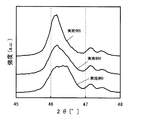
実施例1〜11及び比較例1〜7の圧電素子300について、Bruker AXS社製の「D8 Discover」を用い、X線源にCuKα線を使用し、室温で粉末X線回折パターンを求めた。その結果、実施例1〜11及び比較例1〜7すべてにおいて、ABO3由来の回折ピーク、基板であるSi由来のピーク、Pt(111)由来のピーク、およびPt(111)のCuKβ線の回折に由来するピークが観測された。以上の結果から、実施例1〜11及び比較例1〜7の圧電体層はABO3型構造を形成していることがわかる。結果の一例として、回折強度−回折角2θの相関関係を示す図であるX線回折パターンを、実施例4、11及び比較例2〜3について図18及び図19に、実施例5、6及び9について図20に示す。なお、図19は図18の拡大図である。
(Test Example 2)
For the
そして、図18及び19に示すように、実施例4は2θ=46.1°近傍に回折ピークを持つのに対し、比較例2及び3は2θ=46.5°近傍に回折ピークを持ち、実施例11はその両方の回折ピークが混在している。前述のP−Eヒステリシス形状より、比較例2及び3は反強誘電体であり、実施例4は強誘電体であるので、2θ=46.5°の回折ピークは反強誘電性を示す相に、2θ=46.1°の回折ピークは強誘電性を示す相に由来する回折ピークに帰属される。以上のことから、実施例11は強誘電体に起因する構造と反強誘電体に起因する構造の両者が共存する組成相境界(M.P.B.)であることがわかる。基板とABO3以外のピークは観測されず、異相は存在しないことが分かる。 As shown in FIGS. 18 and 19, Example 4 has a diffraction peak in the vicinity of 2θ = 46.1 °, while Comparative Examples 2 and 3 have a diffraction peak in the vicinity of 2θ = 46.5 °. In Example 11, both diffraction peaks are mixed. From the above-mentioned PE hysteresis shape, Comparative Examples 2 and 3 are antiferroelectric materials, and Example 4 is a ferroelectric material. Therefore, the diffraction peak at 2θ = 46.5 ° is a phase exhibiting antiferroelectric properties. In addition, the diffraction peak at 2θ = 46.1 ° is attributed to a diffraction peak derived from a phase exhibiting ferroelectricity. From the above, it can be seen that Example 11 is a composition phase boundary (MPB) in which both a structure caused by a ferroelectric substance and a structure caused by an antiferroelectric substance coexist. It can be seen that no peaks other than the substrate and ABO 3 are observed, and no heterogeneous phase exists.
また、図20に示すように、2θ=45〜48°において、(Bi1-x,Lax)(Fe1-y,Mny)O3およびSiのピークが観測され、いずれの実施例においても強度比こそ異なるものの、強誘電性を示す相と反強誘電性を示す相の回折ピークが共存した回折パターンが得られた。 Further, as shown in FIG. 20, in the 2θ = 45~48 °, (Bi 1 -x, La x) (Fe 1-y, Mn y) peak of O 3 and Si were observed in any of the embodiments Although the intensity ratios were different, a diffraction pattern in which diffraction peaks of a phase exhibiting ferroelectricity and a phase exhibiting antiferroelectricity coexisted was obtained.
したがって、XRDの結果から、(Bi1-x,Lax)(Fe1-y,Mny)O3で0.17≦x≦0.20のものは、反強誘電相と強誘電相のM.P.B.であることがわかった。
Therefore, from the results of XRD, (Bi 1-x, La x) (Fe 1-y, Mn y)
また、図20に示す回折パターンを、Bruker製X線構造解析ソフトであるTopas2.1にてピークフィッティングを行うことで、強誘電性を示す相由来の回折ピークの面積強度(AF)および反強誘電性を示す相由来の回折ピークの面積強度(AAF)を算出した。ピーク関数はPearsonIVを使用し、装置および結晶性に依存する半値半幅(FWHM)は強誘電体由来のピークと反強誘電体由来のピークで同一の値を使用した。この結果、実施例5ではAAF/AF=0.1、実施例6ではAAF/AF=0.5、実施例9ではAAF/AF=0.9であった。 Further, the diffraction pattern shown in FIG. 20 is subjected to peak fitting with Topas 2.1 which is an X-ray structure analysis software manufactured by Bruker, so that the area intensity (A F ) and anti-phase of a diffraction peak derived from a phase exhibiting ferroelectricity are obtained. The area intensity (A AF ) of the diffraction peak derived from the phase showing ferroelectricity was calculated. Pearson IV was used as the peak function, and the half-width (FWHM) depending on the apparatus and crystallinity was the same for the peak derived from the ferroelectric and the peak derived from the antiferroelectric. As a result, A AF / A F = 0.1 in Example 5, A AF / A F = 0.5 in Example 6, and A AF / A F = 0.9 in Example 9.
(試験例3)
実施例1〜11及び比較例1〜7の各圧電素子300について、アグザクト社製の変位測定装置(DBLI)を用い室温で、φ=500μmの電極パターンを使用し、周波数1kHzの電圧を印加して、電界誘起歪―電界強度の関係を求めた。結果の一例として、実施例4,11及び比較例3について図21〜23に、実施例5、6及び9については図24〜26に示す。
(Test Example 3)
About each
図21〜23に示すように、+30Vにおける変位量は、実施例4においては1.10nm、実施例11においては1.43nm、比較例3においては1.72nmであった。試験例3において、実施例11は図19に示すように反強誘電相と強誘電相のM.P.B.であり、それを反映し歪み量においても1.3倍の電界誘起歪が得られた。これは膜厚で規格化した歪率に換算すると0.36%であり、実用化されているPZTの歪率に匹敵する非常に大きな値である。また、実施例4及び11では、+30Vから−7Vの範囲で強誘電体に特徴的な直線的な電界誘起歪の電圧応答が観測された。 As shown in FIGS. 21 to 23, the displacement amount at +30 V was 1.10 nm in Example 4, 1.43 nm in Example 11, and 1.72 nm in Comparative Example 3. In Test Example 3, Example 11 shows an antiferroelectric phase and a ferroelectric phase of M.I. P. B. Reflecting this, 1.3 times as much electric field induced strain was obtained in the amount of strain. This is 0.36% in terms of the strain rate normalized by the film thickness, which is a very large value comparable to the strain rate of PZT that is in practical use. In Examples 4 and 11, a linear electric field-induced strain voltage response characteristic of the ferroelectric was observed in the range of + 30V to -7V.
そして、比較例3は実施例11と比較し、1.2倍の電界誘起歪が観測された。しかしながら、比較例3は反強誘電体であり、それを反映し0Vから+10Vの範囲でほとんど電界誘起歪を示さず、+10Vから0Vの範囲で電界誘起歪の電圧応答の折れ曲がりが観測された。 In Comparative Example 3, a field-induced strain 1.2 times that in Example 11 was observed. However, Comparative Example 3 is an antiferroelectric material, reflecting almost no electric field induced strain in the range of 0V to + 10V, and bending of the voltage response of the electric field induced strain was observed in the range of + 10V to 0V.
以上の結果から、(Bi1-x,Lax)(Fe1-y,Mny)O3では、反強誘電体がもっとも大きな電界誘起歪を示すが、強誘電体の(Bi1-x,Lax)(Fe1-y,Mny)O3、すなわち、0.10≦x≦0.20,0.01≦y≦0.09の範囲内では、強誘電相に起因する構造と反強誘電相に起因する構造の両者が共存する組成相境界(M.P.B.)に近づく、すなわち、0.17≦x≦0.20、さらには0.19≦x≦0.20となるにつれ、PZTの歪率に匹敵する大きな電界誘起歪を示すとともに、反強誘電体では示さない電圧に対する歪み量が良好な直線性を示すことがわかった。 From the above results, (Bi 1-x, La x) (Fe 1-y, Mn y) in O 3, anti-ferroelectric but most showing a large electric field-induced strain, ferroelectric (Bi 1-x , La x ) (Fe 1-y , Mny y ) O 3 , that is, within the range of 0.10 ≦ x ≦ 0.20 and 0.01 ≦ y ≦ 0.09, It approaches the composition phase boundary (MPB) where both of the structures caused by the antiferroelectric phase coexist, that is, 0.17 ≦ x ≦ 0.20, and further 0.19 ≦ x ≦ 0.20. As a result, it was found that a large electric field induced strain comparable to the strain rate of PZT was exhibited, and that the amount of strain with respect to a voltage not exhibited by the antiferroelectric material showed good linearity.
また、図26に示すように、実施例9において30Vにおける変位量が1.44nmと最も良好な値を示した。それに加え、図24及び25に示すように、実施例5及び6においても実施例9に対し変位低下が10%未満に抑えられている。このことから、反強誘電体の組成に近づけることで変位量は増加するが、少なくともAAF/AF=0.1であるx=0.78の組成においても、AAF/AF=0.9であるx=0.20の90%以上の変位量を示した。このことから、少なくともXRDにてAAF/AF>0.1程度の強度比が観測される組成であれば、AAF/AF=0.9の組成と遜色ない圧電性を示すことがわかった。 Further, as shown in FIG. 26, the displacement amount at 30 V in Example 9 was 1.44 nm, which was the best value. In addition, as shown in FIGS. 24 and 25, in Examples 5 and 6, the decrease in displacement is suppressed to less than 10% compared to Example 9. From this, the amount of displacement increases by approaching the composition of the antiferroelectric material, but at least A AF / A F = 0 even in the composition of x = 0.78 where A AF / A F = 0.1. A displacement amount of 90% or more with x = 0.20, which is .9. From this, at least the composition with an intensity ratio of about A AF / A F > 0.1 observed by XRD can exhibit piezoelectricity comparable to the composition of A AF / A F = 0.9. all right.
このような圧電素子300の個別電極である各第2電極80には、インク供給路14側の端部近傍から引き出され、絶縁体膜55上にまで延設される、例えば、金(Au)等からなるリード電極90が接続されている。
Each
このような圧電素子300が形成された流路形成基板10上、すなわち、第1電極60、絶縁体膜55及びリード電極90上には、リザーバー100の少なくとも一部を構成するリザーバー部31を有する保護基板30が接着剤35を介して接合されている。このリザーバー部31は、本実施形態では、保護基板30を厚さ方向に貫通して圧力発生室12の幅方向に亘って形成されており、上述のように流路形成基板10の連通部13と連通されて各圧力発生室12の共通のインク室となるリザーバー100を構成している。また、流路形成基板10の連通部13を圧力発生室12毎に複数に分割して、リザーバー部31のみをリザーバーとしてもよい。さらに、例えば、流路形成基板10に圧力発生室12のみを設け、流路形成基板10と保護基板30との間に介在する部材(例えば、弾性膜50、絶縁体膜55等)にリザーバーと各圧力発生室12とを連通するインク供給路14を設けるようにしてもよい。
On the flow
また、保護基板30の圧電素子300に対向する領域には、圧電素子300の運動を阻害しない程度の空間を有する圧電素子保持部32が設けられている。圧電素子保持部32は、圧電素子300の運動を阻害しない程度の空間を有していればよく、当該空間は密封されていても、密封されていなくてもよい。
A piezoelectric
このような保護基板30としては、流路形成基板10の熱膨張率と略同一の材料、例えば、ガラス、セラミック材料等を用いることが好ましく、本実施形態では、流路形成基板10と同一材料のシリコン単結晶基板を用いて形成した。
As such a
また、保護基板30には、保護基板30を厚さ方向に貫通する貫通孔33が設けられている。そして、各圧電素子300から引き出されたリード電極90の端部近傍は、貫通孔33内に露出するように設けられている。
The
また、保護基板30上には、並設された圧電素子300を駆動するための駆動回路120が固定されている。この駆動回路120としては、例えば、回路基板や半導体集積回路(IC)等を用いることができる。そして、駆動回路120とリード電極90とは、ボンディングワイヤー等の導電性ワイヤーからなる接続配線121を介して電気的に接続されている。
A
また、このような保護基板30上には、封止膜41及び固定板42とからなるコンプライアンス基板40が接合されている。ここで、封止膜41は、剛性が低く可撓性を有する材料からなり、この封止膜41によってリザーバー部31の一方面が封止されている。また、固定板42は、比較的硬質の材料で形成されている。この固定板42のリザーバー100に対向する領域は、厚さ方向に完全に除去された開口部43となっているため、リザーバー100の一方面は可撓性を有する封止膜41のみで封止されている。
In addition, a
このような本実施形態のインクジェット式記録ヘッドIでは、図示しない外部のインク供給手段と接続したインク導入口からインクを取り込み、リザーバー100からノズル開口21に至るまで内部をインクで満たした後、駆動回路120からの記録信号に従い、圧力発生室12に対応するそれぞれの第1電極60と第2電極80との間に電圧を印加し、弾性膜50、絶縁体膜55、第1電極60及び圧電体層70をたわみ変形させることにより、各圧力発生室12内の圧力が高まりノズル開口21からインク滴が吐出する。
In such an ink jet recording head I of this embodiment, ink is taken in from an ink introduction port connected to an external ink supply means (not shown), and the interior from the
(他の実施形態)
以上、本発明の一実施形態を説明したが、本発明の基本的構成は上述したものに限定されるものではない。例えば、上述した実施形態では、金属元素として、Bi、La、Fe及びMnのみを含有するABO3型の複合酸化物について記載したが、Bi、La、Fe及びMnを含むABO3型の複合酸化物であればよく、圧電特性を良好にする等のために、他の金属を添加してもよい。
(Other embodiments)
As mentioned above, although one Embodiment of this invention was described, the basic composition of this invention is not limited to what was mentioned above. For example, in the embodiment described above, as the metal element, Bi, La, has been described ABO 3 type composite oxide containing only Fe and Mn, Bi, La, the ABO 3 type containing Fe and Mn complex oxide Any other metal may be added to improve the piezoelectric characteristics.
また、上述した実施形態では、流路形成基板10として、シリコン単結晶基板を例示したが、特にこれに限定されず、例えば、SOI基板、ガラス等の材料を用いるようにしてもよい。
In the embodiment described above, a silicon single crystal substrate is exemplified as the flow
さらに、上述した実施形態では、基板(流路形成基板10)上に第1電極60、圧電体層70及び第2電極80を順次積層した圧電素子300を例示したが、特にこれに限定されず、例えば、圧電材料と電極形成材料とを交互に積層させて軸方向に伸縮させる縦振動型の圧電素子にも本発明を適用することができる。
Furthermore, in the above-described embodiment, the
また、これら実施形態のインクジェット式記録ヘッドは、インクカートリッジ等と連通するインク流路を具備する記録ヘッドユニットの一部を構成して、インクジェット式記録装置に搭載される。図27は、そのインクジェット式記録装置の一例を示す概略図である。 In addition, the ink jet recording head of these embodiments constitutes a part of a recording head unit including an ink flow path communicating with an ink cartridge or the like, and is mounted on the ink jet recording apparatus. FIG. 27 is a schematic view showing an example of the ink jet recording apparatus.
図27に示すインクジェット式記録装置IIにおいて、インクジェット式記録ヘッドIを有する記録ヘッドユニット1A及び1Bは、インク供給手段を構成するカートリッジ2A及び2Bが着脱可能に設けられ、この記録ヘッドユニット1A及び1Bを搭載したキャリッジ3は、装置本体4に取り付けられたキャリッジ軸5に軸方向移動自在に設けられている。この記録ヘッドユニット1A及び1Bは、例えば、それぞれブラックインク組成物及びカラーインク組成物を吐出するものとしている。
In the ink jet recording apparatus II shown in FIG. 27, the
そして、駆動モーター6の駆動力が図示しない複数の歯車およびタイミングベルト7を介してキャリッジ3に伝達されることで、記録ヘッドユニット1A及び1Bを搭載したキャリッジ3はキャリッジ軸5に沿って移動される。一方、装置本体4にはキャリッジ軸5に沿ってプラテン8が設けられており、図示しない給紙ローラーなどにより給紙された紙等の記録媒体である記録シートSがプラテン8に巻き掛けられて搬送されるようになっている。
The driving force of the driving
なお、上述した実施形態1では、液体噴射ヘッドの一例としてインクジェット式記録ヘッドを挙げて説明したが、本発明は広く液体噴射ヘッド全般を対象としたものであり、インク以外の液体を噴射する液体噴射ヘッドにも勿論適用することができる。その他の液体噴射ヘッドとしては、例えば、プリンター等の画像記録装置に用いられる各種の記録ヘッド、液晶ディスプレイ等のカラーフィルターの製造に用いられる色材噴射ヘッド、有機ELディスプレイ、FED(電界放出ディスプレイ)等の電極形成に用いられる電極材料噴射ヘッド、バイオchip製造に用いられる生体有機物噴射ヘッド等が挙げられる。 In the first embodiment described above, an ink jet recording head has been described as an example of a liquid ejecting head. However, the present invention is widely intended for all liquid ejecting heads, and is a liquid ejecting a liquid other than ink. Of course, the present invention can also be applied to an ejection head. Other liquid ejecting heads include, for example, various recording heads used in image recording apparatuses such as printers, color material ejecting heads used in the manufacture of color filters such as liquid crystal displays, organic EL displays, and FEDs (field emission displays). Examples thereof include an electrode material ejection head used for electrode formation, a bioorganic matter ejection head used for biochip production, and the like.
また、本発明は、インクジェット式記録ヘッドに代表される液体噴射ヘッドに搭載される圧電素子に限られず、超音波発信機等の超音波デバイス、超音波モーター、圧力センサー、強誘電体メモリー等の圧電素子にも同様に適用することができる。 Further, the present invention is not limited to a piezoelectric element mounted on a liquid jet head typified by an ink jet recording head, but includes an ultrasonic device such as an ultrasonic transmitter, an ultrasonic motor, a pressure sensor, a ferroelectric memory, and the like. The present invention can be similarly applied to a piezoelectric element.
I インクジェット式記録ヘッド(液体噴射ヘッド)、 II インクジェット式記録装置(液体噴射装置)、 10 流路形成基板、 12 圧力発生室、 13 連通部、 14 インク供給路、 20 ノズルプレート、 21 ノズル開口、 30 保護基板、 31 リザーバー部、 32 圧電素子保持部、 40 コンプライアンス基板、 60 第1電極、 70 圧電体層、 80 第2電極、 90 リード電極、 100 リザーバー、 120 駆動回路、 121 接続配線、 300 圧電素子 I ink jet recording head (liquid ejecting head), II ink jet recording apparatus (liquid ejecting apparatus), 10 flow path forming substrate, 12 pressure generating chamber, 13 communicating portion, 14 ink supply path, 20 nozzle plate, 21 nozzle opening, 30 protection substrate, 31 reservoir section, 32 piezoelectric element holding section, 40 compliance substrate, 60 first electrode, 70 piezoelectric layer, 80 second electrode, 90 lead electrode, 100 reservoir, 120 drive circuit, 121 connection wiring, 300 piezoelectric element
Claims (6)
粉末X線回折パターンにおいて、強誘電性を示す相に帰属される回折ピークと、反強誘電性を示す相に帰属される回折ピークが同時に観測されることを特徴とする圧電材料。
(Bi 1-x ,La x )(Fe 1-y ,Mn y )O 3
(0.17≦x≦0.20,0.01≦y≦0.09) It consists of a perovskite complex oxide represented by the following general formula:
A piezoelectric material, wherein a diffraction peak attributed to a phase exhibiting ferroelectricity and a diffraction peak attributed to a phase exhibiting antiferroelectricity are simultaneously observed in a powder X-ray diffraction pattern.
(Bi 1-x, La x ) (Fe 1-y, Mn y) O 3
(0.17 ≦ x ≦ 0.20, 0.01 ≦ y ≦ 0.09)
Priority Applications (5)
| Application Number | Priority Date | Filing Date | Title |
|---|---|---|---|
| JP2010115744A JP5621964B2 (en) | 2009-11-02 | 2010-05-19 | Liquid ejecting head, liquid ejecting apparatus, piezoelectric element, and ultrasonic device |
| EP20100185460 EP2317579B1 (en) | 2009-11-02 | 2010-10-01 | Liquid-ejecting head, liquid-ejecting apparatus, piezoelectric element, and piezoelectric material |
| US12/914,233 US8678560B2 (en) | 2009-11-02 | 2010-10-28 | Liquid-ejecting head, liquid-ejecting apparatus, piezoelectric element, and piezoelectric material |
| CN2010105309846A CN102139565B (en) | 2009-11-02 | 2010-11-02 | Liquid-ejecting head, liquid-ejecting apparatus, piezoelectric element, and piezoelectric material |
| US14/102,377 US9799820B2 (en) | 2009-11-02 | 2013-12-10 | Liquid-ejecting head, liquid-ejecting apparatus, piezoelectric element, and piezoelectric material |
Applications Claiming Priority (5)
| Application Number | Priority Date | Filing Date | Title |
|---|---|---|---|
| JP2009252445 | 2009-11-02 | ||
| JP2009252445 | 2009-11-02 | ||
| JP2010052430 | 2010-03-09 | ||
| JP2010052430 | 2010-03-09 | ||
| JP2010115744A JP5621964B2 (en) | 2009-11-02 | 2010-05-19 | Liquid ejecting head, liquid ejecting apparatus, piezoelectric element, and ultrasonic device |
Publications (3)
| Publication Number | Publication Date |
|---|---|
| JP2011211141A JP2011211141A (en) | 2011-10-20 |
| JP2011211141A5 JP2011211141A5 (en) | 2013-10-17 |
| JP5621964B2 true JP5621964B2 (en) | 2014-11-12 |
Family
ID=43530428
Family Applications (1)
| Application Number | Title | Priority Date | Filing Date |
|---|---|---|---|
| JP2010115744A Expired - Fee Related JP5621964B2 (en) | 2009-11-02 | 2010-05-19 | Liquid ejecting head, liquid ejecting apparatus, piezoelectric element, and ultrasonic device |
Country Status (4)
| Country | Link |
|---|---|
| US (2) | US8678560B2 (en) |
| EP (1) | EP2317579B1 (en) |
| JP (1) | JP5621964B2 (en) |
| CN (1) | CN102139565B (en) |
Families Citing this family (12)
| Publication number | Priority date | Publication date | Assignee | Title |
|---|---|---|---|---|
| JP5660274B2 (en) * | 2010-01-05 | 2015-01-28 | セイコーエプソン株式会社 | Liquid ejecting head manufacturing method, piezoelectric element manufacturing method, liquid ejecting head, liquid ejecting apparatus, and piezoelectric element |
| JP5660288B2 (en) * | 2010-01-05 | 2015-01-28 | セイコーエプソン株式会社 | Liquid ejecting head, liquid ejecting apparatus, piezoelectric element, and liquid ejecting head manufacturing method |
| JP5641185B2 (en) * | 2010-01-05 | 2014-12-17 | セイコーエプソン株式会社 | Liquid ejecting head, liquid ejecting apparatus, and piezoelectric element |
| JP5556182B2 (en) * | 2010-01-05 | 2014-07-23 | セイコーエプソン株式会社 | Liquid ejecting head, liquid ejecting apparatus, and piezoelectric element |
| JP5672433B2 (en) | 2010-03-12 | 2015-02-18 | セイコーエプソン株式会社 | Liquid ejecting head, liquid ejecting apparatus, piezoelectric element, pyroelectric element, and IR sensor |
| JP2011211143A (en) * | 2010-03-12 | 2011-10-20 | Seiko Epson Corp | Liquid discharge head, liquid discharge device, and piezoelectric element |
| JP2014185982A (en) | 2013-03-25 | 2014-10-02 | Seiko Epson Corp | Infrared sensor and thermal detector element |
| JP6264525B2 (en) | 2013-03-25 | 2018-01-24 | セイコーエプソン株式会社 | Infrared sensor, heat detection element, and heat detection method using the same |
| US9503656B2 (en) | 2013-12-11 | 2016-11-22 | Seiko Epson Corporation | Solid state imaging device and image acquisition method using solid state imaging elements having a PN junction |
| JP2015198155A (en) | 2014-04-01 | 2015-11-09 | セイコーエプソン株式会社 | Thermoelectric conversion element, photo-detection device and electronic device |
| US11121139B2 (en) * | 2017-11-16 | 2021-09-14 | International Business Machines Corporation | Hafnium oxide and zirconium oxide based ferroelectric devices with textured iridium bottom electrodes |
| JP2022152144A (en) * | 2021-03-29 | 2022-10-12 | セイコーエプソン株式会社 | Liquid jet head and liquid jet device |
Family Cites Families (28)
| Publication number | Priority date | Publication date | Assignee | Title |
|---|---|---|---|---|
| JPH04266036A (en) | 1991-02-21 | 1992-09-22 | Toppan Printing Co Ltd | Semiconductor device in plastic package |
| JPH0817245A (en) | 1994-06-30 | 1996-01-19 | Tdk Corp | Ferro-electric thin film and manufacture thereof |
| JPH1052071A (en) | 1996-07-31 | 1998-02-20 | Ricoh Co Ltd | Antiferroelectric-ferroelectric phase transition film actuator and ink-jet printer |
| JP2000127392A (en) | 1998-10-29 | 2000-05-09 | Ricoh Co Ltd | Lead based dielectric ceramic and actuator employing it |
| JP4051654B2 (en) | 2000-02-08 | 2008-02-27 | セイコーエプソン株式会社 | Piezoelectric element, ink jet recording head, manufacturing method thereof, and ink jet printer |
| JP2001335362A (en) | 2000-05-26 | 2001-12-04 | Tdk Corp | Piezoelectric ceramic and piezoelectric device using it |
| JP2003267796A (en) * | 2002-03-15 | 2003-09-25 | Akio Ikesue | Oxide having perovskite structure and method for producing the same |
| JP4842520B2 (en) * | 2003-05-30 | 2011-12-21 | 日本碍子株式会社 | Cell driving type piezoelectric / electrostrictive actuator and manufacturing method thereof |
| JP4165347B2 (en) | 2003-06-25 | 2008-10-15 | セイコーエプソン株式会社 | Method for manufacturing piezoelectric element |
| JP2006176366A (en) | 2004-12-22 | 2006-07-06 | Fujitsu Ltd | Ferroelectric material, method for manufacturing the same, and ferroelectric memory |
| JP5121186B2 (en) * | 2005-08-23 | 2013-01-16 | キヤノン株式会社 | Piezoelectric body, piezoelectric element, liquid discharge head, and liquid discharge apparatus |
| JP4237208B2 (en) | 2005-09-26 | 2009-03-11 | 富士フイルム株式会社 | Piezoelectric element and driving method thereof, piezoelectric device, and liquid ejection device |
| JP2007194429A (en) | 2006-01-19 | 2007-08-02 | Fujitsu Ltd | Ferromagnetic and ferroelectric materials and semiconductor devices |
| JP5035504B2 (en) | 2006-04-12 | 2012-09-26 | セイコーエプソン株式会社 | Inkjet recording head and inkjet printer |
| JP2008192868A (en) | 2007-02-06 | 2008-08-21 | Fujifilm Corp | Piezoelectric film and piezoelectric element using the same, and liquid discharge device |
| US20080239016A1 (en) | 2007-03-26 | 2008-10-02 | Canon Kabushiki Kaisha | Liquid discharge head and liquid discharge apparatus |
| JP4266036B2 (en) | 2007-04-26 | 2009-05-20 | 富士フイルム株式会社 | Piezoelectric body, piezoelectric element, and liquid ejection device |
| US7786656B2 (en) | 2007-04-26 | 2010-08-31 | Fujifilm Corporation | Piezoelectric body, piezoelectric device, and liquid discharge apparatus |
| JP5307986B2 (en) | 2007-05-07 | 2013-10-02 | 富士フイルム株式会社 | Piezoelectric element, manufacturing method thereof, and liquid ejection device |
| JP2008311634A (en) | 2007-05-14 | 2008-12-25 | Fujifilm Corp | Piezoelectric element, method for driving the same, piezoelectric device, and liquid discharge device |
| JP5095315B2 (en) * | 2007-09-05 | 2012-12-12 | 富士フイルム株式会社 | Perovskite oxide, ferroelectric film and manufacturing method thereof, ferroelectric element, and liquid ejection device |
| JP4276276B2 (en) * | 2007-09-07 | 2009-06-10 | 富士フイルム株式会社 | Method for manufacturing piezoelectric element |
| JP5507097B2 (en) | 2008-03-12 | 2014-05-28 | 富士フイルム株式会社 | Perovskite oxide and method for producing the same, piezoelectric body, piezoelectric element, and liquid ejection device |
| JP5267971B2 (en) | 2008-03-21 | 2013-08-21 | 国立大学法人金沢大学 | Ferroelectric material and piezoelectric material |
| JP2009245893A (en) * | 2008-03-31 | 2009-10-22 | Toshiba Corp | Light-emitting device sealing structure and method for manufacturing the same |
| JP5248168B2 (en) | 2008-04-01 | 2013-07-31 | セイコーエプソン株式会社 | Piezoelectric material and piezoelectric element |
| JP5110703B2 (en) | 2008-05-28 | 2012-12-26 | 富士フイルム株式会社 | Perovskite oxide film, ferroelectric, piezoelectric element, liquid ejection device |
| JP5534179B2 (en) * | 2010-03-09 | 2014-06-25 | セイコーエプソン株式会社 | Piezoelectric film, piezoelectric element, liquid ejecting head, and liquid ejecting apparatus |
-
2010
- 2010-05-19 JP JP2010115744A patent/JP5621964B2/en not_active Expired - Fee Related
- 2010-10-01 EP EP20100185460 patent/EP2317579B1/en not_active Not-in-force
- 2010-10-28 US US12/914,233 patent/US8678560B2/en active Active
- 2010-11-02 CN CN2010105309846A patent/CN102139565B/en not_active Expired - Fee Related
-
2013
- 2013-12-10 US US14/102,377 patent/US9799820B2/en not_active Expired - Fee Related
Also Published As
| Publication number | Publication date |
|---|---|
| EP2317579A3 (en) | 2013-10-02 |
| EP2317579B1 (en) | 2015-03-25 |
| CN102139565B (en) | 2013-11-06 |
| US9799820B2 (en) | 2017-10-24 |
| US20140097724A1 (en) | 2014-04-10 |
| CN102139565A (en) | 2011-08-03 |
| EP2317579A2 (en) | 2011-05-04 |
| JP2011211141A (en) | 2011-10-20 |
| US20110102517A1 (en) | 2011-05-05 |
| US8678560B2 (en) | 2014-03-25 |
Similar Documents
| Publication | Publication Date | Title |
|---|---|---|
| JP5621964B2 (en) | Liquid ejecting head, liquid ejecting apparatus, piezoelectric element, and ultrasonic device | |
| JP5839157B2 (en) | Liquid ejecting head, liquid ejecting apparatus, piezoelectric element, ultrasonic sensor and infrared sensor | |
| JP5854183B2 (en) | Liquid ejecting head, liquid ejecting apparatus, piezoelectric element, ultrasonic sensor and infrared sensor | |
| JP5825466B2 (en) | Liquid ejecting head, liquid ejecting apparatus, and piezoelectric element | |
| JP5672433B2 (en) | Liquid ejecting head, liquid ejecting apparatus, piezoelectric element, pyroelectric element, and IR sensor | |
| JP5716897B2 (en) | Liquid ejecting head, liquid ejecting apparatus, piezoelectric element, ultrasonic sensor and infrared sensor | |
| JP5854184B2 (en) | Liquid ejecting head, liquid ejecting apparatus, piezoelectric element, ultrasonic sensor and infrared sensor | |
| CN102205721B (en) | Liquid ejecting head, liquid ejecting apparatus, and piezoelectric element | |
| JP5668473B2 (en) | Piezoelectric element and method for manufacturing the same, liquid ejecting head, liquid ejecting apparatus, ultrasonic sensor, and infrared sensor | |
| JP5733487B2 (en) | Liquid ejecting head, liquid ejecting apparatus, ultrasonic device, piezoelectric element, and piezoelectric material | |
| JP5773129B2 (en) | Liquid ejecting head, liquid ejecting apparatus, piezoelectric element, ultrasonic device, and IR sensor | |
| JP5585197B2 (en) | Liquid ejecting head, liquid ejecting apparatus, and piezoelectric element | |
| JP5884959B2 (en) | Piezoelectric film manufacturing method, piezoelectric element, liquid jet head, and liquid jet apparatus | |
| JP6146599B2 (en) | Piezoelectric element, liquid ejecting head, liquid ejecting apparatus, ultrasonic device and sensor | |
| JP5754619B2 (en) | Liquid ejecting head, liquid ejecting apparatus, piezoelectric element, ultrasonic sensor and infrared sensor | |
| US8657417B2 (en) | Piezoelectric element, liquid ejecting head, and liquid ejecting apparatus | |
| JP5765525B2 (en) | Liquid ejecting head, liquid ejecting apparatus, piezoelectric element, ultrasonic device, and IR sensor | |
| JP5991457B2 (en) | Liquid ejecting head, liquid ejecting apparatus, piezoelectric element, and piezoelectric material | |
| JP2013165195A (en) | Liquid injection head, liquid injection device and piezoelectric element | |
| JP2013052641A (en) | Liquid ejecting head, liquid ejection device, and piezoelectric element | |
| JP2013115386A (en) | Liquid injection head and liquid injector and piezoelectric element | |
| JP2013080801A (en) | Liquid jet head, liquid jet apparatus and piezoelectric element | |
| JP2012164893A (en) | Liquid-ejecting head and liquid-ejecting apparatus, and piezoelectric device |
Legal Events
| Date | Code | Title | Description |
|---|---|---|---|
| A621 | Written request for application examination |
Free format text: JAPANESE INTERMEDIATE CODE: A621 Effective date: 20130329 |
|
| A521 | Request for written amendment filed |
Free format text: JAPANESE INTERMEDIATE CODE: A523 Effective date: 20130902 |
|
| A131 | Notification of reasons for refusal |
Free format text: JAPANESE INTERMEDIATE CODE: A131 Effective date: 20140625 |
|
| A521 | Request for written amendment filed |
Free format text: JAPANESE INTERMEDIATE CODE: A523 Effective date: 20140808 |
|
| TRDD | Decision of grant or rejection written | ||
| A01 | Written decision to grant a patent or to grant a registration (utility model) |
Free format text: JAPANESE INTERMEDIATE CODE: A01 Effective date: 20140827 |
|
| A61 | First payment of annual fees (during grant procedure) |
Free format text: JAPANESE INTERMEDIATE CODE: A61 Effective date: 20140909 |
|
| R150 | Certificate of patent or registration of utility model |
Ref document number: 5621964 Country of ref document: JP Free format text: JAPANESE INTERMEDIATE CODE: R150 |
|
| S531 | Written request for registration of change of domicile |
Free format text: JAPANESE INTERMEDIATE CODE: R313531 |
|
| R350 | Written notification of registration of transfer |
Free format text: JAPANESE INTERMEDIATE CODE: R350 |
|
| LAPS | Cancellation because of no payment of annual fees |