JP5590981B2 - Semiconductor device - Google Patents
Semiconductor device Download PDFInfo
- Publication number
- JP5590981B2 JP5590981B2 JP2010135261A JP2010135261A JP5590981B2 JP 5590981 B2 JP5590981 B2 JP 5590981B2 JP 2010135261 A JP2010135261 A JP 2010135261A JP 2010135261 A JP2010135261 A JP 2010135261A JP 5590981 B2 JP5590981 B2 JP 5590981B2
- Authority
- JP
- Japan
- Prior art keywords
- semiconductor device
- molten solder
- main body
- electrode terminal
- electrode
- Prior art date
- Legal status (The legal status is an assumption and is not a legal conclusion. Google has not performed a legal analysis and makes no representation as to the accuracy of the status listed.)
- Expired - Fee Related
Links
Images


Landscapes
- Electric Connection Of Electric Components To Printed Circuits (AREA)
- Lead Frames For Integrated Circuits (AREA)
Description
本発明は、半導体装置、半導体装置の実装方法、および実装用治具に関し、より特定的には、プリント配線板の表面に実装される半導体装置、プリント配線板の表面に半導体装置を実装するために使用される半導体装置の実装方法、および、この半導体装置の実装方法に用いられる実装用治具に関する。 The present invention relates to a semiconductor device, a semiconductor device mounting method, and a mounting jig, and more specifically, a semiconductor device mounted on the surface of a printed wiring board, and a semiconductor device mounted on the surface of the printed wiring board. The present invention relates to a mounting method of a semiconductor device used for the above-mentioned and a mounting jig used for the mounting method of the semiconductor device.
SOP(Small Outline Package)、またはQFP(Quad Flat Package)等の半導体装置は、電子部品としてプリント配線板の表面に実装される。プリント配線板にこれらの電子部品を実装するために、リフローはんだ付け法(以下、リフロー法とも称する)、またはフローはんだ付け法等が使用されている。 A semiconductor device such as SOP (Small Outline Package) or QFP (Quad Flat Package) is mounted on the surface of a printed wiring board as an electronic component. In order to mount these electronic components on a printed wiring board, a reflow soldering method (hereinafter also referred to as a reflow method), a flow soldering method, or the like is used.
リフロー法では、電子部品の電極端子とプリント配線板の配線電極との間にソルダペーストが予め供給される。ソルダペーストは、はんだ粉とフラックスとを含んで構成されている。ソルダペーストを含む系全体が加熱されることによって、ソルダペーストが溶融する。その後系全体が冷却されることによって、ソルダペーストが凝固する。この凝固によって、電子部品の電極端子とプリント配線板の配線電極とが接合される。 In the reflow method, a solder paste is supplied in advance between the electrode terminal of the electronic component and the wiring electrode of the printed wiring board. The solder paste is configured to include solder powder and flux. The solder paste is melted by heating the entire system including the solder paste. Thereafter, the solder paste is solidified by cooling the entire system. By this solidification, the electrode terminal of the electronic component and the wiring electrode of the printed wiring board are joined.
フローはんだ付け法には、溶融はんだ液面を動かさない静止槽方式(DIP方式)、および、溶融はんだ液面に波を立てる噴流方式(フロー方式)の2つの方式がある。フローはんだ付け法(上記の2つの方式を含む)では、プリント配線板における電子部品が仮固定された面を下方に向けた状態で、プリント配線板が溶融はんだに浸漬される。溶融はんだは、電子部品の電極端子およびプリント配線板の配線電極に接触する。この接触によって金属結合(「濡れ」と呼ばれる)が起こる。この濡れによって、溶融状態にあるはんだが、電子部品の電極端子とプリント配線板の配線電極との間に挟まれる。 There are two types of flow soldering methods: a static bath method (DIP method) that does not move the molten solder liquid surface, and a jet method (flow method) that creates waves on the molten solder liquid surface. In the flow soldering method (including the above two methods), the printed wiring board is immersed in molten solder with the surface of the printed wiring board on which the electronic components are temporarily fixed facing downward. The molten solder contacts the electrode terminals of the electronic component and the wiring electrodes of the printed wiring board. This contact causes a metal bond (called “wetting”). Due to this wetting, molten solder is sandwiched between the electrode terminals of the electronic component and the wiring electrodes of the printed wiring board.
溶融はんだから、プリント配線板および電子部品が引き抜かれる。プリント配線板の配線電極と電子部品の電極端子との間に余剰に供給された溶融はんだは、溶融はんだの自重または溶融はんだの表面張力によってはんだ槽に引き戻される。プリント配線板の配線電極と電子部品の電極端子との接合状態を維持するために必要な所定の量の溶融はんだは、上述の金属結合の作用によってプリント配線板の配線電極と電子部品の電極端子との間に残留する。溶融はんだの温度が低下することによって残留した溶融はんだは凝固する。この凝固によってプリント配線板の配線電極と電子部品の電極端子とが接合される。 A printed wiring board and electronic components are pulled out from the molten solder. The excessively supplied molten solder between the wiring electrode of the printed wiring board and the electrode terminal of the electronic component is pulled back to the solder bath by the weight of the molten solder or the surface tension of the molten solder. The predetermined amount of molten solder necessary to maintain the bonding state between the wiring electrode of the printed wiring board and the electrode terminal of the electronic component is caused by the above-described metal bonding to cause the wiring electrode of the printed wiring board and the electrode terminal of the electronic component. It remains between. The remaining molten solder solidifies as the temperature of the molten solder decreases. By this solidification, the wiring electrode of the printed wiring board and the electrode terminal of the electronic component are joined.
上述の2つの方式を含むフローはんだ付け法では、プリント配線板に搭載された電子部品の全体が溶融はんだに浸漬される。電子部品における全ての電極端子は、これらの電極端子が溶融はんだに浸漬された状態では相互に短絡している。溶融はんだからプリント配線板が引き抜かれた後、隣り合う電極端子間を短絡している余剰に供給された溶融はんだが自重または表面張力により取り除かれることによって、短絡のない良好なはんだ接合を得ることができる。 In the flow soldering method including the two methods described above, the entire electronic component mounted on the printed wiring board is immersed in molten solder. All electrode terminals in the electronic component are short-circuited with each other when these electrode terminals are immersed in molten solder. After the printed wiring board is pulled out from the molten solder, the excessively supplied molten solder that short-circuits between the adjacent electrode terminals is removed by its own weight or surface tension, thereby obtaining a good solder joint without a short circuit Can do.
ところが、隣り合う電極端子の間隔が狭い場合、特に電子部品が微細な半導体パッケージであって隣り合う電極端子の間隔がたとえば0.3mmより小さい場合、隣り合う電極端子の間にはんだブリッジが発生することによって隣り合う電極端子が短絡するという問題が生じる。 However, when the interval between the adjacent electrode terminals is narrow, particularly when the electronic component is a fine semiconductor package and the interval between the adjacent electrode terminals is smaller than 0.3 mm, for example, a solder bridge occurs between the adjacent electrode terminals. This causes a problem that adjacent electrode terminals are short-circuited.
このような問題点を解決する手法として、たとえば特開平1−248653号公報(特許文献1)では、電子部品の隣り合う電極端子間に絶縁性の障壁を設けるという手法が提案されている。同文献は、隣り合う電極端子間に溶融はんだが供給され難くなることによって、隣り合う電極端子が短絡することが抑制されると述べている。 As a technique for solving such problems, for example, Japanese Patent Laid-Open No. 1-248653 (Patent Document 1) proposes a technique of providing an insulating barrier between adjacent electrode terminals of an electronic component. The document states that shorting of adjacent electrode terminals is suppressed by making it difficult for molten solder to be supplied between adjacent electrode terminals.
特許文献1においてリフロー法を採用した場合、電子部品の隣り合う電極端子間に設置された絶縁性の障壁によって、溶融はんだの流動による隣り合う電極端子間における短絡の発生は抑制されることが推察される。 When the reflow method is adopted in Patent Document 1, it is inferred that the occurrence of a short circuit between adjacent electrode terminals due to the flow of molten solder is suppressed by an insulating barrier installed between adjacent electrode terminals of an electronic component. Is done.
ここで、特許文献1においてフローはんだ付け法を採用した場合、溶融はんだは電子部品の電極端子間に設けられた絶縁性の障壁を乗り越えることが推察される。隣り合う電極端子間を溶融はんだがアーチ形状(膜状)に繋がることによって、ブリッジが発生してしまう。特許文献1に提案されている手法であっても、フローはんだ付け法を採用した場合においては、隣り合う電極端子同士が短絡するという問題が生じる。 Here, when the flow soldering method is adopted in Patent Document 1, it is presumed that the molten solder overcomes the insulating barrier provided between the electrode terminals of the electronic component. When the molten solder is connected in an arch shape (film shape) between adjacent electrode terminals, a bridge is generated. Even if it is the method proposed by patent document 1, when the flow soldering method is employ | adopted, the problem that adjacent electrode terminals short-circuit arises.
本発明は上述に鑑みてなされたものであり、その目的は、フローはんだ付け法によっても隣り合う電極端子間における短絡の発生を抑制することができる表面実装型の半導体装置、フローはんだ付け法によっても隣り合う電極端子間における短絡の発生を抑制することができる表面実装型の半導体装置の実装方法、および、この半導体装置の実装方法に用いられる実装用治具を提供することにある。 The present invention has been made in view of the above, and an object of the present invention is to provide a surface mounting type semiconductor device capable of suppressing the occurrence of a short circuit between adjacent electrode terminals by a flow soldering method, and a flow soldering method. Another object of the present invention is to provide a mounting method of a surface mounting type semiconductor device capable of suppressing the occurrence of a short circuit between adjacent electrode terminals, and a mounting jig used in the mounting method of the semiconductor device.
本発明の第1の局面に基づく半導体装置は、プリント配線板の表面に実装される半導体装置である。当該半導体装置は、本体と複数の電極端子とを備える。上記本体は、半導体素子を内部に封止する。複数の上記電極端子は、上記本体の側面から突出する突出部、上記突出部の先端から上記本体の下面側に向かって延びる延在部、および、上記延在部の先端から上記本体とは反対側に向かって延びる水平部を有する。 A semiconductor device according to the first aspect of the present invention is a semiconductor device mounted on the surface of a printed wiring board. The semiconductor device includes a main body and a plurality of electrode terminals. The main body seals the semiconductor element inside. The plurality of electrode terminals include a protruding portion protruding from a side surface of the main body, an extending portion extending from the front end of the protruding portion toward the lower surface side of the main body, and the opposite end of the main body from the front end of the extending portion. It has a horizontal part extending toward the side.
上記突出部の上面は、上記側面の高さ方向の中央部より上記下面側に位置している。上記水平部の下面と上記側面の上端との間の高さ方向の寸法は、上記水平部の先端と上記上端との間の幅方向の寸法以上である。 The upper surface of the protruding portion is located on the lower surface side from the central portion of the side surface in the height direction. The dimension in the height direction between the lower surface of the horizontal part and the upper end of the side surface is not less than the dimension in the width direction between the tip of the horizontal part and the upper end.
本発明の第2の局面に基づく半導体装置は、プリント配線板の表面に実装される半導体装置である。当該半導体装置は、本体と張出部と複数の電極端子とを備える。上記本体は、半導体素子を内部に封止する。複数の上記電極端子は、上記本体の側面から突出する突出部、上記突出部の先端から上記本体の下面側に向かって延びる延在部、および、上記延在部の先端から上記本体とは反対側に向かって延びる水平部を有する。上記張出部は、上記電極端子の上方に位置し、上記側面から幅方向外側に向かってフランジ状に張り出している。 A semiconductor device according to the second aspect of the present invention is a semiconductor device mounted on the surface of a printed wiring board. The semiconductor device includes a main body, an overhang portion, and a plurality of electrode terminals. The main body seals the semiconductor element inside. The plurality of electrode terminals include a protruding portion protruding from a side surface of the main body, an extending portion extending from the front end of the protruding portion toward the lower surface side of the main body, and the opposite end of the main body from the front end of the extending portion. It has a horizontal part extending toward the side. The projecting portion is located above the electrode terminal and projects in a flange shape from the side surface toward the outer side in the width direction.
上記張出部は、はんだに対して非濡れ性を有している。幅方向において、上記張出部の先端は上記水平部の先端よりも上記本体側に位置している。上記張出部は、上記張出部を厚さ方向に貫通する貫通孔を有している。上記貫通孔は、上記電極端子の上方を含んでいる。 The overhanging portion has non-wetting properties with respect to the solder. In the width direction, the tip of the overhanging part is located closer to the main body than the tip of the horizontal part. The overhang has a through hole that penetrates the overhang in the thickness direction. The through hole includes an upper portion of the electrode terminal.
本発明の第3の局面に基づく半導体装置の実装方法は、プリント配線板の表面に半導体装置を実装する半導体装置の実装方法であって、次の各工程を備えている。 A semiconductor device mounting method according to a third aspect of the present invention is a semiconductor device mounting method for mounting a semiconductor device on the surface of a printed wiring board, and includes the following steps.
上記半導体装置を準備する。上記半導体装置は、本体と複数の電極端子とを備えている。上記本体は、半導体素子を内部に封止する。複数の上記電極端子は、上記本体の側面から突出する突出部、上記突出部の先端から上記本体の下面側に向かって延びる延在部、および、上記延在部の先端から上記本体とは反対側に向かって延びる水平部を有する。 The semiconductor device is prepared. The semiconductor device includes a main body and a plurality of electrode terminals. The main body seals the semiconductor element inside. The plurality of electrode terminals include a protruding portion protruding from a side surface of the main body, an extending portion extending from the front end of the protruding portion toward the lower surface side of the main body, and the opposite end of the main body from the front end of the extending portion. It has a horizontal part extending toward the side.
表面に配線電極を有する上記プリント配線板、溶融したはんだ、および、上記はんだに対して非濡れ性を有する実装用治具を準備する。上記実装用治具を上記本体に取り付ける。上記電極端子と上記配線電極とが近接するように、上記半導体装置を上記プリント配線板の上記表面に仮固定する。上記半導体装置の上面側から、上記半導体装置を上記実装用治具とともに溶融した上記はんだに浸漬する。上記半導体装置を上記実装用治具とともに溶融した上記はんだから引き抜く。 The printed wiring board having wiring electrodes on the surface, molten solder, and a mounting jig having non-wetting properties with respect to the solder are prepared. The mounting jig is attached to the main body. The semiconductor device is temporarily fixed to the surface of the printed wiring board so that the electrode terminal and the wiring electrode are close to each other. The semiconductor device is immersed in the molten solder together with the mounting jig from the upper surface side of the semiconductor device. The semiconductor device is pulled out from the molten solder together with the mounting jig.
上記実装用治具が上記本体に取り付けられた状態においては、上記突出部の上面は、上記側面と上記実装用治具とを合わせた高さ方向の中央部より上記下面側に位置している。上記水平部の下面と上記実装用治具の側面における上端との間の高さ方向の寸法は、上記水平部の先端と上記上端との間の幅方向の寸法以上である。 In a state where the mounting jig is attached to the main body, the upper surface of the protruding portion is located on the lower surface side from the central portion in the height direction of the side surface and the mounting jig. . The dimension in the height direction between the lower surface of the horizontal part and the upper end of the side surface of the mounting jig is equal to or greater than the dimension in the width direction between the tip of the horizontal part and the upper end.
本発明の第4の局面に基づく半導体装置の実装方法は、プリント配線板の表面に半導体装置を実装する半導体装置の実装方法であって、次の各工程を備えている。 A semiconductor device mounting method according to a fourth aspect of the present invention is a semiconductor device mounting method for mounting a semiconductor device on the surface of a printed wiring board, and includes the following steps.
上記半導体装置を準備する。上記半導体装置は、本体と複数の電極端子とを備えている。上記本体は、半導体素子を内部に封止する。複数の上記電極端子は、上記本体の側面から突出する突出部、上記突出部の先端から上記本体の下面側に向かって延びる延在部、および、上記延在部の先端から上記本体とは反対側に向かって延びる水平部を有する。 The semiconductor device is prepared. The semiconductor device includes a main body and a plurality of electrode terminals. The main body seals the semiconductor element inside. The plurality of electrode terminals include a protruding portion protruding from a side surface of the main body, an extending portion extending from the front end of the protruding portion toward the lower surface side of the main body, and the opposite end of the main body from the front end of the extending portion. It has a horizontal part extending toward the side.
表面に配線電極を有する上記プリント配線板、溶融したはんだ、および、上記はんだに対して非濡れ性を有する実装用治具を準備する。上記実装用治具を上記本体に取り付ける。上記電極端子と上記配線電極とが近接するように、上記半導体装置を上記プリント配線板の上記表面に仮固定する。上記半導体装置の上面側から、上記半導体装置を上記実装用治具とともに溶融した上記はんだに浸漬する。上記半導体装置を上記実装用治具とともに溶融した上記はんだから引き抜く。 The printed wiring board having wiring electrodes on the surface, molten solder, and a mounting jig having non-wetting properties with respect to the solder are prepared. The mounting jig is attached to the main body. The semiconductor device is temporarily fixed to the surface of the printed wiring board so that the electrode terminal and the wiring electrode are close to each other. The semiconductor device is immersed in the molten solder together with the mounting jig from the upper surface side of the semiconductor device. The semiconductor device is pulled out from the molten solder together with the mounting jig.
上記実装用治具は、上記実装用治具が上記本体に取り付けられた状態において、上記電極端子の上方に位置し且つ幅方向外側に向かってフランジ状に張り出す張出部を有し、幅方向において、上記張出部の先端は上記水平部の先端よりも上記本体側に位置している。 The mounting jig has an overhanging portion that is located above the electrode terminal and projects in a flange shape toward the outside in the width direction when the mounting jig is attached to the main body. In the direction, the tip of the overhanging part is located closer to the main body than the tip of the horizontal part.
本発明の第5の局面に基づく実装用治具は、本発明の上記第3の局面または本発明の上記第4に基づく半導体装置の実装方法に記載の半導体装置の実装方法に用いられる上記実装用治具であって、上記本体に取り付けられた状態で、上記半導体装置とともに溶融した上記はんだに浸漬される。 A mounting jig according to a fifth aspect of the present invention is the mounting used in the semiconductor device mounting method according to the third aspect of the present invention or the semiconductor device mounting method according to the fourth aspect of the present invention. The jig is immersed in the solder melted together with the semiconductor device while being attached to the main body.
本発明によれば、フローはんだ付け法によっても隣り合う電極端子間における短絡の発生を抑制することができる表面実装型の半導体装置、フローはんだ付け法によっても隣り合う電極端子間における短絡の発生を抑制することができる表面実装型の半導体装置の実装方法、および、この半導体装置の実装方法に用いられる実装用治具を得ることができる。 According to the present invention, a surface-mount type semiconductor device that can suppress the occurrence of a short circuit between adjacent electrode terminals even by the flow soldering method, and the occurrence of a short circuit between adjacent electrode terminals also by the flow soldering method. A surface mounting type semiconductor device mounting method that can be suppressed, and a mounting jig used in this semiconductor device mounting method can be obtained.
本発明に基づいた各実施の形態における半導体装置、半導体装置の実装方法、および実装用治具について、以下、図面を参照しながら説明する。各実施の形態の説明において、個数、量などに言及する場合、特に記載がある場合を除き、本発明の範囲は必ずしもその個数、量などに限定されない。各実施の形態の説明において、同一の部品、相当部品に対しては、同一の参照番号を付し、重複する説明は繰り返さない場合がある。 A semiconductor device, a semiconductor device mounting method, and a mounting jig in each embodiment based on the present invention will be described below with reference to the drawings. In the description of each embodiment, when referring to the number, amount, or the like, the scope of the present invention is not necessarily limited to the number, amount, or the like unless otherwise specified. In the description of each embodiment, the same parts and corresponding parts are denoted by the same reference numerals, and redundant description may not be repeated.
[実施の形態1]
図1〜図9を参照して、本実施の形態について説明する。
[Embodiment 1]
The present embodiment will be described with reference to FIGS.
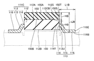
(半導体装置111A)
図1を参照して、本実施の形態における半導体装置111Aは、プリント配線板100の表面に実装されるいわゆる表面実装型の半導体装置であり、たとえばプラスティックパッケージのQFPである。
(
Referring to FIG. 1, a
半導体装置111Aは、本体112と複数の電極端子113とを備えている。本体112は、外周が略直方体に成型された絶縁性のモールド樹脂から構成されている。絶縁性のモールド樹脂とは、たとえばガラス粒が充填されたエポキシ樹脂である。本体112におけるモールド樹脂は、半導体素子(図示せず)、およびこの半導体素子と電極端子113(電極端子113におけるインナーリード部)とを接続するボンディングワイヤ(図示せず)等を内部に封止している。
The
本体112は、上面112A、下面112B、および側面112Sを有している。側面112Sの高さ方向(紙面上下方向)の中心の位置には、中央部112CAが規定されている。換言すると、中央部112CAから側面112Sの上端112Tまでの寸法HAと、中央部112CAから側面112Sの下端112Uまでの寸法HAとは等しくなっている。
The
各電極端子113は本体112の周囲(側面112Sに関する周囲)に並んで配設され、本体112の側面112Sから、本体112に対して外側に向かって突出している。各電極端子113はたとえば銅から構成されている。各電極端子113の表面には良好なはんだ付けを得るために錫めっき処理が施されているとよい。
Each
各電極端子113は、突出部114、延在部115、および水平部116を有している。突出部114の一端(インナーリード部)は、本体112の内部に含まれており、ボンディングワイヤによって半導体素子と電気的に接続されている。突出部114の他端(先端側)は、本体112の側面112Sから、本体112の上面112Aと平行な方向に突出している。
Each
突出部114の先端から、本体112の下面112B側に向かって延在部115が垂れ下がるように延在している。延在部115は、突出部114の先端から垂れ下がりつつ、下面112Bの本体112に対する外側に向かって傾斜している。
An extending
延在部115の先端から、本体112とは反対側(本体112に対するさらに外側)に向かって水平部116が延びている。水平部116は、本体112の上面112Aと平行な方向に延びている。水平部116の下面116Bは、本体112の下面112Bよりも下方側(紙面下側)に位置している。
A
本体112および電極端子113の各寸法等はたとえば次の通りである。本体112の図1紙面左右方向における幅は約20mm〜約40mmである。本体112の高さ(図1における寸法HA+寸法HAの値)は約1mm〜約2mmである。電極端子113の図1紙面上下方向における厚さは、約0.1mm〜約0.15mmである。電極端子113の図1紙面垂直方向における幅(図3における幅R1参照)は、約0.2mmである。隣り合う電極端子113の間隔(図3における間隔R2参照)は、約0.2mmである。
The dimensions and the like of the
ここで、幅方向(図1紙面左右方向)において、水平部116の先端116Eと本体112の側面112Sにおける上端112Tとの間には、寸法L1Aが規定されている。高さ方向(図1紙面上下方向)において、水平部116の下面116Bと側面112Sの上端112Tとの間には寸法L2Aが規定されている。寸法L2Aは、寸法L1A以上となっている(L2A≧L1A)。
Here, in the width direction (left and right direction in FIG. 1), a dimension L1A is defined between the
さらに、突出部114の上面114Tは、本体112の側面112Sにおける中央部112CAよりも、本体112の下面112B側に位置している。
Furthermore, the
(半導体装置111Aの実装方法)
図2〜図9を参照して、本実施の形態における半導体装置111Aの実装方法について説明する。図2〜図9は、この実装方法における各工程を経時的に示している。この実装方法は、フローはんだ付け法であれば、静止槽方式(DIP方式)および噴流方式(フロー方式)の2つの方式のいずれであってもよい。この実装方法について、ここでは静止槽方式(DIP方式)に基づいて説明する。
(Method of mounting
With reference to FIGS. 2 to 9, a mounting method of the
図2および図3を参照して、この実装方法においては、プリント配線板100と上述の半導体装置111Aとが準備される。
Referring to FIGS. 2 and 3, in this mounting method, printed
プリント配線板100は、たとえばガラスエポキシ性の配線基材101を有している。配線基材101における半導体装置111Aが実装される表面には、配線導体102および配線電極104が形成されている。配線導体102および配線電極104の図2紙面上下方向における厚さは、たとえば約50μmである。
The printed
配線導体102および配線電極104は、銅箔等をエッチングすることによりパターニングされている。配線電極104は、配線導体102に電気的に繋がっている。プリント配線板100の表面にはソルダレジスト103が形成されている。ソルダレジスト103は絶縁性を有する表面部材の一例であり、たとえばエポキシ樹脂から構成される。ソルダレジスト103は、余分なはんだが配線導体102に付着しないように配線導体102を覆っている。
The
ソルダレジスト103には、配線電極104が露出するように平面視矩形状(図3参照)の開口(開口部103a〜開口部103b)が形成されている。平面視において、この開口(開口部103a〜開口部103b)の形状は、半導体装置111Aにおける電極端子113の水平部116(図1参照)の形状よりも大きい。平面視において、この開口は電極端子113の水平部116を含むことが可能となっている。矢印AR1に示すように、半導体装置111Aはプリント配線板100の表面に載置される。
The solder resist 103 is formed with openings (opening
図4を参照して、半導体装置111Aは、プリント配線板100の表面に載置された後、所定の接着材(図示せず)によってプリント配線板100に仮固定される。開口部103bは、半導体装置111Aがプリント配線板100の表面に仮固定された状態において、電極端子113の先端116Eよりも幅方向(図4紙面左右方向)の外側に位置している。この状態においては、電極端子113の水平部116と配線電極104とは接触していてもよく(図4に示す状態)、わずかな隙間を空けて図4紙面上下方向に離間していてもよい。
Referring to FIG. 4,
図5を参照して、はんだ槽(図示せず)内に貯留された溶融はんだ131が準備される。溶融はんだ131は、たとえば、Sn−3.0Ag−0.5Cuの組成比を有する鉛フリーはんだ合金である。溶融はんだ131の溶融温度はたとえば約250℃である。
Referring to FIG. 5,
プリント配線板100の半導体装置111Aが仮固定されている側の表面を下方にした状態で、半導体装置111Aはその上面側から溶融はんだ131に浸漬される。半導体装置111Aは、溶融はんだ131の表面に対して垂直に浸漬されてもよく、溶融はんだ131の表面に対して斜めに浸漬されてもよい。
With the surface of the printed
図6〜図8を参照して、半導体装置111Aが溶融はんだ131に浸漬されたときの、半導体装置111Aの周囲に位置する溶融はんだ131の経時的な変化について説明する。
With reference to FIG. 6 to FIG. 8, changes with time of the
図6を参照して、半導体装置111Aが溶融はんだ131に浸漬された直後では、溶融はんだ131の表面131Sは、本体112に上方から押さえ付けられるようにして下方に下がる。
Referring to FIG. 6, immediately after
溶融はんだ131の表面131Sは、図6に示すような曲率半径の小さな曲面形状(比較例と対比し、詳細は後述する)を呈する。溶融はんだ131の強い表面張力によって、溶融はんだ131の表面131Sは、半導体装置111Aの外形形状に沿う(半導体装置111Aの表面をなぞるように濡れ広がる)ことはない。
The
ここで、半導体装置111Aにおいては上述のとおり(図1参照)、寸法L2Aは寸法L1A以上となっており、且つ突出部114の上面114Tは本体112の側面112Sにおける中央部112CAよりも本体112の下面112B側に位置している。当該構成によって、半導体装置111Aが溶融はんだ131に浸漬された直後において、溶融はんだ131は電極端子113に接触することはない。
Here, in the
溶融はんだ131は、電極端子113よりも外側に位置する配線電極104に、電極端子113よりも先に接触する(接触端141を参照)。溶融はんだ131と配線電極104との接触端141に濡れが生じる。この濡れにより、接触端141は本体112に徐々に近づく(矢印AR2方向)。
The
図7を参照して、接触端141の移動に伴って、溶融はんだ131は電極端子113の先端に接触する(接触端142を参照)。溶融はんだ131と電極端子113との接触端142にも濡れが生じる。この濡れにより、接触端142は本体112に近づく(矢印AR3方向)。
Referring to FIG. 7, as the
図8を参照して、接触端142が本体112に近づくことによって、電極端子113と配線電極104との間(およびこれらの周辺)に所定量の溶融はんだ131が供給される。この状態に到達した後、半導体装置111Aおよびプリント配線板100は溶融はんだ131から引き抜かれる。半導体装置111Aが溶融はんだ131に浸漬されてから、半導体装置111Aが溶融はんだ131から引き抜かれるまでの時間は、たとえば2秒〜3秒である。電極端子113と配線電極104との間(およびこれらの周辺)に供給された溶融はんだ131は、その温度が低下することによって凝固する。
Referring to FIG. 8, when
図9を参照して、溶融はんだ131から引き抜かれたプリント配線板100においては、電極端子113が、凝固したはんだ132によって配線電極104に接合されている。この接合により、半導体装置111Aはプリント配線板100に実装される。
Referring to FIG. 9, in printed
(作用・効果)
半導体装置111Aが溶融はんだ131に浸漬された直後において、溶融はんだ131は電極端子113に接触することがない(図6参照)。換言すると、浸漬直後においては、電極端子113には溶融はんだ131が供給されない。溶融はんだ131は、電極端子113よりも外側に位置する配線電極104に、電極端子113よりも先に接触する。電極端子113には、プリント配線板100の配線電極104に生じる濡れを通して溶融はんだ131が徐々に供給される(図7から図8に示す状態)。
(Action / Effect)
Immediately after the
半導体装置111Aにおいては、電極端子113への溶融はんだ131の供給量が少なくなるように調整されている(比較例と対比し、詳細は後述する)。隣り合う電極端子113同士の間への溶融はんだ131の供給量も少なくなる。電極端子113と配線電極104との間(およびこれらの周辺)に所定量の溶融はんだ131が供給された後、半導体装置111Aおよびプリント配線板100は溶融はんだ131から引き抜かれる。
In the
隣り合う電極端子113同士の間への溶融はんだ131の供給量が少なくなるように調整されることによって、隣り合う電極端子113間におけるブリッジの発生が抑制される。結果として、隣り合う電極端子113間における短絡の発生も抑制されることが可能となる。
By adjusting the supply amount of the
半導体装置111Aが溶融はんだに浸漬されてから、半導体装置111Aが溶融はんだ131から引き抜かれるまでの時間については、半導体装置111Aの本体112の大きさ、電極端子113の幅R1(図3参照)、または隣り合う電極端子113の間隔R2(図3参照)等に応じて、良好なはんだ付けが得られ、且つブリッジの発生が抑制されるように最適化されるとよい。
Regarding the time from when the
上述の各寸法L1A,L2A(図1参照)、および本体112および電極端子113の各寸法等についても、半導体装置111Aが溶融はんだ131に浸漬された直後において溶融はんだ131が電極端子113に接触せず、且つ、配線電極104に電極端子113よりも先に接触した溶融はんだ131が電極端子113に向かって良好に濡れ広がるように最適化されるとよい。
Regarding the above dimensions L1A and L2A (see FIG. 1) and the dimensions of the
以上述べたとおり、半導体装置111Aによれば、フローはんだ付け法によっても、隣り合う電極端子113間における短絡の発生が抑制され、プリント配線板100に良好に実装されることが可能となる。半導体装置111Aの実装方法によれば、フローはんだ付け法によっても、隣り合う電極端子113間における短絡の発生が抑制され、半導体装置111Aをプリント配線板100に良好に実装することが可能となる。
As described above, according to the
[比較例]
図10を参照して、半導体装置111Zについて説明する。半導体装置111Zは、上述の実施の形態1における半導体装置111Aに対する比較例である。図10は、半導体装置111Zを溶融はんだ131に浸漬した直後の様子を示す断面図である。
[Comparative example]
The
半導体装置111Zにおいては、幅方向(図10紙面左右方向)において、水平部116の先端と本体112の側面における上端との間に寸法L1Zが規定されている。高さ方向(図10紙面上下方向)において、水平部116の下面と側面の上端との間に寸法L2Zが規定されている。半導体装置111Zにおいては、寸法L2Zは、寸法L1Z以上とはなっていない(L2Z<L1Z)。
In the
さらに、半導体装置111Zにおいては、突出部114の上面は、本体112の側面における中央部よりも、本体112の下面側(紙面上方側)には位置していない。
Further, in the
半導体装置111Zが溶融はんだ131に浸漬された直後では、溶融はんだ131の表面131Sは、本体112に上方から押さえられるようにして下方に下がる。
Immediately after the
半導体装置111Zにおいては、溶融はんだ131の表面131Sは、図10に示すような曲率半径の大きな曲面形状を呈する。比較例における表面131Sは、上述の実施の形態1における表面131S(図5参照)に比べてなだらかな曲面を呈している。
In the
半導体装置111Zが溶融はんだ131に浸漬された直後において、溶融はんだ131は、配線電極104だけでなく電極端子113にも既に接触している(接触端142を参照)。溶融はんだ131と電極端子113との接触端142に濡れが生じる。この濡れによって、電極端子113と配線電極104との間(およびこれらの周辺)には、上述の実施の形態1に比べて多くの量の溶融はんだ131が浸漬直後において供給される。浸漬直後において既に電極端子113と配線電極104との間に溶融はんだ131が供給されているため、本比較例における半導体装置111Zにおいては、電極端子113への溶融はんだ131の供給量が調整されることはできない状態となっている。
Immediately after the
半導体装置111Zが溶融はんだ131から引き抜かれたとき、隣り合う電極端子113間への溶融はんだ131の供給量が多いため、隣り合う電極端子113間における溶融はんだ131は、はんだ槽(図示せず)に戻らずに残留する。残留した溶融はんだ131によって、ブリッジが発生する。結果として、半導体装置111Zによれば、隣り合う電極端子113間における短絡が発生してしまう。
When the
一方、上述の実施の形態1における半導体装置111A(図5参照)によれば、寸法L1A,L2Aおよび電極端子113の突出部114の上面114Tの位置が上記のとおり設定されている。この考慮によって、半導体装置111Aが溶融はんだ131に浸漬された直後において、溶融はんだ131は電極端子113に接触しない状態が実現されている。
On the other hand, according to the
その結果、上述の実施の形態1における半導体装置111Aによれば、電極端子113への溶融はんだ131の供給量が少なくなるように調整されることが可能とされている。電極端子113には、プリント配線板100の配線電極104に生じる濡れを通して溶融はんだ131は徐々に供給される。隣り合う電極端子113同士の間への溶融はんだ131の供給量が少なくなるように調整されることによって、隣り合う電極端子113間におけるブリッジの発生が抑制される。結果として、隣り合う電極端子113間における短絡の発生も抑制されることが可能となる。
As a result, according to the
[実施の形態1の他の構成]
図11を参照して、実施の形態1の他の構成における半導体装置111Aa、および半導体装置111Aaの実装方法について説明する。ここでは上述の実施の形態1との相違点について説明する。
[Other configuration of the first embodiment]
With reference to FIG. 11, a semiconductor device 111Aa and a mounting method of the semiconductor device 111Aa in another configuration of the first embodiment will be described. Here, differences from the above-described first embodiment will be described.
半導体装置111Aaは、複数の仕切部120をさらに備えている。仕切部120は、隣り合う電極端子113同士の間を空間的に仕切るように配設され、絶縁性および溶融はんだ131(図5参照)に対して非濡れ性を有している。ここでいう非濡れ性とは、溶融はんだ131と金属的な結合反応を起こさない性質を意味する。
The semiconductor device 111Aa further includes a plurality of
各仕切部120は、たとえばガラス粒が充填されたエポキシ樹脂によって平板状に構成される。各仕切部120は、本体112と一体的に成型されているとよい。各仕切部120は、本体112とは別体に成型され、成型後に本体112に接合されてもよい。
Each
半導体装置111Aaは、上述の実施の形態1と同様に、溶融はんだ131(図5参照)に浸漬された後、溶融はんだ131から引き抜かれる。仕切部120が隣り合う電極端子113同士の間を空間的に仕切っていることによって、溶融はんだ131の流動による隣り合う電極間における短絡の発生がより抑制されることが可能となる。
The
各仕切部120は、隣り合う電極端子113同士の間を完全に仕切るように構成されていても、隣り合う電極端子113同士の間を部分的に仕切るように構成されていてもよい。ここで言う部分的にとは、たとえば仕切部120の先端側の一部が、電極端子113の先端側から本体112側に向かって後退するように構成されていることである。
Each
各仕切部120が隣り合う電極端子113同士の間を部分的に仕切っている場合であっても、半導体装置111Aaが浸漬される溶融はんだ131の表面張力によって、隣り合う電極端子113同士の間には溶融はんだ131は供給されない。結果として、この場合であっても溶融はんだ131の流動による隣り合う電極間における短絡の発生がより抑制されることが可能となる。
Even when each
各仕切部120は、絶縁性および溶融はんだ131に対して非濡れ性を有している材質であれば、ポリイミド等の樹脂であってもよく、アルミナ等のセラミックであってもよい。
Each
[実施の形態2]
図12〜図14を参照して、本実施の形態について説明する。
[Embodiment 2]
The present embodiment will be described with reference to FIGS.
(半導体装置111B)
図12を参照して、本実施の形態における半導体装置111Bは、プリント配線板100の表面に実装されるいわゆる表面実装型の半導体装置であり、たとえばプラスティックパッケージのQFPである。
(
Referring to FIG. 12,
半導体装置111Bは、本体112と複数の電極端子113とを備えている。本体112は、(後述する張出部117が設けられている部分を除いて)外周が略直方体に成型された絶縁性のモールド樹脂から構成されている。
The
各電極端子113は、上述の実施の形態1における半導体装置111Aの各電極端子113と同様に、本体112の周囲(側面112Sに関する周囲)に並んで配設され、本体112の側面112Sから、本体112に対して外側に向かって突出している。
Similar to each
半導体装置111Bにおいては、本体112の側面112Sから幅方向(図12紙面左右方向)外側に向かってフランジ状に張り出す張出部117が本体112に設けられている。張出部117は平板状に構成され、その外形は平面視正方形となっている。張出部117は、電極端子113の上方を含むように位置している。
In the
張出部117は、たとえばガラス粒が充填されたエポキシ樹脂から構成される。張出部117は、本体112と一体的に成型されているとよい。張出部117は、本体112とは別体に成型され、成型後に本体112に接合されてもよい。張出部117が本体112とは別体に成型される場合、張出部117は溶融はんだ131(図5参照)に対して非濡れ性を有している材質であれば、ポリイミド等の樹脂であってもよく、アルミナ等のセラミックであってもよい。
The overhanging
ここで、幅方向(図12紙面左右方向)において、張出部117の先端117Tは、電極端子113の水平部116の先端116Eよりも本体112側に位置している。換言すると、幅方向(図12紙面左右方向)において、側面112Sから水平部116の先端116Eまでの寸法113Rは、側面112Sから張出部117の先端117Tまでの寸法117Rより小さい(117R<113R)。
Here, in the width direction (left and right direction in FIG. 12), the
好適には、張出部117の先端117Tを水平部116側(図12紙面下側)に投影したときに得られる先端117Tに対応する投影像(投影点)の位置は、水平部116が設けられている領域116R内に含まれているとよい。
Preferably, the position of the projection image (projection point) corresponding to the
(半導体装置111Bの実装方法)
図13および図14を参照して、本実施の形態における半導体装置111Bの実装方法について説明する。図13および図14は、この実装方法における各工程の一部を経時的に示している。この実装方法は、フローはんだ付け法であれば、静止槽方式(DIP方式)および噴流方式(フロー方式)の2つの方式のいずれであってもよい。この実装方法について、ここでは静止槽方式(DIP方式)に基づいて説明する。
(Method of mounting
With reference to FIGS. 13 and 14, a mounting method of
図13を参照して、この実装方法においては、上述の実施の形態1と同様なプリント配線板100と、上述の半導体装置111Bとが準備される。半導体装置111Bは、プリント配線板100の表面に仮固定される。
Referring to FIG. 13, in this mounting method, printed
図14を参照して、上述の実施の形態1と同様な溶融はんだ131が準備される。プリント配線板100の半導体装置111Bが仮固定されている側の表面を下方にした状態で、半導体装置111Bはその上面側から溶融はんだ131に浸漬される。
Referring to FIG. 14, a
半導体装置111Bが溶融はんだ131に浸漬された直後では、溶融はんだ131の表面131Sは、本体112に上方から押さえ付けられるようにして下方に下がる。
Immediately after the
溶融はんだ131の強い表面張力、およびフランジ状に張り出す張出部117が本体112に設けられていることによって、溶融はんだ131の表面131Sは、半導体装置111Bの外形形状に沿う(半導体装置111Bの表面をなぞるように濡れ広がる)ことはない。半導体装置111Bが溶融はんだ131に浸漬された直後において、溶融はんだ131は電極端子113に接触することがない。
By providing the
溶融はんだ131は、電極端子113よりも外側に位置する配線電極104に、電極端子113よりも先に接触する(接触端141を参照)。溶融はんだ131と配線電極104との接触端141に濡れが生じる。この濡れにより、接触端141は本体112に徐々に近づく(矢印AR4方向)。
The
接触端141の移動に伴って、溶融はんだ131は電極端子113の先端に接触する。この接触により、溶融はんだ131と電極端子113との間に濡れが生じる。この濡れにより、電極端子113と配線電極104との間(およびこれらの周辺)に所定量の溶融はんだ131が供給される。この状態に到達した後、半導体装置111Bおよびプリント配線板100は溶融はんだ131から引き抜かれる。
As the
電極端子113と配線電極104との間(およびこれらの周辺)に供給された溶融はんだ131は、その温度が低下することによって凝固する。こうして、半導体装置111Bはプリント配線板100に実装される。
The
(作用・効果)
半導体装置111Bが溶融はんだ131に浸漬された直後において、溶融はんだ131は電極端子113に接触することがない(図14参照)。換言すると、浸漬直後においては、電極端子113には溶融はんだ131が供給されない。溶融はんだ131は、電極端子113よりも外側に位置する配線電極104に、電極端子113よりも先に接触する。電極端子113には、プリント配線板100の配線電極104に生じる濡れを通して溶融はんだ131が徐々に供給される。
(Action / Effect)
Immediately after the
半導体装置111Bにおいては、電極端子113への溶融はんだ131の供給量が少なくなるように調整されている。隣り合う電極端子113同士の間への溶融はんだ131の供給量も少なくなる。電極端子113と配線電極104との間(およびこれらの周辺)に所定量の溶融はんだ131が供給された後、半導体装置111Bおよびプリント配線板100は溶融はんだ131から引き抜かれる。
In the
隣り合う電極端子113同士の間への溶融はんだ131の供給量も少なくなることによって、隣り合う電極端子113間におけるブリッジの発生が抑制される。結果として、隣り合う電極端子113間における短絡の発生も抑制されることが可能となる。
Since the supply amount of the
以上述べたとおり、半導体装置111Bによれば、フローはんだ付け法によっても、隣り合う電極端子113間における短絡の発生が抑制され、プリント配線板100に良好に実装されることが可能となる。半導体装置111Bの実装方法によれば、フローはんだ付け法によっても、隣り合う電極端子113間における短絡の発生が抑制され、半導体装置111Bをプリント配線板100に良好に実装することが可能となる。
As described above, according to the
[実施の形態2の他の構成]
図15を参照して、実施の形態2の他の構成における半導体装置111Ba、および半導体装置111Baの実装方法について説明する。ここでは上述の実施の形態2との相違点について説明する。
[Other configurations of the second embodiment]
With reference to FIG. 15, a semiconductor device 111Ba and a mounting method of the semiconductor device 111Ba in another configuration of the second embodiment will be described. Here, differences from the second embodiment will be described.
半導体装置111Baは、上述の実施の形態1の他の構成と同様な、複数の仕切部120をさらに備えている。
The semiconductor device 111Ba further includes a plurality of
半導体装置111Baは、上述の実施の形態2と同様に、溶融はんだ131(図14参照)に浸漬された後、溶融はんだ131から引き抜かれる。仕切部120が隣り合う電極端子113同士の間を空間的に仕切っていることによって、溶融はんだ131の流動による隣り合う電極間における短絡の発生がより抑制されることが可能となる。
The semiconductor device 111Ba is pulled out of the
各仕切部120は、隣り合う電極端子113同士の間を完全に仕切るように構成されていても、隣り合う電極端子113同士の間を部分的に仕切るように構成されていてもよい。
Each
[実施の形態3]
図16および図17を参照して、実施の形態3における半導体装置111Bb、および半導体装置111Bbの実装方法について説明する。ここでは、上述の実施の形態2との相違点について説明する。
[Embodiment 3]
With reference to FIG. 16 and FIG. 17, the semiconductor device 111Bb and the mounting method of the semiconductor device 111Bb in the third embodiment will be described. Here, differences from the second embodiment will be described.
半導体装置111Bbにおける張出部117には、張出部117を厚さ方向に貫通する複数の貫通孔117Hが設けられている。各貫通孔117Hの位置は、各電極端子113の位置に対応している。各貫通孔117Hは、各電極端子113の上方の一部を含んでいる。平面視において、各貫通孔117Hは各電極端子113の長手方向の一部を含んでいる。各貫通孔117Hの形状は、平面視矩形状であってもよく、平面視円形状等であってもよい。
The overhanging
半導体装置111Bbの製造時において、細径のピン状部材(プレス治具)(図示せず)を貫通孔117Hの上方から下方に向かって通過させる。ピン状部材によるプレス加工によって、電極端子113を容易に曲げることが可能となる。
At the time of manufacturing the semiconductor device 111Bb, a small-diameter pin-shaped member (press jig) (not shown) is passed downward from above the through
(実施の形態3の他の構成)
図18を参照して、実施の形態3の他の構成としての半導体装置111Bcのように、上述の実施の形態2の他の構成(図15参照)と同様な複数の仕切部120が、隣り合う電極端子113同士の間を空間的に仕切るように配設されていてもよい。
(Other configuration of the third embodiment)
Referring to FIG. 18, like a
(実施の形態3のさらに他の構成)
図19を参照して、実施の形態3のさらに他の構成としての半導体装置111Bdのように、貫通孔117Hは2以上の電極端子113を平面視において跨ぐように、長孔状に形成されていてもよい。図19に示す態様において、図18のような複数の仕切部120(図19において図示せず)がさらに配設されていてもよい。
(Still another configuration of the third embodiment)
Referring to FIG. 19, as in the semiconductor device 111Bd as still another configuration of the third embodiment, the through
[実施の形態4]
図20〜図22を参照して、本実施の形態について説明する。
[Embodiment 4]
The present embodiment will be described with reference to FIGS.
(半導体装置111C)
図20を参照して、本実施の形態における半導体装置111Cは、プリント配線板100の表面に実装されるいわゆる表面実装型の半導体装置であり、たとえばプラスティックパッケージのQFPである。
(
Referring to FIG. 20,
半導体装置111Cは、本体112と複数の電極端子113とを備えている。本体112は、外周が略直方体に成型された絶縁性のモールド樹脂から構成されている。各電極端子113は、上述の実施の形態1における半導体装置111Aの各電極端子113と同様に、本体112の周囲(側面112Sに関する周囲)に並んで配設され、本体112の側面112Sから、本体112に対して外側に向かって突出している。
The
(半導体装置111Cの実装方法)
本実施の形態における半導体装置111Cの実装方法について説明する。この実装方法は、フローはんだ付け法であれば、静止槽方式(DIP方式)および噴流方式(フロー方式)の2つの方式のいずれであってもよい。この実装方法について、ここでは静止槽方式(DIP方式)に基づいて説明する。
(Method for mounting
A mounting method of the
図21を参照して、この実装方法においては、上述の実施の形態1と同様なプリント配線板100と、上述の半導体装置111Cと、実装用治具150とが準備される。半導体装置111Cは、プリント配線板100の表面に仮固定される。
Referring to FIG. 21, in this mounting method, printed
実装用治具150は、上面150Aおよび下面150Bを有する平板状のたとえば耐熱性を有するエポキシ樹脂であり、溶融はんだ131(図22参照)に対して非濡れ性を有している。
The mounting
実装用治具150は、本体112の上面112A(図20参照)と実装用治具150の下面150B(図20参照)とが接するように、本体112にたとえば接着剤(図示せず)等によって取り付けられる。
The mounting
図20を再び参照して、実装用治具150が本体112に取り付けられた状態において、本体112の側面112Sおよび実装用治具150の側面150Sを合算した高さ寸法における高さ方向(紙面上下方向)の中心の位置には、中央部112CBが規定されている。換言すると、中央部112CBから実装用治具150の側面150Sの上端150Tまでの寸法HBと、中央部112CBから本体112の側面112Sの下端112Uまでの寸法HBとは等しくなっている。
Referring again to FIG. 20, in the state where the mounting
幅方向(図20紙面左右方向)において、水平部116の先端116Eと実装用治具150の側面150Sにおける上端150Tとの間には、寸法L1Bが規定されている。高さ方向(図20紙面上下方向)において、水平部116の下面116Bと実装用治具150の側面150Sの上端150Tとの間には寸法L2Bが規定されている。寸法L2Bは、寸法L1B以上となっている(L2B≧L1B)。
In the width direction (left and right direction in FIG. 20), a dimension L1B is defined between the
さらに、突出部114の上面114Tは、上述の中央部112CBよりも、本体112の下面112B側に位置している。
Furthermore, the
図22を参照して、上述の実施の形態1と同様な溶融はんだ131が準備される。プリント配線板100の半導体装置111Cが仮固定されている側の表面を下方にした状態で、半導体装置111Cはその上面側(実装用治具150が取り付けられている側)から溶融はんだ131に浸漬される。
Referring to FIG. 22,
半導体装置111Cが溶融はんだ131に浸漬された直後では、溶融はんだ131の表面131Sは、実装用治具150に上方から押さえ付けられるようにして下方に下がる。
Immediately after the
溶融はんだ131の強い表面張力、および実装用治具150が本体112に取り付けられていることによって、溶融はんだ131の表面131Sは、半導体装置111Cの外形形状に沿う(半導体装置111Cの表面をなぞるように濡れ広がる)ことはない。半導体装置111Cが溶融はんだ131に浸漬された直後において、溶融はんだ131は電極端子113に接触することがない。
Due to the strong surface tension of the
溶融はんだ131は、電極端子113よりも外側に位置する配線電極104に、電極端子113よりも先に接触する(接触端141を参照)。溶融はんだ131と配線電極104との接触端141に濡れが生じる。この濡れにより、接触端141は本体112に徐々に近づく(矢印AR5方向)。
The
接触端141の移動に伴って、溶融はんだ131は電極端子113の先端に接触する。この接触により、溶融はんだ131と電極端子113との間に濡れが生じる。この濡れにより、電極端子113と配線電極104との間(およびこれらの周辺)に所定量の溶融はんだ131が供給される。この状態に到達した後、半導体装置111Cおよびプリント配線板100は、実装用治具150とともに溶融はんだ131から引き抜かれる。
As the
電極端子113と配線電極104との間(およびこれらの周辺)に供給された溶融はんだ131は、その温度が低下することによって凝固する。こうして、半導体装置111Cはプリント配線板100に実装される。この実装後、実装用治具150は本体112から取り外されるように構成してもよい。
The
(作用・効果)
半導体装置111Cが溶融はんだ131に浸漬された直後において、溶融はんだ131は電極端子113に接触することがない(図22参照)。換言すると、浸漬直後においては、電極端子113には溶融はんだ131が供給されない。溶融はんだ131は、電極端子113よりも外側に位置する配線電極104に、電極端子113よりも先に接触する。電極端子113には、プリント配線板100の配線電極104に生じる濡れを通して溶融はんだ131が徐々に供給される。
(Action / Effect)
Immediately after the
半導体装置111Cにおいては、電極端子113への溶融はんだ131の供給量が少なくなるように調整されている。隣り合う電極端子113同士の間への溶融はんだ131の供給量も少なくなる。電極端子113と配線電極104との間(およびこれらの周辺)に所定量の溶融はんだ131が供給された後、半導体装置111Cおよびプリント配線板100は実装用治具150とともに溶融はんだ131から引き抜かれる。
In the
隣り合う電極端子113同士の間への溶融はんだ131の供給量が少なくなるように調整されることによって、隣り合う電極端子113間におけるブリッジの発生が抑制される。結果として、隣り合う電極端子113間における短絡の発生も抑制されることが可能となる。
By adjusting the supply amount of the
以上述べたとおり、実装用治具150を用いた半導体装置111Cの実装方法によれば、フローはんだ付け法によっても、隣り合う電極端子113間における短絡の発生が抑制され、半導体装置111Cをプリント配線板100に良好に実装することが可能となる。半導体装置111Cの本体112の大きさに特別な寸法条件などを要求せずとも、実装用治具150によって上記の式(L2B≧L1B)などを満足するように構成するとよい。
As described above, according to the mounting method of the
(実施の形態4の他の構成)
図23を参照して、実施の形態4の他の構成としての半導体装置111Caのように、上述の実施の形態1の他の構成(図11参照)と同様な複数の仕切部120が、隣り合う電極端子113同士の間を空間的に仕切るように配設されていてもよい。仕切部120は、本体112に一体的に設けられていてもよく、実装用治具150から垂れ下がるように実装用治具150に一体的に設けられていてもよい。
(Other configuration of the fourth embodiment)
Referring to FIG. 23, like a semiconductor device 111Ca as another configuration of the fourth embodiment, a plurality of
[実施の形態5]
図24〜図26を参照して、本実施の形態について説明する。
[Embodiment 5]
The present embodiment will be described with reference to FIGS.
(半導体装置111D)
図24を参照して、本実施の形態における半導体装置111Dは、プリント配線板100の表面に実装されるいわゆる表面実装型の半導体装置であり、たとえばプラスティックパッケージのQFPである。
(
Referring to FIG. 24,
半導体装置111Dは、本体112と複数の電極端子113とを備えている。本体112は、外周が略直方体に成型された絶縁性のモールド樹脂から構成されている。各電極端子113は、上述の実施の形態1における半導体装置111Aの各電極端子113と同様に、本体112の周囲(側面112Sに関する周囲)に並んで配設され、本体112の側面112Sから、本体112に対して外側に向かって突出している。
The
(半導体装置111Dの実装方法)
本実施の形態における半導体装置111Dの実装方法について説明する。この実装方法は、フローはんだ付け法であれば、静止槽方式(DIP方式)および噴流方式(フロー方式)の2つの方式のいずれであってもよい。この実装方法について、ここでは静止槽方式(DIP方式)に基づいて説明する。
(Method for mounting
A method for mounting the
図25を参照して、この実装方法においては、上述の実施の形態1と同様なプリント配線板100と、上述の半導体装置111Dと、実装用治具150とが準備される。半導体装置111Dは、プリント配線板100の表面に仮固定される。
Referring to FIG. 25, in this mounting method, printed
実装用治具150は、上面150Aおよび下面150Bを有する平板状のたとえば耐熱性を有するエポキシ樹脂であり、溶融はんだ131(図26参照)に対して非濡れ性を有している。
The mounting
実装用治具150は、本体112の上面112A(図24参照)と実装用治具150の下面150B(図24参照)とが接するように、本体112にたとえば接着剤(図示せず)等によって取り付けられる。
The mounting
図24を再び参照して、実装用治具150は、張出部118を有している。実装用治具150が本体112に取り付けられた状態において、張出部118は、本体112の側面112S上方から幅方向(図24紙面左右方向)外側に向かってフランジ状に張り出している。張出部118は平板状に構成され、その外形は平面視正方形となっている。張出部118は、電極端子113の上方を含むように位置している。
Referring to FIG. 24 again, the mounting
ここで、幅方向(図24紙面左右方向)において、張出部118の先端118Tは、電極端子113の水平部116の先端116Eよりも本体112側に位置している。換言すると、幅方向(図24紙面左右方向)において、側面112Sから水平部116の先端116Eまでの寸法113Rは、側面112Sから張出部118の先端118Tまでの寸法118Rより小さい(118R<113R)。
Here, in the width direction (left and right direction in FIG. 24), the
好適には、張出部118の先端118Tを水平部116側(図24紙面下側)に投影したときに得られる先端118Tに対応する投影像(投影点)の位置は、水平部116が設けられている領域116R内に含まれているとよい。
Preferably, the
図26を参照して、上述の実施の形態1と同様な溶融はんだ131が準備される。プリント配線板100の半導体装置111Dが仮固定されている側の表面を下方にした状態で、半導体装置111Dはその上面側(実装用治具150が取り付けられている側)から溶融はんだ131に浸漬される。
Referring to FIG. 26, a
半導体装置111Dが溶融はんだ131に浸漬された直後では、溶融はんだ131の表面131Sは、実装用治具150に上方から押さえ付けられるようにして下方に下がる。
Immediately after the
溶融はんだ131の強い表面張力、および実装用治具150が本体112に取り付けられていることによって、溶融はんだ131の表面131Sは、半導体装置111Dの外形形状に沿う(半導体装置111Dの表面をなぞるように濡れ広がる)ことはない。半導体装置111Dが溶融はんだ131に浸漬された直後において、溶融はんだ131は電極端子113に接触することがない。
Due to the strong surface tension of the
溶融はんだ131は、電極端子113よりも外側に位置する配線電極104に、電極端子113よりも先に接触する(接触端141を参照)。溶融はんだ131と配線電極104との接触端141に濡れが生じる。この濡れにより、接触端141は本体112に徐々に近づく(矢印AR6方向)。
The
接触端141の移動に伴って、溶融はんだ131は電極端子113の先端に接触する。この接触により、溶融はんだ131と電極端子113との間に濡れが生じる。この濡れにより、電極端子113と配線電極104との間(およびこれらの周辺)に所定量の溶融はんだ131が供給される。この状態に到達した後、半導体装置111Dおよびプリント配線板100は、実装用治具150とともに溶融はんだ131から引き抜かれる。
As the
電極端子113と配線電極104との間(およびこれらの周辺)に供給された溶融はんだ131は、その温度が低下することによって凝固する。こうして、半導体装置111Dはプリント配線板100に実装される。この実装後、実装用治具150は本体112から取り外されるように構成してもよい。
The
(作用・効果)
半導体装置111Dが溶融はんだ131に浸漬された直後において、溶融はんだ131は電極端子113に接触することがない(図26参照)。換言すると、浸漬直後においては、電極端子113には溶融はんだ131が供給されない。溶融はんだ131は、電極端子113よりも外側に位置する配線電極104に、電極端子113よりも先に接触する。電極端子113には、プリント配線板100の配線電極104に生じる濡れを通して溶融はんだ131が徐々に供給される。
(Action / Effect)
Immediately after the
半導体装置111Dにおいては、電極端子113への溶融はんだ131の供給量が少なくなるように調整されている。隣り合う電極端子113同士の間への溶融はんだ131の供給量も少なくなる。電極端子113と配線電極104との間(およびこれらの周辺)に所定量の溶融はんだ131が供給された後、半導体装置111Dおよびプリント配線板100は実装用治具150とともに溶融はんだ131から引き抜かれる。
In the
隣り合う電極端子113同士の間への溶融はんだ131の供給量が少なくなるように調整されることによって、隣り合う電極端子113間におけるブリッジの発生が抑制される。結果として、隣り合う電極端子113間における短絡の発生も抑制されることが可能となる。
By adjusting the supply amount of the
以上述べたとおり、実装用治具150を用いた半導体装置111Dの実装方法によれば、フローはんだ付け法によっても、隣り合う電極端子113間における短絡の発生が抑制され、半導体装置111Dをプリント配線板100に良好に実装することが可能となる。半導体装置111Cの本体112の大きさに特別な寸法条件などを要求せずとも、実装用治具150によって上記の式(118R<113R)などを満足するように構成するとよい。
As described above, according to the mounting method of the
(実施の形態5の他の構成)
図27を参照して、実施の形態5の他の構成としての、半導体装置111Daおよび実装用治具150のように、上述の実施の形態2の他の構成(図15参照)と同様な複数の仕切部121が、隣り合う電極端子113同士の間を仕切るように配設されていてもよい。仕切部121は、本体112に設けられていてもよく、実装用治具150から垂れ下がるように実装用治具150に一体的に設けられていてもよい。
(Other configuration of the fifth embodiment)
Referring to FIG. 27, a plurality of components similar to those in the other configuration of the second embodiment described above (see FIG. 15), such as semiconductor device 111Da and mounting
上述の実施の形態3における貫通孔117H(図16〜図18参照)と同様に、張出部118には複数の貫通孔118Hが設けられていてもよい。上述の実施の形態3における貫通孔117H(図19参照)と同様に、貫通孔118Hは、2以上の電極端子113を平面視において跨ぐように、長孔状に形成されていてもよい。
Similar to the through
以上、本発明に基づいた各実施の形態における半導体装置、半導体装置の実装方法、および実装用治具について説明したが、今回開示された各実施の形態はすべての点で例示であって制限的なものではないと考えられるべきである。 The semiconductor device, the semiconductor device mounting method, and the mounting jig in each embodiment based on the present invention have been described above. However, each embodiment disclosed this time is illustrative and restrictive in all respects. It should be considered not.
上述の各実施の形態においては、半導体装置がQFPである場合について説明したが、表面実装型の半導体装置であれば、SOP等であってもよい。上記の各実施の形態における半導体装置については、これらの半導体装置がフローはんだ付け方法によって実装されるという態様に基づき説明したが、上記の実施の形態1および実施の形態2(それぞれ他の構成を含む)における半導体装置としては、リフロー法によるはんだ付けによって実装されてもよい。 In each of the above-described embodiments, the case where the semiconductor device is a QFP has been described. However, an SOP or the like may be used if it is a surface-mount type semiconductor device. The semiconductor device in each of the above embodiments has been described based on an aspect in which these semiconductor devices are mounted by a flow soldering method. However, the above-described Embodiment 1 and Embodiment 2 (each having other configurations) The semiconductor device may be mounted by reflow soldering.
上述の各実施の形態においては、電極端子113への溶融はんだ131の供給量が少なくなるように調整されることによって、各半導体装置の溶融はんだ131への浸漬直後において、溶融はんだ131が電極端子113に接触しないという態様に基づいて説明した。電極端子113への溶融はんだ131の供給量が少なくなるように調整されることによって、各半導体装置の溶融はんだ131への浸漬直後において、溶融はんだ131が電極端子113にわずかに接触するように構成してもよい。この構成において、良好なはんだ付けが得られ、且つブリッジの発生が抑制されるように他の寸法等が最適化されるとよい。
In each of the above-described embodiments, by adjusting the supply amount of the
半導体装置の本体がエポキシ樹脂から構成される場合について説明したが、絶縁性を有する材料であれば、ポリイミド等他の樹脂であってもよく、アルミナ等のセラミックであってもよい。 Although the case where the main body of the semiconductor device is made of an epoxy resin has been described, other materials such as polyimide or ceramics such as alumina may be used as long as the material has insulating properties.
半導体装置の電極が銅から構成される場合について説明したが、42アロイ等他の金属材料であってもよい。半導体装置の電極には錫めっき処理が施されるとよいと述べたが、Sn−Pb合金めっき、Sn−BiまたはSn−Cuなどの錫系めっき、PdまたはAg等のめっきによる処理が施されていてもよく、ベンゾイミダゾール等の有機系の表面処理が施されていてもよい。 Although the case where the electrode of the semiconductor device is made of copper has been described, other metal materials such as 42 alloy may be used. The electrode of the semiconductor device is said to be subjected to a tin plating treatment, but a treatment by Sn-Pb alloy plating, tin-based plating such as Sn-Bi or Sn-Cu, or plating such as Pd or Ag is performed. Or an organic surface treatment such as benzimidazole.
溶融はんだとしてSn−3Ag−0.5Cuを用いる場合について説明したが、はんだであれば他の合金組成(スズ鉛はんだ)であってもよい。鉛フリーはんだの場合、溶融はんだの表面にはより強い表面張力を有する酸化膜が形成される。鉛フリーはんだを用いる場合の方が、スズ鉛はんだなどに比べて今回の発明の効果をより得ることができる。 Although the case where Sn-3Ag-0.5Cu is used as the molten solder has been described, other alloy compositions (tin lead solder) may be used as long as the solder is used. In the case of lead-free solder, an oxide film having a stronger surface tension is formed on the surface of the molten solder. In the case of using lead-free solder, the effect of the present invention can be obtained more than that of tin-lead solder.
実装用治具としては、耐熱性および溶融はんだに対して非濡れ性を有している材質であれば、ポリイミド等の樹脂であってもよく、アルミナ等のセラミックであってもよく、アルミニウム、ステンレスまたはチタンのように表面膜(不導体膜)を持つ金属であってもよい。ただし、アルミニウムなどのように熱伝導性が高い材質を採用すると、浸漬時に溶融はんだの熱が奪われるため熱伝導性が低いセラミック系、好ましくは樹脂系の材質が採用されるとよい。耐熱性の観点からは、樹脂系の中でもエポキシ系またはポリイミド系が好ましい。 As a mounting jig, as long as the material has heat resistance and non-wetting with respect to molten solder, it may be a resin such as polyimide, a ceramic such as alumina, aluminum, A metal having a surface film (nonconductive film) such as stainless steel or titanium may be used. However, if a material having high thermal conductivity such as aluminum is employed, the heat of the molten solder is taken away during immersion, and therefore a ceramic material, preferably a resin material, having low thermal conductivity may be employed. From the viewpoint of heat resistance, an epoxy system or a polyimide system is preferable among the resin systems.
したがって、本発明の範囲は特許請求の範囲によって示され、特許請求の範囲と均等の意味および範囲内でのすべての変更が含まれることが意図される。 Therefore, the scope of the present invention is defined by the terms of the claims, and is intended to include any modifications within the scope and meaning equivalent to the terms of the claims.
本発明は、電子部品を溶融はんだに浸漬することによりプリント配線板にはんだ付けされる電子回路装置に有効に利用される。 The present invention is effectively used in an electronic circuit device that is soldered to a printed wiring board by immersing the electronic component in molten solder.
100 プリント配線板、101 配線基材、102 配線導体、103 ソルダレジスト、103a,103b 開口部、104 配線電極、111A,111Aa,111B,111Ba,111Bb,111Bc,111Bd,111C,111Ca,111D,111Da,111Z 半導体装置、112 本体、112A,114T,150A 上面、112B,116B,150B 下面、112CA,112CB 中央部、112S,150S 側面、112T,150T 上端、112U 下端、113 電極端子、113R,117R,118R,HA,HB,L1A,L1B,L1Z,L2A,L2B,L2Z 寸法、114 突出部、115 延在部、116 水平部、116E,117T,118T 先端、116R 領域、117,118 張出部、117H,118H 貫通孔、120,121 仕切部、131 溶融はんだ、131S 表面、132 はんだ、141,142 接触端、150 実装用治具、AR1〜AR6,III 矢印、R1 幅、R2 間隔。 100 printed wiring board, 101 wiring substrate, 102 wiring conductor, 103 solder resist, 103a, 103b opening, 104 wiring electrode, 111A, 111Aa, 111B, 111Ba, 111Bb, 111Bc, 111Bd, 111C, 111Ca, 111D, 111Da, 111Z semiconductor device, 112 body, 112A, 114T, 150A top surface, 112B, 116B, 150B bottom surface, 112CA, 112CB center, 112S, 150S side surface, 112T, 150T top end, 112U bottom end, 113 electrode terminal, 113R, 117R, 118R, HA, HB, L1A, L1B, L1Z, L2A, L2B, L2Z Dimensions, 114 Projection, 115 Extension, 116 Horizontal, 116E, 117T, 118T Tip, 116R Region, 11 , 118 Overhang, 117H, 118H Through hole, 120, 121 Partition, 131 Molten solder, 131S surface, 132 Solder, 141, 142 Contact end, 150 Mounting jig, AR1 to AR6, III arrow, R1 width, R2 interval.
Claims (2)
半導体素子を内部に封止する本体と、A main body for sealing the semiconductor element inside;
前記本体の側面から突出する突出部、前記突出部の先端から前記本体の下面側に向かって延びる延在部、および、前記延在部の先端から前記本体とは反対側に向かって延びる水平部を有する複数の電極端子と、A protruding portion protruding from the side surface of the main body, an extending portion extending from the front end of the protruding portion toward the lower surface side of the main body, and a horizontal portion extending from the front end of the extending portion toward the opposite side of the main body A plurality of electrode terminals,
前記電極端子の上方に位置し、前記側面から幅方向外側に向かってフランジ状に張り出す張出部と、An overhanging portion located above the electrode terminal and projecting in a flange shape from the side surface toward the outside in the width direction;
を備え、With
前記張出部は、はんだに対して非濡れ性を有し、The overhanging portion has non-wetting property with respect to the solder,
幅方向において、前記張出部の先端は前記水平部の先端よりも前記本体側に位置し、In the width direction, the tip of the overhanging part is located closer to the main body than the tip of the horizontal part,
前記張出部は、前記張出部を厚さ方向に貫通する貫通孔を有し、The overhang portion has a through hole that penetrates the overhang portion in the thickness direction,
前記貫通孔は、前記電極端子の上方を含んでいる、The through hole includes an upper portion of the electrode terminal.
半導体装置。Semiconductor device.
請求項1に記載の半導体装置。The semiconductor device according to claim 1.
Priority Applications (1)
| Application Number | Priority Date | Filing Date | Title |
|---|---|---|---|
| JP2010135261A JP5590981B2 (en) | 2010-06-14 | 2010-06-14 | Semiconductor device |
Applications Claiming Priority (1)
| Application Number | Priority Date | Filing Date | Title |
|---|---|---|---|
| JP2010135261A JP5590981B2 (en) | 2010-06-14 | 2010-06-14 | Semiconductor device |
Publications (2)
| Publication Number | Publication Date |
|---|---|
| JP2012004179A JP2012004179A (en) | 2012-01-05 |
| JP5590981B2 true JP5590981B2 (en) | 2014-09-17 |
Family
ID=45535893
Family Applications (1)
| Application Number | Title | Priority Date | Filing Date |
|---|---|---|---|
| JP2010135261A Expired - Fee Related JP5590981B2 (en) | 2010-06-14 | 2010-06-14 | Semiconductor device |
Country Status (1)
| Country | Link |
|---|---|
| JP (1) | JP5590981B2 (en) |
Family Cites Families (8)
| Publication number | Priority date | Publication date | Assignee | Title |
|---|---|---|---|---|
| JPS6422039U (en) * | 1987-07-29 | 1989-02-03 | ||
| JPH0279052U (en) * | 1988-12-07 | 1990-06-18 | ||
| JPH0467346U (en) * | 1990-10-23 | 1992-06-15 | ||
| JPH053266A (en) * | 1991-06-25 | 1993-01-08 | Mitsubishi Electric Corp | Semiconductor device |
| JP2933105B2 (en) * | 1991-10-17 | 1999-08-09 | 富士通株式会社 | Semiconductor device |
| JPH0661378A (en) * | 1992-08-06 | 1994-03-04 | Nec Corp | Semiconductor device |
| JPH06252543A (en) * | 1993-03-01 | 1994-09-09 | Corona Denshi Kk | Method for soldering ic substrate |
| JP3286765B2 (en) * | 1993-03-09 | 2002-05-27 | 株式会社日立製作所 | Semiconductor device |
-
2010
- 2010-06-14 JP JP2010135261A patent/JP5590981B2/en not_active Expired - Fee Related
Also Published As
| Publication number | Publication date |
|---|---|
| JP2012004179A (en) | 2012-01-05 |
Similar Documents
| Publication | Publication Date | Title |
|---|---|---|
| JP2005095977A (en) | Circuit device | |
| JP2007141570A (en) | Mounting structure of female connector | |
| JP5881829B2 (en) | Method for packaging quad flat no-lead package body and package body | |
| JP4650948B2 (en) | Through-hole soldering structure | |
| JP2015188004A (en) | Package, semiconductor device, and semiconductor module | |
| JP2011243752A (en) | Semiconductor device manufacturing method, internal semiconductor connection member, and internal semiconductor connection member group | |
| CN105491816B (en) | Magnetic coil welding method | |
| JP5590981B2 (en) | Semiconductor device | |
| JP2009277777A (en) | Solder ball loading method and member for mounting electronic component | |
| JP2008294390A (en) | Module structure | |
| JPWO2008026335A1 (en) | Electronic component device and manufacturing method thereof, and electronic component assembly and manufacturing method thereof | |
| JP2008034514A (en) | Semiconductor device | |
| JP2013258013A (en) | Fuse | |
| JP2007335767A (en) | Component connecting terminal for semiconductor power module | |
| JP2004200539A (en) | Component-connecting terminal and electronic device | |
| JP2006114571A (en) | Semiconductor device and electronic apparatus provided therewith | |
| JP6025594B2 (en) | Terminal positioning jig | |
| JP2006269970A (en) | Solder joint method of electronic component | |
| JPH06296073A (en) | Flexible printed circuit board | |
| JP2010034168A (en) | Electronic component soldering method | |
| KR102775585B1 (en) | How to join weld plates on flexible circuit boards for batteries | |
| JP2004349413A (en) | Surface mounting clamp | |
| JP7136681B2 (en) | electronic controller | |
| JP5331022B2 (en) | Wiring board manufacturing method | |
| JP3700663B2 (en) | Plating film for electronic parts and electronic parts |
Legal Events
| Date | Code | Title | Description |
|---|---|---|---|
| A621 | Written request for application examination |
Free format text: JAPANESE INTERMEDIATE CODE: A621 Effective date: 20120928 |
|
| A977 | Report on retrieval |
Free format text: JAPANESE INTERMEDIATE CODE: A971007 Effective date: 20131023 |
|
| A131 | Notification of reasons for refusal |
Free format text: JAPANESE INTERMEDIATE CODE: A131 Effective date: 20131029 |
|
| A521 | Written amendment |
Free format text: JAPANESE INTERMEDIATE CODE: A523 Effective date: 20131220 |
|
| TRDD | Decision of grant or rejection written | ||
| A01 | Written decision to grant a patent or to grant a registration (utility model) |
Free format text: JAPANESE INTERMEDIATE CODE: A01 Effective date: 20140701 |
|
| A61 | First payment of annual fees (during grant procedure) |
Free format text: JAPANESE INTERMEDIATE CODE: A61 Effective date: 20140729 |
|
| R150 | Certificate of patent or registration of utility model |
Ref document number: 5590981 Country of ref document: JP Free format text: JAPANESE INTERMEDIATE CODE: R150 |
|
| R250 | Receipt of annual fees |
Free format text: JAPANESE INTERMEDIATE CODE: R250 |
|
| R250 | Receipt of annual fees |
Free format text: JAPANESE INTERMEDIATE CODE: R250 |
|
| LAPS | Cancellation because of no payment of annual fees |