JP5569185B2 - Semiconductor device and packet receiving method - Google Patents
Semiconductor device and packet receiving method Download PDFInfo
- Publication number
- JP5569185B2 JP5569185B2 JP2010147974A JP2010147974A JP5569185B2 JP 5569185 B2 JP5569185 B2 JP 5569185B2 JP 2010147974 A JP2010147974 A JP 2010147974A JP 2010147974 A JP2010147974 A JP 2010147974A JP 5569185 B2 JP5569185 B2 JP 5569185B2
- Authority
- JP
- Japan
- Prior art keywords
- packet
- transmission
- semiconductor device
- unit
- reception
- Prior art date
- Legal status (The legal status is an assumption and is not a legal conclusion. Google has not performed a legal analysis and makes no representation as to the accuracy of the status listed.)
- Expired - Fee Related
Links
Images


Landscapes
- Communication Control (AREA)
- Data Exchanges In Wide-Area Networks (AREA)
- Small-Scale Networks (AREA)
Description
本件は、パケット通信を行う半導体装置、およびパケット受信方法に関する。 This case, the semiconductor device for performing packet communications, and relates to the packet reception how.
従来、複数のデバイス間のデータ転送に、パケットを使用するものがある。例えば、複数のデバイスは、パケットの経路を切り替えるスイッチにシリアル伝送路を介して接続され、あるデバイスがあるデバイスにパケットを転送するのに、前記のスイッチを介して行う。 Conventionally, there is a technique that uses a packet for data transfer between a plurality of devices. For example, a plurality of devices are connected to a switch that switches a packet path via a serial transmission path, and a certain device transfers the packet to a certain device via the switch.
具体的には、送信側デバイスから出力されるパケットには、受信側デバイスの宛先を示すデスティネーションIDが含まれている。スイッチは、シリアル伝送路を介して、送信側デバイスからパケットを受信すると、パケットに含まれているデスティネーションIDに基づき、受信したパケットを宛先の受信側デバイスが接続されたシリアル伝送路に出力する。これにより、送信側デバイスから受信側デバイスへデータ転送が行われる。 Specifically, the packet output from the transmission side device includes a destination ID indicating the destination of the reception side device. When the switch receives the packet from the transmitting device via the serial transmission path, the switch outputs the received packet to the serial transmission path to which the destination receiving device is connected based on the destination ID included in the packet. . As a result, data is transferred from the transmitting device to the receiving device.
また、送信側デバイスは、割り込み信号を受信側デバイスに送信してパケットの送信完了通知を行う。受信側デバイスは、送信側デバイスからの割り込み信号を受信して受信したパケットのデータ処理を行う。これにより、受信側デバイスは、例えば、割り込み信号を受信してから、受信したパケットのデータ処理を行うことができ、割り込み信号を受信するまでの間、その他のデータ処理を行うことができる。なお、割り込み信号の信号線は、シリアル伝送路とは別に設けられている。 Further, the transmission side device transmits an interrupt signal to the reception side device to notify the completion of packet transmission. The receiving device receives the interrupt signal from the transmitting device and performs data processing on the received packet. Thereby, for example, the receiving side device can perform data processing of the received packet after receiving the interrupt signal, and can perform other data processing until the interrupt signal is received. The signal line for the interrupt signal is provided separately from the serial transmission path.
また、受信側デバイスは、例えば、パケットの輻輳などによってパケットの転送遅延が生じると、パケットの受信が完了していないときに、送信側デバイスから割り込み信号を受信することがある。この場合、受信側デバイスは、パケットを受信完了していないため、適切な受信処理を行うことができない。 In addition, when a packet transfer delay occurs due to, for example, packet congestion, the receiving device may receive an interrupt signal from the transmitting device when reception of the packet is not completed. In this case, since the receiving side device has not received the packet, it cannot perform an appropriate receiving process.
そこで、送信側デバイスは、パケットの終端にパケットの終端であることを示す情報を付加する。これにより、受信側デバイスは、パケットの受信完了前に割り込み信号を受信しても、例えば、受信バッファにパケットの終端を示す情報が受信されていなければ、パケットはまだ受信されていないと判断し、パケットの受信完了を待つ。そして、受信側デバイスは、パケットの終端を示す情報が受信バッファに受信されてから、すなわち、パケットの受信完了を確認してから、受信したパケットのデータ処理を行う。 Therefore, the transmission side device adds information indicating the end of the packet to the end of the packet. Thus, even if the receiving device receives an interrupt signal before the completion of packet reception, for example, if information indicating the end of the packet is not received in the reception buffer, the receiving device determines that the packet has not been received yet. Wait for the completion of packet reception. The receiving device performs data processing on the received packet after information indicating the end of the packet is received by the reception buffer, that is, after reception completion of the packet is confirmed.
なお、高速ネットワーク上でデータパケットを送受信する際のCPU(Central Processing Unit)に対する割り込み等のオーバヘッドを削減するための方法および装置が提案されている(例えば、特許文献1参照)。 A method and apparatus for reducing overhead such as interruption to a CPU (Central Processing Unit) when transmitting and receiving data packets on a high-speed network has been proposed (see, for example, Patent Document 1).
また、休止状態にあるホストプロセッサを頻繁に起動しないことにより、休止状態から稼動状態に遷移する際の時間的オーバヘッドを軽減するとともに、オーバヘッド時間に浪費する電力を抑制し、通信性能の向上を図るパケット受信装置が提案されている(例えば、特許文献2参照)。 In addition, by not starting the host processor in the hibernation state frequently, the time overhead when transitioning from the hibernation state to the operation state is reduced, and power consumed in the overhead time is suppressed, thereby improving communication performance. A packet receiving device has been proposed (see, for example, Patent Document 2).
また、ネットワークからの入力データを迅速にホストコンピュータに転送する通信処理装置が提案されている(特許文献3参照)。 A communication processing device that promptly transfers input data from a network to a host computer has been proposed (see Patent Document 3).
しかし、受信側デバイスは、割り込み信号を受信したときにパケットの終端を示す情報を受信していない場合、パケットの受信完了を確認するためにその後、パケットの終端を示す情報の受信確認を繰り返し行う。そのため、受信側デバイスは、このパケットの受信完了を確認する処理に占有され、他の処理を行うことができず、データ処理に遅延が生じる場合があるという問題点があった。 However, if the receiving device does not receive the information indicating the end of the packet when receiving the interrupt signal, the receiving device repeatedly confirms the reception of the information indicating the end of the packet to confirm the completion of the packet reception. . For this reason, the receiving device is occupied by the process of confirming the completion of reception of the packet, cannot perform other processes, and there is a problem that a delay may occur in data processing.
本件はこのような点に鑑みてなされたものであり、パケット転送によるデータ処理の遅延を防止する半導体装置、およびパケット受信方法を提供することを目的とする。 This case has been made in view of the above problems, and an object thereof is to provide a semiconductor device, and a packet reception how to prevent the delay of the data processing by the packet transfer.
上記課題を解決するために、パケットを受信する半導体装置において、第1の伝送路を通じてパケットを受信する受信部と、パケットを送信した送信側半導体装置から第1の伝送路とは異なる第2の伝送路を通じて当該パケットの送信完了後に複数回送信される、当該パケットを送信したことを示すパケット送信信号を検出する送信信号検出部と、送信信号検出部によるパケット送信信号の検出に応じて、受信部によるパケットの受信が完了しているか否か判断するパケット受信判断部と、パケット受信判断部によってパケットの受信が完了していると判断された場合、送信信号検出部がその後に送信されるパケット送信信号を検出しないようにする送信信号マスク部と、を有する半導体装置が提供される。 In order to solve the above problem, in a semiconductor device that receives a packet, a receiving unit that receives the packet through the first transmission path, and a second transmission path that is different from the first transmission path from the transmission-side semiconductor device that transmitted the packet. A transmission signal detection unit that detects a packet transmission signal that indicates that the packet has been transmitted and is transmitted a plurality of times after transmission of the packet is completed through the transmission path, and reception according to detection of the packet transmission signal by the transmission signal detection unit A packet reception determination unit that determines whether or not reception of a packet by the transmission unit has been completed, and a packet that is subsequently transmitted by the transmission signal detection unit when the packet reception determination unit determines that reception of the packet is complete There is provided a semiconductor device having a transmission signal masking section that prevents detection of a transmission signal.
開示の装置および方法によれば、パケット転送によるデータ処理の遅延を防止することができる。 According to the disclosed apparatus and method, a delay in data processing due to packet transfer can be prevented.
以下、第1の実施の形態を、図面を参照して詳細に説明する。
図1は、第1の実施の形態に係る半導体装置を示した図である。図1には、パケットを送信する半導体装置1およびパケットを受信する半導体装置2が示してある。半導体装置1は、送信部1aおよび送信信号送信部1bを有している。半導体装置2は、受信部2a、送信信号検出部2b、パケット受信判断部2c、および送信信号マスク部2dを有している。
Hereinafter, a first embodiment will be described in detail with reference to the drawings.
FIG. 1 is a diagram illustrating a semiconductor device according to the first embodiment. FIG. 1 shows a
半導体装置1の送信部1aは、パケットを半導体装置2に送信する。
送信信号送信部1bは、送信部1aのパケットの半導体装置2への送信に基づいて、パケットを送信したことを示すパケット送信信号を半導体装置2に所定回数送信する。例えば、送信信号送信部1bは、送信部1aがパケットを半導体装置2へ送信すると、2回以上の所定回数で、所定の送信間隔でパケット送信信号を半導体装置2に送信する。
The
The transmission signal transmission unit 1b transmits a packet transmission signal indicating that the packet has been transmitted to the
半導体装置2の受信部2aは、半導体装置1から送信されたパケットを受信する。
送信信号検出部2bは、半導体装置1から送信されるパケット送信信号を検出する。
パケット受信判断部2cは、送信信号検出部2bがパケット送信信号を検出したとき、受信部2aにパケットが受信されているか否か判断する。
The
The transmission
The packet
送信信号マスク部2dは、パケット受信判断部2cによってパケットが受信部2aに受信されていると判断された場合、送信信号検出部2bがその後に送信されるパケット送信信号を検出しないようにする。
When the packet
図2は、受信側の半導体装置の動作を説明する図である。図2には、半導体装置2の受信部2aに受信されるパケット、送信信号検出部2bに入力されるパケット送信信号、および送信信号マスク部2dから送信信号検出部2bに出力されるマスク信号が示してある。なお、送信側の半導体装置1の送信信号送信部1bからは、図2に示すように、3回パケット送信信号が出力されるとする。
FIG. 2 is a diagram for explaining the operation of the receiving-side semiconductor device. In FIG. 2, a packet received by the
図2に示すように、送信信号検出部2bが1回目のパケット送信信号を検出したとき、受信部2aではパケットの受信が途中であり受信完了していない。このため、パケット受信判断部2cは、受信部2aにパケットが受信されていないと判断する。そして、送信信号マスク部2dは、パケット受信判断部2cのパケットが受信部2aに受信されていない旨の判断によって、送信信号検出部2bがその後に送信されるパケット送信信号を検出するようにする。例えば、送信信号マスク部2dは、図2に示すように、L状態のマスク信号を出力する。送信信号検出部2bは、L状態のマスク信号により、送信側の半導体装置1から送信されてくるパケット送信信号を検出する。
As shown in FIG. 2, when the transmission
送信信号検出部2bが2回目のパケット送信信号を検出したとき、受信部2aではパケットの受信が完了している。このため、パケット受信判断部2cは、受信部2aにパケットが受信されていると判断する。そして、送信信号マスク部2dは、パケット受信判断部2cのパケットが受信部2aに受信されている旨の判断によって、送信信号検出部2bがその後に送信されるパケット送信信号を検出しないようにする。例えば、送信信号マスク部2dは、図2に示すように、H状態のマスク信号を出力する。送信信号検出部2bは、H状態のマスク信号により、送信側の半導体装置1から送信されてくるパケット送信信号(3回目のパケット送信信号)を検出しないようにする。
When the transmission
ここで、受信側の半導体装置がパケットの受信確認を繰り返し行う場合の動作について説明する。
図3は、受信側の半導体装置がパケットの受信確認を繰り返し行う動作を説明する図である。図3には、送信側の半導体装置が送信するパケット6と、受信側の半導体装置が受信するパケット7a,7bが示してある。また、受信側の半導体装置が送信側の半導体装置から受信する割り込み信号8が示してある。割り込み信号8は1回、送信側の半導体装置から受信側の半導体装置に送信される。
Here, an operation when the receiving-side semiconductor device repeatedly performs packet reception confirmation will be described.
FIG. 3 is a diagram for explaining an operation in which the reception-side semiconductor device repeatedly performs packet reception confirmation. FIG. 3 shows a
送信側の半導体装置の送信するパケット6と、受信側の半導体装置の受信するパケット7aとの間には、図3の矢印A2に示すように、伝送路による伝送時間分遅延が生じる。送信側の半導体装置が送信する割り込み信号8の送信タイミングは、伝送路による伝送時間分を考慮して決められる。すなわち、送信側の半導体装置は、受信側の半導体装置がパケット6の受信を完了してから、割り込み信号8を受信するように、割り込み信号8の送信タイミングを決める。
As indicated by an arrow A2 in FIG. 3, a delay corresponding to the transmission time is generated between the
例えば、図3に示すように、パケット7aより後に受信側の半導体装置が割り込み信号8を受信するように送信タイミングを決める。これにより、受信側の半導体装置は、割り込み信号8の受信によって、送信側の半導体装置から受信したパケット7aの受信処理を適切に行うことができる。
For example, as shown in FIG. 3, the transmission timing is determined so that the receiving semiconductor device receives the interrupt
ところで、受信側の半導体装置の受信するパケットは、例えば、パケットの輻輳等によって、伝送路による伝送時間以上遅延する場合がある。そのため、受信側の半導体装置は、図3に示すように、割り込み信号8の受信後にパケット7bの受信を完了する場合がある。
By the way, a packet received by the receiving-side semiconductor device may be delayed for a transmission time or more by a transmission path due to, for example, packet congestion. For this reason, the receiving-side semiconductor device may complete the reception of the
この場合、受信側の半導体装置は、割り込み信号8が一回しか送信されないため、割り込み信号8の受信後、自らパケットの受信完了確認を行う。このため、受信側の半導体装置は、矢印A3に示すように、パケットの受信完了のための確認処理を繰り返し行い、受信完了を確認する処理に占有され、他の処理を行うことができない。
In this case, since the interrupt
一方、図1に示した半導体装置1では、所定回数パケット送信信号を送信する。半導体装置2は、複数のパケット送信信号の検出によって、パケットの受信確認を行う。これにより、半導体装置2は、例えば、図2の矢印A1に示すように、パケットが1回目のパケット送信信号より後に受信完了しても、2回目のパケット送信信号を受信する間、他のデータ処理を行うことができる。また、半導体装置2は、パケットの受信完了後に受信するパケット送信信号(3回目のパケット送信信号)をマスクするので、パケットを受信完了した後は、パケットの受信割り込みを受けない。よって、半導体装置2は、遅延を生じることなくデータ処理を行うことができる。
On the other hand, the
このように、パケットの送信側の半導体装置1は、パケットを送信したことを示すパケット送信信号を所定回数、受信側の半導体装置2に送信する。パケットの受信側の半導体装置2は、パケットを受信したと判断した場合、その後に送信されるパケット送信信号を検出しないようにする。これにより、半導体装置2は、パケット転送によるデータ処理の遅延を防止することができる。
In this way, the
次に、第2の実施の形態を、図面を参照して詳細に説明する。
図4は、第2の実施の形態に係る半導体装置が適用されるデータ伝送システム例を示した図である。図4に示すように、データ伝送システムは、半導体装置11a〜11d,…およびスイッチ12を有している。半導体装置11a〜11d,…は、シリアル伝送路によってスイッチ12に接続されている。また、図4には示していないが、半導体装置11a〜11d,…のそれぞれは、割り込み信号を通知するための割り込み信号線が互いに接続されている。
Next, a second embodiment will be described in detail with reference to the drawings.
FIG. 4 is a diagram illustrating an example of a data transmission system to which the semiconductor device according to the second embodiment is applied. As shown in FIG. 4, the data transmission system includes
図4のデータ伝送システムは、例えば、BTS(Base Transceiver Station)の基板に実装された半導体装置11a〜11d,…のデータ転送に適用される。半導体装置11a〜11d,…は、例えば、CPUやDSP(Digital Signal Processor)などのデバイスである。半導体装置11a〜11d,…は、スイッチ12を介して、データ(パケット)の送受信を行う。例えば、半導体装置11a〜11d,…は、自分で計算した計算結果を、スイッチ12を介して、他の半導体装置11a〜11d,…に送信する。
The data transmission system of FIG. 4 is applied to, for example, data transfer of
半導体装置11a〜11d,…間で送受信されるパケットについて説明する。
図5は、パケットのデータ構成例を示した図である。図5に示すように、パケット21には、パケットの宛先を示すデスティネーションID(図中DEST)と、パケットの終端であることを示す終端情報(図中FLG)と、受信側の半導体装置11a〜11d,…に送信するデータとが含まれる。
Packets transmitted and received between the
FIG. 5 is a diagram illustrating a data configuration example of a packet. As shown in FIG. 5, the
パケット21の宛先は、例えば、8ビットのデスティネーションID(図中Destination ID)によって示される。パケット21の終端情報は、4ビットのシンボル番号(図中Symbol Num)と、1ビットのイネーブル情報(図中EN)とによって示される。パケット21の終端情報は、パケット21の終端の8ビットを用いて示されるが、4ビット目から6ビット目はリザーブとなっている。
The destination of the
パケットは、以下で説明するように、シンボル周期内において送受信される。シンボル番号は、パケットがどのシンボル周期内で送受信されたものであるかを示す。イネーブル情報は、送受信されるパケットのデータが有効であるか無効であるかを示す。半導体装置11a〜11d,…は、例えば、データが全て0であるなどの意味のないパケットを送る場合があり、この場合、イネーブル情報は無効であることを示す。
Packets are transmitted and received within a symbol period as described below. The symbol number indicates in which symbol period the packet is transmitted / received. The enable information indicates whether the data of the transmitted / received packet is valid or invalid. The
図4の説明に戻る。スイッチ12は、半導体装置11a〜11d,…からパケットを受信すると、パケットに含まれるデスティネーションIDに基づいて、受信したパケットを所定のシリアル伝送路に出力する。これにより、半導体装置11a〜11d,…から出力されるパケットは、所望の半導体装置11a〜11d,…に転送される。
Returning to the description of FIG. When receiving a packet from the
また、半導体装置11a〜11d,…は、パケットの送信を完了すると、パケットを送信したことを示す割り込み信号を、宛先の半導体装置11a〜11d,…に出力する。
例えば、半導体装置11aは、半導体装置11dにパケットを送信するとする。この場合、半導体装置11aは、パケットの送信を完了すると、図4の点線矢印A11に示すように、割り込み信号を半導体装置11dに出力する。パケットの受信側の半導体装置11dは、割り込み信号によって、パケットが自分宛てに送信されたことを認識することができる。
Further, when the
For example, it is assumed that the
パケットの送信側の半導体装置11a〜11d,…は、割り込み信号を所定回数出力する。パケットの受信側の半導体装置11a〜11d,…は、割り込み信号を受信すると、受信バッファにパケットが受信されたか否か判断する。受信側の半導体装置11a〜11d,…は、パケットの終端情報(図5で説明したFLG)が受信バッファに受信されているか否かに基づいて、パケットの受信を判断する。すなわち、受信側の半導体装置11a〜11d,…は、パケット全体を受信完了した場合に、パケットを受信したと判断する。
The
受信側の半導体装置11a〜11dは、割り込み信号を受信したときに、受信バッファにパケットが受信されていれば、その後に送られてくる割り込み信号をマスクし、受信したパケットのデータ処理を行う。
When receiving the interrupt signal, the receiving-
一方、受信側の半導体装置11a〜11dは、割り込み信号を受信したときに、例えば、パケットの輻輳等によって受信バッファにパケットが受信されていなければ、受信したパケットのデータ処理以外のデータ処理を行う。そして、受信側の半導体装置11a〜11dは、次の割り込み信号を受信したときに、受信バッファにパケットが受信されていれば、その後に送られてくる割り込み信号をマスクし、受信したパケットのデータ処理を行う。受信側の半導体装置11a〜11dは、次の割り込み信号を受信したときに、受信バッファにパケットが受信されていなければ、受信したパケットのデータ処理以外のデータ処理を行う。
On the other hand, when receiving the interrupt signal, the
図6は、送信側の半導体装置のブロック図である。図6に示すように、パケットの送信側の半導体装置30は、データ処理部31、パケット組立部32、送信タイミング生成部33、送信バッファ34、回数設定部35、間隔設定部36、および割り込み信号生成部37を有している。
FIG. 6 is a block diagram of the semiconductor device on the transmission side. As shown in FIG. 6, the semiconductor device 30 on the packet transmission side includes a
データ処理部31は、所定のデータ処理を行う。データ処理部31は、例えば、所定のデータ処理を行ったデータのうち、他の半導体装置に送信するデータについては、パケット組立部32に出力する。
The
パケット組立部32は、データ処理部31から出力されたデータからパケットを組み立てる。パケット組立部32は、宛先付加部32aおよびFLG付加部32bを有している。
The packet assembling unit 32 assembles a packet from the data output from the
宛先付加部32aは、データ処理部31から出力されたデータの先頭に宛先を付加する。FLG付加部32bは、データ処理部31から出力されたデータの終端に終端情報を付加する。これにより、例えば、図5で説明したようなパケットが生成される。
The
送信タイミング生成部33は、送信バッファ34に一時記憶されるパケットの送信タイミングを生成する。
送信バッファ34は、パケット組立部32から出力されるパケットを一時記憶する。送信バッファ34は、送信タイミング生成部33からの送信タイミングに応じて、一時記憶しているパケットをシリアル伝送路に出力する。
The transmission
The
回数設定部35には、パケットの宛先の半導体装置に送信する割り込み信号の送信回数が設定される。
間隔設定部36には、パケットの宛先の半導体装置に送信する割り込み信号の送信間隔が設定される。
The number-of-
In the
割り込み信号生成部37は、送信バッファ34からパケットが出力されると、割り込み信号を生成する。割り込み信号生成部37は、送信バッファ34がパケットを出力してから、回数設定部35に設定された送信回数、割り込み信号を生成する。生成した割り込み信号は、パケットの宛先の半導体装置と接続された割り込み信号線に出力される。
When a packet is output from the
また、割り込み信号生成部37は、パケットのシリアル伝送路の伝送時間を考慮して、最初の割り込み信号を出力する。例えば、パケットサイズを1024バイト、伝送速度を2.5Gbpsとした場合、送信バッファ34から送信されるパケットは、約3.3μsec後に受信側の半導体装置に到着する。従ってこの場合、割り込み信号生成部37は、送信バッファ34からパケットが送信されてから約3.3μsec以上経過後に最初の割り込み信号を送信するようにする。
The interrupt
図7は、半導体装置の送信処理タイミングを示した図である。図7には、シンボル周期が示してある。シンボル周期は、例えば、約70μsecである。また、図7には、半導体装置30から他の半導体装置に送信するパケットが示してある。また、図7には、半導体装置30から出力される割り込み信号が示してある。 FIG. 7 is a diagram illustrating the transmission processing timing of the semiconductor device. FIG. 7 shows symbol periods. The symbol period is about 70 μsec, for example. FIG. 7 shows a packet transmitted from the semiconductor device 30 to another semiconductor device. FIG. 7 shows an interrupt signal output from the semiconductor device 30.
半導体装置30のデータ処理部31は、例えば、1シンボル周期ごとに所定のデータ処理を行う。所定のデータ処理が行われたデータのうち、他の半導体装置に送信するデータについては、パケット組立部32に出力される。
For example, the
パケット組立部32は、データ処理部31から出力されるデータを有するパケットを生成する。パケット組立部32によって生成されたパケットは、送信バッファ34に一時記憶される。
The packet assembling unit 32 generates a packet having data output from the
送信タイミング生成部33は、1シンボル周期内における時刻Tsになると、送信タイミング信号を送信バッファ34に出力する。送信バッファ34は、送信タイミング生成部33からの送信タイミング信号を受けて、一時記憶しているパケットをシリアル伝送路に出力する。シリアル伝送路に出力されたパケットは、時刻Teに送信が完了する。
The
割り込み信号生成部37は、送信バッファ34からパケットが出力されると、回数設定部35によって設定された送信回数、割り込み信号を出力する。また、割り込み信号生成部37は、間隔設定部36によって設定された送信間隔で割り込み信号を出力する。
When a packet is output from the
例えば、回数設定部35に、送信回数4が設定されたとする。間隔設定部36に、4μsecの送信間隔が設定されたとする。この場合、図7に示すように、パケットの送信完了後、4μsecごとに4回割り込み信号が出力される。
For example, it is assumed that the number of
なお、図7では、半導体装置30が1シンボル周期内に1パケットを送信する例を示しているが、2以上のパケットを1シンボル周期内に送信してもよい。
図8は、受信側の半導体装置のブロック図である。図8に示すように、パケットの受信側の半導体装置40は、受信バッファ41、割り込み信号検出部42、パケット受信判断部43、受信タイミング生成部44、割り込みマスク部45、およびデータ処理部46を有している。
FIG. 7 shows an example in which the semiconductor device 30 transmits one packet within one symbol period, but two or more packets may be transmitted within one symbol period.
FIG. 8 is a block diagram of the semiconductor device on the receiving side. As shown in FIG. 8, the semiconductor device 40 on the packet reception side includes a reception buffer 41, an interrupt
受信バッファ41は、スイッチから出力されるパケットを一時記憶する。
割り込み信号検出部42は、パケットの送信側の半導体装置から送信される割り込み信号を検出する。これにより、半導体装置40は、自分にパケットが送信されたことを認識することができる。
The reception buffer 41 temporarily stores packets output from the switch.
The interrupt
パケット受信判断部43は、割り込み信号検出部42が割り込み信号を検出したとき、受信バッファ41にパケットが受信されているか否か判断する。パケット受信判断部43は、受信バッファ41に終端情報(FLG)が記憶されているか否かによって、受信バッファ41にパケットが受信されているか否か判断する。すなわち、パケット受信判断部43は、受信バッファ41のパケットの受信が完了したか否か判断する。
The packet
例えば、パケット受信判断部43は、有効を示すイネーブル情報と、前回のシンボル番号に対して1加算されたシンボル番号が受信バッファ41に記憶されている場合(前回のシンボル番号が最大値の場合は0)、パケットは受信完了していると判断する。また、パケット受信判断部43は、無効を示すイネーブル情報とシンボル番号が受信バッファに記憶されている場合もパケットは受信完了していると判断する。一方、パケット受信判断部43は、イネーブル情報とシンボル番号が受信バッファ41に記憶されていない場合、パケットは受信完了していないと判断する。
For example, the packet
受信タイミング生成部44は、パケットが当該半導体装置40に到達するであろう受信タイミングを生成する。例えば、送信側の半導体装置30は、図7で説明したように、シンボル周期内における時刻Tsでパケットを送信し、時刻Teでパケット送信を完了する。これにより、受信タイミング生成部44は、例えば、時刻Teに同期することができ、シンボル周期内における時刻Teになると、受信タイミングを生成する。
The reception
割り込みマスク部45は、パケット受信判断部43の受信バッファ41にパケットが受信されているか否かの判断と、受信タイミング生成部44によって生成された受信タイミングとによって、割り込み信号検出部42の割り込み信号の検出を活性化および不活性化する。
The interrupt
例えば、割り込みマスク部45は、受信タイミング生成部44から受信タイミングが出力されると、割り込み信号検出部42を活性化し、割り込み信号検出部42が割り込み信号を検出できるようにする。そして、割り込みマスク部45は、パケット受信判断部43によって受信バッファ41にパケットが受信されたと判断されると、その後、割り込み信号検出部42が送信側の半導体装置30から送信されてくる割り込み信号を検出しないように割り込み信号検出部42を不活性化する。
For example, when the reception timing is output from the reception
データ処理部46は、パケット受信判断部43によって、受信バッファ41にパケットが受信された場合、受信バッファ41に受信されたパケットを読み出し、受信パケットのデータ処理を行う。
When the packet
図9は、半導体装置の受信処理タイミングを示した図である。図9には、シンボル周期が示してある。シンボル周期は、例えば、約70μsecである。また、図9には、半導体装置40が他の半導体装置から受信するパケットが示してある。また、図9には、割り込みマスク部45から割り込み信号検出部42に出力される割り込みマスク信号が示してある。また、図9には、割り込み信号検出部42に入力される割り込み信号と、割り込み信号検出部42からパケット受信判断部43に出力される割り込み検出信号とが示してある。
FIG. 9 is a diagram illustrating the reception processing timing of the semiconductor device. FIG. 9 shows symbol periods. The symbol period is about 70 μsec, for example. FIG. 9 shows a packet that the semiconductor device 40 receives from another semiconductor device. FIG. 9 shows an interrupt mask signal output from the interrupt
送信側の半導体装置は、1シンボル周期内の時刻Tsにおいてパケットの送信を開始し、時刻Teにおいて送信が完了する。このパケットは、例えば、シリアル伝送路の伝送時間やシリアル伝送路の輻輳等によって遅延する。そのため、受信側の半導体装置40では、例えば、図9に示すパケットのように、送信側の半導体装置のパケットの送信タイミングに遅れて受信する。 The transmitting-side semiconductor device starts packet transmission at time Ts within one symbol period, and transmission is completed at time Te. This packet is delayed due to, for example, the transmission time of the serial transmission path or the congestion of the serial transmission path. Therefore, in the semiconductor device 40 on the receiving side, for example, as in the packet shown in FIG.
割り込み信号検出部42には、送信側の半導体装置から送信された割り込み信号が入力される。送信側の半導体装置から送信される割り込み信号は、図7で説明したように、所定回数送信される。
The interrupt signal transmitted from the transmission-side semiconductor device is input to the interrupt
割り込み信号検出部42は、割り込みマスク部45から出力される割り込みマスク信号によって、割り込み信号を検出する。例えば、割り込み信号検出部42は、図9の例の場合、割り込みマスク信号がH状態のとき、割り込み信号を検出せず(割り込み信号をマスクし)、割り込み信号がL状態のとき、割り込み信号を検出する(割り込み信号のマスクを解除する)。
The interrupt
割り込みマスク部45は、受信タイミング生成部44によって生成された受信タイミングによって、H状態およびL状態の割り込みマスク信号を出力する。例えば、割り込みマスク部45は、図9の例の場合、送信側の半導体装置のパケット送信を完了した時刻Teに、L状態の割り込みマスク信号を出力する。
The interrupt
割り込みマスク部45は、マスク解除の割り込みマスク信号を出力した後、パケット受信判断部43によって受信バッファ41にパケットが受信されたことが判断されると、割り込み信号をマスクするための割り込みマスク信号を出力する。
The interrupt
例えば、図9の例では、マスク解除の割り込み信号が出力された後の1回目の割り込み信号が入力されたとき、パケットの受信が完了している。この場合、パケット受信判断部43は、1回目の割り込み信号によって、パケットの受信が完了していると判断する。そして、割り込みマスク部45は、パケット受信判断部43のパケットの受信完了の判断によって、割り込み信号をマスクするための割り込みマスク信号を割り込み信号検出部42に出力する。これにより、割り込み信号検出部42は、図9の下部に示す割り込み検出信号のように、2回目の以降の割り込み信号をマスクする。
For example, in the example of FIG. 9, the reception of the packet is completed when the first interrupt signal is input after the mask release interrupt signal is output. In this case, the packet
図10は、半導体装置の受信処理タイミングの他の例を示した図である。図10には、シンボル周期が示してある。シンボル周期は、例えば、約70μsecである。また、図10には、半導体装置40が他の半導体装置から受信するパケットが示してある。また、図10には、割り込みマスク部45から割り込み信号検出部42に出力される割り込みマスク信号が示してある。また、図10には、割り込み信号検出部42に入力される割り込み信号と、割り込み信号検出部42からパケット受信判断部43に出力される割り込み検出信号とが示してある。
FIG. 10 is a diagram illustrating another example of the reception processing timing of the semiconductor device. FIG. 10 shows symbol periods. The symbol period is about 70 μsec, for example. FIG. 10 shows a packet that the semiconductor device 40 receives from another semiconductor device. FIG. 10 shows an interrupt mask signal output from the interrupt
図10の例では、マスク解除(L状態)の割り込みマスク信号が出力された後、1回目の割り込み信号が受信されたとき、パケットの受信は完了していない。従って、パケット受信判断部43は、1回目の割り込み信号が割り込み信号検出部42によって検出されたとき、受信バッファ41にパケットが受信されたと判断しない。割り込みマスク部45は、このパケット受信判断部43の判断に基づき、割り込み信号をマスクするための割り込みマスク信号を出力しない。
In the example of FIG. 10, when the first interrupt signal is received after the mask release (L state) interrupt mask signal is output, the reception of the packet is not completed. Accordingly, the packet
一方、2回目の割り込み信号が受信されたとき、パケットの受信は完了している。従ってこの場合、パケット受信判断部43は、2回目の割り込み信号が割り込み信号検出部42によって検出されたとき、受信バッファ41にパケットが受信されている判断する。割り込みマスク部45は、このパケット受信判断部43の判断に基づき、割り込み信号をマスクするための割り込みマスク信号を出力する。これにより、割り込み信号検出部42は、図10の下部に示す割り込み検出信号のように、3回目以降の割り込み信号をマスクする。
On the other hand, the reception of the packet is completed when the second interrupt signal is received. Therefore, in this case, the packet
なお、半導体装置40は、1回目の割り込み信号と2回目の割り込み信号との間において、パケットの受信確認をしなくてよいので、割り込み信号の間においても、受信したパケットのデータ処理以外のデータ処理を行うことができる。また、3回目と4回目の割り込み信号はマスクされるので、半導体装置40はパケットを受信完了した後、パケットの受信割り込みを受けない。よって、半導体装置40は、例えば、輻輳等によってパケット転送が遅延してもデータ処理の遅延を防止することができる。 Since the semiconductor device 40 does not have to confirm the reception of the packet between the first interrupt signal and the second interrupt signal, data other than the data processing of the received packet is also performed between the interrupt signals. Processing can be performed. Further, since the third and fourth interrupt signals are masked, the semiconductor device 40 does not receive a packet reception interrupt after completing the reception of the packet. Therefore, the semiconductor device 40 can prevent data processing delay even if packet transfer is delayed due to congestion or the like.
図11は、送信側の半導体装置のフローチャートである。
[ステップS1]半導体装置30の割り込み信号生成部37は、回数設定部35に設定された割り込み信号の送信回数を読み込む。また、割り込み信号生成部37は、間隔設定部36に設定された割り込み信号の送信間隔を読み込む。割り込み信号生成部37は、例えば、電源投入時に割り込み信号の送信回数および送信間隔を読み込む。また、割り込み信号生成部37は、例えば、回数設定部35の送信回数の設定変更または間隔設定部36の送信間隔の設定変更があったときに送信回数または送信間隔を読み込む。
FIG. 11 is a flowchart of the semiconductor device on the transmission side.
[Step S1] The interrupt
[ステップS2]パケット組立部32の宛先付加部32aは、データ処理部31から出力されたデータの先頭に宛先を付加する。FLG付加部32bは、データ処理部31から出力されたデータの終端にFLGを付加する。パケット組立部32は、生成したパケットを送信バッファ34に出力する。
[Step S2] The
[ステップS3]送信バッファ34は、送信タイミング生成部33からの送信タイミングに応じて、一時記憶しているパケットをシリアル伝送路に出力する。例えば、送信バッファ34は、1シンボル周期内における時刻Tsになるとパケットをシリアル伝送路に出力し、時刻Teにパケットの出力を完了する。
[Step S3] The
[ステップS4]割り込み信号生成部37は、送信バッファ34からのパケット出力の完了後、間隔設定部36に設定された送信間隔の時間が経過したか否か判断する。また、割り込み信号生成部37は、割り込み信号の出力後、間隔設定部36に設定された送信間隔の時間が経過したか否か判断する。割り込み信号生成部37は、設定された送信間隔を経過していない場合、ステップS4の判断を繰り返す。割り込み信号生成部37は、設定された割り込み間隔を経過した場合、ステップS5へ進む。
[Step S4] The interrupt
[ステップS5]割り込み信号生成部37は、割り込み信号を出力する。
[ステップS6]割り込み信号生成部37は、回数設定部35に設定された送信回数、割り込み信号を送信したか否か判断する。割り込み信号生成部37は、回数設定部35に設定された送信回数、割り込み信号を送信していない場合、ステップS4へ進む。割り込み信号生成部37は、回数設定部35に設定された送信回数、割り込み信号を送信した場合、処理を終了する。なお、半導体装置30は、次のシンボル周期になると上記のステップS1の処理を実行する。
[Step S5] The interrupt
[Step S6] The interrupt
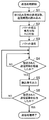
図12は、受信側の半導体装置のフローチャートである。
[ステップS11]半導体装置40の受信バッファ41は、バッファをクリアする。
[ステップS12]割り込みマスク部45は、受信タイミング生成部44によって生成される受信タイミングに応じて、割り込み信号検出部42を活性化する割り込みマスク信号を出力する。すなわち、割り込みマスク部45は、割り込み信号検出部42が割り込み信号をマスクしないようにする(割り込みマスクOFF)。
FIG. 12 is a flowchart of the semiconductor device on the receiving side.
[Step S11] The reception buffer 41 of the semiconductor device 40 clears the buffer.
[Step S12] The interrupt
[ステップS13]割り込み信号検出部42は、割り込みマスク部45からの割り込みマスクOFFの割り込みマスク信号によって、割り込み信号の受信待ちとなる。データ処理部46は、割り込み信号受信待ちのとき、受信したパケットのデータ処理以外のデータ処理を行う。
[Step S13] The interrupt
[ステップS14]パケット受信判断部43は、割り込み信号検出部42によって割り込み信号が検出されると、受信バッファ41にFLGが受信されているか否か判断する。パケット受信判断部43は、受信バッファ41にFLGが受信されていなければ、ステップS13へ進む。パケット受信判断部43は、受信バッファ41にFLGが受信されていれば、ステップS15へ進む。
[Step S14] When the interrupt
[ステップS15]割り込みマスク部45は、割り込み信号検出部42を不活性化する割り込みマスク信号を出力する。すなわち、割り込みマスク部45は、割り込み信号検出部42が割り込み信号をマスクするようにする(割り込みマスクON)。
[Step S15] The interrupt
[ステップS16]データ処理部46は、受信されたパケットのデータ処理を行う。なお、データ処理部46は、無効を示すイネーブル情報を含むパケットが受信された場合、受信されたパケットのデータは無効であると判断し、受信データのデータ処理を行わない。
[Step S16] The
このように、パケットの送信側の半導体装置は、パケットを送信したことを示す割り込み信号を所定回数、受信側の半導体装置に送信する。パケットの受信側の半導体装置は、パケットを受信したと判断した場合、その後に送信される割り込み信号を検出しないようにする。これにより、受信側の半導体装置は、パケット転送によるデータ処理の遅延を防止することができる。 As described above, the semiconductor device on the packet transmission side transmits an interrupt signal indicating that the packet has been transmitted to the semiconductor device on the reception side a predetermined number of times. When the semiconductor device on the packet receiving side determines that the packet has been received, it does not detect an interrupt signal transmitted thereafter. Thereby, the receiving-side semiconductor device can prevent a delay in data processing due to packet transfer.
なお、上記では、半導体装置の送信部分と受信部分とを別々に示したが、1つの半導体装置が送信部分と受信部分を有していてもよい。例えば、半導体装置は、図6で示したブロックと図8で示したブロックを有していてもよい。 In the above description, the transmission part and the reception part of the semiconductor device are shown separately, but one semiconductor device may have the transmission part and the reception part. For example, the semiconductor device may include the block illustrated in FIG. 6 and the block illustrated in FIG.
1,2 半導体装置
1a 送信部
1b 送信信号送信部
2a 受信部
2b 送信信号検出部
2c パケット受信判断部
2d 送信信号マスク部
DESCRIPTION OF
Claims (4)
第1の伝送路を通じて前記パケットを受信する受信部と、
前記パケットを送信した送信側半導体装置から前記第1の伝送路とは異なる第2の伝送路を通じて当該パケットの送信完了後に複数回送信される、当該パケットを送信したことを示すパケット送信信号を検出する送信信号検出部と、
前記送信信号検出部による前記パケット送信信号の検出に応じて、前記受信部による前記パケットの受信が完了しているか否か判断するパケット受信判断部と、
前記パケット受信判断部によって前記パケットの受信が完了していると判断された場合、前記送信信号検出部がその後に送信される前記パケット送信信号を検出しないようにする送信信号マスク部と、
を有することを特徴とする半導体装置。 In a semiconductor device that receives a packet,
A receiving unit that receives the packet through a first transmission path ;
A packet transmission signal indicating that the packet has been transmitted is detected a plurality of times after the transmission of the packet is completed through a second transmission path different from the first transmission path from the transmitting semiconductor device that has transmitted the packet. A transmission signal detector that performs
And the transmission signal in response to detection of the packet transmission signal by the detecting unit, the packet reception determination unit that determines whether the reception of the packet by the receiving unit is completed,
A transmission signal mask unit that prevents the transmission signal detection unit from detecting the packet transmission signal transmitted thereafter, when the packet reception determination unit determines that the reception of the packet is completed ;
A semiconductor device comprising:
前記送信信号マスク部は、前記受信タイミングに基づいて前記送信信号検出部が前記パケット送信信号を検出するようにすることを特徴とする請求項1または2記載の半導体装置。 A timing generation unit that generates a reception timing synchronized with a transmission completion timing of the packet of the transmission-side semiconductor device;
The semiconductor device according to claim 1, wherein the transmission signal mask unit causes the transmission signal detection unit to detect the packet transmission signal based on the reception timing.
第1の伝送路を通じて前記パケットを受信部によって受信し、
前記パケットを送信した送信側半導体装置から前記第1の伝送路とは異なる第2の伝送路を通じて当該パケットの送信完了後に複数回送信される、当該パケットを送信したことを示すパケット送信信号を検出し、
前記パケット送信信号の検出に応じて、前記受信部による前記パケットの受信が完了しているか否か判断し、
前記パケットの受信が完了していると判断した場合、その後に送信される前記パケット送信信号を検出しないようにする、
ことを特徴とするパケット受信方法。
In a packet receiving method of a semiconductor device that receives a packet,
Receiving the packet through the first transmission path by the receiving unit;
A packet transmission signal indicating that the packet has been transmitted is detected a plurality of times after the transmission of the packet is completed through a second transmission path different from the first transmission path from the transmitting semiconductor device that has transmitted the packet. And
In response to detection of the packet transmission signal, it is determined whether or not reception of the packet by the receiving unit is completed,
When determined that the receiving of the packet is complete, so as not to detect the packet transmission signal to be transmitted subsequently,
And a packet receiving method.
Priority Applications (1)
| Application Number | Priority Date | Filing Date | Title |
|---|---|---|---|
| JP2010147974A JP5569185B2 (en) | 2010-06-29 | 2010-06-29 | Semiconductor device and packet receiving method |
Applications Claiming Priority (1)
| Application Number | Priority Date | Filing Date | Title |
|---|---|---|---|
| JP2010147974A JP5569185B2 (en) | 2010-06-29 | 2010-06-29 | Semiconductor device and packet receiving method |
Publications (2)
| Publication Number | Publication Date |
|---|---|
| JP2012015630A JP2012015630A (en) | 2012-01-19 |
| JP5569185B2 true JP5569185B2 (en) | 2014-08-13 |
Family
ID=45601582
Family Applications (1)
| Application Number | Title | Priority Date | Filing Date |
|---|---|---|---|
| JP2010147974A Expired - Fee Related JP5569185B2 (en) | 2010-06-29 | 2010-06-29 | Semiconductor device and packet receiving method |
Country Status (1)
| Country | Link |
|---|---|
| JP (1) | JP5569185B2 (en) |
Family Cites Families (8)
| Publication number | Priority date | Publication date | Assignee | Title |
|---|---|---|---|---|
| JPS615645A (en) * | 1984-06-20 | 1986-01-11 | Toshiba Corp | Data transmission method |
| JP2000332855A (en) * | 1999-05-17 | 2000-11-30 | Nec Eng Ltd | Communication processing unit and data transfer processing method |
| JP2001197144A (en) * | 2000-01-14 | 2001-07-19 | Fuji Electric Co Ltd | transceiver |
| EP1667395A4 (en) * | 2003-09-18 | 2010-05-26 | Nomura Res Inst Co Ltd | COMMUNICATION SYSTEM AND DEVICE AND DATA RETRANSMISSION CONTROL METHOD |
| JP4075898B2 (en) * | 2005-03-23 | 2008-04-16 | セイコーエプソン株式会社 | Data transfer control device and electronic device |
| JP4361540B2 (en) * | 2006-03-06 | 2009-11-11 | 富士通テン株式会社 | Gateway device, data transfer method, and program |
| WO2009141992A1 (en) * | 2008-05-19 | 2009-11-26 | パナソニック株式会社 | Communication processor, communication processing method, control method and communication device of communication processor |
| JP2010050699A (en) * | 2008-08-21 | 2010-03-04 | Kawasaki Microelectronics Inc | Network equipment device |
-
2010
- 2010-06-29 JP JP2010147974A patent/JP5569185B2/en not_active Expired - Fee Related
Also Published As
| Publication number | Publication date |
|---|---|
| JP2012015630A (en) | 2012-01-19 |
Similar Documents
| Publication | Publication Date | Title |
|---|---|---|
| JP2006503479A5 (en) | ||
| JP2010056947A (en) | Transit time fixing apparatus | |
| CN106464412B (en) | Sending method, equipment, processing method and the optical switching device of light packet | |
| CN1276635C (en) | Priority enhanced information transfer device and its method | |
| US20050066255A1 (en) | Status report missing detection in a communication system | |
| CN112771827A (en) | Wirelessly transmitting and receiving packets | |
| JP5569185B2 (en) | Semiconductor device and packet receiving method | |
| WO2010139216A1 (en) | Method and system for realizing transmission of message between an extended processor and a switch chip | |
| EP2442502A1 (en) | Serial transmission apparatus, information processing apparatus, and serial transmission method | |
| MXPA03011468A (en) | Communication apparatus and method for supporting carrier sense multiple access/collision detection. | |
| JP2002158613A (en) | Provider connection device and mobile communication system | |
| EP1991012B1 (en) | Base station and handover control method | |
| EP2916523B1 (en) | Data stream and data packet transmission method and device | |
| US20110267974A1 (en) | Communication apparatus, communication system, and slave station apparatus | |
| JP6146409B2 (en) | Communication apparatus and communication method | |
| JP4254048B2 (en) | Transmission system of digital protection relay system | |
| WO2018058538A1 (en) | Information transmission method, network device and terminal device | |
| JP4897393B2 (en) | Data transmission device | |
| JP5536590B2 (en) | Wireless communication system | |
| CN102833749B (en) | Wireless communication method and system | |
| JP2008199432A (en) | Data transfer device and health check data processing method | |
| EP1525722A2 (en) | Packet signal processing architecture | |
| WO2004032437A3 (en) | Method and apparatus for processing superframes using an arbitration system | |
| JP2010050699A (en) | Network equipment device | |
| JP4273159B2 (en) | Network device and congestion detection method |
Legal Events
| Date | Code | Title | Description |
|---|---|---|---|
| A621 | Written request for application examination |
Free format text: JAPANESE INTERMEDIATE CODE: A621 Effective date: 20130507 |
|
| A977 | Report on retrieval |
Free format text: JAPANESE INTERMEDIATE CODE: A971007 Effective date: 20140227 |
|
| A131 | Notification of reasons for refusal |
Free format text: JAPANESE INTERMEDIATE CODE: A131 Effective date: 20140311 |
|
| A521 | Written amendment |
Free format text: JAPANESE INTERMEDIATE CODE: A523 Effective date: 20140502 |
|
| TRDD | Decision of grant or rejection written | ||
| A01 | Written decision to grant a patent or to grant a registration (utility model) |
Free format text: JAPANESE INTERMEDIATE CODE: A01 Effective date: 20140527 |
|
| A61 | First payment of annual fees (during grant procedure) |
Free format text: JAPANESE INTERMEDIATE CODE: A61 Effective date: 20140609 |
|
| R150 | Certificate of patent or registration of utility model |
Ref document number: 5569185 Country of ref document: JP Free format text: JAPANESE INTERMEDIATE CODE: R150 |
|
| LAPS | Cancellation because of no payment of annual fees |