JP5563020B2 - Liquid crystal display - Google Patents
Liquid crystal display Download PDFInfo
- Publication number
- JP5563020B2 JP5563020B2 JP2012134289A JP2012134289A JP5563020B2 JP 5563020 B2 JP5563020 B2 JP 5563020B2 JP 2012134289 A JP2012134289 A JP 2012134289A JP 2012134289 A JP2012134289 A JP 2012134289A JP 5563020 B2 JP5563020 B2 JP 5563020B2
- Authority
- JP
- Japan
- Prior art keywords
- color filter
- spacer
- pixel
- liquid crystal
- crystal display
- Prior art date
- Legal status (The legal status is an assumption and is not a legal conclusion. Google has not performed a legal analysis and makes no representation as to the accuracy of the status listed.)
- Active
Links
- 239000004973 liquid crystal related substance Substances 0.000 title claims description 101
- 125000006850 spacer group Chemical group 0.000 claims description 211
- 239000000758 substrate Substances 0.000 claims description 154
- 239000010408 film Substances 0.000 description 37
- 239000011159 matrix material Substances 0.000 description 31
- 230000002093 peripheral effect Effects 0.000 description 29
- 239000010410 layer Substances 0.000 description 25
- 238000000034 method Methods 0.000 description 23
- 239000000463 material Substances 0.000 description 9
- 239000011324 bead Substances 0.000 description 8
- 230000000694 effects Effects 0.000 description 8
- 238000010586 diagram Methods 0.000 description 6
- NJPPVKZQTLUDBO-UHFFFAOYSA-N novaluron Chemical compound C1=C(Cl)C(OC(F)(F)C(OC(F)(F)F)F)=CC=C1NC(=O)NC(=O)C1=C(F)C=CC=C1F NJPPVKZQTLUDBO-UHFFFAOYSA-N 0.000 description 6
- 230000035882 stress Effects 0.000 description 6
- 229910021417 amorphous silicon Inorganic materials 0.000 description 5
- 238000002161 passivation Methods 0.000 description 4
- 230000015572 biosynthetic process Effects 0.000 description 3
- 239000003086 colorant Substances 0.000 description 3
- 238000010030 laminating Methods 0.000 description 3
- 238000000206 photolithography Methods 0.000 description 3
- 238000007789 sealing Methods 0.000 description 3
- 238000005530 etching Methods 0.000 description 2
- 239000011521 glass Substances 0.000 description 2
- 238000004519 manufacturing process Methods 0.000 description 2
- 239000011347 resin Substances 0.000 description 2
- 229920005989 resin Polymers 0.000 description 2
- NIXOWILDQLNWCW-UHFFFAOYSA-N acrylic acid group Chemical group C(C=C)(=O)O NIXOWILDQLNWCW-UHFFFAOYSA-N 0.000 description 1
- 239000010953 base metal Substances 0.000 description 1
- 230000005540 biological transmission Effects 0.000 description 1
- 230000008602 contraction Effects 0.000 description 1
- 230000003247 decreasing effect Effects 0.000 description 1
- 230000002950 deficient Effects 0.000 description 1
- 230000005684 electric field Effects 0.000 description 1
- 239000000945 filler Substances 0.000 description 1
- 238000003475 lamination Methods 0.000 description 1
- 239000007788 liquid Substances 0.000 description 1
- 239000011344 liquid material Substances 0.000 description 1
- 239000002184 metal Substances 0.000 description 1
- 239000000049 pigment Substances 0.000 description 1
- 239000011241 protective layer Substances 0.000 description 1
- 239000007787 solid Substances 0.000 description 1
- 239000011343 solid material Substances 0.000 description 1
- 230000000087 stabilizing effect Effects 0.000 description 1
- 230000008646 thermal stress Effects 0.000 description 1
- 239000010409 thin film Substances 0.000 description 1
- 239000002023 wood Substances 0.000 description 1
Images


Landscapes
- Liquid Crystal (AREA)
Description
本発明は液晶表示装置において、支柱方式によってTFT基板と対向基板の間隔を規定する技術に関する。 The present invention relates to a technique for defining a distance between a TFT substrate and a counter substrate by a column system in a liquid crystal display device.
液晶表示装置では画素電極や薄膜トランジスタ(TFT)が形成されたTFT基板とカラーフィルタ等が形成された対向基板との間に液晶を充填し、この液晶の分子を電界によって制御することによって画像を形成する。TFT基板と対向基板の間の間隔は数ミクロンと非常に小さい。TFT基板と対向基板の間の間隔を適切に設定することは、液晶による光の透過を制御するためには極めて重要である。 In a liquid crystal display device, liquid crystal is filled between a TFT substrate on which pixel electrodes and thin film transistors (TFTs) are formed and a counter substrate on which color filters are formed, and an image is formed by controlling the molecules of the liquid crystal by an electric field. To do. The distance between the TFT substrate and the counter substrate is as small as several microns. It is extremely important to appropriately set the distance between the TFT substrate and the counter substrate in order to control light transmission by the liquid crystal.
TFT基板と対向基板の間隔は、従来は、ビーズ等を分散することによって行われてきた。しかし、ビーズを分散させると、画素電極が形成された領域にまで、ビーズが分散されることになり、この部分において光が散乱されてコントラストが低下するという問題があった。 Conventionally, the interval between the TFT substrate and the counter substrate has been performed by dispersing beads or the like. However, when the beads are dispersed, the beads are dispersed to the region where the pixel electrode is formed, and there is a problem that light is scattered in this portion and the contrast is lowered.
一方、従来の液晶の充填方法は、TFT基板と対向基板との間をシールし、シールの一部に開口を設け、そこから液晶を注入する方法、およびTFT基板上に液晶を必要量滴下し、その後対向基板をシールして液晶を封止する方法などが開発されている。何れの場合においても、ビーズを分散させる場合は、液晶を滴下する際に、ビーズが移動し、ビーズの多い場所と少ない場所が生ずる。また、ビーズはバックライトの光が透過する画素領域内にも分散され、開口率が低下し、開口率低下の原因となり得る。 On the other hand, the conventional liquid crystal filling method is to seal between the TFT substrate and the counter substrate, provide an opening in a part of the seal, and inject liquid crystal from there, and drop the required amount of liquid crystal on the TFT substrate. Thereafter, a method of sealing the counter substrate and sealing the liquid crystal has been developed. In either case, when the beads are dispersed, when the liquid crystal is dropped, the beads move, and a place with many beads and a place with few beads are generated. Further, the beads are dispersed also in the pixel region through which the light of the backlight is transmitted, and the aperture ratio is lowered, which can cause the aperture ratio to be lowered.
以上のような問題を解決するために、TFT基板と対向基板との間隔を規定する方法として、対向基板上に有機膜による支柱を形成する方法(支柱方式)が開発されている。支柱は、画素電極が存在していない部分すなわち、バックライト等が透過しない部分に設置することが出来る。したがって、輝度(開口率)を低下させることはない。また、支柱は対向基板に固定されているために、液晶を滴下した場合も移動することは無い。したがって、支柱によって間隔を維持する方法は液晶を滴下する方式(液晶滴下封入方式)にも好適である。 In order to solve the above problems, as a method for defining the distance between the TFT substrate and the counter substrate, a method (column system) in which a column made of an organic film is formed on the counter substrate has been developed. The support column can be installed in a portion where the pixel electrode is not present, that is, a portion where the backlight or the like is not transmitted. Therefore, the luminance (aperture ratio) is not reduced. In addition, since the column is fixed to the counter substrate, the column does not move even when the liquid crystal is dropped. Therefore, the method of maintaining the interval by the support is also suitable for a method of dropping liquid crystal (liquid crystal dropping and sealing method).
この支柱は一般的には、対向基板のブラックマトリクス上に形成されている。支柱はアクリル等の樹脂によって形成されるが、従来は、この支柱を形成するために、フォトリソグラフィ工程を1回必要としていた。支柱のためのフォトリソグラフィ工程を無くすために、支柱をカラーフィルタを積層することによって形成する技術が「特許文献1」に記載されている。
This support column is generally formed on a black matrix of a counter substrate. The support is formed of a resin such as acrylic, but conventionally, a photolithography process has been required once to form the support. In order to eliminate the photolithography process for the support, a technique for forming the support by stacking color filters is described in “
一方、カラーフィルタを積層して支柱を形成する場合、支柱部分においては、各色のカラーフィルタの位置を正確に合わせないと支柱の高さがばらついてしまうことになる。この問題点を対策するために、支柱として使用する各カラーフィルタの平面形状を長方形とし、積層するカラーフィルタ毎に、平面形状の長方形の長軸の向きを90度変えることによって、支柱の高さを一定に保つ技術が「特許文献2」に記載されている。
On the other hand, in the case where the column is formed by stacking color filters, the column height varies in the column portion unless the position of the color filter of each color is accurately aligned. In order to prevent this problem, the planar shape of each color filter used as a support column is rectangular, and the length of the support column is changed by changing the major axis of the rectangular shape of the planar shape by 90 degrees for each color filter to be stacked. A technique for maintaining a constant value is described in “
TFT基板と対向基板の間隔は、駆動方式、液晶材料等によって最適な値が存在し、この値は製品毎に異なる、TFT基板と対向基板間隔が適正でないとコントラストが低下する。従来のカラーフィルタを積層することでスペーサを形成する場合は、スペーサの高さは、カラーフィルタの厚さの倍数に固定され、TFT基板と対向基板の間隔を最適な値に設定することが難しかった。 There is an optimum value for the distance between the TFT substrate and the counter substrate depending on the driving method, the liquid crystal material, and the like, and this value varies depending on the product. When forming a spacer by stacking conventional color filters, the height of the spacer is fixed to a multiple of the thickness of the color filter, and it is difficult to set the distance between the TFT substrate and the counter substrate to an optimum value. It was.
また、表示装置では、画像を形成する表示領域の周辺の対向基板に、額縁状に、遮光膜であるブラックマトリクスが形成される。周辺のブラックマトリクスの部分に対応するTFT基板には、表示領域程には配線等が存在していないために、周辺部におけるスペーサは、表示領域におけるスペーサよりも高くしなければならない。しかし、従来技術でのカラーフィルタの積層によるスペーサでは、このように、高さの異なるスペーサを同一液晶表示パネル内に形成することは困難であった。 In the display device, a black matrix, which is a light shielding film, is formed in a frame shape on a counter substrate around a display area where an image is formed. Since the TFT substrate corresponding to the peripheral black matrix portion does not have wiring or the like in the display region, the spacer in the peripheral portion must be higher than the spacer in the display region. However, it is difficult to form spacers with different heights in the same liquid crystal display panel in the conventional spacers formed by stacking color filters.
本発明は、以上のような、問題点を解決して、カラーフィルタをスペーサとして使用しつつ、スペーサの高さを必要に応じて細かく制御することが出来る技術を実現することである。 An object of the present invention is to solve the above problems and to realize a technique capable of finely controlling the height of a spacer as required while using a color filter as a spacer.
一方、液晶表示装置における液晶材料の値段は高く、液晶表示装置のコスト低減のためには、液晶の使用量を低減する必要がある。また、液晶はスペーサ、ガラス、配線等の固形物に比べて熱膨張係数が大きい。液晶表示装置は戸外でも使用されるために、使用温度範囲が広い。したがって、液晶の熱膨張あるいは収縮によって液晶表示パネルの内部は様々なストレスを受けることになる。このような液晶による熱ストレスを緩和するには液晶の量が少ないほうが良い。 On the other hand, the price of the liquid crystal material in the liquid crystal display device is high, and it is necessary to reduce the amount of liquid crystal used in order to reduce the cost of the liquid crystal display device. Liquid crystals have a larger coefficient of thermal expansion than solid materials such as spacers, glass, and wiring. Since the liquid crystal display device is used even outdoors, the operating temperature range is wide. Accordingly, the liquid crystal display panel is subjected to various stresses due to thermal expansion or contraction of the liquid crystal. In order to relieve the thermal stress caused by such liquid crystal, it is better that the amount of liquid crystal is small.
本発明の他の課題は、液晶表示パネル内の液晶の量を低減することによって、液晶表示装置のコストの低減と、液晶表示パネルの、液晶の熱膨張によるストレスを緩和して液晶表示パネルの信頼性を向上させることである。 Another object of the present invention is to reduce the amount of liquid crystal in the liquid crystal display panel, thereby reducing the cost of the liquid crystal display device and alleviating the stress caused by the thermal expansion of the liquid crystal display panel. It is to improve reliability.
本発明は、複数のカラーフィルタを積層することによってスペーサを形成し、スペーサを構成する複数のカラーフィルタの面積を変化させることによってスペーサの高さを木目細かく制御することを特徴とする。 The present invention is characterized in that a spacer is formed by laminating a plurality of color filters, and the height of the spacer is finely controlled by changing the areas of the plurality of color filters constituting the spacer.
また、本発明は高さの異なる第1のスペーサと第2のスペーサを形成し、第1のスペーサまたは第2のスペーサを構成する複数のカラーフィルタの各面積を変化させ、または、複数のカラーフィルタの積層の順番を変化させることによって、第1のスペーサまたは第2のスペーサの高さに差を設けることを特徴とする。 In the present invention, the first spacer and the second spacer having different heights are formed, the areas of the plurality of color filters constituting the first spacer or the second spacer are changed, or the plurality of colors A difference is provided in the height of the first spacer or the second spacer by changing the stacking order of the filters.
さらに本発明は、画像形成に寄与しない画素と画素の間に、カラーフィルタを設置することによって液晶の使用量を減少させることを特徴とする。具体的な手段は次のとおりである。 Furthermore, the present invention is characterized in that the amount of liquid crystal used is reduced by installing a color filter between pixels that do not contribute to image formation. Specific means are as follows.
(1)TFT基板と、対向基板と、前記TFT基板と前記対向基板との間に液晶が挟持された液晶表示装置であって、前記対向基板には、第1のカラーフィルタによって第1の色を表示する第1の画素と、第2のカラーフィルタによって第2の色を表示する第2の画素と、第3のカラーフィルタによって第3の色を表示する第3の画素とがマトリクス状に形成され、前記対向基板には、前記TFT基板との間隔を規定する第1のスペーサと、前記第1のスペーサよりも高さが低い第2のスペーサが形成され、前記第1のスペーサは複数のカラーフィルタを積層することによって形成され、前記複数のカラーフィルタのうちの下側のカラーフィルタの面積は、前記上側のカラーフィルタの面積よりも大きく、前記第2のスペーサは、複数のカラーフィルタの積層によって形成され、前記複数のカラーフィルタのうちの下側のカラーフィルタの面積は、前記上側のカラーフィルタの面積よりも小さいことを特徴とする液晶表示装置。 (1) A liquid crystal display device in which a liquid crystal is sandwiched between a TFT substrate, a counter substrate, and the TFT substrate and the counter substrate. The first color filter is provided on the counter substrate by a first color filter. A first pixel that displays the second color, a second pixel that displays the second color using the second color filter, and a third pixel that displays the third color using the third color filter are arranged in a matrix. The counter substrate is formed with a first spacer for defining a distance from the TFT substrate and a second spacer having a height lower than that of the first spacer, and the first spacer includes a plurality of first spacers. Of the plurality of color filters, the area of the lower color filter is larger than the area of the upper color filter, and the second spacer has a plurality of color filters. Formed by lamination of the filter, the area of the lower color filter among the plurality of color filters, liquid crystal display device, characterized in that less than the area of the upper color filter.
(2)前記第1のスペーサは、3層のカラーフィルタによって形成され、最上層のカラーフィルタの面積が最も小さく、前記第2のスペーサは3層のカラーフィルタによって形成され、最下層のカラーフィルタの面積が最も小さいことを特徴とする(1)に記載の液晶表示装置。 (2) The first spacer is formed by a three-layer color filter, and the area of the uppermost color filter is the smallest, and the second spacer is formed by a three-layer color filter, and the lowermost color filter. The liquid crystal display device according to (1), wherein the area of the liquid crystal display device is the smallest.
(3)前記第2のスペーサは3層のカラーフィルタによって形成され、最下層の層のカラーフィルタが最も面積が小さく、最上層の層のカラーフィルタの面積が最も大きく、中間の層のカラーフィルタの面積は、最下層のカラーフィルタの面積よりも大きく、最上層のカラーフィルタの面積よりも小さいことを特徴とする(1)に記載の液晶表示装置。 (3) The second spacer is formed by three layers of color filters, the color filter of the lowermost layer has the smallest area, the area of the color filter of the uppermost layer is the largest, and the color filter of the intermediate layer The liquid crystal display device according to (1), wherein the area is larger than the area of the lowermost color filter and smaller than the area of the uppermost color filter.
(4)前記第1のスペーサは、縦方向に配列した前記第1の画素の間に形成され、前記第2のスペーサは、縦方向に配列した前記第2の画素の間に形成されていることを特徴とする(1)に記載の液晶表示装置。 (4) The first spacer is formed between the first pixels arranged in the vertical direction, and the second spacer is formed between the second pixels arranged in the vertical direction. (1) The liquid crystal display device according to (1).
(5)TFT基板と、対向基板と、前記TFT基板と前記対向基板との間に液晶が挟持された液晶表示装置であって、前記対向基板には、第1のカラーフィルタによって第1の色を表示する第1の画素が縦方向に配列し、第2のカラーフィルタによって第2の色を表示する第2の画素が縦方向に配列し、第3のカラーフィルタによって第3の色を表示する第3の画素が縦方向に配列し、前記第1のカラーフィルタは前記第1の画素を覆って縦方向にストライプ状に延在し、前記第2のカラーフィルタは前記第2の画素を覆って縦方向にストライプ状に延在し、前記第3のカラーフィルタは前記第3の画素を覆って縦方向に延在し、前記第1の画素と前記第1の画素の間には、前記第1のカラーフィルタを含む複数のカラーフィルタが積層された第1のスペーサが形成されていることを特徴とする液晶表示装置。 (5) A liquid crystal display device in which liquid crystal is sandwiched between a TFT substrate, a counter substrate, and the TFT substrate and the counter substrate, wherein the first color filter is provided on the counter substrate by a first color filter. Are arranged in the vertical direction, the second color filter is used to display the second color, and the third color filter is used to display the third color. Third pixels arranged in the vertical direction, the first color filter extends in a stripe shape in a vertical direction covering the first pixel, and the second color filter includes the second pixel. The third color filter extends in the vertical direction so as to cover the third pixel, and extends between the first pixel and the first pixel. A plurality of color filters including the first color filter are stacked. The liquid crystal display device, wherein a first spacer is formed.
(6)前記第2の画素と前記第2の画素の間には前記第2のカラーフィルタを含む複数のカラーフィルタによって第2のスペーサが形成され、前記第1のスペーサの高さは、前記第2のスペーサの高さよりも大きいことを特徴とする(5)に記載の液晶表示装置。 (6) A second spacer is formed between the second pixel and the second pixel by a plurality of color filters including the second color filter, and the height of the first spacer is The liquid crystal display device according to (5), which is larger than a height of the second spacer.
(7)前記第1のカラーフィルタは、前記第2の画素と前記第2の画素の間と前記第3の画素と前記第3の画素の間をストライプ状に横方向に延在していることを特徴とする(5)に記載の液晶表示装置。 (7) The first color filter extends in a horizontal direction in a stripe shape between the second pixel and the second pixel, and between the third pixel and the third pixel. (5) The liquid crystal display device according to (5).
(8)前記第1のスペーサは前記第1のカラーフィルタを含む3層のカラーフィルタによって形成され、前記第2のスペーサは前記第2のカラーフィルタを含む3層のカラーフィルタによって形成されていることを特徴とする(7)に記載の液晶表示装置。 (8) The first spacer is formed by a three-layer color filter including the first color filter, and the second spacer is formed by a three-layer color filter including the second color filter. (7) The liquid crystal display device as described above.
(9)前記第3の画素と前記第3の画素の間には、複数のカラーフィルタが積層されていることを特徴とする(8)に記載の液晶表示装置。 (9) The liquid crystal display device according to (8), wherein a plurality of color filters are stacked between the third pixel and the third pixel.
(10)TFT基板と、対向基板と、前記TFT基板と前記対向基板との間に液晶が挟持された液晶表示装置であって、前記対向基板には、画像を表示する表示領域と、前記表示領域を囲んで額縁状の遮光領域が形成されており、前記対向基板の前記表示領域には、第1のカラーフィルタによって第1の色を表示する第1の画素と、第2のカラーフィルタによって第2の色を表示する第2の画素と、第3のカラーフィルタによって第3の色を表示する第3の画素とがマトリクス状に形成され、前記対向基板の前記額縁状の遮光領域には、前記第1のカラーフィルタ、前記第2のカラーフィルタ、または、前記第3のカラーフィルタによって前記対向基板と前記TFT基板の間隔を規定するスペーサ形成されており、前記スペーサの高さは、前記遮光領域の外側程高さが高いことを特徴とする液晶表示装置。 (10) A liquid crystal display device in which liquid crystal is sandwiched between a TFT substrate, a counter substrate, and the TFT substrate and the counter substrate, wherein the counter substrate has a display area for displaying an image and the display A frame-shaped light-shielding region is formed surrounding the region, and the display region of the counter substrate includes a first pixel that displays a first color by a first color filter and a second color filter. A second pixel for displaying the second color and a third pixel for displaying the third color by the third color filter are formed in a matrix, and the frame-shaped light shielding region of the counter substrate has The first color filter, the second color filter, or the third color filter is used to form a spacer that defines a distance between the counter substrate and the TFT substrate. A liquid crystal display device comprising a higher outer as the height of the light shielding region.
(11)前記スペーサを構成する前記第1のカラーフィルタ、前記第2のカラーフィルタ、または、前記第3のカラーフィルタのうちのいずれかは、前記遮光領域の外側程面積が大きいことを特徴とする(10)に記載の液晶表示装置。 (11) One of the first color filter, the second color filter, and the third color filter constituting the spacer has a larger area toward the outer side of the light shielding region. The liquid crystal display device according to (10).
(12)前記スペーサは、前記第1のカラーフィルタ、前記第2のカラーフィルタ、または、前記第3のカラーフィルタのうちの複数によって形成されていることを特徴とする(11)に記載の液晶表示装置。 (12) The liquid crystal according to (11), wherein the spacer is formed of a plurality of the first color filter, the second color filter, or the third color filter. Display device.
本発明は、複数のカラーフィルタを積層することによってスペーサを形成するので、スペーサを形成するためのフォトプロセスを別途必要とせず、また、スペーサを構成する複数のカラーフィルタの面積を変化させるのでスペーサの高さを木目細かく制御することが出来る。 In the present invention, since the spacer is formed by laminating a plurality of color filters, a photo process for forming the spacer is not required separately, and the area of the plurality of color filters constituting the spacer is changed. It is possible to finely control the height of the wood.
また、本発明は高さの異なる第1のスペーサと第2のスペーサを形成するにあたり、第1のスペーサまたは第2のスペーサを構成する複数のカラーフィルタの各面積を変化させ、または、複数のカラーフィルタの積層の順番を変化させることによって、第1のスペーサまたは第2のスペーサの高さに差を設けるので、第1のスペーサおよび第2のスペーサの高さを木目細かく制御することが出来る。 In the present invention, when forming the first spacer and the second spacer having different heights, the areas of the plurality of color filters constituting the first spacer or the second spacer are changed, or a plurality of By changing the stacking order of the color filters, a difference is provided in the height of the first spacer or the second spacer, so that the height of the first spacer and the second spacer can be finely controlled. .
さらに本発明は、画像形成に寄与しない画素と画素の間に、カラーフィルタを設置するので、液晶の使用量を減少させることが出来、液晶表示装置の材料費を低減することが出来る。 Furthermore, according to the present invention, since a color filter is provided between pixels that do not contribute to image formation, the amount of liquid crystal used can be reduced, and the material cost of the liquid crystal display device can be reduced.
図面を用いて、本発明の詳細な内容を開示する。図6は、本発明が適用される液晶表示装置に使用される液晶表示パネルの平面図である。図6において、TFT基板100と対向基板200が積層されている。TFT基板100と対向基板200は、周辺に形成されたシール部150によって接着しており、シール部150の内部に液晶が封入されている。TFT基板100と対向基板200との間隔はスペーサによって維持されている。なお、本明細書におけるスペーサは、対向基板に形成された支柱であるが、以後この支柱を単にスペーサと呼ぶ。
The detailed contents of the present invention will be disclosed with reference to the drawings. FIG. 6 is a plan view of a liquid crystal display panel used in a liquid crystal display device to which the present invention is applied. In FIG. 6, a
TFT基板100は、対向基板200より大きく形成されており、図6の左側および下側のTFT基板100の周辺には、外部から液晶表示パネルに映像信号、電源等を供給するための端子部130が形成されている。対向基板200の大部分には表示領域210が形成されている。表示領域210の周辺にはブラックマトリクスBMによる周辺遮光膜220が額縁状に形成されている。
The
図7は、対向基板200の表示領域210における画素の配置を示す例である。図7において、横方向には、赤画素RP、青画素BP、緑画素GPが一定ピッチPxで配置されている。なお赤画素RP、青画素BP、緑画素GP等は、正確には赤画素RP、青画素BP、緑画素GPに対応するBMのホールであるが、複雑な呼称を避けるために、単に、赤画素RP、青画素BP、緑画素GPと呼ぶ。縦方向には同じ色の画素が一定ピッチPyで配置されている。各画素の幅はPwで、各画素の縦径はPhである。横方向のピッチPxは、例えば170.25μm、縦方向のピッチPyは例えば、510.75μmである。一方、画素の幅Pwは143.25μm、画素の縦径Phは410.75μmである。
FIG. 7 is an example showing the arrangement of pixels in the
スペーサは図7に示すように、縦方向の画素間のブラックマトリクスBM上に形成されるので、スペーサの形成のために利用できる領域は、縦方向は100μmである。スペーサが横方向に利用できる幅は特に制約は無い。図7において、スペーサの平面は円形であるが、スペーサの面積を大きくしたい場合は、スペーサの平面形状を楕円形状あるいは、長方形状としても良い。図7においては、スペーサの平面形状のみ記載している。スペーサの縦方向の断面形状は厳密には台形となるが、台形の上部と下部とでは、面積に大きな差は無い。図7に示すスペーサの平面図は、スペーサの上部形状と考えてよい。 As shown in FIG. 7, since the spacer is formed on the black matrix BM between the pixels in the vertical direction, the area that can be used for forming the spacer is 100 μm in the vertical direction. The width that the spacer can be used in the lateral direction is not particularly limited. In FIG. 7, the plane of the spacer is circular. However, when it is desired to increase the area of the spacer, the planar shape of the spacer may be elliptical or rectangular. In FIG. 7, only the planar shape of the spacer is shown. Strictly speaking, the vertical cross-sectional shape of the spacer is a trapezoid, but there is no significant difference in area between the upper and lower portions of the trapezoid. The plan view of the spacer shown in FIG. 7 may be considered as the upper shape of the spacer.
図7において、緑画素GPと緑画素GPの間には第1スペーサ10が、青画素BPと青画素BPの間には第2スペーサ20が形成されているが、赤画素RPと赤画素RPの間にはスペーサは形成されていない。また、第1スペーサ10のほうが第2スペーサ20よりも高さが高い。通常は、第1スペーサ10によってTFT基板100と対向基板200の間隔が規定されている。外部から液晶表示パネルに圧力が加わった場合、第1スペーサ10間のTFT基板100と対向基板200の間隔が小さくなるが、このときに、第2スペーサ20はTFT基板100と接触することによって、TFT基板100あるいは対向基板200の過度の変形を防止する。
In FIG. 7, a
図8はTFT基板100において、対向基板200に形成されたスペーサが接触する部分を示す概略図である。図8において、横方向には走査線101が延在している。走査線101が存在する部分は、図7において、縦方向の画素と画素の間で横方向に延在するブラックマトリクスBMに対応している。図8において、映像信号線1021が縦方向に延在し、横方向に配列されている。映像信号線1021が形成されている部分は、図7における横方向の画素と画素の間で縦方向に延在するブラックマトリクスBMに対応している。走査線101および映像信号線1021によって区切られた部分に画素電極が形成されている。画素電極の配置位置は、図7における赤画素RP、青画素BP、緑画素GP等に対応している。
FIG. 8 is a schematic view showing a portion of the
図8において、走査線101上には、第1TFT110と第2TFT120が形成されている。TFTが走査線101上に形成されているのは、走査線101をTFTのゲート電極として利用するためである。映像信号線1021はTFTのソース/ドレイン電極として使用される。図8において、TFTが2個存在している。通常は第1TFT110を使用するが、製造過程において、第1TFT110が不良になった場合に、第2TFT120を使用するように、配線を修正する。なお、第2TFT120は形成しない場合もある。図8に形成されたスルーホール130は、画素電極とTFTを接続するためのものである。図8では、TFT等の位置を示すための平面図であり、詳細配線等は省略されている。
In FIG. 8, a
図8において、第1TFT110と第2TFT120の間には、対向基板200に形成された第1スペーサ10と対応する位置に、スペーサ台座15が形成されている。TFT基板100と対向基板200を重ね合わせると、TFT基板100に形成されたスペーサ台座15が対向基板200に形成された第1スペーサ10と接触してTFT基板100と対向基板200の適正な間隔が規定される。
In FIG. 8, a
図9は、TFT基板100と対向基板200とを重ね合わせた場合の、スペーサ付近の断面図である。この断面は、例えば、図8のA−A断面に対応する部分である。図9において、対向基板200には、ブラックマトリクスBMが形成され、その上に赤カラーフィルタR、さらに緑カラーフィルタGが積層されている。緑カラーフィルタGの上には青フィルタによる柱状のスペーサが形成されている。緑カラーフィルタGあるいは青カラーフィルタB等を覆って保護層であるオーバーコート膜OCが形成されている。オーバーコート膜OCの上には、液晶を配向させるための配向膜106が形成されている。
FIG. 9 is a cross-sectional view of the vicinity of the spacer when the
TFT基板100の上には、走査線101が形成され、この走査線101はTFT部分においてはゲート電極として作用する。走査線101の上には、ゲート絶縁膜103が形成されている。TFTが形成される部分には、a−Si膜104が形成される。a−Si膜104の上部には、チャネル部を挟んでソース/ドレイン電極(SD電極102)が形成される。a−Si膜104の上にはSD電極102が3個形成されている。この場合、両脇のSD電極102をソースとすると、中央のSD電極102がドレインとなる。あるいはその逆の言い方をする場合もある。a−Si膜104のチャネル部は、TFTの特性を安定させるためのチャネルエッチングが施されている。
A
2個のTFTの間で、対向基板200に形成されたスペーサと対応する部分には、SD電極102と同じ材料、同じプロセスによって、スペーサ台座15が形成される。このスペーサ台座15には対向基板200に形成された第1スペーサ10が対応して設置される。TFTおよびスペーサ台座15を覆って、パッシベーション膜105がSiNによって形成される。パッシベーション膜105はTFTを保護するための膜である。パッシベーション膜105を覆って配向膜106が形成される。
A
図9において、対向基板200に形成された第1スペーサ10とTFT基板100に形成されたスペーサ台座15が接触している。スペーサ台座15はSD電極102と同じプロセスで形成された台座メタル1022によって形成されている。第1スペーサ10とスペーサ台座15によってTFT基板100と対向基板200の間隔が規定される。
In FIG. 9, the
第1スペーサ10に対応して、TFT基板100側にスペーサ台座15を形成することは一例であり、第1スペーサ10のみによってTFT基板100と対向基板200の間隔を規定する場合もあり得る。なお、図7に示す第2スペーサ20に対応する部分のTFT基板100には、図8に示すように、スペーサ台座15は形成されていない。
Forming the
図9において、TFT基板100と対向基板200の間に液晶が充填されている。図9に示すように、走査線101の形成された部分では、第1スペーサ10以外の場所にも、対向基板200にカラーフィルタが積層されているために、TFT基板100と対向基板200の隙間は小さい。したがって、この領域においては、液晶が充填される量は非常に少ない。
In FIG. 9, liquid crystal is filled between the
液晶によって表示を行うためには、液晶層107は一定の厚みが必要である。このように、液晶層107が一定の厚さを必要とする部分は画素電極が形成された部分である。一方、TFT基板100の走査線101が形成された領域では、液晶層107は表示に寄与しない。したがって、この部分においては、液晶層107の厚さは薄いほうが液晶の使用量を少なく出来る。液晶材料は高価であるので、この部分において、液晶の使用を少なくすることによって材料費を抑制し、液晶表示装置の製造コストを抑えることが出来る。また、液晶の量が少ないことによって、液晶の熱膨張に起因するストレスを緩和することが出来る。
In order to perform display using liquid crystal, the
図9に記載した例では、対向基板200には、対向電極は形成されていない。図9の実施例は、液晶分子1071を駆動するための画素電極と対向電極がTFT基板100上に形成されている場合である。このような構成は、液晶分子1071の向きをTFT基板100と平行な方向に回転させることによって制御するいわゆるIPS(In Plane Swithcing)方式の駆動方法において取られている。しかし、以下に述べる本発明は、IPS方式に限らず、対向基板200に対向電極が形成された一般のTN(Twisted Nematic)方式あるいは、VA(Vertical Alignment)方式等においても適用することが出来る。
In the example described in FIG. 9, the counter electrode is not formed on the
図1は本発明の第1の実施例を示す図である。図1(a)は図7の領域Aの詳細図である。図1(b)は、図1(a)のX1−X2断面図、図1(c)は、図1(a)のR1−R2断面図、図1(d)は、図1(a)のB1−B2断面図、図1(e)は、図1(a)のG1−G2断面図である。図1に示す画素電極の形は、実際の画素電極に即して凹凸が記載されている。図1において、縦方向には同一色の画素が配列しており、横方向には異なる色の画素が配列している。 FIG. 1 is a diagram showing a first embodiment of the present invention. FIG. 1A is a detailed view of region A in FIG. 1B is a cross-sectional view taken along the line X1-X2 in FIG. 1A, FIG. 1C is a cross-sectional view taken along the line R1-R2 in FIG. 1A, and FIG. B1-B2 sectional view of FIG. 1, FIG.1 (e) is G1-G2 sectional drawing of Fig.1 (a). The shape of the pixel electrode shown in FIG. 1 has irregularities in line with the actual pixel electrode. In FIG. 1, pixels of the same color are arranged in the vertical direction, and pixels of different colors are arranged in the horizontal direction.
図1(b)、図1(d)、図1(e)に示すように、緑画素GPと緑画素GPの間に第1スペーサ10が、青画素BPと青画素BPの間に第2スペーサ20が形成されている。これらのスペーサはカラーフィルタによって形成されている。図1(b)に示すように、第1スペーサ10のほうが第2スペーサ20よりも高い。
As shown in FIGS. 1B, 1D, and 1E, the
図1(b)に示すように、第1スペーサ10では、ブラックマトリクスBMの上に、赤カラーフィルタRが積層され、さらにその上に緑カラーフィルタGが積層されている。緑カラーフィルタGの上には青カラーフィルタBが柱状に積層されることでスペーサが形成されている。そしてその上にオーバーコート膜OCが形成されている。
As shown in FIG. 1B, in the
一方、図1(b)に示すように、第2スペーサ20部においては、ブラックマトリクスBM上に、先ず、柱状に赤カラーフィルタRによって形成され、その上に青カラーフィルタB、緑カラーフィルタGが積層される。そしてその上にオーバーコート膜OCが形成されている。
On the other hand, as shown in FIG. 1B, in the
第1スペーサ10が第2スペーサ20よりも高くなるのは次の理由による。第1スペーサ10も第2スペーサ20も3層のカラーフィルタが積層されて形成されることは同じである。第1スペーサ10と第2スペーサ20が異なる点は、第1スペーサ10においては、柱上のスペーサは最後に形成されるのに対し、第2スペーサ20は柱上のスペーサが最初に形成される点である。カラーフィルタは感光性の有機樹脂に顔料が分散されたものであるが、フォトリソグラフィによって加工する前は液体状である。第2スペーサ20においては、下層に柱状の赤のカラーフィルタを形成するので、その上に緑および青のカラーフィルタを積層すると、レベリング効果によって柱状形状の上のカラーフィルタが薄くなる。一方、第1スペーサ10においては、柱状形状を最後に形成するために、第2スペーサ20で生じたような、上層膜のレベリング効果は生じない。このために、第1スペーサ10のほうが第2スペーサ20よりも高さが高くなる。
The reason why the
図1(c)は、図1(a)のR1−R2断面図である。図1(c)に示すように、この部分では、ブラックマトリクスBM上には赤カラーフィルタRと緑カラーフィルタGの2層のみが積層されている。したがって、この部分の高さは、図1におけるB1−B2断面、G1−G2断面等に比して低い。 FIG.1 (c) is R1-R2 sectional drawing of Fig.1 (a). As shown in FIG. 1C, in this portion, only two layers of a red color filter R and a green color filter G are stacked on the black matrix BM. Therefore, the height of this portion is lower than the B1-B2 cross section, the G1-G2 cross section, etc. in FIG.
図1(d)は、図1(a)のB1−B2断面である。これは、第2スペーサ20の断面形状である。この部分では、ブラックマトリクスBM上に赤カラーフィルタR、緑カラーフィルタG、青カラーフィルタBの順に3層のカラーフィルタが形成されているが、赤カラーフィルタRは柱状に形成されている。したがって、レベリング効果によって赤カラーフィルタR上の緑カラーフィルタG、青カラーフィルタB等は膜厚が小さくなっていることは、前述で説明したとおりである。
FIG. 1D is a B1-B2 cross section of FIG. This is the cross-sectional shape of the
図1(e)は、図1(a)のG1−G2断面図であり、第1スペーサ10の断面形状を示している。図1(e)において、ブラックマトリクスBM上には、赤カラーフィルタR、緑カラーフィルタG、青カラーフィルタBの3層が形成されている。図1(e)においては、最後に積層される青カラーフィルタBを柱状に形成するので、赤カラーフィルタR、緑カラーフィルタG等にはレベリング効果を生じない。したがって、図1(e)に示す第1スペーサ10の方が、図1(d)に示す第2スペーサ20よりも高さが高くなる。
FIG. 1E is a G1-G2 cross-sectional view of FIG. 1A and shows a cross-sectional shape of the
図2〜図5は、図1に示す対向基板200を形成するプロセスを示す図である。図2に示すように、先ず、ブラックマトリクスBMを形成して画素を規定する。ブラックマトリクスBMは対向基板200全体に遮光膜を塗付した後、エッチングによって画素電極に対応する部分から遮光膜を除去することによって形成する。ブラックマトリクスBMの横方向に延在する帯状の部分に対応する部分には、TFT基板100において、走査線101が形成される。
2-5 is a figure which shows the process of forming the opposing board |
図3は、R画素およびブラックマトリクスBM上に赤カラーフィルタRを形成した状況を示す。赤画素RP上に赤カラーフィルタRが存在すれば、カラーフィルタ本来の役割を果たすことが出来るが、本実施例においては、赤カラーフィルタRをスペーサとして、あるいは、液晶の材料節約のために使用するので、赤画素RP以外の部分にも赤カラーフィルタRを形成している。すなわち赤カラーフィルタRを縦方向にストライプ状に形成することによって、赤画素RP間の液晶の充填量を節約する。 FIG. 3 shows a situation in which the red color filter R is formed on the R pixel and the black matrix BM. If the red color filter R exists on the red pixel RP, the original function of the color filter can be achieved. In this embodiment, the red color filter R is used as a spacer or for saving the material of the liquid crystal. For this reason, the red color filter R is also formed in portions other than the red pixel RP. That is, by forming the red color filter R in a stripe shape in the vertical direction, the liquid crystal filling amount between the red pixels RP can be saved.
また、青画素BP間の円形状の赤カラーフィルタRと、緑画素GP間の、横に長い帯状の赤カラーフィルタRは、各々、第2スペーサ20、第1スペーサ10の一部と成っている。図3において、青画素BP間の赤カラーフィルタRの平面を円形状として、緑画素GP間の赤カラーフィルタRの面積よりも小さくすることによって、青画素BP間に形成される第2スペーサ20の高さを緑画素GP間に形成される第1スペーサ10の高さよりも小さくする。
Also, a circular red color filter R between the blue pixels BP and a horizontally long strip-shaped red color filter R between the green pixels GP are part of the
次に図4に示すように、緑カラーフィルタGを形成する。図が複雑になることを避けるために図4では赤カラーフィルタRが省略されているが、緑カラーフィルタGは図3で形成された赤カラーフィルタRの上に形成される。図4において、緑カラーフィルタGは緑画素GP間を連続して縦方向にストライプ状に形成される。さらに、緑カラーフィルタGは青画素BP間、および、赤画素RP間に形成されたブラックマトリクスBMを覆うように、横方向に延在するように形成される。青画素BPと青画素BPの間は第2スペーサ20の一部となり、赤画素RPと赤画素RPの間は液晶材料を節約するための充填材となる。
Next, as shown in FIG. 4, a green color filter G is formed. Although the red color filter R is omitted in FIG. 4 to avoid the complexity of the drawing, the green color filter G is formed on the red color filter R formed in FIG. In FIG. 4, the green color filter G is formed in a stripe shape in the vertical direction continuously between the green pixels GP. Further, the green color filter G is formed to extend in the horizontal direction so as to cover the black matrix BM formed between the blue pixels BP and between the red pixels RP. A portion between the blue pixel BP and the blue pixel BP becomes a part of the
最後に図5に示すように、青カラーフィルタBを形成する。図5では、図を複雑化しないために、赤カラーフィルタRと緑カラーフィルタGが省略されているが、緑カラーフィルタGは緑カラーフィルタGの上に形成される。図5において、青画素BP間のBM上も青カラーフィルタBが覆うように、青カラーフィルタBは縦方向にストライプ状に形成されている。これによって、青画素BP間に充填されるはずの液晶材料を節約することが出来る。また、緑画素GPと緑画素GPの間には、青カラーフィルタBを円形状に形成することによって、青カラーフィルタBが第1スペーサ10の一部となる。円形状の青カラーフィルタBを最上層に形成することによって、第1スペーサ10は第2スペーサ20よりも高くすることが出来ることは、前述の説明で述べたとおりである。
Finally, as shown in FIG. 5, a blue color filter B is formed. In FIG. 5, the red color filter R and the green color filter G are omitted for the sake of simplicity, but the green color filter G is formed on the green color filter G. In FIG. 5, the blue color filter B is formed in a stripe shape in the vertical direction so that the blue color filter B covers the BM between the blue pixels BP. Thereby, the liquid crystal material that should be filled between the blue pixels BP can be saved. Further, the blue color filter B becomes a part of the
以上の例では、第1スペーサ10と第2スペーサ20の高さの差を、柱状形状のカラーフィルタの上層に形成されるカラーフィルタのレベリング効果を利用して形成した。スペーサの高さに差を持たせる方法として、上層のカラーフィルタのレベリング効果を用いる他に、カラーフィルタによって形成されるスペーサ自体の面積を変えることによって行うことも出来る。
In the above example, the difference in height between the
すなわち、カラーフィルタは液状のものを塗付してこれを感光することによって、所定の形状に形成する。この場合、カラーフィルタの面積が大きいほうが加工後の高さが大きくなる。したがって、図3あるいは、図5に示す円形状のカラーフィルタの面積を変えることによって第1スペーサ10あるいは第2スペーサ20の高さを変化させることが出来る。このように、本発明によれば、スペーサの高さを変化させるための自由度を多く持つことが出来る。
That is, the color filter is formed in a predetermined shape by applying a liquid material and exposing it to light. In this case, the height after processing becomes larger as the area of the color filter is larger. Therefore, the height of the
図10は本発明の第2の実施例を示す図である。図10(a)は、図7の領域Aの詳細図である。図10(b)は、図10(a)のX1−X2断面図、図10(c)は、図10(a)のR1−R2断面図、図10(d)は、図10(a)のB1−B2断面図、図10(e)は、図10(a)のG1−G2断面図である。図10の画素電極の形は、実際の画素電極に即して凹凸が記載されている。図10において、縦方向には同一色の画素が配列しており、横方向には異なる色の画素が配列している。 FIG. 10 is a diagram showing a second embodiment of the present invention. FIG. 10A is a detailed view of region A in FIG. 10B is a cross-sectional view taken along the line X1-X2 of FIG. 10A, FIG. 10C is a cross-sectional view taken along the line R1-R2 of FIG. 10A, and FIG. B1-B2 sectional view of FIG. 10, FIG.10 (e) is G1-G2 sectional drawing of Fig.10 (a). The shape of the pixel electrode in FIG. 10 has irregularities in line with the actual pixel electrode. In FIG. 10, pixels of the same color are arranged in the vertical direction, and pixels of different colors are arranged in the horizontal direction.
図10(b)、図10(d)、図10(e)に示すように、緑画素GPと緑画素GPの間に第1スペーサ10が、青画素BPと青画素BPの間に第2スペーサ20が形成されている。これらのスペーサはカラーフィルタによって形成されている。図1(b)に示すように、第1スペーサ10のほうが第2スペーサ20よりも高い。
As shown in FIGS. 10B, 10D, and 10E, the
本実施例が実施例1と異なる点は、第2スペーサ20の高さと第1スペーサ10の高さとの差を、実施例1におけるよりも大きくしたことである。これは、第2スペーサ20を実施例1とは異なる方法で形成し、第2スペーサ20の高さをより小さくしていることによる。図10において、緑画素GP間に形成されている第1スペーサ10の形状と構成は実施例1と同様である。これに対して本実施例では、図10(a)に示すように、青画素BP間の第2スペーサ20は、平面が円形上の赤カラーフィルタRに平面が円形状の緑カラーフィルタGを積層した上に、青カラーフィルタBを積層して形成されている。
The difference between the present embodiment and the first embodiment is that the difference between the height of the
図10(b)および図10(d)に示すように、第2スペーサ20では、円柱状に形成された赤カラーフィルタR上に、やはり円柱上に緑カラーフィルタGを形成する。本実施例において、青画素BP間の円柱状の緑カラーフィルタGの面積は、実施例1における緑カラーフィルタGの面積よりも小さいために、緑カラーフィルタGの厚さは実施例1の場合よりも小さくなる。
As shown in FIGS. 10B and 10D, in the
図11〜図14は、図10に示す対向基板200を形成するプロセスを示す図である。
11 to 14 are diagrams showing a process of forming the
図11および図12は、実施例1における図2および図3と同様である。本実施例が実施例1と異なる点は、図13における緑カラーフィルタGの形状である。図13に示すように、青画素BP間に形成される緑カラーフィルタGの平面図は円形であり、実施例1における緑カラーフィルタGよりも面積が小さい。したがって、本実施例において形成される緑カラーフィルタGの高さは実施例1で形成される緑カラーフィルタGの高さよりも小さくなる。その後、図14に示すように、青カラーフィルタBを形成することは実施例1と同様であるので説明は省略する。 11 and 12 are the same as FIGS. 2 and 3 in the first embodiment. This embodiment is different from the first embodiment in the shape of the green color filter G in FIG. As shown in FIG. 13, the plan view of the green color filter G formed between the blue pixels BP is circular and has a smaller area than the green color filter G in the first embodiment. Therefore, the height of the green color filter G formed in the present embodiment is smaller than the height of the green color filter G formed in the first embodiment. Thereafter, as shown in FIG. 14, the formation of the blue color filter B is the same as that of the first embodiment, and thus the description thereof is omitted.
なお、赤画素RPと赤画素RP間のブラックマトリクスBMの上には、赤カラーフィルタRのみが形成されている点は実施例1と異なる。その他の構成および効果は実施例1において説明したのと同様である。 Note that only the red color filter R is formed on the black matrix BM between the red pixel RP and the red pixel RP, which is different from the first embodiment. Other configurations and effects are the same as those described in the first embodiment.
このように、本実施例においては、最初に円柱状のカラーフィルタを形成することによる上層のカラーフィルタのレベリング効果に加え、積層されるカラーフィルタの面積を変えることによって第2スペーサ20の最終的な高さを変えている。一方、第1スペーサ10の高さをさらに大きくしたい場合は、最上層に形成される円柱状の緑カラーフィルタGの面積を大きくすれば良い。
As described above, in this embodiment, in addition to the leveling effect of the upper color filter by first forming the columnar color filter, the area of the color filter to be stacked is changed to change the final color of the
図6に示すように、液晶表示パネルの対向基板200における表示領域210の外側には、額縁状に周辺遮光膜220がブラックマトリクスBMによって形成されている。周辺遮光膜220に対応するTFT基板100側は、TFTあるいはそのための配線等が形成された配線領域140の外側となっており、TFT基板100と対向基板200との間隙は表示領域210に比べて大きい。したがって、周辺遮光膜220の部分に表示領域210と同じ高さのスペーサを形成すると、TFT基板100と対向基板200の距離が小さくなり、例えば、図15に示すように、周辺部において、TFT基板100が変形する。図15は、周辺スペーサ30をストライプ状、またはベタ状に形成された赤カラーフィルタRと柱状に形成された青カラーフィルタBによって構成している例である。図15においては、赤カラーフィルタRと青カラーフィルタBの厚さは表示領域における厚さと同じである。図15は、TFT基板100が変形する場合を示しているが、図15とは逆に、対向基板200側が変形する場合もある。
As shown in FIG. 6, a peripheral
このように、基板が周辺において、変形すると、その影響が表示領域210におよび、表示領域210周辺において、コントラストが低下するという現象を生ずる。このような現象を防止するためには、周辺遮光膜220部において、周辺スペーサ30の高さを表示領域210のスペーサよりも大きくしてやるのが良い。この場合、周辺遮光膜220のスペーサの高さを表示領域210に対して急に変化させると、ガラス基板に対するストレス等が発生する。
As described above, when the substrate is deformed in the periphery, the influence is exerted on the
本実施例では、図16に示すように、周辺遮光膜220の部分に形成される周辺スペーサ30において、柱状に形成されるスペーサの面積を周辺に行くほど大きくすることによって、周辺に行くほど柱状スペーサの高さを大きくしている。すなわち、図16においては、周辺スペーサ30はストライプ状に形成された赤カラーフィルタRとその上に形成された緑の柱状カラーフィルタによって構成されているが、緑の柱状カラーフィルタの面積を周辺に行くほど大きくすることによって、結果的に、周辺に行くほど周辺スペーサ30の高さを高くしている。本実施例よって容易に周辺スペーサ30の高さを変化させることができ、表示領域210の周辺部におけるコントラストの低下を防止するとともに、TFT基板100あるいは対向基板200の機械的なストレスを緩和することが出来る。
In the present embodiment, as shown in FIG. 16, in the
本実施例は実施例3で説明した、表示領域210の外側の周辺遮光膜220部分においてTFT基板100と対向基板200の間隙が大きくなることによる表示領域210における周辺のコントラストの低下と、TFT基板100あるいは対向基板200のストレスを防止する他の構成を与えるものである。
In the present embodiment, as described in the third embodiment, the peripheral contrast in the
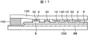
図17に本実施例の構成を示す。図17において、対向基板200の周辺遮光膜220には、3層のカラーフィルタからなる周辺スペーサ30が形成されている。3層のカラーフィルタを使用することによって、本実施例における周辺スペーサ30の高さは実施例3における周辺スペーサよりも高くなっている。また、本実施例において、緑カラーフィルタGおよび青カラーフィルタBを柱状スペーサとしている。そして、柱状の緑カラーフィルタGの面積を周辺に行くほど大きくすることによって、基板周辺側のスペーサの高さを徐々に大きくしている。
FIG. 17 shows the configuration of this embodiment. In FIG. 17, a
図17は、緑カラーフィルタGの面積および高さを変化させているが、スペーサの高さを周辺部においてより大きく変化させたい場合は、柱状の青カラーフィルタBの面積を変えることも出来る。したがって、本実施例においては、周辺のスペーサの高さを変えたい場合に、より設計の自由度を持つことが出来る。 Although the area and height of the green color filter G are changed in FIG. 17, the area of the columnar blue color filter B can be changed when it is desired to change the height of the spacer more greatly in the peripheral portion. Therefore, in this embodiment, when it is desired to change the height of the peripheral spacers, it is possible to have a higher degree of design freedom.
実施例1〜実施例4は対向基板200に液晶を駆動する対向電極201が形成されていない場合を例にとって説明した。しかし、本発明は、対向基板200に対向電極201が形成されている場合の構成に対しても適用できることは先に述べたとおりである。図18はこの構成の例を示す。図18は説明のために、スペーサが形成された部分の断面のみを示す。また、図18は、図7における第1スペーサ10の部分のみを取り出したものである。図18に示す部分以外の構成は、実施例1または、実施例2で説明したものと同様である。
In the first to fourth embodiments, the case where the
図18では、対向基板200が下側で、TFT基板100が上側に配置されている。TFT基板100に形成された配線、TFT等は省略されている。図18において、対向基板200にはブラックマトリクスBMが形成され、ブラックマトリクスBMの両側には青画素BPあるいは赤画素RPが形成されている。ブラックマトリクスBMの上には、赤カラーフィルタR、緑カラーフィルタG、青カラーフィルタBが積層されている。スペーサの高さは、スペーサの面積を変えることによって調整できることは実施例1および実施例2で説明したとおりである。
In FIG. 18, the
本実施例では、対向基板200のオーバーコート膜OCの上に対向電極201が形成されている。対向電極201が柱状スペーサの上にまで形成されていると、TFT基板100とスペーサが接触した際、配向膜106が破壊したりすると、対向電極201とTFT基板100に形成された配線とが接触して、対向電極201とTFT基板100に形成された配線とがショートする可能性がある。本実施例ではこの危険を防止するために、図18に示すように、対向電極201を、スペーサの部分には形成しないようにしている。このように構成することによって、対向基板200に対向電極201を形成する場合にも本発明を実施することが出来る。
In this embodiment, the
以上は、対向基板200に対向電極201が形成されている場合の、第1スペーサ10について本発明を適用する場合を説明したが、第2スペーサ20に適用する場合も同様である。すなわち、第2スペーサ20は第1スペーサ10よりも高さを低くするが、これは、第2スペーサ20においては、カラーフィルタの層を2層にする、あるいは、柱状カラーフィルタの面積を第1スペーサ10の場合よりも小さくすること等によって実現することが出来る。
Although the case where the present invention is applied to the
図19は本発明をいわゆるVA方式の液晶表示装置に適用する例である。図19は説明のために、スペーサが形成された部分の断面のみを示している。また、図19は、図7における第1スペーサ10の部分のみを取り出したものである。図19に示す部分以外の構成は、実施例1または、実施例2で説明したものと同様である。
FIG. 19 shows an example in which the present invention is applied to a so-called VA liquid crystal display device. FIG. 19 shows only a cross section of a portion where a spacer is formed for the sake of explanation. FIG. 19 shows only the portion of the
図19では、対向基板200が下側で、TFT基板100が上側に配置されている。TFT基板100に形成された配線、TFT等は省略されている。図19において、対向基板200にはブラックマトリクスBMが形成され、ブラックマトリクスBMの両側には緑画素GPあるいは赤画素RPが形成されている。ブラックマトリクスBMの上には、赤カラーフィルタR、緑カラーフィルタG、青カラーフィルタBが積層されている。スペーサの高さは、スペーサの面積を変えることによって調整できることは実施例1および実施例2で説明したとおりである。
In FIG. 19, the
本実施例では、スペーサの上にリブ205が設けられている。このリブ205は、画素電極上にも延設して形成され、画素電極上では、液晶分子を傾むかせ、視野角を広げる機能を有する。図19において、スペーサの高さは赤カラーフィルタR、緑カラーフィルタG、青カラーフィルタBを積層することによって形成されていることは実施例1等と同様である。また、スペーサの高さは、スペーサを構成するカラーフィルタの面積を制御する、あるいは、カラーフィルタの積層の方法によるレベリングを利用して制御することが出来ることは実施例1で説明したとおりである。
In this embodiment, a
本実施例が実施例5と異なる点は、対向基板200に形成された対向電極201をカラーフィルタによるスペーサの上にまで形成している点である。すなわち、本実施例においては、カラーフィルタによるスペーサの上に対向電極201を形成しても、TFT基板100との間に、配向膜106に加えて、リブ205が存在しているために、対向電極201とTFT基板100に形成された配線とがショートする確率は非常に小さいために、このような構成をとることが出来る。
The difference between the present embodiment and the fifth embodiment is that the
このように、VA方式においても、本発明を適用することが出来る。以上は、図7における第1スペーサ10について説明したが、第2スペーサ20についても同様に実現できることは実施例5で説明したとおりである。
Thus, the present invention can also be applied to the VA system. Although the
10 第1スペーサ、15 スペーサ台座、20 第2スペーサ、30 周辺スペーサ、100 TFT基板、101 走査線、102 SD電極、103 ゲート絶縁膜、104 a−Si、105 パッシベーション膜、106 配向膜、107 液晶層、130 端子部、150 シール部、200 対向基板、201 対向電極、205 リブ、210 表示領域、220 周辺遮光、1021 映像信号線、1022 台座メタル、R 赤カラーフィルタ、G 緑カラーフィルタ、B 青カラーフィルタ、RP 赤画素、GP 緑画素、BP 青画素、BM ブラックマトリクス、OC オーバーコート膜。 10 First spacer, 15 Spacer base, 20 Second spacer, 30 Peripheral spacer, 100 TFT substrate, 101 Scan line, 102 SD electrode, 103 Gate insulating film, 104 a-Si, 105 Passivation film, 106 Alignment film, 107 Liquid crystal Layer, 130 terminal portion, 150 seal portion, 200 counter substrate, 201 counter electrode, 205 rib, 210 display area, 220 peripheral shading, 1021 video signal line, 1022 base metal, R red color filter, G green color filter, B blue Color filter, RP red pixel, GP green pixel, BP blue pixel, BM black matrix, OC overcoat film.
Claims (9)
前記対向基板には、第1のカラーフィルタによって第1の色を表示する第1の画素が縦方向に配列し、第2のカラーフィルタによって第2の色を表示する第2の画素が縦方向に配列し、第3のカラーフィルタによって第3の色を表示する第3の画素が縦方向に配列し、
前記第1のカラーフィルタは前記第1の画素を覆って縦方向にストライプ状に延在し、
前記第2のカラーフィルタは前記第2の画素を覆って縦方向にストライプ状に延在し、前記第3のカラーフィルタは前記第3の画素を覆って縦方向に延在し、
前記第1の画素と前記第1の画素の間には、前記第1のカラーフィルタを含む複数のカラーフィルタが積層された第1のスペーサが形成され、
第2の画素と前記第2の画素の間には前記第2のカラーフィルタを含む複数のカラーフィルタによって第2のスペーサが形成され、
前記第1のカラーフィルタは、前記第2の画素と前記第2の画素の間に、平面が円形状に形成され、
前記第1のスペーサを構成する前記複数のカラーフィルタのうちの下側のカラーフィルタの面積は、前記上側のカラーフィルタの面積よりも大きく、
前記第2のスペーサを構成する前記複数のカラーフィルタのうちの下側のカラーフィルタの面積は、前記上側のカラーフィルタの面積よりも小さく、
前記下側のカラーフィルタは前記複数のカラーフィルタのうちの最下層のカラーフィルタであり、前記上側のカラーフィルタは前記複数のカラーフィルタのうちの最上層のカラーフィルタであり、
前記第1のスペーサの高さは、前記第2のスペーサの高さよりも大きく、
前記第3のカラーフィルタは、前記第1の画素と前記第1の画素の間と前記第3の画素と前記第3の画素の間をストライプ状に横方向に延在していることを特徴とする液晶表示装置。 A liquid crystal display device in which liquid crystal is sandwiched between a TFT substrate, a counter substrate, and the TFT substrate and the counter substrate,
On the counter substrate, first pixels that display the first color by the first color filter are arranged in the vertical direction, and second pixels that display the second color by the second color filter are arranged in the vertical direction. The third pixels displaying the third color by the third color filter are arranged in the vertical direction,
The first color filter extends in a stripe shape in a vertical direction covering the first pixel,
The second color filter covers the second pixel and extends in a stripe shape in the vertical direction, and the third color filter covers the third pixel and extends in the vertical direction,
Between the first pixel and the first pixel, a first spacer in which a plurality of color filters including the first color filter are stacked is formed,
A second spacer is formed between the second pixel and the second pixel by a plurality of color filters including the second color filter,
The first color filter has a circular plane formed between the second pixel and the second pixel,
The area of the lower color filter of the plurality of color filters constituting the first spacer is larger than the area of the upper color filter,
The area of the lower color filter of the plurality of color filters constituting the second spacer is smaller than the area of the upper color filter,
The lower color filter is a lowermost color filter of the plurality of color filters, and the upper color filter is an uppermost color filter of the plurality of color filters;
The height of the first spacer, much larger than the height of the second spacer,
The third color filter extends in a horizontal direction in a stripe shape between the first pixel and the first pixel and between the third pixel and the third pixel. A liquid crystal display device.
前記第1のスペーサ部分に前記対向電極が形成されていないことを特徴とする請求項1に記載の液晶表示装置。 A counter electrode is formed on the counter substrate,
The liquid crystal display device according to claim 1, wherein the counter electrode is not formed on the first spacer portion.
前記第1のスペーサ部分に前記対向電極が形成され、
前記第1のスペーサ上にリブが設けられていることを特徴とする請求項1に記載の液晶表示装置。 A counter electrode is formed on the counter substrate,
The counter electrode is formed on the first spacer portion;
The liquid crystal display device according to claim 1, wherein a rib is provided on the first spacer.
The liquid crystal display device according to claim 1, wherein a plurality of color filters are stacked between the third pixel and the third pixel.
Priority Applications (1)
| Application Number | Priority Date | Filing Date | Title |
|---|---|---|---|
| JP2012134289A JP5563020B2 (en) | 2012-06-13 | 2012-06-13 | Liquid crystal display |
Applications Claiming Priority (1)
| Application Number | Priority Date | Filing Date | Title |
|---|---|---|---|
| JP2012134289A JP5563020B2 (en) | 2012-06-13 | 2012-06-13 | Liquid crystal display |
Related Parent Applications (1)
| Application Number | Title | Priority Date | Filing Date |
|---|---|---|---|
| JP2007326080A Division JP5174450B2 (en) | 2007-12-18 | 2007-12-18 | Liquid crystal display |
Publications (2)
| Publication Number | Publication Date |
|---|---|
| JP2012168566A JP2012168566A (en) | 2012-09-06 |
| JP5563020B2 true JP5563020B2 (en) | 2014-07-30 |
Family
ID=46972705
Family Applications (1)
| Application Number | Title | Priority Date | Filing Date |
|---|---|---|---|
| JP2012134289A Active JP5563020B2 (en) | 2012-06-13 | 2012-06-13 | Liquid crystal display |
Country Status (1)
| Country | Link |
|---|---|
| JP (1) | JP5563020B2 (en) |
Families Citing this family (2)
| Publication number | Priority date | Publication date | Assignee | Title |
|---|---|---|---|---|
| CN106324915B (en) * | 2015-06-24 | 2020-01-24 | 群创光电股份有限公司 | display panel |
| CN113075811B (en) * | 2020-01-06 | 2023-08-18 | 群创光电股份有限公司 | electronic device |
Family Cites Families (5)
| Publication number | Priority date | Publication date | Assignee | Title |
|---|---|---|---|---|
| JP3953588B2 (en) * | 1996-07-16 | 2007-08-08 | 大日本印刷株式会社 | Color filter and liquid crystal display device using the same |
| JP2000258617A (en) * | 1999-03-10 | 2000-09-22 | Toray Ind Inc | Color filter and its production |
| JP2001305328A (en) * | 2000-04-18 | 2001-10-31 | Toray Ind Inc | Method for manufacturing color filter and color filter |
| JP3891865B2 (en) * | 2002-02-07 | 2007-03-14 | 奇美電子股▲ふん▼有限公司 | Liquid crystal display device and color filter substrate thereof |
| JP4134106B2 (en) * | 2004-06-11 | 2008-08-13 | シャープ株式会社 | Color filter substrate, manufacturing method thereof, and display device including the same |
-
2012
- 2012-06-13 JP JP2012134289A patent/JP5563020B2/en active Active
Also Published As
| Publication number | Publication date |
|---|---|
| JP2012168566A (en) | 2012-09-06 |
Similar Documents
| Publication | Publication Date | Title |
|---|---|---|
| JP5174450B2 (en) | Liquid crystal display | |
| JP5553531B2 (en) | Liquid crystal display | |
| CN100395638C (en) | LCD Monitor | |
| JP2009069391A (en) | Liquid crystal display device | |
| JP5840873B2 (en) | Mother board | |
| JP6203575B2 (en) | Display device | |
| JP2017090528A (en) | Display device | |
| JP2009204681A (en) | Liquid crystal display | |
| JP6649788B2 (en) | Liquid crystal display | |
| US20170115525A1 (en) | Liquid crystal display device | |
| JP6591194B2 (en) | Liquid crystal display device | |
| JP2016080797A (en) | Liquid crystal display | |
| KR20140119912A (en) | Thin film transistor liquid crystal display device | |
| JP2017167478A (en) | Liquid crystal display device and mother substrate for the same | |
| JP2012098329A (en) | Liquid crystal display device | |
| WO2012124662A1 (en) | Liquid crystal display | |
| JP5563020B2 (en) | Liquid crystal display | |
| JP2017187530A (en) | Liquid crystal display | |
| JP2017122790A (en) | Liquid crystal display | |
| WO2012124699A1 (en) | Liquid crystal display | |
| JP5323329B2 (en) | Liquid crystal display | |
| JP2017076010A (en) | Display device | |
| JP2017076009A (en) | Display device | |
| JP4987585B2 (en) | Liquid crystal display | |
| WO2021070492A1 (en) | Liquid crystal display device |
Legal Events
| Date | Code | Title | Description |
|---|---|---|---|
| A621 | Written request for application examination |
Free format text: JAPANESE INTERMEDIATE CODE: A621 Effective date: 20120613 |
|
| A977 | Report on retrieval |
Free format text: JAPANESE INTERMEDIATE CODE: A971007 Effective date: 20130321 |
|
| A131 | Notification of reasons for refusal |
Free format text: JAPANESE INTERMEDIATE CODE: A131 Effective date: 20130326 |
|
| A521 | Request for written amendment filed |
Free format text: JAPANESE INTERMEDIATE CODE: A523 Effective date: 20130509 |
|
| A131 | Notification of reasons for refusal |
Free format text: JAPANESE INTERMEDIATE CODE: A131 Effective date: 20131224 |
|
| A521 | Request for written amendment filed |
Free format text: JAPANESE INTERMEDIATE CODE: A523 Effective date: 20140204 |
|
| TRDD | Decision of grant or rejection written | ||
| A01 | Written decision to grant a patent or to grant a registration (utility model) |
Free format text: JAPANESE INTERMEDIATE CODE: A01 Effective date: 20140603 |
|
| A61 | First payment of annual fees (during grant procedure) |
Free format text: JAPANESE INTERMEDIATE CODE: A61 Effective date: 20140611 |
|
| R150 | Certificate of patent or registration of utility model |
Ref document number: 5563020 Country of ref document: JP Free format text: JAPANESE INTERMEDIATE CODE: R150 |
|
| R250 | Receipt of annual fees |
Free format text: JAPANESE INTERMEDIATE CODE: R250 |
|
| R250 | Receipt of annual fees |
Free format text: JAPANESE INTERMEDIATE CODE: R250 |
|
| R250 | Receipt of annual fees |
Free format text: JAPANESE INTERMEDIATE CODE: R250 |
|
| R250 | Receipt of annual fees |
Free format text: JAPANESE INTERMEDIATE CODE: R250 |
|
| R250 | Receipt of annual fees |
Free format text: JAPANESE INTERMEDIATE CODE: R250 |
|
| R250 | Receipt of annual fees |
Free format text: JAPANESE INTERMEDIATE CODE: R250 |
|
| R250 | Receipt of annual fees |
Free format text: JAPANESE INTERMEDIATE CODE: R250 |
|
| S111 | Request for change of ownership or part of ownership |
Free format text: JAPANESE INTERMEDIATE CODE: R313113 |
|
| R350 | Written notification of registration of transfer |
Free format text: JAPANESE INTERMEDIATE CODE: R350 |
|
| R250 | Receipt of annual fees |
Free format text: JAPANESE INTERMEDIATE CODE: R250 |