JP5510631B2 - Hexagonal wurtzite compound single crystal and method for producing the same - Google Patents
Hexagonal wurtzite compound single crystal and method for producing the same Download PDFInfo
- Publication number
- JP5510631B2 JP5510631B2 JP2009049503A JP2009049503A JP5510631B2 JP 5510631 B2 JP5510631 B2 JP 5510631B2 JP 2009049503 A JP2009049503 A JP 2009049503A JP 2009049503 A JP2009049503 A JP 2009049503A JP 5510631 B2 JP5510631 B2 JP 5510631B2
- Authority
- JP
- Japan
- Prior art keywords
- crystal
- single crystal
- hexagonal wurtzite
- growth
- compound single
- Prior art date
- Legal status (The legal status is an assumption and is not a legal conclusion. Google has not performed a legal analysis and makes no representation as to the accuracy of the status listed.)
- Active
Links
- 239000013078 crystal Substances 0.000 title claims description 327
- 229910052984 zinc sulfide Inorganic materials 0.000 title claims description 73
- 150000001875 compounds Chemical class 0.000 title claims description 66
- 238000004519 manufacturing process Methods 0.000 title description 22
- 239000000758 substrate Substances 0.000 claims description 44
- 238000000034 method Methods 0.000 claims description 43
- 239000011159 matrix material Substances 0.000 claims description 22
- 239000000463 material Substances 0.000 claims description 17
- 230000005540 biological transmission Effects 0.000 claims description 10
- 238000002441 X-ray diffraction Methods 0.000 claims description 8
- 229910003363 ZnMgO Inorganic materials 0.000 claims description 5
- XLOMVQKBTHCTTD-UHFFFAOYSA-N Zinc monoxide Chemical compound [Zn]=O XLOMVQKBTHCTTD-UHFFFAOYSA-N 0.000 description 182
- 239000011787 zinc oxide Substances 0.000 description 86
- KWYUFKZDYYNOTN-UHFFFAOYSA-M Potassium hydroxide Chemical compound [OH-].[K+] KWYUFKZDYYNOTN-UHFFFAOYSA-M 0.000 description 29
- WMFOQBRAJBCJND-UHFFFAOYSA-M Lithium hydroxide Chemical compound [Li+].[OH-] WMFOQBRAJBCJND-UHFFFAOYSA-M 0.000 description 27
- MHAJPDPJQMAIIY-UHFFFAOYSA-N Hydrogen peroxide Chemical compound OO MHAJPDPJQMAIIY-UHFFFAOYSA-N 0.000 description 20
- 238000001027 hydrothermal synthesis Methods 0.000 description 20
- 239000002994 raw material Substances 0.000 description 20
- 230000008646 thermal stress Effects 0.000 description 17
- 239000010409 thin film Substances 0.000 description 17
- 230000007547 defect Effects 0.000 description 15
- 230000000694 effects Effects 0.000 description 15
- 230000008569 process Effects 0.000 description 15
- 230000015572 biosynthetic process Effects 0.000 description 14
- BASFCYQUMIYNBI-UHFFFAOYSA-N platinum Chemical compound [Pt] BASFCYQUMIYNBI-UHFFFAOYSA-N 0.000 description 13
- 229910052760 oxygen Inorganic materials 0.000 description 12
- QVGXLLKOCUKJST-UHFFFAOYSA-N atomic oxygen Chemical compound [O] QVGXLLKOCUKJST-UHFFFAOYSA-N 0.000 description 11
- 239000001301 oxygen Substances 0.000 description 11
- 238000010586 diagram Methods 0.000 description 10
- 230000035882 stress Effects 0.000 description 10
- 239000012670 alkaline solution Substances 0.000 description 9
- 230000007423 decrease Effects 0.000 description 9
- 239000010408 film Substances 0.000 description 8
- 238000005498 polishing Methods 0.000 description 8
- JMASRVWKEDWRBT-UHFFFAOYSA-N Gallium nitride Chemical compound [Ga]#N JMASRVWKEDWRBT-UHFFFAOYSA-N 0.000 description 7
- 230000000630 rising effect Effects 0.000 description 7
- 241000894007 species Species 0.000 description 7
- XLYOFNOQVPJJNP-UHFFFAOYSA-N water Substances O XLYOFNOQVPJJNP-UHFFFAOYSA-N 0.000 description 7
- 239000011701 zinc Substances 0.000 description 7
- 229910002601 GaN Inorganic materials 0.000 description 6
- 239000007864 aqueous solution Substances 0.000 description 6
- 238000004090 dissolution Methods 0.000 description 6
- 238000011156 evaluation Methods 0.000 description 6
- 239000012535 impurity Substances 0.000 description 6
- 238000005259 measurement Methods 0.000 description 6
- 229910052697 platinum Inorganic materials 0.000 description 6
- 239000003513 alkali Substances 0.000 description 5
- 230000000052 comparative effect Effects 0.000 description 5
- 239000007800 oxidant agent Substances 0.000 description 5
- 239000002245 particle Substances 0.000 description 5
- 238000005424 photoluminescence Methods 0.000 description 5
- 239000000243 solution Substances 0.000 description 5
- 230000002411 adverse Effects 0.000 description 4
- 238000006243 chemical reaction Methods 0.000 description 4
- 239000007789 gas Substances 0.000 description 4
- 238000010438 heat treatment Methods 0.000 description 4
- 150000002500 ions Chemical class 0.000 description 4
- 239000002904 solvent Substances 0.000 description 4
- 238000000992 sputter etching Methods 0.000 description 4
- 229910052725 zinc Inorganic materials 0.000 description 4
- 239000005083 Zinc sulfide Substances 0.000 description 3
- 229910045601 alloy Inorganic materials 0.000 description 3
- 239000000956 alloy Substances 0.000 description 3
- 238000004458 analytical method Methods 0.000 description 3
- 239000012153 distilled water Substances 0.000 description 3
- 238000005516 engineering process Methods 0.000 description 3
- 239000007791 liquid phase Substances 0.000 description 3
- 230000003287 optical effect Effects 0.000 description 3
- 238000001556 precipitation Methods 0.000 description 3
- 238000004729 solvothermal method Methods 0.000 description 3
- 239000012808 vapor phase Substances 0.000 description 3
- QGZKDVFQNNGYKY-UHFFFAOYSA-N Ammonia Chemical group N QGZKDVFQNNGYKY-UHFFFAOYSA-N 0.000 description 2
- IJGRMHOSHXDMSA-UHFFFAOYSA-N Atomic nitrogen Chemical compound N#N IJGRMHOSHXDMSA-UHFFFAOYSA-N 0.000 description 2
- HCHKCACWOHOZIP-UHFFFAOYSA-N Zinc Chemical compound [Zn] HCHKCACWOHOZIP-UHFFFAOYSA-N 0.000 description 2
- 230000001133 acceleration Effects 0.000 description 2
- 238000011161 development Methods 0.000 description 2
- 230000005684 electric field Effects 0.000 description 2
- 230000005284 excitation Effects 0.000 description 2
- 239000010931 gold Substances 0.000 description 2
- 238000003384 imaging method Methods 0.000 description 2
- APFVFJFRJDLVQX-UHFFFAOYSA-N indium atom Chemical compound [In] APFVFJFRJDLVQX-UHFFFAOYSA-N 0.000 description 2
- 239000011810 insulating material Substances 0.000 description 2
- 239000013081 microcrystal Substances 0.000 description 2
- 238000001451 molecular beam epitaxy Methods 0.000 description 2
- 150000004767 nitrides Chemical class 0.000 description 2
- 230000006911 nucleation Effects 0.000 description 2
- 238000010899 nucleation Methods 0.000 description 2
- 238000012856 packing Methods 0.000 description 2
- SBIBMFFZSBJNJF-UHFFFAOYSA-N selenium;zinc Chemical compound [Se]=[Zn] SBIBMFFZSBJNJF-UHFFFAOYSA-N 0.000 description 2
- VYPSYNLAJGMNEJ-UHFFFAOYSA-N silicon dioxide Inorganic materials O=[Si]=O VYPSYNLAJGMNEJ-UHFFFAOYSA-N 0.000 description 2
- 239000007858 starting material Substances 0.000 description 2
- 238000010897 surface acoustic wave method Methods 0.000 description 2
- 230000007704 transition Effects 0.000 description 2
- 229910002704 AlGaN Inorganic materials 0.000 description 1
- PIGFYZPCRLYGLF-UHFFFAOYSA-N Aluminum nitride Chemical compound [Al]#N PIGFYZPCRLYGLF-UHFFFAOYSA-N 0.000 description 1
- 206010021143 Hypoxia Diseases 0.000 description 1
- -1 InN Chemical compound 0.000 description 1
- BUGBHKTXTAQXES-UHFFFAOYSA-N Selenium Chemical compound [Se] BUGBHKTXTAQXES-UHFFFAOYSA-N 0.000 description 1
- NINIDFKCEFEMDL-UHFFFAOYSA-N Sulfur Chemical compound [S] NINIDFKCEFEMDL-UHFFFAOYSA-N 0.000 description 1
- 235000005811 Viola adunca Nutrition 0.000 description 1
- 240000009038 Viola odorata Species 0.000 description 1
- 235000013487 Viola odorata Nutrition 0.000 description 1
- 235000002254 Viola papilionacea Nutrition 0.000 description 1
- 229910021529 ammonia Inorganic materials 0.000 description 1
- 238000013459 approach Methods 0.000 description 1
- 239000003125 aqueous solvent Substances 0.000 description 1
- 239000000919 ceramic Substances 0.000 description 1
- 229910010293 ceramic material Inorganic materials 0.000 description 1
- 238000003486 chemical etching Methods 0.000 description 1
- 239000003795 chemical substances by application Substances 0.000 description 1
- 239000008119 colloidal silica Substances 0.000 description 1
- 239000004020 conductor Substances 0.000 description 1
- 238000007796 conventional method Methods 0.000 description 1
- 238000001816 cooling Methods 0.000 description 1
- PMHQVHHXPFUNSP-UHFFFAOYSA-M copper(1+);methylsulfanylmethane;bromide Chemical compound Br[Cu].CSC PMHQVHHXPFUNSP-UHFFFAOYSA-M 0.000 description 1
- RKTYLMNFRDHKIL-UHFFFAOYSA-N copper;5,10,15,20-tetraphenylporphyrin-22,24-diide Chemical compound [Cu+2].C1=CC(C(=C2C=CC([N-]2)=C(C=2C=CC=CC=2)C=2C=CC(N=2)=C(C=2C=CC=CC=2)C2=CC=C3[N-]2)C=2C=CC=CC=2)=NC1=C3C1=CC=CC=C1 RKTYLMNFRDHKIL-UHFFFAOYSA-N 0.000 description 1
- 238000002109 crystal growth method Methods 0.000 description 1
- 230000003247 decreasing effect Effects 0.000 description 1
- 230000006866 deterioration Effects 0.000 description 1
- 239000010432 diamond Substances 0.000 description 1
- 229910003460 diamond Inorganic materials 0.000 description 1
- 239000006185 dispersion Substances 0.000 description 1
- 238000005530 etching Methods 0.000 description 1
- 238000011049 filling Methods 0.000 description 1
- 239000007888 film coating Substances 0.000 description 1
- 238000009501 film coating Methods 0.000 description 1
- PCHJSUWPFVWCPO-UHFFFAOYSA-N gold Chemical compound [Au] PCHJSUWPFVWCPO-UHFFFAOYSA-N 0.000 description 1
- 229910052737 gold Inorganic materials 0.000 description 1
- 230000017525 heat dissipation Effects 0.000 description 1
- 230000020169 heat generation Effects 0.000 description 1
- 238000000097 high energy electron diffraction Methods 0.000 description 1
- 230000006872 improvement Effects 0.000 description 1
- 229910001026 inconel Inorganic materials 0.000 description 1
- 229910052738 indium Inorganic materials 0.000 description 1
- 230000005764 inhibitory process Effects 0.000 description 1
- 229910052744 lithium Inorganic materials 0.000 description 1
- 238000000691 measurement method Methods 0.000 description 1
- 230000007246 mechanism Effects 0.000 description 1
- 239000000155 melt Substances 0.000 description 1
- 229910052757 nitrogen Inorganic materials 0.000 description 1
- 231100000989 no adverse effect Toxicity 0.000 description 1
- 238000006116 polymerization reaction Methods 0.000 description 1
- 230000002980 postoperative effect Effects 0.000 description 1
- CHWRSCGUEQEHOH-UHFFFAOYSA-N potassium oxide Chemical compound [O-2].[K+].[K+] CHWRSCGUEQEHOH-UHFFFAOYSA-N 0.000 description 1
- 229910001950 potassium oxide Inorganic materials 0.000 description 1
- 238000005036 potential barrier Methods 0.000 description 1
- 239000000843 powder Substances 0.000 description 1
- 238000010298 pulverizing process Methods 0.000 description 1
- 238000011002 quantification Methods 0.000 description 1
- 239000010453 quartz Substances 0.000 description 1
- 230000009467 reduction Effects 0.000 description 1
- 238000002128 reflection high energy electron diffraction Methods 0.000 description 1
- 238000011160 research Methods 0.000 description 1
- 238000007789 sealing Methods 0.000 description 1
- 229910052711 selenium Inorganic materials 0.000 description 1
- 239000011669 selenium Substances 0.000 description 1
- 239000004065 semiconductor Substances 0.000 description 1
- 150000003384 small molecules Chemical class 0.000 description 1
- 239000007790 solid phase Substances 0.000 description 1
- 238000001228 spectrum Methods 0.000 description 1
- 229910052950 sphalerite Inorganic materials 0.000 description 1
- 229910052717 sulfur Inorganic materials 0.000 description 1
- 239000011593 sulfur Substances 0.000 description 1
- 230000001629 suppression Effects 0.000 description 1
- 239000002344 surface layer Substances 0.000 description 1
- 239000000725 suspension Substances 0.000 description 1
- 238000001947 vapour-phase growth Methods 0.000 description 1
- 230000000007 visual effect Effects 0.000 description 1
- 150000003752 zinc compounds Chemical class 0.000 description 1
- DRDVZXDWVBGGMH-UHFFFAOYSA-N zinc;sulfide Chemical compound [S-2].[Zn+2] DRDVZXDWVBGGMH-UHFFFAOYSA-N 0.000 description 1
Images


Landscapes
- Inorganic Compounds Of Heavy Metals (AREA)
- Crystals, And After-Treatments Of Crystals (AREA)
Description
本発明は、六方晶系ウルツ鉱型化合物単結晶及びその製造方法に関し、より詳細には、六方晶系ウルツ鉱型化合物単結晶及びその製造方法並びにエピタキシャル成長用単結晶基板に関する。 The present invention relates to a hexagonal wurtzite compound single crystal and a method for producing the same, and more particularly to a hexagonal wurtzite compound single crystal, a method for producing the same, and a single crystal substrate for epitaxial growth.
一般に、六方晶系の結晶は、正六角形の平面内で120゜をなす3本のa軸と、それらのa軸に垂直なc軸とを合わせて4本の結晶軸を有している。 In general, a hexagonal crystal has four crystal axes including three a axes forming 120 ° in a regular hexagonal plane and a c axis perpendicular to the a axis.
図1(a)乃至(c)は、六方晶系の結晶を示す図で、図1(a)は斜視図、図1(b)は図1(a)の上面図、図1(c)は図1(b)のm面の正面図である。図1(a)に示すように、c軸に垂直な(0001)面をc面と呼び、c軸と任意のa軸に平行な面をm面と呼び、図1(b)に示すように、c軸に平行で任意のa軸に垂直な面をa面と呼んでいる。a面とm面は、c面に垂直で、c軸方向と平行な面である。また、m面を正面から見ると、図1(c)に示すようになり、c面を横からみた場合の結晶格子が見える。 1A to 1C are diagrams showing hexagonal crystals, FIG. 1A is a perspective view, FIG. 1B is a top view of FIG. 1A, and FIG. FIG. 2 is a front view of the m-plane in FIG. As shown in FIG. 1A, the (0001) plane perpendicular to the c-axis is called the c-plane, and the plane parallel to the c-axis and any a-axis is called the m-plane, as shown in FIG. In addition, a plane parallel to the c-axis and perpendicular to the arbitrary a-axis is called an a-plane. The a-plane and m-plane are planes perpendicular to the c-plane and parallel to the c-axis direction. Further, when the m-plane is viewed from the front, it becomes as shown in FIG. 1C, and the crystal lattice when the c-plane is viewed from the side can be seen.
六方晶系のうち、AX(Aは陽性元素、Xは陰性元素)で示される化合物に見られる結晶構造、すなわち、ウルツ鉱型構造の原子配列はA原子とX原子はそれぞれ六方最密構造型に近い配列をとり、A原子にはX原子4個が正四面体形に配位し、逆にX原子にもA原子4個が正四面体形に配位している。 Among the hexagonal crystal systems, the crystal structure found in the compound represented by AX (A is a positive element, X is a negative element), that is, the atomic arrangement of the wurtzite structure is that the A atom and the X atom are hexagonal close-packed structures, respectively. The A atom has four X atoms coordinated in a regular tetrahedral shape, and the X atom has four A atoms coordinated in a tetrahedral shape.
それぞれの正四面体クラスタで、図1(a)に示すように、c軸に平行な方向のうちAの直上にXがある方向を+c、図1(b)に示すように、Xの直上にAがある方向を−cと呼び、c軸に垂直なc面であって+cおよび−c方向を、それぞれ(0001)面、(000−1)面と書いて区別する。c面を切り出す場合には、図1(c)に示すように、(0001)面では元素A、(000−1)面では元素Xのみが表面に現れる。成長後の単結晶の場合も表面は同様になる。 In each tetrahedral cluster, as shown in FIG. 1 (a), the direction parallel to the c-axis with X immediately above A is + c, and as shown in FIG. 1 (b), directly above X. The direction in which A is present is called -c, and the c-plane perpendicular to the c-axis and + c and -c directions are written as (0001) plane and (000-1) plane, respectively. When the c-plane is cut out, as shown in FIG. 1C, only the element A appears on the (0001) plane and only the element X appears on the (000-1) plane. The surface of the single crystal after growth is the same.
このような原子配列を取るために、ウルツ鉱型構造ではc軸方向に極性を有する。六方晶系ウルツ鉱型構造をとることが知られている化合物としては、ウルツ鉱である硫化亜鉛(ZnS)をはじめ、酸化亜鉛(ZnO)、窒化アルミニウム(AlN)、窒化ガリウム(GaN)、窒化インジウム(InN)などが挙げられる。 In order to take such an atomic arrangement, the wurtzite structure has polarity in the c-axis direction. Compounds known to have a hexagonal wurtzite structure include wurtzite zinc sulfide (ZnS), zinc oxide (ZnO), aluminum nitride (AlN), gallium nitride (GaN), and nitride. Indium (InN) and the like can be given.
六方晶系ウルツ鉱型化合物単結晶の成長方法としては、気相法、液相法、融液法があるが、気相法、融液法ではそれぞれ欠陥密度が高い、成長に非常に高圧、高温を要するなどの欠点がある。これに対して液相法は、欠陥密度の低い高品位の結晶が比較的低い温度で得られるという特徴がある。中でもソルボサーマル法は欠陥や不純物濃度の低い高品位の結晶成長に適しているといわれている。ソルボサーマル法とは、超臨界状態の溶媒を保持する容器中に、原料と種結晶を装填し、温度差を利用して原料溶解、再析出させて単結晶を得る方法の総称であり、溶媒が水である場合は水熱法、アンモニアである場合はアモノサーマル法と呼ばれる。 Hexagonal wurtzite compound single crystal growth methods include vapor phase method, liquid phase method, and melt method, but the vapor phase method and melt method each have high defect density, very high pressure for growth, There are drawbacks such as requiring high temperatures. In contrast, the liquid phase method is characterized in that high-quality crystals with a low defect density can be obtained at a relatively low temperature. In particular, the solvothermal method is said to be suitable for high-quality crystal growth with low defects and impurity concentrations. The solvothermal method is a general term for a method of obtaining a single crystal by charging a raw material and a seed crystal in a container holding a supercritical solvent, and dissolving and reprecipitating the raw material using a temperature difference. When is water, it is called a hydrothermal method, and when it is ammonia, it is called an ammonothermal method.
六方晶系ウルツ鉱型化合物は、直接遷移型のバンドギャップであること、電子移動度が大きいこと、バンドギャップが狭い材料から広い材料まで連続的に形成し得ることから、近年、既に実用化されているGaN系LEDに続き、紫外や緑色のLED,LD,パワーデバイス,高周波デバイスなどへの展開が期待されている。 Hexagonal wurtzite-type compounds have already been put into practical use in recent years because of their direct transition type band gap, high electron mobility, and ability to continuously form materials with narrow band gaps to wide materials. Following GaN-based LEDs, development to ultraviolet and green LEDs, LDs, power devices, high-frequency devices and the like is expected.
しかしながら、六方晶系ウルツ鉱型結晶を形成する一方の元素である陰性元素は窒素や酸素などの分子ガスもしくは硫黄やセレンなどの揮発性を有する元素であり、結晶成長時に陽性元素との組成を量論比に保つことが困難である。そのため、ソルボサーマル法が密封された高圧容器内で陰性元素成分を含む環境で結晶成長が可能であることを利用して陰性元素が結晶中に欠落する欠陥の発生を抑える検討が成されてきた結果、一定度の成果が得られ、例えば、X線回折における(0002)面のロッキングカーブの半値幅は顕著な改善が成されてきた。 However, the negative element, which is one of the elements forming the hexagonal wurtzite crystal, is a molecular gas such as nitrogen or oxygen or a volatile element such as sulfur or selenium. It is difficult to maintain a stoichiometric ratio. For this reason, studies have been made to suppress the occurrence of defects in which negative elements are missing in the crystal by utilizing the fact that crystal growth is possible in an environment containing negative element components in a high-pressure vessel sealed by the solvothermal method. As a result, a certain degree of result was obtained. For example, the half-value width of the rocking curve of the (0002) plane in X-ray diffraction has been remarkably improved.
しかしながら、それでもなお、大きな欠陥である転位欠陥密度は期待に反して悪化し、さらには熱や応力が加わった際に転位やクラックが発生する課題があるが、全く手が付けられていないのが現状である。全ての課題を解決するユニバーサルな手法は、全く欠陥の無い完全結晶を得ることであるが、上述した六方晶系ウルツ鉱型結晶の特徴を踏まえると非常に難しく現実的な手法とは言えない。 Nevertheless, dislocation defect density, which is a large defect, deteriorates unexpectedly, and there is a problem that dislocations and cracks occur when heat and stress are applied, but it is not handled at all. Currently. A universal method for solving all the problems is to obtain a complete crystal having no defects at all, but it is not very difficult and practical based on the characteristics of the hexagonal wurtzite crystal described above.
以下、六方晶系ウルツ鉱型の結晶構造を有する化合物のうち酸化亜鉛(以下、ZnOという)単結晶、更に詳しくは、青紫、紫外発光素子(用基板),表面弾性波(SAW),ガスセンサ,圧電素子,透明導電体,バリスタなど多方面に用いられ、優れた機能を発現するZnO単結晶とそれを用いた基板を中心に説明する。ただし、本発明の六方晶系ウルツ鉱型化合物単結晶はZnOに限定されるものではない。 Hereinafter, among the compounds having a hexagonal wurtzite crystal structure, zinc oxide (hereinafter referred to as ZnO) single crystal, more specifically, blue-violet, ultraviolet light emitting element (substrate), surface acoustic wave (SAW), gas sensor, The description will focus on a ZnO single crystal that is used in various fields such as a piezoelectric element, a transparent conductor, and a varistor and exhibits an excellent function, and a substrate using the ZnO single crystal. However, the hexagonal wurtzite compound single crystal of the present invention is not limited to ZnO.
酸化亜鉛(ZnO)は、六方晶系のウルツ鉱型化合物の結晶構造を持ち、直接遷移で禁制帯幅が3.37eVと大きく、かつ励起子結合エネルギー(ZnO:60meV)が他の化合物半導体材料と比べて非常に大きく(GaN:26eV、ZnSe:20eV等)、励起子が発光デバイスの通常の作動温度範囲で有効である。そのため、ZnOをベースとする酸化亜鉛系材料(ZnO、ZnMgO、ZnCdO、ZnCuO等)は、高効率な発光デバイス材料として期待されている。励起子結合エネルギーが非常に高いことは、例えば、発光デバイスに大電流を流して使用する場合の発熱や、大面積化して放熱が悪くなり、デバイス温度が上昇しても発光エネルギー効率が低下しないと言う重要なメリットも有する。 Zinc oxide (ZnO) has a crystal structure of a hexagonal wurtzite compound, a direct transition has a large forbidden band of 3.37 eV, and an exciton binding energy (ZnO: 60 meV) is another compound semiconductor material. Is very large (GaN: 26 eV, ZnSe: 20 eV, etc.), and excitons are effective in the normal operating temperature range of the light emitting device. Therefore, zinc oxide-based materials (ZnO, ZnMgO, ZnCdO, ZnCuO, etc.) based on ZnO are expected as highly efficient light-emitting device materials. The exciton binding energy is very high, for example, heat generation when using a large current in a light-emitting device, and heat dissipation due to a large area is not good, and the light emission energy efficiency does not decrease even if the device temperature rises. It also has an important merit.
一方、ZnOはGaNと同じ結晶構造で格子定数も近い(格子ミスマッチは約2%)こと、GaN単結晶よりも格段に低コストで製造できる可能性があることから、現在用いられているサファイアやSiCに代わるGaN薄膜成長用の基板としても期待を集めている。 On the other hand, ZnO has the same crystal structure as GaN and has a close lattice constant (lattice mismatch is about 2%), and can be manufactured at a much lower cost than GaN single crystals. It is also expected as a substrate for GaN thin film growth that replaces SiC.
酸化亜鉛系材料の発光デバイスを形成するには、薄膜を形成するための単結晶基板が必要である。酸化亜鉛の単結晶成長は古くから研究され、固相成長法であるメルト法、気相成長法であるVPT法、液相成長法である水熱法等があるが、得られる結晶の結晶性、結晶成長速度、設備コスト等の観点から、人工水晶の生産で既に広く知られている水熱成長による成長が最も注目され、多くの検討が行われてきた。例えば、非特許文献1、2には水熱法によるZnO単結晶成長の基本技術が記載されており、その成長法によれば、ZnOの焼結体を結晶の育成容器の下部に、ZnO種結晶を該育成容器の上部に各々配置し、次いでKOH及びLiOHからなるアルカリ水溶液の溶媒を充填する。さらに酸素発生剤として過酸化水素を加えた状態で、育成容器内を370〜400℃の育成温度、700〜1000kg/cm2の圧力で、育成容器内の上部と下部で下部の温度が上部の温度より10〜15℃高くなるように運転することで、種結晶上に酸化亜鉛単結晶を成長させる。 In order to form a light emitting device of a zinc oxide-based material, a single crystal substrate for forming a thin film is required. Single crystal growth of zinc oxide has been studied for a long time, and includes the melt method, which is a solid phase growth method, the VPT method, which is a vapor phase growth method, and the hydrothermal method, which is a liquid phase growth method. From the viewpoint of crystal growth rate, equipment cost, etc., growth by hydrothermal growth, which is already widely known in the production of artificial quartz, has received the most attention and many studies have been conducted. For example, Non-Patent Documents 1 and 2 describe a basic technique of ZnO single crystal growth by a hydrothermal method, and according to the growth method, a ZnO sintered body is placed under a crystal growth container at a ZnO seed. Crystals are respectively placed on top of the growth vessel and then filled with a solvent of an alkaline aqueous solution consisting of KOH and LiOH. Further, in a state where hydrogen peroxide is added as an oxygen generator, the growth temperature in the growth vessel is 370 to 400 ° C. and the pressure is 700 to 1000 kg / cm 2 . By operating so as to be higher by 10 to 15 ° C. than the temperature, a zinc oxide single crystal is grown on the seed crystal.
この報告を基にして多くの研究が成されてきた。例えば、ZnOは酸素欠損起きやすく、0002方向の結晶性が十分でないために、過酸化処理した原料を用い、加えて新たな酸化剤が提案され、X線回折の0002面の半値幅で15arcsecと言う高い結晶性を持つZnO単結晶が開示されている(例えば、特許文献1参照)。また、水熱法によって形成されたZnO基板は、約1cm四方の大きさで既に試験的に販売されており、それらZnO基板のX線回折における0002面の半値幅は、10〜20arcsecと良好な値が得られている(例えば、非特許文献3参照)。 A lot of research has been done based on this report. For example, since ZnO is prone to oxygen deficiency and the crystallinity in the 0002 direction is not sufficient, a new oxidizing agent has been proposed using a peroxidized raw material, and the half-value width of the 0002 plane of X-ray diffraction is 15 arcsec. A ZnO single crystal having high crystallinity is disclosed (see, for example, Patent Document 1). In addition, ZnO substrates formed by the hydrothermal method have already been experimentally sold in a size of about 1 cm square, and the half-value width of the 0002 plane in X-ray diffraction of these ZnO substrates is as good as 10 to 20 arcsec. The value is obtained (for example, refer nonpatent literature 3).
しかしながら、これら従来技術で得られているZnO単結晶は、X線回折で観測した結晶性は改善されているが、多くの転位欠陥を含有しているという問題があった。単結晶基板に転位が存在すると、基板上に薄膜を形成した場合にそれが薄膜へ引き継がれ、電流のリーク等の問題をもたらす。また、転位が多く存在すると、デバイスとして作動中に温度が上昇した際に転位が増殖し、デバイス機能が失われる等の問題が生じる。 However, the ZnO single crystals obtained by these conventional techniques have improved crystallinity observed by X-ray diffraction, but have a problem that they contain many dislocation defects. When dislocations exist in a single crystal substrate, when a thin film is formed on the substrate, it is transferred to the thin film, causing problems such as current leakage. In addition, when there are many dislocations, the dislocation grows when the temperature rises during operation as a device, causing problems such as loss of device function.
一方、従来水熱法によるZnO単結晶成長ではKOHとLiOHの両方を硬化剤として用いるのが一般的であり、それによりc面、m面の両方向に成長した良好な結晶性のZnO単結晶が得られる。しかし、ここで用いたLiのイオン半径がZnと非常に近い事もあり、Liは成長したZnO単結晶中に取り込まれる。ZnOをベースとした発光デバイスを形成しようとした際に、Liが熱や電場で結晶中を移動してしまい、ZnOのp型化を阻害する、薄膜の電気特性を不安定化する等の問題が指摘されている。そのため、特許文献2には、Liを用いず、代わりにNH4OHを用いる技術が、特許文献3には水熱法によって得たZnO単結晶を熱処理して含有するLiを表層部に移動させ、表面をエッチングして結晶内Liを低減する技術が開示されている。 On the other hand, in the conventional ZnO single crystal growth by the hydrothermal method, it is common to use both KOH and LiOH as curing agents, so that a good crystalline ZnO single crystal grown in both the c-plane and m-plane directions can be obtained. can get. However, since the ionic radius of Li used here is very close to that of Zn, Li is taken into the grown ZnO single crystal. When trying to form a light-emitting device based on ZnO, Li moves through the crystal with heat or electric field, which obstructs ZnO p-type formation and destabilizes the electrical properties of the thin film. Has been pointed out. Therefore, Patent Document 2 discloses a technique using NH 4 OH instead of Li, and Patent Document 3 moves Li containing a ZnO single crystal obtained by a hydrothermal method by heat treatment to the surface layer portion. A technique for etching the surface to reduce Li in the crystal is disclosed.
しかし、特許文献2ではLi含有量は顕著に低減するものの、結晶性が大きく低下してしまい、特許文献3では結晶性は良好であるものの、Liは1015/cm3程度までしか低減していない。 However, in Patent Document 2, although the Li content is significantly reduced, the crystallinity is greatly reduced. In Patent Document 3, although the crystallinity is good, Li is reduced only to about 10 15 / cm 3. Absent.
ZnO材料は、従来のデバイス材料と比較して応力、特に熱応力に弱い材料である。そのため、例えば、ZnO基板上に薄膜成長させる場合、基板を周囲から押え付けて応力が掛かった状態で温度を上げると、透過電子顕微鏡レベルで観測される転位が発生し、場合によっては光学顕微鏡で観測される程度のクラックが発生する。成膜時に限らず、ウエハープロセス工程、発光デバイス動作時にも、基板に応力が加わった状態で温度が上がれば、転位等の機械的欠陥を生じる。そのため、転位が少ない基板を用いても、応力と熱の印加によって転位が発生してしまい、ZnOの励起子束縛エネルギーの電子的機能を生かせないと言う課題があった。 The ZnO material is a material that is weak against stress, particularly thermal stress, as compared with a conventional device material. Therefore, for example, when a thin film is grown on a ZnO substrate, dislocations observed at the transmission electron microscope level occur when the substrate is pressed from the surroundings and the temperature is raised, and in some cases, the dislocation is observed with an optical microscope. Observable cracks occur. Not only during film formation, but also during wafer process steps and light emitting device operation, if the temperature rises with stress applied to the substrate, mechanical defects such as dislocations occur. Therefore, even when a substrate having few dislocations is used, dislocation occurs due to application of stress and heat, and there is a problem that the electronic function of ZnO exciton binding energy cannot be utilized.
本発明は、このような問題に鑑みてなされたもので、その目的とするところは、転位欠陥が非常に低減しているために薄膜への悪影響が少なく、かつ熱応力に強いために成膜からデバイス作動時において転位が発生しにくい、六方晶ウルツ鉱型化合物単結晶及びその製造方法を提供することにある。 The present invention has been made in view of such a problem, and the object of the present invention is to form a film because the dislocation defects are extremely reduced, so there is little adverse effect on the thin film and it is resistant to thermal stress. It is another object of the present invention to provide a hexagonal wurtzite compound single crystal that hardly causes dislocation during device operation and a method for producing the same.
また、六方晶ウルツ鉱型化合物単結晶がZnO系材料の場合には、さらに加えて、Li含有量が顕著に低減されているためにLiによるデバイス悪影響が回避可能なZnとOを含む材料の六方晶ウルツ鉱型化合物単結晶及びその製造方法を提供することにある。 Further, when the hexagonal wurtzite compound single crystal is a ZnO-based material, in addition, since the Li content is remarkably reduced, the adverse effect on the device due to Li can be avoided. It is to provide a hexagonal wurtzite type compound single crystal and a method for producing the same.
本発明者らは、上記課題を解決するため熱応力を受けた際の応力分散性、応力による転位進展の抑制を考慮して検討した結果、意外にも従来の高結晶性と非ドメインの追求と言う単結晶成長の王道とは逆で、一定度以上の結晶性を保持しながら六方晶ウルツ鉱型化合物単結晶の微細なドメイン構造を有する従来に無い微細構造形成することにより、上記課題を解決するに至った。 In order to solve the above-mentioned problems, the present inventors have considered the stress dispersibility when subjected to thermal stress and the suppression of dislocation progress due to the stress, and as a result, unexpectedly pursued the conventional high crystallinity and non-domain. Contrary to the royal road of single crystal growth, the above problem is solved by forming an unprecedented fine structure having a fine domain structure of a hexagonal wurtzite compound single crystal while maintaining a crystallinity of a certain degree or more. It came to solve.
本発明は、このような目的を達成するためになされたもので、請求項1に記載の発明は、正六角形の平面内で120°をなすa軸と、該a軸に垂直なc軸とを有する六方晶系のウルツ鉱型化合物単結晶において、連続、かつ一様な結晶格子を有するマトリックス領域内に、該マトリックス領域とは結晶格子の配列が異なる島状の結晶マイクロドメインを含み、該結晶マイクロドメイン内のc軸が、前記マトリックス領域のc軸と平行であり、ウルツ鉱型化合物単結晶の任意の断面を透過型電子顕微鏡により観察倍率150万倍にて、70nm×40nmの領域で無作為に結晶格子像を20箇所観察したときに、マトリックス領域の中にマトリックス領域と結晶格子の方向性は同一であるが不連続である3〜50nmの大きさを持つ結晶マイクロドメインが存在し、該結晶マイクロドメインの面積の割合が、平均で観察箇所全体の50%以上あり、ウルツ鉱型化合物単結晶が、ZnO,ZnMgO,ZnCdO,ZnCuO,ZnOS,ZnOSeから選ばれる材料であることを特徴とする。 The present invention has been made to achieve such an object, and the invention according to claim 1 includes an a-axis forming 120 ° in a regular hexagonal plane, and a c-axis perpendicular to the a-axis. A hexagonal wurtzite compound single crystal having an island-shaped crystal microdomain having a crystal lattice arrangement different from the matrix region in a matrix region having a continuous and uniform crystal lattice, The c-axis in the crystal microdomain is parallel to the c-axis of the matrix region, and an arbitrary cross section of the wurtzite compound single crystal is observed with a transmission electron microscope at an observation magnification of 1.5 million, in a region of 70 nm × 40 nm. When 20 crystal lattice images are randomly observed, the crystal region having a size of 3 to 50 nm in which the matrix region and the crystal lattice have the same directionality but are discontinuous in the matrix region. Material domain is present, the ratio of the area of the crystal microdomains, average Ri Ah or 50% of the total observation point, the wurtzite type compound single crystal, selected ZnO, ZnMgO, ZnCdO, ZnCuO, ZnOS, from ZnOSe and wherein the der Rukoto.
また、請求項2に記載の発明は、請求項1に記載の発明において、前記結晶マイクロドメインの大きさは3〜50nmであり、任意の面で観察した場合の前記結晶マイクロドメインの断面積の和が、該結晶マイクロドメインの以外の前記マトリックス領域の断面積に対して50%以上あることを特徴とする。 The invention according to claim 2 is the invention according to claim 1, wherein the size of the crystal microdomain is 3 to 50 nm, and the cross-sectional area of the crystal microdomain when observed in an arbitrary plane is The sum is 50% or more with respect to the cross-sectional area of the matrix region other than the crystal microdomain.
また、請求項3に記載の発明は、請求項1又は2に記載の発明において、X線回折法によって測定される、0002面のロッキングカーブの半値幅が、25arcsec以上、250arcsec以下であることを特徴とする。 The invention according to claim 3 is the invention according to claim 1 or 2, wherein the half-value width of the rocking curve of the 0002 plane measured by the X-ray diffraction method is 25 arcsec or more and 250 arcsec or less. Features.
また、請求項4に記載の発明は、請求項1,2又は3に記載の発明において、透過型電子顕微鏡で観測される転位密度が、1×10⁴/cm2以上、9×106/cm2以下であることを特徴とする。 The invention according to claim 4 is the invention according to claim 1, 2 or 3, wherein the dislocation density observed with a transmission electron microscope is 1 × 10 4 / cm 2 or more, 9 × 10 6 / It is characterized by being cm 2 or less.
また、請求項5に記載の発明は、請求項1乃至4のいずれかに記載の発明において、結晶中のLi濃度が、1×10¹²/cm3以上、9×1015/cm3以下であることを特徴とする。 The invention according to claim 5 is the invention according to any one of claims 1 to 4, wherein the Li concentration in the crystal is 1 × 10 12 / cm 3 or more and 9 × 10 15 / cm 3 or less. It is characterized by being.
また、請求項6に記載の発明は、請求項1乃至5のいずれかに記載の六方晶系ウルツ鉱型化合物単結晶からなることを特徴とする。 The invention according to claim 6 is characterized by comprising the hexagonal wurtzite compound single crystal according to any one of claims 1 to 5 .
本発明の六方晶系ウルツ鉱型化合物単結晶は、元来応力歪みが顕著に低減され、かつ薄膜成長からデバイス作動に至るまでの過程において基板の単結晶が受ける熱応力に対する耐性が強いために、元来打ち消されていた六方晶ウルツ鉱型化合物材料の持つ特徴発現を実現できると言う効果がある。同時に、基板のハンドリングが容易であるためにデバイス形成の負担が低減され、かつ耐久性に優れると言う効果がある。 The hexagonal wurtzite compound single crystal of the present invention has a significantly reduced stress strain from the beginning, and is highly resistant to the thermal stress experienced by the substrate single crystal in the process from thin film growth to device operation. Thus, there is an effect that the characteristic expression of the hexagonal wurtzite type compound material that was originally canceled can be realized. At the same time, since the handling of the substrate is easy, there is an effect that the burden of device formation is reduced and the durability is excellent.
以下、図面を参照して本発明の実施の形態について説明する。
本発明の六方晶系ウルツ鉱型化合物単結晶とは、六方晶系ウルツ鉱型の結晶構造を有する化合物の単結晶であり、例えばGaN,AlN,InN等の窒化物,ZnO,ZnS,ZnSeなどの亜鉛化合物等を挙げることができる。また、AlGaNやInGaNなどの混晶,ZnMgO,ZnCuO,ZnOSなど,六方晶系ウルツ鉱型の結晶構造を保持する限りにおいては混晶や不純物がドープされた化合物も含まれる。本発明において、六方晶系ウルツ鉱型は特に限定されるものではないが、ZnO,ZnMgO,ZnCuO,ZnOSなどのZnO系材料の場合に、本発明の最も大きな効果である熱応力耐性の改善が顕著に発現する。
Embodiments of the present invention will be described below with reference to the drawings.
The hexagonal wurtzite type compound single crystal of the present invention is a single crystal of a compound having a hexagonal wurtzite type crystal structure, for example, nitrides such as GaN, AlN, InN, ZnO, ZnS, ZnSe, etc. The zinc compound can be mentioned. In addition, mixed crystals such as AlGaN and InGaN, and compounds doped with impurities such as ZnMgO, ZnCuO, and ZnOS as long as the hexagonal wurtzite crystal structure is maintained are also included. In the present invention, the hexagonal wurtzite type is not particularly limited, but in the case of ZnO-based materials such as ZnO, ZnMgO, ZnCuO, ZnOS, the improvement of thermal stress resistance, which is the greatest effect of the present invention, is improved. Remarkably expressed.
本発明における六方晶系ウルツ鉱型化合物単結晶は、結晶マイクロドメイン構造を有することが大きな特徴である。 The hexagonal wurtzite compound single crystal according to the present invention is characterized by having a crystalline microdomain structure.
図2(a),(b)は、本発明に係る結晶マイクロドメイン構造の一具体例を説明するための図で、図2(a)は図1(c)に示した図中に界面によって囲まれた島状の結晶マイクロドメイン構造が混在している図、図2(b)は図2(a)に示した結晶マイクロドメイン構造の拡大図である。図中Dは結晶マイクロドメイン構造の領域、Mはマトリックス領域、aはマトリックス領域中のc面の配列、bは結晶マイクロドメイン構造の領域内のc面の配列を示している。なお、結晶マイクロドメイン構造Dを楕円形に示したが、これは説明の都合上、便宜的に示したものであって、実際の結晶マイクロドメイン構造が楕円形の形状に限定されるわけではない。 FIGS. 2A and 2B are diagrams for explaining a specific example of the crystal microdomain structure according to the present invention. FIG. 2A is a diagram illustrating an interface in the diagram shown in FIG. FIG. 2B is an enlarged view of the crystal microdomain structure shown in FIG. 2A, in which the enclosed island-like crystal microdomain structures are mixed. In the drawing, D indicates a region of a crystal microdomain structure, M indicates a matrix region, a indicates an arrangement of c planes in the matrix region, and b indicates an arrangement of c planes in the region of the crystal microdomain structure. Although the crystal microdomain structure D is shown in an elliptical shape, this is shown for convenience of explanation, and the actual crystal microdomain structure is not limited to an elliptical shape. .
図2(b)に示すように、結晶マイクロドメイン構造は六方晶ではあるが、マトリックス領域Mに見える結晶格子面aと、マトリックス領域M内に混在する結晶マイクロドメイン構造の領域D内の結晶格子面bは、「d」だけズレのある不連続な状態になっている。しかし、この不連続な結晶格子面のc軸の方向は同じになっている。 As shown in FIG. 2B, the crystal microdomain structure is a hexagonal crystal, but the crystal lattice plane a visible in the matrix region M and the crystal lattice in the region D of the crystal microdomain structure mixed in the matrix region M The surface b is in a discontinuous state shifted by “d”. However, the direction of the c-axis of the discontinuous crystal lattice plane is the same.
つまり、本発明に係る六方晶系ウルツ鉱型化合物単結晶は、正六角形の平面内で120°をなすa軸と、該a軸に垂直なc軸とを有する六方晶系ウルツ鉱型化合物単結晶であって、連続且つ一様な結晶格子を持つマトリックス領域内に、マトリックス領域とは結晶格子の配列が異なる島状の結晶マイクロドメインを含み、結晶マイクロドメイン内のc軸が、マトリックス領域のc軸と平行である結晶マイクロドメイン構造を有している。 That is, the hexagonal wurtzite compound single crystal according to the present invention is a hexagonal wurtzite compound single crystal having an a-axis forming 120 ° in a regular hexagonal plane and a c-axis perpendicular to the a-axis. A matrix region having a continuous and uniform crystal lattice includes an island-like crystal microdomain having a crystal lattice arrangement different from that of the matrix region, and the c-axis in the crystal microdomain is It has a crystalline microdomain structure that is parallel to the c-axis.
ここで、結晶マイクロドメイン構造はマトリックス領域と同じ六方晶であるとして説明したが、六方晶だけではなく正方晶をとりうる場合もある。 Here, it has been described that the crystal microdomain structure is the same hexagonal crystal as that of the matrix region, but there are cases where the crystal microdomain structure can take not only a hexagonal crystal but also a tetragonal crystal.
このようなマイクロドメイン構造としては、マトリックス領域の結晶格子の配列に対してc軸が反平行となる結晶格子の配列を持つ場合や、a軸がc軸のまわりに所定の角度だけ回転した配列を持つ場合などがある。 Such a microdomain structure includes a crystal lattice arrangement in which the c-axis is antiparallel to the crystal lattice arrangement in the matrix region, or an arrangement in which the a-axis is rotated by a predetermined angle around the c-axis. There are cases where you have.
このような結晶マイクロドメイン構造を有することにより、熱応力に対する耐性が顕著に発現する。本発明の六方晶系ウルツ鉱型化合物単結晶において、結晶マイクロドメイン構造を有するとは、六方晶系ウルツ鉱型化合物単結晶の任意の断面を透過型電子顕微鏡により観察倍率150万倍にて、70nm×40nmの領域で無作為に結晶格子像を20箇所観察したときに、結晶格子が連続しているマトリックス領域の中にマトリックス領域と結晶格子の方向性は同一であるが不連続である3〜50nmの大きさを持つ結晶マイクロドメインが存在し該結晶マイクロドメインの面積の割合が、平均で観察箇所全体の50%以上あるような構造を有することである。透過型電子顕微鏡により観察する断面としては、例えば六方晶系ウルツ鉱型化合物単結晶のc軸に平行な断面でもよく、a軸に平行な断面でもよい。 By having such a crystal microdomain structure, resistance to thermal stress is remarkably exhibited. In the hexagonal wurtzite compound single crystal of the present invention, having a crystal microdomain structure means that an arbitrary cross section of the hexagonal wurtzite compound single crystal is observed with a transmission electron microscope at a magnification of 1.5 million times, When 20 crystal lattice images are randomly observed in a region of 70 nm × 40 nm, the matrix region and the crystal lattice have the same directionality but are discontinuous in the matrix region in which the crystal lattice is continuous. A crystal microdomain having a size of ˜50 nm is present, and the ratio of the area of the crystal microdomain is 50% or more of the entire observation location on average. The cross section observed with a transmission electron microscope may be, for example, a cross section parallel to the c axis of a hexagonal wurtzite compound single crystal or a cross section parallel to the a axis.
この結晶マイクロドメイン構造を有する面積の割合が50%未満の場合には、本発明の効果である熱応力耐性が発現しない。結晶格子が連続であるとは、透過型電子顕微鏡で観察される結晶格子ラインがそのライン幅の半分以内しかずれたり、揺らいだりしていない状態を言い、不連続であるとは結晶格子ラインが繋がっていない、もしくは結晶格子ライン幅の半分以上ずれて連結している場合を言う。結晶マイクロドメインの形状は、円形,楕円形,三角形,長方形,ひし形など、様々な形状をとることができる。 When the proportion of the area having the crystal microdomain structure is less than 50%, the thermal stress resistance that is the effect of the present invention is not exhibited. The crystal lattice is continuous means that the crystal lattice line observed by a transmission electron microscope is shifted or fluctuated within only half of the line width, and discontinuous means that the crystal lattice line is This refers to the case where they are not connected or are connected with a shift of more than half the crystal lattice line width. The shape of the crystal microdomain can take various shapes such as a circle, an ellipse, a triangle, a rectangle, and a rhombus.
結晶マイクロドメインの大きさには特に限定されないが、ドメインがあまり小さすぎると、従来の高結晶性の単結晶に類似するために熱応力耐性が発現せず、大きすぎると応力分散効果が発現しないため、3〜50nmの範囲が好ましく、より好ましくは5〜30nmの範囲である。ここで言う結晶マイクロドメインの大きさとは、ドメインの最大幅(最大径)を言う。 There is no particular limitation on the size of the crystal microdomain, but if the domain is too small, it will not exhibit thermal stress resistance because it resembles a conventional high crystallinity single crystal, and if it is too large, the stress dispersion effect will not appear. Therefore, the range of 3 to 50 nm is preferable, and the range of 5 to 30 nm is more preferable. The size of the crystal microdomain here refers to the maximum width (maximum diameter) of the domain.
本発明における六方晶系ウルツ鉱型化合物単結晶は、X線回折法によって測定される、0002面のロッキングカーブの半値幅が、20arcsec〜250arcsecの範囲にあることが好ましい。従来、六方晶系ウルツ鉱型化合物単結晶の研究は、高結晶性すなわちロッキングカーブの半値幅をできるだけ狭めることが主眼となっており、20arcsecを下回る高結晶性の単結晶が得られている。しかし、ロッキングカーブの半値幅が20arcsecを下回ると、結晶性の高さが逆に熱応力耐性を低下させる傾向があり好ましくない。 The hexagonal wurtzite compound single crystal in the present invention preferably has a half-value width of the rocking curve of the 0002 plane in the range of 20 arcsec to 250 arcsec as measured by the X-ray diffraction method. Conventionally, studies on hexagonal wurtzite compound single crystals have mainly focused on narrowing the full width at half maximum of high crystallinity, that is, rocking curves, and high crystallinity single crystals of less than 20 arcsec have been obtained. However, if the full width at half maximum of the rocking curve is less than 20 arcsec, the high crystallinity tends to lower the thermal stress resistance, which is not preferable.
一方、250arcsecを越えると、熱応力耐性は発現するが、結晶マイクロドメインが様々な方向を持ってランダムに存在する多結晶体に近づくために、結晶性が低すぎて本来の単結晶特性が発現しなくなる。そのため、0002面のロッキングカーブの半値幅が、20arcsec〜250arcsecの範囲である必要があり、好ましくは25〜200arcsec、より好ましくは30〜150arcsecの範囲である。 On the other hand, if it exceeds 250 arcsec, the thermal stress resistance is developed, but the crystalline microdomain approaches a polycrystalline body that exists randomly in various directions, so the crystallinity is too low and the original single crystal characteristics are developed. No longer. Therefore, the half width of the rocking curve of the 0002 surface needs to be in the range of 20 arcsec to 250 arcsec, preferably in the range of 25 to 200 arcsec, and more preferably in the range of 30 to 150 arcsec.
上述したような結晶マイクロドメイン構造により、熱応力耐性が顕著に向上する理由は現時点では必ずしも明確ではないが、単結晶性を有しながらミクロな微細構造を有することにより、マクロなセラミックス材料の場合と同様に、応力の分散性が向上する、応力転位進展が抑制される(クラックアレスト)のような効果があると推定している。従来、六方晶系ウルツ鉱型化合物単結晶の検討においては、薄膜成長用の基板として兎にも角にも高い結晶性が追求されてきた。しかし、六方晶系ウルツ鉱型は元来六方晶のウルツ型と立方晶の閃亜鉛鉱が混合しやすい結晶である。そのため、完全なドメインレスとする事は難しい。本発明では、従来の高結晶性と非ドメインの追求と言う単結晶成長の王道とは逆で、一定度以上の結晶性を保持しながらZnO単結晶の微細なドメイン構造を有する従来に無い微細構造形成することにより、実用的な結晶性と熱応力耐性が本発明によって実現された。 The reason why the thermal stress resistance is remarkably improved by the crystal microdomain structure as described above is not necessarily clear at present, but it is a case of macro ceramic materials by having a micro microstructure while having single crystallinity. Similarly, it is estimated that there is an effect of improving the dispersibility of stress and suppressing the progress of stress dislocation (crack arrest). Conventionally, in the examination of a hexagonal wurtzite compound single crystal, high crystallinity has been pursued in both the corner and the corner as a substrate for thin film growth. However, the hexagonal wurtzite type is originally a crystal in which hexagonal wurtzite and cubic sphalerite are easy to mix. Therefore, it is difficult to be completely domainless. In the present invention, contrary to the conventional high-crystallinity and non-domain pursuit of single crystal growth, the ZnO single crystal has a fine domain structure while maintaining a crystallinity of a certain level or more. By forming the structure, practical crystallinity and thermal stress resistance were realized by the present invention.
本発明における六方晶系ウルツ鉱型化合物単結晶は、透過型電子顕微鏡で観測される転位密度が、1×10⁴/cm2以上、9×106/cm2以下であることが好ましい。結晶マイクロドメイン構造を有するために、熱応力耐性が向上して熱応力による転位の発生や進展が防がれることに加えて、元来転位を内在していない事により、本発明の効果がより顕著に発現する。 The hexagonal wurtzite compound single crystal in the present invention preferably has a dislocation density of 1 × 10 4 / cm 2 or more and 9 × 10 6 / cm 2 or less observed with a transmission electron microscope. Since it has a crystalline microdomain structure, the thermal stress resistance is improved and the occurrence and development of dislocations due to thermal stress is prevented, and the inherent effect of the present invention is further enhanced by the absence of dislocations. Remarkably expressed.
透過型電子顕微鏡により転位密度を計測する場合には、顕微鏡の観察倍率25000倍にて、7μm×8μmの領域で無作為に結晶格子像を20箇所観察し、転位の数を数える。転位は、点状,直線状,曲線状などの様々な形状を有するが、形状に寄らずに全て形状し総和を転位数とする。転位密度は、多すぎると基板上に形成した薄膜にその転位が引き継がれて膜特性を悪化させるため、9×10⁶/cm2以下であることが好ましく、より好ましくは5×106/cm2以下、さらに好ましくは1×106/cm2以下である。転位密度は低ければ低い程良いが、1×104/cm2が本発明で得られている下限値である。従来追求されてきた高い結晶性の単結晶においては、結晶性は非常に高いものの、転位密度は9×107/cm2程度であり非常に多くの転位を内在していたが、本発明により初めて9×106/cm2以下である顕著に転位密度が低減された単結晶が実現された。 When the dislocation density is measured with a transmission electron microscope, 20 crystal lattice images are randomly observed in a 7 μm × 8 μm region at a microscope observation magnification of 25000 times, and the number of dislocations is counted. The dislocations have various shapes such as a dot shape, a straight line shape, and a curved shape, but all shapes are formed without depending on the shape, and the total is defined as the number of dislocations. If the dislocation density is too high, the dislocation is inherited by the thin film formed on the substrate and the film characteristics are deteriorated. Therefore, the dislocation density is preferably 9 × 10 6 / cm 2 or less, more preferably 5 × 10 6 / cm. 2 or less, more preferably 1 × 10 6 / cm 2 or less. The lower the dislocation density, the better. However, 1 × 10 4 / cm 2 is the lower limit obtained in the present invention. In a single crystal having high crystallinity that has been pursued in the past, although the crystallinity is very high, the dislocation density is about 9 × 10 7 / cm 2 , and a large number of dislocations are inherent. For the first time, a single crystal having a significantly reduced dislocation density of 9 × 10 6 / cm 2 or less was realized.
本発明における六方晶系ウルツ鉱型化合物単結晶は、結晶中のLi濃度が、1×10¹²/cm3以上、9×1015/cm3以下であることが好ましい。従来、六方晶系ウルツ鉱型化合物単結晶、特にZnO系材料の単結晶にLiが含有すると、Liが熱や電場で結晶中を移動してしまい、ZnOのp型化を阻害する、薄膜の電気特性を不安定化するなどが問題視され、Liの低減検討が成されてきた。しかし、従来の六方晶系ウルツ鉱型化合物単結晶では転位が多く、熱応力耐性が低いためにLiを低減する効果の真偽は不明であった。 In the hexagonal wurtzite compound single crystal of the present invention, the Li concentration in the crystal is preferably 1 × 10 12 / cm 3 or more and 9 × 10 15 / cm 3 or less. Conventionally, when Li is contained in a hexagonal wurtzite compound single crystal, particularly a single crystal of a ZnO-based material, Li moves in the crystal by heat or an electric field, which inhibits the p-type formation of ZnO. Deterioration of electrical characteristics has been regarded as a problem, and studies on reducing Li have been made. However, since the conventional hexagonal wurtzite compound single crystal has many dislocations and low thermal stress resistance, the truth of the effect of reducing Li was unknown.
ところが、本発明における単結晶は、元来転位が少なく、かつ熱応力耐性に優れるために、例えば、ZnとOを含む材料の場合には、Li低減によるp型阻害抑制や電気特性の安定性を向上することが可能になる。Liは、薄膜に通常ドーピングされる濃度1017〜1019/cm3よりも二桁以上低い必要があるため、好ましくは9×1015/cm3以下であり、より好ましくは5×1014/cm3以下、さらに好ましくは1×1014/cm3以下である。Li濃度は低ければ低い程良いが、1×1012/cm3が本発明で得られている下限値である。従来追求されてきた高い結晶性の単結晶においては、結晶性は非常に高いものの、Li濃度は、1016〜1018/cm3程度であり非常に多く含有していたが、本発明により初めて9×1015/cm3以下である、顕著にLi濃度が低減された単結晶が実現された。 However, since the single crystal in the present invention originally has few dislocations and is excellent in thermal stress resistance, for example, in the case of a material containing Zn and O, p-type inhibition is suppressed by reducing Li and the stability of electrical characteristics. It becomes possible to improve. Li needs to be at least two orders of magnitude lower than the concentration of 10 17 to 10 19 / cm 3 that is usually doped in the thin film, and is preferably 9 × 10 15 / cm 3 or less, more preferably 5 × 10 14 / cm 3. cm 3 or less, more preferably 1 × 10 14 / cm 3 or less. The lower the Li concentration, the better. However, 1 × 10 12 / cm 3 is the lower limit obtained in the present invention. In a single crystal having high crystallinity that has been pursued in the past, although the crystallinity is very high, the Li concentration is about 10 16 to 10 18 / cm 3, which is very large. A single crystal having a significantly reduced Li concentration of 9 × 10 15 / cm 3 or less was realized.
本発明における六方晶系ウルツ鉱型化合物単結晶は、励起光源としてHe−Cdレーザーを用い、波長325.0nmの光を照射した際のフォトルミネッセンスにおいて、下記特性を有することが好ましい。まず、室温でのフォトルミネッセンスにおいて、380nm近傍にピークを有するバンド端発光の強度(Ibr)に対する420nmから800nmにピークを有するブロードなグリーンバンド発光の強度(Igr)が0.1以下であることが好ましく、より好ましくは0.07以下、さらに好ましくは0.5以下である。また、10Kにおけるフォトルミネッセンスにおいて、380nm近傍にピークを有するバンド端発光の強度(Ibl)に対する420nmから800nmにピークを有するブロードなグリーンバンド発光の強度(Igl)が1%以下であることが好ましく、より好ましくは0.5%以下、さらに好ましくは0.1%以下である。さらには、10Kにおけるバンド端発光強度(Ibl)に対する室温におけるバンド端発光強度(Ibr)が、2%以上であることが好ましく、より好ましくは3%以上、さらに好ましくは4%以上である。 The hexagonal wurtzite compound single crystal in the present invention preferably has the following characteristics in photoluminescence when a He—Cd laser is used as an excitation light source and irradiated with light having a wavelength of 325.0 nm. First, in photoluminescence at room temperature, the intensity (Igr) of a broad green band having a peak from 420 nm to 800 nm with respect to the intensity (Ibr) of a band edge having a peak near 380 nm is 0.1 or less. Preferably, it is 0.07 or less, more preferably 0.5 or less. Further, in the photoluminescence at 10K, it is preferable that the intensity (Igl) of the broad green band having a peak from 420 nm to 800 nm with respect to the intensity of the band edge emission having a peak near 380 nm (Ibl) is 1% or less, More preferably, it is 0.5% or less, More preferably, it is 0.1% or less. Further, the band edge emission intensity (Ibr) at room temperature with respect to the band edge emission intensity (Ibl) at 10K is preferably 2% or more, more preferably 3% or more, and further preferably 4% or more.
六方晶系ウルツ鉱型化合物単結晶では、例えば、ZnOの場合酸素欠陥、過剰Znの存在、また各種不純物の存在により、バンド間に多くの準位が形成され、それにより本来のバンド端発光以外にグリーンバンド発光が現れる。室温、10K程度の低温でフォトルミネッセンスを測定することにより、それらを総合的に評価することができる。室温、低温の両方においてバンド端発光強度に対してグリーンバンド発光強度が低い事はバンド間に形成された不必要な準位が少ない事を示す。特に低温で測定した際にグリーンバンド発光強度が顕著に低くなることは、本質的に欠陥、不純物が少ないことを示す。一方、低温でのバンド端発光強度に対する室温でのバンド端発光強度が一定以上であると温度上昇による欠陥発生が少なくなる。 In a hexagonal wurtzite compound single crystal, for example, in the case of ZnO, many levels are formed between bands due to oxygen defects, the presence of excess Zn, and the presence of various impurities. Green band light emission appears. They can be comprehensively evaluated by measuring photoluminescence at room temperature and a low temperature of about 10K. A low green band emission intensity relative to a band edge emission intensity at both room temperature and low temperature indicates that there are few unnecessary levels formed between the bands. Particularly, when the green band emission intensity is remarkably reduced when measured at a low temperature, it indicates that there are essentially few defects and impurities. On the other hand, when the band edge emission intensity at room temperature with respect to the band edge emission intensity at low temperature is above a certain level, the occurrence of defects due to temperature rise is reduced.
次に、本発明の結晶マイクロドメイン構造を有する六方晶系ウルツ鉱型化合物単結晶を製造する方法の好ましい例について、ZnO単結晶の場合について説明する。 Next, a preferable example of the method for producing a hexagonal wurtzite compound single crystal having a crystal microdomain structure of the present invention will be described in the case of a ZnO single crystal.
本発明に係る六方晶系ウルツ鉱型化合物単結晶の製造方法は、非特許文献1、2に記載されている水熱法によるZnO単結晶成長の基本技術をベースとする。すなわち、ZnO原料を結晶の育成容器の下部に、(0001)面に平行に切り出したZnO種結晶を該育成容器の上部に各々配置し、次いでKOH及びLiOHなどからなるアルカリ水溶液の溶媒を充填する。さらに酸素発生剤として過酸化水素を加えた状態で、育成容器内を370〜400℃の育成温度、700〜1000kg/cm2の圧力で、育成容器内の上部と下部で下部の温度が上部の温度より一定範囲高くなるように運転することにより、種結晶上に酸化亜鉛単結晶を成長させる。 The method for producing a hexagonal wurtzite compound single crystal according to the present invention is based on the basic technique of ZnO single crystal growth by hydrothermal method described in Non-Patent Documents 1 and 2. That is, a ZnO raw material is placed at the bottom of the crystal growth vessel, and a ZnO seed crystal cut out parallel to the (0001) plane is placed at the top of the growth vessel, and then filled with an alkaline aqueous solvent composed of KOH, LiOH, and the like. . Further, in a state where hydrogen peroxide is added as an oxygen generator, the growth temperature in the growth vessel is 370 to 400 ° C. and the pressure is 700 to 1000 kg / cm 2 . By operating so as to be higher than the temperature by a certain range, a zinc oxide single crystal is grown on the seed crystal.
ここで、上記基本技術では開示されていない、本発明における異なる製造条件としては、下記の点を挙げることができる。
1)ZnO原料が主として結晶粒であること。
2)結晶成長開始時における昇温速度が、0.5℃/min以上2℃/min以下であり、かつ成長時における育成容器内の上部と下部で下部の温度差が3〜7℃の範囲であること。
3)結晶成長終了時における降温速度が、0.5℃/min以上2℃/min以下であること。
4)LiOH、KOHの両方を用いてm方向、c方向の両方向を成長させた単結晶をc面に平行にスライスした種結晶を用い、LiOHを含まないアルカリ溶液下で+c方向、−c方向に成長させる二段法であること。
Here, the following points can be mentioned as different production conditions in the present invention which are not disclosed in the basic technology.
1) The ZnO raw material is mainly crystal grains.
2) The temperature rising rate at the start of crystal growth is 0.5 ° C./min or more and 2 ° C./min or less, and the temperature difference between the upper part and the lower part in the growth container at the time of growth is 3 to 7 ° C. Be.
3) The cooling rate at the end of crystal growth is 0.5 ° C./min or more and 2 ° C./min or less.
4) Using a seed crystal obtained by slicing a single crystal grown in both the m-direction and the c-direction using both LiOH and KOH in parallel to the c-plane, in an + c direction and -c direction under an alkaline solution not containing LiOH It must be a two-stage method that grows
本発明の六方晶系ウルツ鉱型化合物単結晶の製造に用いられるZnO原料は主として結晶粒であることが好ましく、結晶粒は水熱法による自然核形成によって得られたものであることがより好ましく、さらに鉱化剤としてLiOH等のLi含有化合物を用いずに製造させたものであることが好ましい。主として結晶粒であるとは、ZnO原料の50%以上が結晶粒である事を言う。結晶粒の割合は50%以上であれば特に限定されず、全部が結晶粒でも構わない。原料が結晶粒であることにより、アルカリ水溶液への溶解速度が遅くなり、かつアルカリ溶液中の溶解種濃度が低下する。これが、後術の昇温速度効果と相まって結晶マイクロドメイン構造の形成に寄与すると推定している。 The ZnO raw material used for the production of the hexagonal wurtzite compound single crystal of the present invention is preferably mainly crystal grains, and the crystal grains are more preferably those obtained by natural nucleation by a hydrothermal method. Further, it is preferable to produce the mineralizer without using a Li-containing compound such as LiOH as a mineralizer. Mainly crystal grains means that 50% or more of the ZnO raw material is crystal grains. The proportion of crystal grains is not particularly limited as long as it is 50% or more, and all may be crystal grains. When the raw material is a crystal grain, the dissolution rate in the alkaline aqueous solution becomes slow, and the concentration of the dissolved species in the alkaline solution decreases. It is presumed that this contributes to the formation of the crystalline microdomain structure in combination with the temperature increase rate effect of the postoperative.
結晶粒の大きさは、特に限定されるものではないが、小さすぎると比表面積が大きくなって溶解速度が大きくなってしまう、また大きすぎると必要な溶解種濃度が得られない。そのため、好ましくは0.1mm〜10mmの範囲であり、より好ましくは0.5mm〜7mm、さらに好ましくは1mm〜5mmの範囲である。結晶マイクロドメイン構造をより形成しやすくするように、ZnO原料の溶解速度や水溶液中の溶解種濃度を制御する場合には、大きさの異なる結晶粒を敢えて混合して用いることも好ましく行われる。 The size of the crystal grains is not particularly limited, but if it is too small, the specific surface area becomes large and the dissolution rate increases, and if it is too large, the necessary dissolved species concentration cannot be obtained. Therefore, it is preferably in the range of 0.1 mm to 10 mm, more preferably in the range of 0.5 mm to 7 mm, and still more preferably in the range of 1 mm to 5 mm. In order to control the dissolution rate of the ZnO raw material and the concentration of dissolved species in the aqueous solution so as to facilitate the formation of the crystal microdomain structure, it is also preferable to mix and use crystal grains having different sizes.
同じ結晶粒でも、水熱法によって得られた結晶粒の方が本発明の結晶マイクロドメイン構造の形成に好ましい理由は現時点では明確ではない。しかし、例えば、気相法によって得られた結晶粒と比較して嵩密度が高く、酸素欠陥などが少ないために、アルカリ水溶液への溶解速度が遅くする効果やアルカリ溶液中の溶解種濃度を低下させる効果を有すると推定している。 The reason why the crystal grains obtained by the hydrothermal method are preferable for the formation of the crystal microdomain structure of the present invention is not clear at present. However, for example, the bulk density is higher than the crystal grains obtained by the vapor phase method, and oxygen defects are few, so the effect of slowing the dissolution rate in alkaline aqueous solution and the concentration of dissolved species in alkaline solution are reduced. It is estimated that it has the effect of
また、本発明の結晶マイクロドメイン効果をより発現するためにはLiを含有しない単結晶を製造することになるため、原料となる結晶粒にLiを含有させないために、Liフリーで成長させたものであることがより好ましい。 In order to produce the crystal microdomain effect of the present invention more effectively, a single crystal not containing Li is manufactured. Therefore, in order not to contain Li in the crystal grains as a raw material, the crystal is grown Li-free. It is more preferable that
本発明の六方晶系ウルツ鉱型化合物単結晶の製造においては、結晶成長開始時における昇温速度が、0.5℃/min以上2℃/min以下であり、かつ成長時における育成容器内の上部と下部の温度差が3〜7℃の範囲であることが好ましい。水熱超臨界下での結晶成長は、育成容器内の下部(原料部)と上部(結晶成長部)の温度差が重要である。温度差が大きければ、結晶成長部での溶液の過飽和度が高くなるために、溶解種が析出するためのポテンシャル障壁が低くなり、容易に析出が起きる。そのため、溶液中に存在し得る溶解種の大きさは小さく、すなわち、低重合度(=低分子)の溶解種が主体を占め、多角成長が起きやすくなる。析出する分子が低分子のため、エネルギー的に安定な場所に容易に移動して整然と配列しやすく、結果として結晶性は向上する。 In the production of the hexagonal wurtzite compound single crystal of the present invention, the rate of temperature rise at the start of crystal growth is not less than 0.5 ° C./min and not more than 2 ° C./min. The temperature difference between the upper part and the lower part is preferably in the range of 3 to 7 ° C. For crystal growth under hydrothermal supercriticality, the temperature difference between the lower part (raw material part) and the upper part (crystal growth part) in the growth vessel is important. If the temperature difference is large, the degree of supersaturation of the solution at the crystal growth portion becomes high, so that the potential barrier for precipitation of the dissolved species becomes low and precipitation occurs easily. Therefore, the size of the dissolved species that can exist in the solution is small, that is, the dissolved species having a low degree of polymerization (= low molecule) occupy the main body, and multi-angle growth is likely to occur. Since the precipitated molecules are small molecules, they easily move to an energetically stable place and are arranged in an orderly manner, resulting in improved crystallinity.
一方、温度差が小さい場合には、結晶成長部での溶液の過飽和度が非常に低くなるため、低分子は析出できず、一定度以上の中分子が析出する。中程度の分子が互いに結合しようとした場合、自由度が少ないために析出後の移動がしにくく、整然とは配列しにくい。このようにして、温度差が低い場合には、結晶マイクロドメイン構造が形成しやすい。そのため、従来は温度差が10〜15℃程度であったが、本発明においては温度差が3〜7℃の範囲であることが好ましく、より好ましくは4〜6℃である。しかし、単に成長時の温度差を小さくするだけでなく、結晶成長開始時における昇温速度を0.5℃/min以上2℃/min以下にすること、合わせて結晶成長終了時における降温速度が、0.5℃/min以上2℃/min以下であること、が重要である。 On the other hand, when the temperature difference is small, the degree of supersaturation of the solution at the crystal growth portion becomes very low, so that low molecules cannot be precipitated and medium molecules of a certain degree or more are precipitated. When medium molecules try to bond with each other, the degree of freedom is low, so movement after precipitation is difficult, and alignment is difficult. Thus, when the temperature difference is low, a crystalline microdomain structure is easily formed. Therefore, conventionally, the temperature difference is about 10 to 15 ° C, but in the present invention, the temperature difference is preferably in the range of 3 to 7 ° C, more preferably 4 to 6 ° C. However, not only reducing the temperature difference during the growth, but also increasing the temperature rising rate at the start of crystal growth to 0.5 ° C./min to 2 ° C./min. It is important that it is 0.5 ° C./min or more and 2 ° C./min or less.
水熱による単結晶成長は、成長期間が数ヶ月と長く、全体の工程で言えば昇温期間、降温期間は1日以下であるために、その影響は小さいと考えられて注目されることはなかった。しかし、驚くべきことに、結晶粒を原料として用い、成長時の温度差を非常に小さくした本発明においては、昇温速度、降温速度が非常に重要であることが本発明により始めて明らかにされた。 Single crystal growth by hydrothermal has a long growth period of several months, and in terms of the whole process, the temperature rising period and the temperature falling period are less than 1 day, so it is considered that the influence is considered to be small and attention is paid. There wasn't. Surprisingly, however, in the present invention in which crystal grains are used as raw materials and the temperature difference during growth is very small, the present invention reveals for the first time that the rate of temperature increase and the rate of temperature decrease is very important. It was.
現時点で昇温速度、降温速度が本発明の結晶マイクロドメイン構造を有する六方晶系ウルツ鉱型化合物単結晶を可能にするメカニズムは必ずしも明確ではないが、昇温速度が速い場合、原料の結晶粒の表面と内部の温度差が生じ、結晶粒に微細なクラックが生じてアルカリ溶液が内部に入り込むことで溶解速度が速くなってしまい、昇温過程で種結晶表面に多くの核生成が起きてしまうなどの現象を推定している。 At present, the mechanism for enabling the hexagonal wurtzite compound single crystal having the crystal microdomain structure of the present invention to have a temperature rising rate and a temperature decreasing rate is not necessarily clear. The temperature difference between the surface and the inside of the crystal causes a fine crack in the crystal grains and the alkali solution enters the inside, so that the dissolution rate is increased, and many nucleation occurs on the seed crystal surface during the temperature rising process. Phenomenon such as end.
一方、降温速度が早いと、今度は成長した単結晶表面と内部に温度差が生じ、結晶マイクロドメインを形成して安定した結晶が得られたにも関わらず、降温時期に転位やクラックが入りやすくなる。そのため、昇温速度も、降温速度も、2℃/min以下が好ましく、より好ましくは1.5℃/min以下、さらに好ましくは1℃/min以下である。両速度が長すぎても結晶特性への悪影響は無いが、必要以上に長いと工程が長くなりすぎるため、0.5℃/min以上が好ましい。 On the other hand, if the rate of temperature decrease is high, a temperature difference will occur between the surface of the grown single crystal and the inside, and dislocations and cracks will occur at the time of temperature decrease despite the formation of crystal microdomains and stable crystals. It becomes easy. Therefore, the rate of temperature rise and the rate of temperature fall are preferably 2 ° C./min or less, more preferably 1.5 ° C./min or less, and further preferably 1 ° C./min or less. If both speeds are too long, there is no adverse effect on the crystal characteristics, but if it is longer than necessary, the process becomes too long, so 0.5 ° C./min or more is preferable.
本発明における六方晶系ウルツ鉱型化合物単結晶の製造においては、LiOH、KOHの両方を用いてm方向、c方向の両方向を成長させた単結晶をc面に平行にスライスした種結晶を用い、LiOHを含まないアルカリ溶液下で+c方向、−c方向に成長させる二段法であることが好ましい。従来より、LiOHはm方向、c方向の両方をバランスよく成長させ、KOHはc方向を優先的に成長させることが公知である。そのため、上記の二段法により、薄膜特性の制御、デバイス特性に悪影響を及ぼすLiを含有しない単結晶を得ることが可能になった。 In the production of a hexagonal wurtzite compound single crystal in the present invention, a seed crystal obtained by slicing a single crystal grown in both the m direction and the c direction using both LiOH and KOH in parallel to the c plane is used. It is preferable to use a two-stage method in which growth is performed in the + c direction and the −c direction under an alkaline solution not containing LiOH. Conventionally, it is known that LiOH grows well in both m and c directions, and KOH grows preferentially in the c direction. For this reason, it has become possible to obtain a single crystal containing no Li which adversely affects the control of thin film characteristics and device characteristics by the above-described two-stage method.
本発明における六方晶系ウルツ鉱型化合物単結晶の製造においては、酸素発生剤の添加及び添加量,原料温度,育成温度,育成圧力については特に限定されず、従来の水熱法によるZnO単結晶基礎技術の範囲(酸素発生剤の過酸化水素、育成容器内の温度:370〜400℃、圧力:700〜1000kg/cm2)で適宜条件を選択し、それを与える容器内充填率を選択する。中でも好ましい条件としては、成長部温度として380〜390℃、育成圧力1100〜1200kg/cm2と比較的温度が高く、圧力も高い領域で成長させることが好ましい。 In the production of the hexagonal wurtzite compound single crystal in the present invention, the addition and addition amount of the oxygen generator, the raw material temperature, the growth temperature, and the growth pressure are not particularly limited, and the ZnO single crystal by the conventional hydrothermal method is used. Appropriate conditions are selected within the scope of basic technology (oxygen generator hydrogen peroxide, temperature in the growth vessel: 370 to 400 ° C., pressure: 700 to 1000 kg / cm 2 ), and the filling rate in the vessel to give it is selected. . Among them, preferable conditions are that the growth temperature is 380 to 390 ° C., the growth pressure is 1100 to 1200 kg / cm 2, and the growth is preferably performed in a relatively high temperature and high pressure region.
本発明における六方晶系ウルツ鉱型化合物単結晶の製造においては、過酸化水素以外の酸素発生剤の添加、ドーピングされた単結晶を得ようとする場合のドーピング元素原料の添加、ZnO系混晶を得ようとする場合の該当原料の添加などは制限させるものではなく、得ようとする結晶の特性に応じて適宜行われる。 In the production of a hexagonal wurtzite compound single crystal according to the present invention, an oxygen generator other than hydrogen peroxide is added, a doping element raw material is added to obtain a doped single crystal, a ZnO mixed crystal The addition of the corresponding raw material in the case of obtaining is not limited, and is appropriately performed according to the characteristics of the crystal to be obtained.
本発明における六方晶系ウルツ鉱型化合物単結晶の製造においては種結晶を用いるが、種結晶は表面が研磨され、AFM測定におけるRMS値が0.2以下であることが好ましい。従来、水熱法による単結晶成長では、昇温過程を経て上下の温度差が安定するまでは種結晶表面も一部溶解され平滑な清浄面が形成されるために、種結晶は切断しただけ、もしくは多少のケミカルエッチングを施せば良く、種結晶が透明であるほどの平滑性は不要とされてきた。 In the production of the hexagonal wurtzite compound single crystal in the present invention, a seed crystal is used, but the surface of the seed crystal is preferably polished, and the RMS value in AFM measurement is preferably 0.2 or less. Conventionally, in single crystal growth by hydrothermal method, the seed crystal surface is partially dissolved and a smooth clean surface is formed until the temperature difference between the upper and lower sides is stabilized through the temperature rising process, so the seed crystal is only cut. Alternatively, some chemical etching may be applied, and smoothness as the seed crystal is transparent has been considered unnecessary.
しかし、成長時の上下温度差が低く、昇温速度が遅い本発明においては、昇温過程において表面の溶解を極力押える条件である。そのため、種結晶表面は平滑に研磨されたものであることが好ましい。さらに、種結晶についても、転位密度が9×10⁶/cm2以下である事が好ましい。従来、種結晶の結晶性や内在転位に関してはあまり関心が持たれていない。しかし、種結晶に内在する転位は、その上に水熱成長する単結晶に引き継がれる。従って、従来と異なり転位密度を非常に低減した単結晶が得られる本発明の製造法においては、種結晶の転位が少ないことがより好ましい。 However, in the present invention where the temperature difference between the upper and lower temperatures during growth is low and the rate of temperature rise is slow, the conditions are such that surface dissolution is suppressed as much as possible during the temperature rise process. Therefore, it is preferable that the surface of the seed crystal is polished smoothly. Further, the dislocation density of the seed crystal is preferably 9 × 10 6 / cm 2 or less. Conventionally, little attention has been paid to crystallinity of seed crystals and intrinsic dislocations. However, the dislocations inherent in the seed crystal are inherited by the single crystal that is hydrothermally grown thereon. Therefore, unlike the conventional case, in the production method of the present invention in which a single crystal having a greatly reduced dislocation density is obtained, it is more preferable that there are few dislocations in the seed crystal.
以下に、本発明の具体的な実施例について説明する。
図3は、本発明に係る六方晶ウルツ鉱型化合物単結晶の製造装置を説明するための構成図である。図3(a)は酸化亜鉛単結晶育成装置の構成図、図3(b)は酸化亜鉛単結晶育成装置に使用する酸化亜鉛単結晶育成容器の構成図を示している。図3(a)において、酸化亜鉛単結晶育成装置11は、超臨界条件とすることのできる高圧用オートクレーブ12の温度条件を本発明に育成過程に沿って制御するためにヒータ21,22とからなり、装置全体は、温度条件を一定に保つための断熱材23によって外界と遮断されている。
Specific examples of the present invention will be described below.
FIG. 3 is a configuration diagram for explaining an apparatus for producing a hexagonal wurtzite compound single crystal according to the present invention. FIG. 3A is a configuration diagram of a zinc oxide single crystal growth apparatus, and FIG. 3B is a configuration diagram of a zinc oxide single crystal growth vessel used in the zinc oxide single crystal growth apparatus. In FIG. 3 (a), a zinc oxide single
オートクレーブ12は、耐圧容器であってオートクレーブ収容部13内に酸化亜鉛単結晶育成容器31をセットし、蓋体16により開口を閉じて内部を密閉する。この蓋体16はパッキン部材15を具え、オートクレーブ本体14と蓋体16との間をねじ17により強固に締結して、高圧下に密閉状態を保持する。オートクレーブ12の外周上部及び下部は、上下に配置されたヒータ21,22によって一定の温度条件下に保たれる。
The
酸化亜鉛単結晶育成容器31は、図3(b)に示すように、内部の反応条件で不純物を溶出しない材料、白金(Pt)、金(Au)などで形成し、内部は種結晶をセットする単結晶育成領域と出発材料を配置する原料領域とに分けられ、これら2つの領域は内部バッフル板34よって仕切られ、この内部バッフル板34に設けられた多数の孔によって溶媒の流通が制御される。
As shown in FIG. 3B, the zinc oxide single
この酸化亜鉛単結晶育成容器31の内部には、同様に不純物を溶出しないよう白金などで形成したフレーム32と支持具33とからなる懸架具により種結晶41a乃至41dを吊り下げてセットする。酸化亜鉛単結晶育成容器31の上端には酸化亜鉛粉末の焼結体や酸化亜鉛の結晶粒などの出発材料51などをセットした後に酸化亜鉛単結晶育成容器31を封止する蓋37が設けられ、この蓋37には、溶媒や酸化剤などを注入する微少開口38が設けられている。また、酸化亜鉛単結晶育成容器31の外周は、同様に流通孔を有するバッフルリング35が設けられて、オートクレーブ収容部13内で、酸化亜鉛単結晶育成容器31を支持している。
Similarly,
本発明に用いられる各種の測定方法は以下の通りである。
[単結晶基板の研磨方法]
単結晶成長、切断後のアズカット基板を、SiC研磨紙で粗研磨を行う。粗研磨は、丸本ストルアス製研磨紙の順に#500、#1200、#2400を用い、水を供給しながら行う。その後、丸本ストルアス製ダイヤモンド研磨粉の3μm、1μm、1/4μmを順に用いて研磨し、光学顕微鏡で200倍で観察して傷が無い状態にする。次に、CMP用コロイダルシリカ(丸本ストルアス製)を用いCMPを行う。研磨の際の研磨板回転速度は150rpmで行う。
Various measurement methods used in the present invention are as follows.
[Polishing method of single crystal substrate]
The as-cut substrate after single crystal growth and cutting is roughly polished with SiC polishing paper. The rough polishing is performed while supplying water using # 500, # 1200, and # 2400 in the order of Marumoto Struers polishing paper. Then, it grind | polishes using 3 micrometers, 1 micrometer, and 1/4 micrometer of Marumoto Struers diamond polishing powder in order, and it observes with an optical microscope by 200 time, and makes it a state without a crack. Next, CMP is performed using colloidal silica for CMP (manufactured by Marumoto Struers). The polishing plate rotation speed during polishing is 150 rpm.
[X線回折]
リガク製X線回折装置(ATX−G)を用い、管球ターゲットはCu(入射X線波長1.54059Å(Cu Kα1)、管電圧50kV、管電流300mAにて測定する。入射単色化は、Ge(440)×4結晶により行う。ZnOの(0002)面のロッキングカーブ測定は、スキャン軸ω軸(2θ=34.430°固定)、連続スキャンモード、ステップ幅0.0001°、スキャンスピード0.02°/minで行う。
[X-ray diffraction]
Using a Rigaku X-ray diffractometer (ATX-G), the tube target is measured at Cu (incident X-ray wavelength 1.54059 mm (Cu Kα1), tube voltage 50 kV, tube current 300 mA. (440) × 4 crystal The measurement of the rocking curve of the (0002) plane of ZnO is performed by measuring the scan axis ω axis (2θ = 34.430 ° fixed), continuous scan mode, step width 0.0001 °, scan speed 0. Perform at 02 ° / min.
[TEM観察]
(結晶格子像の観察)
イオンミリング装置(Gatan社:600型)を用い、Arガスによるイオンミリングにより観察切片を作製する。TEM観察は、HITACHI製H−9000NARを用い、加速電圧300kV、撮影倍率30万倍、引延し倍率(5倍)により観察倍率150万倍にて、視野サイズ70nm×40nmを撮影する。結晶マイクロドメイン構造の判定においては、撮影画像を0001方向にのみ5倍引き伸ばした写真を用いて判定する。
[TEM observation]
(Observation of crystal lattice image)
An observation section is prepared by ion milling with Ar gas using an ion milling device (Gatan: 600 type). For TEM observation, an H-9000NAR manufactured by HITACHI is used, and an observation voltage of 300 nm and an imaging magnification of 300,000 times and a magnification of 5 million are used to shoot a visual field size of 70 nm × 40 nm. The determination of the crystal microdomain structure is performed using a photograph obtained by enlarging a photographed image 5 times only in the 0001 direction.
(転位の観察)
イオンミリング装置(Gatan社:600型)を用い、Arガスによるイオンミリングにより観察切片を作製する。TEM観察は、HITACHI製H−9000NARを用い、加速電圧300kV、撮影倍率5000倍、引延し倍率(5倍)により観察倍率25000倍にて、視野サイズ7μm×8μmを撮影する。
(Observation of dislocation)
An observation section is prepared by ion milling with Ar gas using an ion milling device (Gatan: 600 type). For TEM observation, an H-9000NAR manufactured by HITACHI is used, and a field size of 7 μm × 8 μm is photographed at an accelerating voltage of 300 kV, an imaging magnification of 5000 times, and an enlargement magnification (5 times) at an observation magnification of 25000 times.
[SIMS測定]
導電膜コート処理を施したサンプルを、CAMECA社製 セクター型SIMSで測定する。正イオン測定時は、装置はCAMECA社製IMS−6Fを用い、照射源O2+、加速電圧5.5kV、ラスター領域150μm×150μm、分析領域60μmφ、二次イオン極性をPositive、E−gunによる帯電補償を行いながら測定する。負イオン測定時は、CAMECA社製IMS−4Fを用い、照射源Cs+、加速電圧14.5kV、ラスター領域125μm×125μm、分析領域30μmφ、二次イオン極性をNegativeにて測定する。表面付近より測定しながら約5μm程度切削し、検出値がほぼ一定となった数値を含有量とする。なお、定量は既知濃度の対象元素を含む標準試料(ZnO)を用いて行う。
[SIMS measurement]
The sample subjected to the conductive film coating treatment is measured by a sector type SIMS manufactured by CAMECA. At the time of positive ion measurement, the apparatus uses IMS-6F manufactured by CAMECA, irradiation source O 2+ , acceleration voltage 5.5 kV, raster region 150 μm × 150 μm, analysis region 60 μmφ, and secondary ion polarity by Positive and E-gun. Measure while charging compensation. When measuring negative ions, IMS-4F manufactured by CAMECA is used, and irradiation source Cs + , acceleration voltage 14.5 kV, raster region 125 μm × 125 μm, analysis region 30 μmφ, and secondary ion polarity are measured negatively. The content is determined by cutting about 5 μm while measuring from the vicinity of the surface and the detected value becomes almost constant. The quantification is performed using a standard sample (ZnO) containing a target element having a known concentration.
[エッチピット密度]
解析用に研磨されたサンプルを用い、Zn面を用いて評価する。サンプルを予め作製した10wt%のHCl溶液に3分浸漬し、純水で十分洗浄、乾燥した後にZn面を光学顕微鏡で観察する。観察領域は5×5mmで、倍率200倍で観察し、六角形状のエッチピットの個数を数える。
[Etch pit density]
A sample polished for analysis is used and evaluated using a Zn surface. The sample is immersed in a 10 wt% HCl solution prepared in advance for 3 minutes, thoroughly washed with pure water and dried, and then the Zn surface is observed with an optical microscope. The observation area is 5 × 5 mm and observation is performed at a magnification of 200 times, and the number of hexagonal etch pits is counted.
[PL測定]
励起光源としてHe−Cdレーザーを用い、波長325.0nmの光を照射した際の発光(フォトルミネッセンス)を検出する。測定は、室温、及び低温(10K)で実施する。発光は380nm近傍にピークを有するバンド端発光、420nmから800nmにピークを有するブロードなグリーンバンド発光が観測される。室温、低温にてスペクトルを測定し、各々のピークの発光強度を測定して評価する。
[PL measurement]
A He—Cd laser is used as an excitation light source, and light emission (photoluminescence) upon irradiation with light having a wavelength of 325.0 nm is detected. The measurement is performed at room temperature and low temperature (10K). As for emission, band edge emission having a peak in the vicinity of 380 nm, and broad green band emission having a peak from 420 nm to 800 nm are observed. The spectrum is measured at room temperature and low temperature, and the emission intensity of each peak is measured and evaluated.
図4は、本発明に係る六方晶ウルツ鉱型化合物単結晶の製造方法の実施例1を説明するための工程図である。本実施例1の六方晶ウルツ鉱型化合物単結晶の製造方法は、まず、水熱法により、酸化亜鉛粉末の焼結体を用い、昇温速度と降温速度とを考慮して形成された微結晶の集合体を粉砕して結晶粒を形成する第1の工程(S11)と、次に、水熱法により、酸化亜鉛粉末の焼結体と酸化亜鉛単結晶の種結晶を用い、昇温速度と降温速度とを考慮してZnOバルク単結晶を形成してから板状種結晶を形成する第2の工程(S12)と、次に、第1の工程で形成された結晶粒と、第2の工程で形成された板状種結晶を用い、アルカリ溶液として水酸化カリウム及び水酸化リチウムを使用し、昇温速度と降温速度とを考慮して結晶マイクロドメイン構造を有するZnOバルク単結晶を形成してから単結晶基板を形成する第3の工程(S13)を有している。 FIG. 4 is a process diagram for explaining Example 1 of the method for producing a hexagonal wurtzite compound single crystal according to the present invention. The manufacturing method of the hexagonal wurtzite compound single crystal of Example 1 was first made by using a sintered body of zinc oxide powder by a hydrothermal method, taking into consideration the temperature increase rate and the temperature decrease rate. The first step (S11) of pulverizing the aggregate of crystals to form crystal grains, and then using a hydrothermal method, a sintered body of zinc oxide powder and a seed crystal of zinc oxide single crystal are used to raise the temperature. A second step (S12) of forming a plate seed crystal after forming a ZnO bulk single crystal in consideration of the speed and the temperature lowering rate, and then the crystal grains formed in the first step, A ZnO bulk single crystal having a crystalline microdomain structure is obtained using the plate-like seed crystal formed in the step 2, using potassium hydroxide and lithium hydroxide as an alkaline solution, and taking into consideration the rate of temperature increase and the rate of temperature decrease. A third step (S13) of forming a single crystal substrate after the formation. .
以下に、各工程について具体的に説明する。
[水熱法による結晶粒の形成工程]
白金製の育成容器の下部(原料部)に高純度科学社製高純度酸化亜鉛粉末より得られた粒度3mm〜10mmの焼結体190部を充填し、その上部にはバッフル板を介して白金製メッシュを配置し、4mol/Lの水酸化カリウム水溶液203部を注入した。次いで、過酸化水素とアルカリの反応を抑制しながら酸化剤として過酸化水素0.5部を注入し、育成容器を密封した。
Below, each process is demonstrated concretely.
[Hydrothermic crystal grain formation process]
The lower part (raw material part) of the platinum-made growth vessel is filled with 190 parts of a sintered body having a particle size of 3 mm to 10 mm obtained from high-purity zinc oxide powder manufactured by High-Purity Science Co., and platinum is placed on the upper part through a baffle plate. A mesh made was placed and 203 parts of a 4 mol / L aqueous potassium hydroxide solution was injected. Next, 0.5 part of hydrogen peroxide was injected as an oxidizing agent while suppressing the reaction between hydrogen peroxide and alkali, and the growth vessel was sealed.
次に、育成容器を合金製オートクレーブに入れ、育成容器とオートクレーブの間に蒸留水57部を入れてからオートクレーブを密封し、昇温速度5℃/minで加熱し、育成容器下部を404〜407℃、上部を392から394℃まで温度を上げ、その後20日間維持し、降温速度5℃/minで常圧、常温に戻してLiフリーの不定形微結晶の集合体を得た。得られた集合体を粉砕し、粒径0.1mm〜10mmの結晶粒を得た。 Next, the growth vessel is placed in an alloy autoclave, 57 parts of distilled water is added between the growth vessel and the autoclave, the autoclave is sealed, and heated at a heating rate of 5 ° C./min. The temperature was raised from 392 ° C. to 394 ° C. and maintained for 20 days, and then returned to normal pressure and room temperature at a temperature drop rate of 5 ° C./min to obtain an aggregate of Li-free amorphous microcrystals. The obtained aggregate was pulverized to obtain crystal grains having a particle size of 0.1 mm to 10 mm.
[水熱法による種結晶の形成工程]
白金製の育成容器の下部(原料部)に高純度科学社製高純度酸化亜鉛粉末より得られた粒度3mm〜10mmの焼結体190部を充填し、その上部にはバッフル板を介して、種結晶として酸化亜鉛単結晶のc軸に垂直な(0001)面の板状小片を懸垂させ、水酸化カリウム水溶液濃度3.5mol/L、水酸化リチウム濃度1.5mol/Lのアルカリ溶液201部を注入した。次いで、過酸化水素とアルカリの反応を抑制しながら酸化剤として過酸化水素0.7部を注入し、育成容器を密封した。
[Seed crystal formation process by hydrothermal method]
The lower part (raw material part) of the platinum growth vessel is filled with 190 parts of a sintered body having a particle size of 3 mm to 10 mm obtained from high-purity zinc oxide powder manufactured by High-Purity Science Co., Ltd. A plate-like piece having a (0001) plane perpendicular to the c-axis of a zinc oxide single crystal as a seed crystal is suspended, and 201 parts of an alkaline solution having a potassium hydroxide aqueous solution concentration of 3.5 mol / L and a lithium hydroxide concentration of 1.5 mol / L. Injected. Next, 0.7 part of hydrogen peroxide was injected as an oxidizing agent while suppressing the reaction between hydrogen peroxide and alkali, and the growth vessel was sealed.
次に、育成容器を合金製オートクレーブに入れ、育成容器とオートクレーブの間に蒸留水61部を入れてからオートクレーブを密封し、昇温速度5℃/minで加熱し、育成容器下部を383℃、上部を373℃まで温度を上げ、その後36日間維持し、降温速度5℃/minで常圧、常温に戻してc軸、m軸の両方向に成長したZnOバルク単結晶を得た。この単結晶をc軸に垂直に厚さ0.8〜1.5mmの板状に切断、アルカリ洗浄、表面研磨を行い、(0001)面の板状種結晶を得た。 Next, the growth vessel is put in an alloy autoclave, 61 parts of distilled water is put between the growth vessel and the autoclave, and then the autoclave is sealed and heated at a temperature rising rate of 5 ° C./min. The temperature of the upper part was raised to 373 ° C. and then maintained for 36 days, and returned to normal pressure and normal temperature at a temperature drop rate of 5 ° C./min to obtain a ZnO bulk single crystal grown in both the c-axis and m-axis directions. This single crystal was cut into a plate with a thickness of 0.8 to 1.5 mm perpendicular to the c-axis, washed with alkali, and subjected to surface polishing to obtain a (0001) plane plate seed crystal.
[単結晶の成長工程]
白金製の育成容器の下部(原料部)に上記水熱法で得られた粒径0.1mm〜10mmの結晶粒200部を充填し、その上部にはバッフル板を介して、種結晶として上記水熱法で予め作成したc軸に垂直な(0001)面の板状種結晶を懸垂させ、水酸化カリウム水溶液濃度3.5mol/L、水酸化リチウム濃度1.5mol/Lのアルカリ溶液201部を注入した。次いで、過酸化水素とアルカリの反応を抑制しながら酸化剤として過酸化水素0.7部を注入し、育成容器を密封した。
[Single crystal growth process]
The lower part (raw material part) of the platinum growth vessel is filled with 200 parts of crystal grains having a particle size of 0.1 mm to 10 mm obtained by the hydrothermal method, and the upper part thereof is a seed crystal through a baffle plate. A plate seed crystal having a (0001) plane perpendicular to the c-axis prepared in advance by a hydrothermal method is suspended, and 201 parts of an alkaline solution having a potassium hydroxide aqueous solution concentration of 3.5 mol / L and a lithium hydroxide concentration of 1.5 mol / L. Injected. Next, 0.7 part of hydrogen peroxide was injected as an oxidizing agent while suppressing the reaction between hydrogen peroxide and alkali, and the growth vessel was sealed.
次に、育成容器を合金製オートクレーブに入れ、育成容器とオートクレーブの間に蒸留水61部を入れてからオートクレーブを密封し、昇温速度3℃/minで加熱し、育成容器下部を388℃、上部を383℃まで温度を上げ、その後36日間維持し、降温速度3℃/minで常圧、常温に戻してc軸、m軸の両方向に成長したZnOバルク単結晶を得た。この単結晶をc軸に垂直に厚さ0.8〜1.5mmの板状に切断し、研磨を実施して(0001)面の単結晶基板を得た。尚、成長中のオートクレーブ内力は1190気圧であった。 Next, the growth vessel is placed in an alloy autoclave, 61 parts of distilled water is added between the growth vessel and the autoclave, and then the autoclave is sealed and heated at a heating rate of 3 ° C./min. The temperature of the upper part was raised to 383 ° C., then maintained for 36 days, and returned to normal pressure and normal temperature at a temperature drop rate of 3 ° C./min to obtain a ZnO bulk single crystal grown in both the c-axis and m-axis directions. This single crystal was cut into a plate shape having a thickness of 0.8 to 1.5 mm perpendicular to the c-axis and polished to obtain a (0001) plane single crystal substrate. The growing autoclave internal force was 1190 atm.
得られた基板の特性評価を行った結果を表1に示す。 Table 1 shows the results of the characteristics evaluation of the obtained substrate.
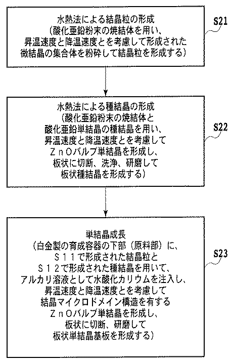
図5は、本発明に係る六方晶ウルツ鉱型化合物単結晶の製造方法の実施例2を説明するための工程図である。
水熱法による結晶粒の形成工程及び種結晶の形成工程については、上述した実施例1と同様である。つまり、まず、水熱法により、酸化亜鉛粉末の焼結体を用い、昇温速度と降温速度とを考慮して形成された微結晶の集合体を粉砕して結晶粒を形成する第1の工程(S21)と、次に、水熱法により、酸化亜鉛粉末の焼結体と酸化亜鉛単結晶の種結晶を用い、昇温速度と降温速度とを考慮して結晶マイクロドメイン構造を有するZnOバルク単結晶を形成してから板状種結晶を形成する第2の工程(S22)とを有する。
FIG. 5 is a process diagram for explaining Example 2 of the method for producing a hexagonal wurtzite compound single crystal according to the present invention.
The crystal grain formation step and seed crystal formation step by the hydrothermal method are the same as those in the first embodiment. That is, first, by using a sintered body of zinc oxide powder by a hydrothermal method, an aggregate of microcrystals formed in consideration of a temperature increase rate and a temperature decrease rate is pulverized to form crystal grains. Step (S21), and then, using a hydrothermal method, ZnO having a crystalline microdomain structure in consideration of the temperature increase rate and the temperature decrease rate, using a sintered body of zinc oxide powder and a seed crystal of zinc oxide single crystal A second step (S22) of forming a plate seed crystal after forming the bulk single crystal.
次に、本実施例2においては、上述した実施例1とは異なり、第1の工程で形成された結晶粒と、第2の工程で形成された板状種結晶を用い、アルカリ溶液として水酸化カリウムを使用し、昇温速度と降温速度とを考慮してZnOバルク単結晶を形成してから単結晶基板を形成する第3の工程(S23)を有している。 Next, in Example 2, unlike Example 1 described above, the crystal grains formed in the first step and the plate seed crystals formed in the second step are used, and water is used as an alkaline solution. A third step (S23) of forming a single crystal substrate after forming a ZnO bulk single crystal using potassium oxide in consideration of the rate of temperature rise and the rate of temperature fall is included.
上述した第3の工程(S23)においては、白金製の育成容器の下部(原料部)にアルカリ溶液として4.0mol/L水酸化カリウム溶液を250部を注入したこと以外は、実施例1と同様にしてZnOバルク単結晶を得た。この単結晶をc軸に垂直に厚さ0.8〜1.5mmの板状に切断し、研磨を実施して(0001)面の単結晶基板を得た。なお、成長中のオートクレーブ内力は1183気圧であった。 In the above-described third step (S23), Example 1 and Example 1 except that 250 parts of 4.0 mol / L potassium hydroxide solution was injected as an alkaline solution into the lower part (raw material part) of the platinum growth vessel. Similarly, a ZnO bulk single crystal was obtained. This single crystal was cut into a plate shape having a thickness of 0.8 to 1.5 mm perpendicular to the c-axis and polished to obtain a (0001) plane single crystal substrate. The growing autoclave internal force was 1183 atm.
得られた基板の特性評価を行った結果を表1に示す。 Table 1 shows the results of the characteristics evaluation of the obtained substrate.
実施例1、2で得られた単結晶基板上に、分子線エピタキシー装置を用いて以下の条件にて単結晶のZnO薄膜を成長した。まず、インコネル製の基板ホルダーに−c面が表面になるように単結晶基板を乗せて固定し、分子線エピタキシー装置内に導入した。 A single-crystal ZnO thin film was grown on the single-crystal substrates obtained in Examples 1 and 2 under the following conditions using a molecular beam epitaxy apparatus. First, a single crystal substrate was placed and fixed on an Inconel substrate holder so that the -c surface was the surface, and introduced into a molecular beam epitaxy apparatus.
これを真空中で基板温度が800℃になるまで加熱し、この状態で約10秒間維持することによって清浄な基板表面を得た。所望とする清浄な表面が得られたかどうかは、熱処理中に反射高速電子線回折パターンがストリーク状になることによって確認することが出来る。 This was heated in vacuum until the substrate temperature reached 800 ° C. and maintained in this state for about 10 seconds to obtain a clean substrate surface. Whether or not a desired clean surface has been obtained can be confirmed by the reflection high-energy electron diffraction pattern becoming streaky during the heat treatment.
次に、基板温度が500℃になるまで降温し、亜鉛と酸素を供給してZnO薄膜を成長した。典型的な成長条件として、亜鉛の分子線等価圧力は1.5×10⁻⁷Torr、酸素はRFプラズマソースを通して活性化した後、ラジカル状酸素を4.2×10⁻⁶Torrの圧力なるように供給した。成長した膜の膜厚は、成長時にマスクされていた部分との段差を測ることによって測定し、本実施例においては2時間の成長によって4000ÅのZnO薄膜を成長した。 Next, the temperature was lowered until the substrate temperature reached 500 ° C., and zinc and oxygen were supplied to grow a ZnO thin film. As typical growth conditions, the molecular beam equivalent pressure of zinc is 1.5 × 10 −7 Torr, oxygen is activated through an RF plasma source, and then radical oxygen is 4.2 × 10 −6 Torr. Supplied to. The film thickness of the grown film was measured by measuring the level difference from the masked part at the time of growth, and in this example, a 4000O ZnO thin film was grown by growth for 2 hours.
成長後の膜が良好な結晶性を有しているかどうかは、成長後の反射高速電子線回折パターンがストリーク状になるかどうかによって大まかに判断することが出来るが、断面TEMを観察することによって確認することが出来る。本実施例においても断面TEMを観察した結果、成長後の膜内に転位は全く観察されず、転位密度として少なくとも6×10⁻⁷cm-2以下であり、エピタキシャル成長用の基板として有用であることを確認した。 Whether or not the grown film has good crystallinity can be roughly determined by whether or not the reflected high-energy electron diffraction pattern after growth becomes streak-like, but by observing a cross-sectional TEM It can be confirmed. Also in this example, as a result of observing the cross-sectional TEM, no dislocation is observed in the grown film, and the dislocation density is at least 6 × 10 −7 cm −2 or less, which is useful as a substrate for epitaxial growth. It was confirmed.
(比較例1)
単結晶成長を実施する際の温度が、育成容器下部を383℃、上部を373℃としたこと以外は、実施例1と同様にしてZnOバルク単結晶、並びに(0001)面の単結晶基板を得た。得られた基板の特性評価を行った結果を表1に示す。
(Comparative Example 1)
The ZnO bulk single crystal and the (0001) plane single crystal substrate were formed in the same manner as in Example 1 except that the temperature during the single crystal growth was 383 ° C. for the lower portion of the growth vessel and 373 ° C. for the upper portion. Obtained. Table 1 shows the results of the characteristics evaluation of the obtained substrate.
(比較例2)
単結晶成長を実施する際の昇温速度が8℃/minとしたこと以外は、実施例1と同様にしてZnOバルク単結晶、並びに(0001)面の単結晶基板を得た。得られた基板の特性評価を行った結果を表1に示す。
(Comparative Example 2)
A ZnO bulk single crystal and a (0001) plane single crystal substrate were obtained in the same manner as in Example 1 except that the rate of temperature increase during the single crystal growth was 8 ° C./min. Table 1 shows the results of the characteristics evaluation of the obtained substrate.
(比較例3)
単結晶成長に用いる原料として、高純度科学社製高純度酸化亜鉛粉末より得られた粒度3mm〜10mmの焼結体を用いたこと以外は実施例1と同様にしてZnOバルク単結晶、並びに(0001)面の単結晶基板を得た。得られた基板の特性評価を行った結果を表1に示す。
(Comparative Example 3)
As a raw material used for single crystal growth, a ZnO bulk single crystal was used in the same manner as in Example 1 except that a sintered body having a particle size of 3 mm to 10 mm obtained from a high-purity zinc oxide powder manufactured by High-Purity Science Co., Ltd. was used. A 0001) plane single crystal substrate was obtained. Table 1 shows the results of the characteristics evaluation of the obtained substrate.
(比較例4)
市販(A社)のZnO単結晶基板を購入し、特性評価を行った。結果を表1に示す。
(Comparative Example 4)
A commercially available (Company A) ZnO single crystal substrate was purchased and evaluated. The results are shown in Table 1.
(比較例5)
市販(B社)のZnO単結晶基板を購入し、特性評価を行った。結果を表1に示す。
(Comparative Example 5)
A commercially available (Company B) ZnO single crystal substrate was purchased and evaluated. The results are shown in Table 1.
本発明は、転位欠陥が非常に低減され、かつ熱応力に強い六方晶ウルツ鉱型化合物単結晶及びそれより得られるエピタキシャル成長用単結晶基板を提供できる。そのため、基板上に薄膜を成膜した際の薄膜への悪影響が少なく、成膜からデバイス作動時における転位発生の顕著な低減を実現する、発光素子用の基板として好適である。 INDUSTRIAL APPLICABILITY The present invention can provide a hexagonal wurtzite compound single crystal having extremely reduced dislocation defects and being resistant to thermal stress, and a single crystal substrate for epitaxial growth obtained therefrom. Therefore, there is little adverse effect on the thin film when the thin film is formed on the substrate, and it is suitable as a substrate for a light-emitting element that realizes a remarkable reduction in dislocation generation from film formation during device operation.
11 酸化亜鉛単結晶育成装置
12 高圧用オートクレーブ
13 オートクレーブ収容部
14 オートクレーブ本体
15 パッキン部材
16 蓋体
17 ねじ
21,22 ヒータ
23 断熱材
31 酸化亜鉛単結晶育成容器
32 フレーム
33 支持具
34 内部バッフル板
35 バッフルリング
37 蓋
38 微少開口
41a乃至41d 種結晶
51 出発材料
DESCRIPTION OF
Claims (6)
連続、かつ一様な結晶格子を有するマトリックス領域内に、該マトリックス領域とは結晶格子の配列が異なる島状の結晶マイクロドメインを含み、該結晶マイクロドメイン内のc軸が、前記マトリックス領域のc軸と平行であり、
前記ウルツ鉱型化合物単結晶の任意の断面を透過型電子顕微鏡により観察倍率150万倍にて、70nm×40nmの領域で無作為に結晶格子像を20箇所観察したときに、前記マトリックス領域の中に前記マトリックス領域と結晶格子の方向性は同一であるが不連続である3〜50nmの大きさを持つ前記結晶マイクロドメインが存在し、該結晶マイクロドメインの面積の割合が、平均で観察箇所全体の50%以上あり、
前記ウルツ鉱型化合物単結晶が、ZnO,ZnMgO,ZnCdO,ZnCuO,ZnOS,ZnOSeから選ばれる材料であることを特徴とする六方晶系ウルツ鉱型化合物単結晶。 In a hexagonal wurtzite compound single crystal having an a-axis of 120 ° in a regular hexagonal plane and a c-axis perpendicular to the a-axis,
In a matrix region having a continuous and uniform crystal lattice, an island-like crystal microdomain having a different crystal lattice arrangement from the matrix region is included, and the c-axis in the crystal microdomain is c in the matrix region. Parallel to the axis,
When an arbitrary cross section of the wurtzite compound single crystal is observed at 20 crystal lattice images randomly in a 70 nm × 40 nm region with a transmission electron microscope at an observation magnification of 1.5 million, the inside of the matrix region is The crystal microdomain having a size of 3 to 50 nm that is discontinuous with the same direction of the matrix region and the crystal lattice exists, and the ratio of the area of the crystal microdomain is, on average, the entire observation location more than 50% of Ah is,
The wurtzite type compound single crystal, ZnO, ZnMgO, ZnCdO, ZnCuO , ZnOS, hexagonal wurtzite type compound single crystal, wherein a material der Rukoto selected from ZnOSe.
Priority Applications (1)
| Application Number | Priority Date | Filing Date | Title |
|---|---|---|---|
| JP2009049503A JP5510631B2 (en) | 2009-03-03 | 2009-03-03 | Hexagonal wurtzite compound single crystal and method for producing the same |
Applications Claiming Priority (1)
| Application Number | Priority Date | Filing Date | Title |
|---|---|---|---|
| JP2009049503A JP5510631B2 (en) | 2009-03-03 | 2009-03-03 | Hexagonal wurtzite compound single crystal and method for producing the same |
Publications (2)
| Publication Number | Publication Date |
|---|---|
| JP2010202454A JP2010202454A (en) | 2010-09-16 |
| JP5510631B2 true JP5510631B2 (en) | 2014-06-04 |
Family
ID=42964331
Family Applications (1)
| Application Number | Title | Priority Date | Filing Date |
|---|---|---|---|
| JP2009049503A Active JP5510631B2 (en) | 2009-03-03 | 2009-03-03 | Hexagonal wurtzite compound single crystal and method for producing the same |
Country Status (1)
| Country | Link |
|---|---|
| JP (1) | JP5510631B2 (en) |
Families Citing this family (2)
| Publication number | Priority date | Publication date | Assignee | Title |
|---|---|---|---|---|
| US8883556B2 (en) * | 2010-12-28 | 2014-11-11 | Semiconductor Energy Laboratory Co., Ltd. | Semiconductor device and manufacturing method thereof |
| CN114361443B (en) * | 2022-01-10 | 2024-06-04 | 宜宾锂宝新材料有限公司 | Single crystal ternary material, preparation method thereof and lithium battery |
Family Cites Families (1)
| Publication number | Priority date | Publication date | Assignee | Title |
|---|---|---|---|---|
| JP5519492B2 (en) * | 2008-04-26 | 2014-06-11 | 森 竜平 | Zinc oxide single crystal substrate manufacturing method, single crystal substrate grown by the method, and semiconductor light emitting device formed on the substrate |
-
2009
- 2009-03-03 JP JP2009049503A patent/JP5510631B2/en active Active
Also Published As
| Publication number | Publication date |
|---|---|
| JP2010202454A (en) | 2010-09-16 |
Similar Documents
| Publication | Publication Date | Title |
|---|---|---|
| US5530267A (en) | Article comprising heteroepitaxial III-V nitride semiconductor material on a substrate | |
| Yamane et al. | Preparation of GaN single crystals using a Na flux | |
| US9263266B2 (en) | Group III nitride articles and methods for making same | |
| KR100960834B1 (en) | Hexagonal urethane single crystal, method for manufacturing the same, and hexagonal urethane single crystal substrate | |
| US7829207B2 (en) | Manufacture method for ZnO based compound semiconductor crystal and ZnO based compound semiconductor substrate | |
| JP5638772B2 (en) | Method for growing zinc oxide based semiconductor and method for manufacturing semiconductor light emitting device | |
| WO2008047637A1 (en) | Process for producing nitride semiconductor, crystal growth rate enhancement agent, nitride single crystal, wafer and device | |
| Song et al. | Self-consistent growth of single-crystalline (2 [combining macron] 01) β-Ga 2 O 3 nanowires using a flexible GaN seed nanocrystal | |
| EP1790759A1 (en) | NITRIDE SEMICONDUCTOR SINGLE CRYSTAL INCLUDING Ga, METHOD FOR MANUFACTURING THE SAME, AND SUBSTRATE AND DEVICE USING THE CRYSTAL | |
| US20080191203A1 (en) | Method for Producing Gan Film, Semiconductor Device, Method for Generating Thin Film of Nitride of Group III Element and Semiconductor Device Having Thin Film of Nitride of Group III Element | |
| JP5870887B2 (en) | Annealing method of nitride single crystal | |
| Li et al. | Investigation of the crack extending downward along the seed of the β-Ga 2 O 3 crystal grown by the EFG method | |
| WO2012128263A1 (en) | Process for producing nitride crystal | |
| JP2017536325A (en) | Group III nitride crystals, methods for their production, and methods for producing bulk Group III nitride crystals in supercritical ammonia | |
| TWI404122B (en) | Method for enhancing growth of semi-polar (Al, In, Ga, B)N by metal organic chemical vapor deposition | |
| JP5510631B2 (en) | Hexagonal wurtzite compound single crystal and method for producing the same | |
| KR101810613B1 (en) | Hexagonal wurtzite single crystal | |
| Li et al. | Evolution of V-pits in the ammonothermal growth of GaN on HVPE-GaN seeds | |
| Aggarwal et al. | Semipolar r-plane ZnO films on Si (100) substrates: Thin film epitaxy and optical properties | |
| Li et al. | A new system for synthesis of high quality nonpolar GaN thin films | |
| Mahendran et al. | Characterization of manganese doped ZnO (MZO) thin films by spin coating technique | |
| EP2267193A1 (en) | Process for producing zno single crystal, self-supporting zno single-crystal wafer obtained by the same, self-supporting wafer of mg-containing zno mixed single crystal, and process for producing mg-containing zno mixed single crystal for use in the same | |
| Zhang et al. | Silica-controlled structure and optical properties of zinc oxide sol–gel thin films | |
| de Oliveira et al. | Identification of self-buffer layer on GaN/glass films grown by reactive sputtering | |
| Rusop et al. | Properties of zinc oxide thin films prepared on silicon (100) and glass substrates by pulsed laser deposition technique with different oxygen gas pressures |
Legal Events
| Date | Code | Title | Description |
|---|---|---|---|
| A621 | Written request for application examination |
Free format text: JAPANESE INTERMEDIATE CODE: A621 Effective date: 20120301 |
|
| A977 | Report on retrieval |
Free format text: JAPANESE INTERMEDIATE CODE: A971007 Effective date: 20130222 |
|
| A131 | Notification of reasons for refusal |
Free format text: JAPANESE INTERMEDIATE CODE: A131 Effective date: 20130301 |
|
| A521 | Written amendment |
Free format text: JAPANESE INTERMEDIATE CODE: A523 Effective date: 20130425 |
|
| A131 | Notification of reasons for refusal |
Free format text: JAPANESE INTERMEDIATE CODE: A131 Effective date: 20130607 |
|
| A521 | Written amendment |
Free format text: JAPANESE INTERMEDIATE CODE: A523 Effective date: 20130801 |
|
| TRDD | Decision of grant or rejection written | ||
| A01 | Written decision to grant a patent or to grant a registration (utility model) |
Free format text: JAPANESE INTERMEDIATE CODE: A01 Effective date: 20140225 |
|
| A61 | First payment of annual fees (during grant procedure) |
Free format text: JAPANESE INTERMEDIATE CODE: A61 Effective date: 20140311 |
|
| R150 | Certificate of patent or registration of utility model |
Ref document number: 5510631 Country of ref document: JP Free format text: JAPANESE INTERMEDIATE CODE: R150 |
|
| R250 | Receipt of annual fees |
Free format text: JAPANESE INTERMEDIATE CODE: R250 |
|
| R250 | Receipt of annual fees |
Free format text: JAPANESE INTERMEDIATE CODE: R250 |
|
| S531 | Written request for registration of change of domicile |
Free format text: JAPANESE INTERMEDIATE CODE: R313531 |
|
| R350 | Written notification of registration of transfer |
Free format text: JAPANESE INTERMEDIATE CODE: R350 |
|
| R250 | Receipt of annual fees |
Free format text: JAPANESE INTERMEDIATE CODE: R250 |
|
| R250 | Receipt of annual fees |
Free format text: JAPANESE INTERMEDIATE CODE: R250 |