JP5505915B1 - Communication module - Google Patents
Communication module Download PDFInfo
- Publication number
- JP5505915B1 JP5505915B1 JP2013236650A JP2013236650A JP5505915B1 JP 5505915 B1 JP5505915 B1 JP 5505915B1 JP 2013236650 A JP2013236650 A JP 2013236650A JP 2013236650 A JP2013236650 A JP 2013236650A JP 5505915 B1 JP5505915 B1 JP 5505915B1
- Authority
- JP
- Japan
- Prior art keywords
- processing unit
- unit
- circuit board
- power supply
- frequency
- Prior art date
- Legal status (The legal status is an assumption and is not a legal conclusion. Google has not performed a legal analysis and makes no representation as to the accuracy of the status listed.)
- Expired - Fee Related
Links
Images


Classifications
-
- H—ELECTRICITY
- H04—ELECTRIC COMMUNICATION TECHNIQUE
- H04B—TRANSMISSION
- H04B15/00—Suppression or limitation of noise or interference
- H04B15/02—Reducing interference from electric apparatus by means located at or near the interfering apparatus
- H04B15/04—Reducing interference from electric apparatus by means located at or near the interfering apparatus the interference being caused by substantially sinusoidal oscillations, e.g. in a receiver or in a tape-recorder
-
- H—ELECTRICITY
- H04—ELECTRIC COMMUNICATION TECHNIQUE
- H04B—TRANSMISSION
- H04B1/00—Details of transmission systems, not covered by a single one of groups H04B3/00 - H04B13/00; Details of transmission systems not characterised by the medium used for transmission
- H04B1/38—Transceivers, i.e. devices in which transmitter and receiver form a structural unit and in which at least one part is used for functions of transmitting and receiving
- H04B1/3827—Portable transceivers
- H04B1/3888—Arrangements for carrying or protecting transceivers
-
- H—ELECTRICITY
- H05—ELECTRIC TECHNIQUES NOT OTHERWISE PROVIDED FOR
- H05K—PRINTED CIRCUITS; CASINGS OR CONSTRUCTIONAL DETAILS OF ELECTRIC APPARATUS; MANUFACTURE OF ASSEMBLAGES OF ELECTRICAL COMPONENTS
- H05K1/00—Printed circuits
- H05K1/02—Details
- H05K1/0213—Electrical arrangements not otherwise provided for
- H05K1/0216—Reduction of cross-talk, noise or electromagnetic interference
- H05K1/0218—Reduction of cross-talk, noise or electromagnetic interference by printed shielding conductors, ground planes or power plane
-
- H—ELECTRICITY
- H01—ELECTRIC ELEMENTS
- H01L—SEMICONDUCTOR DEVICES NOT COVERED BY CLASS H10
- H01L2224/00—Indexing scheme for arrangements for connecting or disconnecting semiconductor or solid-state bodies and methods related thereto as covered by H01L24/00
- H01L2224/01—Means for bonding being attached to, or being formed on, the surface to be connected, e.g. chip-to-package, die-attach, "first-level" interconnects; Manufacturing methods related thereto
- H01L2224/10—Bump connectors; Manufacturing methods related thereto
- H01L2224/15—Structure, shape, material or disposition of the bump connectors after the connecting process
- H01L2224/16—Structure, shape, material or disposition of the bump connectors after the connecting process of an individual bump connector
- H01L2224/161—Disposition
- H01L2224/16151—Disposition the bump connector connecting between a semiconductor or solid-state body and an item not being a semiconductor or solid-state body, e.g. chip-to-substrate, chip-to-passive
- H01L2224/16221—Disposition the bump connector connecting between a semiconductor or solid-state body and an item not being a semiconductor or solid-state body, e.g. chip-to-substrate, chip-to-passive the body and the item being stacked
- H01L2224/16225—Disposition the bump connector connecting between a semiconductor or solid-state body and an item not being a semiconductor or solid-state body, e.g. chip-to-substrate, chip-to-passive the body and the item being stacked the item being non-metallic, e.g. insulating substrate with or without metallisation
- H01L2224/16227—Disposition the bump connector connecting between a semiconductor or solid-state body and an item not being a semiconductor or solid-state body, e.g. chip-to-substrate, chip-to-passive the body and the item being stacked the item being non-metallic, e.g. insulating substrate with or without metallisation the bump connector connecting to a bond pad of the item
-
- H—ELECTRICITY
- H01—ELECTRIC ELEMENTS
- H01L—SEMICONDUCTOR DEVICES NOT COVERED BY CLASS H10
- H01L2924/00—Indexing scheme for arrangements or methods for connecting or disconnecting semiconductor or solid-state bodies as covered by H01L24/00
- H01L2924/0001—Technical content checked by a classifier
- H01L2924/0002—Not covered by any one of groups H01L24/00, H01L24/00 and H01L2224/00
-
- H—ELECTRICITY
- H01—ELECTRIC ELEMENTS
- H01L—SEMICONDUCTOR DEVICES NOT COVERED BY CLASS H10
- H01L2924/00—Indexing scheme for arrangements or methods for connecting or disconnecting semiconductor or solid-state bodies as covered by H01L24/00
- H01L2924/30—Technical effects
- H01L2924/301—Electrical effects
- H01L2924/3025—Electromagnetic shielding
-
- H—ELECTRICITY
- H05—ELECTRIC TECHNIQUES NOT OTHERWISE PROVIDED FOR
- H05K—PRINTED CIRCUITS; CASINGS OR CONSTRUCTIONAL DETAILS OF ELECTRIC APPARATUS; MANUFACTURE OF ASSEMBLAGES OF ELECTRICAL COMPONENTS
- H05K2201/00—Indexing scheme relating to printed circuits covered by H05K1/00
- H05K2201/07—Electric details
- H05K2201/0707—Shielding
- H05K2201/0715—Shielding provided by an outer layer of PCB
-
- H—ELECTRICITY
- H05—ELECTRIC TECHNIQUES NOT OTHERWISE PROVIDED FOR
- H05K—PRINTED CIRCUITS; CASINGS OR CONSTRUCTIONAL DETAILS OF ELECTRIC APPARATUS; MANUFACTURE OF ASSEMBLAGES OF ELECTRICAL COMPONENTS
- H05K2201/00—Indexing scheme relating to printed circuits covered by H05K1/00
- H05K2201/10—Details of components or other objects attached to or integrated in a printed circuit board
- H05K2201/10227—Other objects, e.g. metallic pieces
- H05K2201/10371—Shields or metal cases
-
- H—ELECTRICITY
- H05—ELECTRIC TECHNIQUES NOT OTHERWISE PROVIDED FOR
- H05K—PRINTED CIRCUITS; CASINGS OR CONSTRUCTIONAL DETAILS OF ELECTRIC APPARATUS; MANUFACTURE OF ASSEMBLAGES OF ELECTRICAL COMPONENTS
- H05K3/00—Apparatus or processes for manufacturing printed circuits
- H05K3/22—Secondary treatment of printed circuits
- H05K3/28—Applying non-metallic protective coatings
- H05K3/284—Applying non-metallic protective coatings for encapsulating mounted components
Landscapes
- Engineering & Computer Science (AREA)
- Signal Processing (AREA)
- Computer Networks & Wireless Communication (AREA)
- Physics & Mathematics (AREA)
- Electromagnetism (AREA)
- Microelectronics & Electronic Packaging (AREA)
- Transceivers (AREA)
- Non-Metallic Protective Coatings For Printed Circuits (AREA)
- Shielding Devices Or Components To Electric Or Magnetic Fields (AREA)
- Production Of Multi-Layered Print Wiring Board (AREA)
- Structures Or Materials For Encapsulating Or Coating Semiconductor Devices Or Solid State Devices (AREA)
Abstract
【課題】高機能且つ小型化な携帯電話用の通信モジュールを提供する。
【解決手段】通信モジュール100は、携帯電話通信に係る第1高周波処理部610と、ベースバンド処理部及びアプリケーション処理部を有するシステム部630と、電源回路部640とが実装された回路基板800と、回路基板800に実装された電子部品を被覆する封止部材900と、封止部材900の表面に形成された導電性のシールド層901と、前記システム部630及び電源回路部640の何れか一方又は双方の実装領域と前記第1高周波処理部610の実装領域とを区画するように封止部材900に形成したシールド壁902とを備えた。前記回路基板800は、他の導体層より厚みが大きく且つグランドとして機能する導体層であるコア層810を備えた。コア層810に形成された貫通孔811には電子部品が配置されている。
【選択図】図2A communication module for a mobile phone having high functionality and a small size is provided.
A communication module includes a first high frequency processing unit 610 related to mobile phone communication, a system unit 630 having a baseband processing unit and an application processing unit, and a circuit board 800 on which a power supply circuit unit 640 is mounted. The sealing member 900 that covers the electronic component mounted on the circuit board 800, the conductive shield layer 901 formed on the surface of the sealing member 900, and any one of the system unit 630 and the power supply circuit unit 640 Alternatively, a shield wall 902 formed on the sealing member 900 is provided so as to partition both mounting regions and the mounting region of the first high-frequency processing unit 610. The circuit board 800 includes a core layer 810 that is a conductor layer that is thicker than other conductor layers and functions as a ground. Electronic components are arranged in the through holes 811 formed in the core layer 810.
[Selection] Figure 2
Description
本発明は、携帯電話で用いられる通信モジュールに関する。 The present invention relates to a communication module used in a mobile phone.
近年、所謂スマートフォンと呼ばれる多機能携帯電話に代表されるように携帯電話の多機能化及び小型化が図られている。このような携帯電話としては、高周波信号の送受信に必要な各種フロントエンド部品を回路基板に集約実装した高周波回路モジュールを、マザーボードに搭載したものが知られている(例えば特許文献1参照)。ここでフロントエンド部品とは、高周波信号を処理する高周波ICとアンテナとの間の経路上に配置される高周波信号処理用の受動部品や能動部品を意味する。特許文献1に記載の高周波回路モジュールでは、回路基板上に電力増幅用IC、送信フィルタ、受信フィルタ等のフロントエンド部品が搭載されている。また回路基板内には整合回路などを構成するキャパシタなどの受動部品が埋設されている。特許文献1に記載の高周波回路モジュールは、セルラー方式800MHz帯及びPCS(Personal Communication Services)方式1.9GHz帯の周波数帯域を持った2つの送受信系と、GPS(Global Positioning System)による測位機能を利用するためGPSの受信バンド1.5GHz帯を持った1つの受信系とを備えている。
In recent years, as represented by a multi-function mobile phone called a so-called smart phone, the multi-function and miniaturization of the mobile phone have been attempted. As such a cellular phone, there is known a mobile phone in which a high-frequency circuit module in which various front-end components necessary for transmitting and receiving a high-frequency signal are collectively mounted on a circuit board is mounted on a motherboard (for example, see Patent Document 1). Here, the front end component means a passive component or an active component for high-frequency signal processing arranged on a path between a high-frequency IC that processes a high-frequency signal and the antenna. In the high-frequency circuit module described in Patent Document 1, front-end components such as a power amplification IC, a transmission filter, and a reception filter are mounted on a circuit board. In addition, passive components such as capacitors constituting a matching circuit and the like are embedded in the circuit board. The high-frequency circuit module described in Patent Literature 1 uses two transmission / reception systems having a frequency band of a
特許文献1に記載の高周波回路モジュールではフロントエンド部品のみを集約しているが、近年では更なる高密度化・高機能化を実現すべく、フロントエンド部品だけでなく、高周波IC、更には電源回路やベースバンド信号の処理回路やメモリなど携帯電話のほぼ全ての機能を1つの回路基板に集約したいという要望がある。しかし、特許文献1に記載の高周波回路モジュールに、ベースバンド処理回路やメモリや電源回路を実装するとともに全体サイズを小型化しようとすると、(a)各機能部が接近しているので各機能部間でノイズが混入して特性劣化が生じやすい、(b)各機能部が接近しているので放熱効率が低下する、(c)小型化した場合であっても従前の高周波回路モジュールと比較すれば回路基板サイズが大きいため実装時などで反りが生じやすい、という問題があった。 In the high-frequency circuit module described in Patent Document 1, only front-end components are integrated, but in recent years, not only front-end components but also high-frequency ICs and power supplies have been developed in order to achieve higher density and higher functionality. There is a desire to consolidate almost all functions of a mobile phone such as a circuit, a baseband signal processing circuit, and a memory on a single circuit board. However, when a baseband processing circuit, a memory, or a power supply circuit is mounted on the high-frequency circuit module described in Patent Document 1 and an attempt is made to reduce the overall size, (a) since each functional unit is close, (B) The heat radiation efficiency is reduced because the functional units are close to each other, and (c) even when downsized, compared to the conventional high-frequency circuit module. If the circuit board size is large, there is a problem that warpage is likely to occur during mounting.
なお、前記(a)の課題について、この種の製品では電源回路として高周波回路用の電源回路とその他の回路用の電源回路とを備えており、特に小型化のため各電源回路はスイッチングレギュレータ方式を採用している。このため、他の回路用の電源回路で生じたスイッチングノイズが高周波回路用の電源回路と電磁結合し、その結果、スイッチングノイズが高周波回路に伝搬して高周波特性の劣化を招く場合がある。または、電源回路で生じたスイッチングノイズが直接高周波回路に電磁結合することにより高周波特性の劣化を招く場合もある。 As for the problem (a), this type of product includes a power supply circuit for a high-frequency circuit and a power supply circuit for other circuits as a power supply circuit. Is adopted. For this reason, switching noise generated in the power supply circuit for other circuits is electromagnetically coupled to the power supply circuit for the high frequency circuit, and as a result, the switching noise may propagate to the high frequency circuit and cause deterioration of the high frequency characteristics. Alternatively, the switching noise generated in the power supply circuit may be electromagnetically coupled directly to the high-frequency circuit, thereby deteriorating the high-frequency characteristics.
本発明は、上記事情に鑑みてなされたものであり、その目的とするところは、高機能且つ小型化な携帯電話用の通信モジュールを提供することにある。 The present invention has been made in view of the above circumstances, and an object of the present invention is to provide a highly functional and compact communication module for a mobile phone.
上記目的を達成するために、本願発明に係る通信モジュールは、(a)携帯電話通信に係る高周波信号を処理する第1高周波処理部、(b)携帯電話通信に係るベースバンド信号を処理するベースバンド処理部及び携帯電話の各種アプリケーション動作を処理するアプリケーション処理部を有するシステム部、(c)電源回路部が実装された回路基板と、
回路基板の一方の主面の全面に亘って形成され該主面に実装された電子部品を被覆する封止部材と、封止部材の表面に形成された導電性のシールド層と、前記システム部及び電源回路部の何れか一方又は双方の実装領域と前記第1高周波処理部の実装領域とを区画するように封止部材の主面から回路基板の一方の主面側に向かって形成された溝部を充填し且つ前記シールド層と導通した第1シールド壁とを備え、前記電源回路部は第1高周波処理部用の第1電源回路部とシステム部用の第2電源回路部とを含み、第1電源回路部の実装領域と第2電源回路部の実装領域とを区画するように封止部材の主面から回路基板の一方の主面側に向かって形成された溝部を充填し且つ前記シールド層と導通した第2シールド壁とを備えたことを特徴とする。
In order to achieve the above object, a communication module according to the present invention includes: (a) a first high-frequency processing unit that processes a high-frequency signal related to mobile phone communication; and (b) a base that processes a baseband signal related to mobile phone communication. A system unit having an application processing unit for processing various application operations of a band processing unit and a mobile phone; (c) a circuit board on which a power supply circuit unit is mounted;
A sealing member formed over the entire surface of one main surface of the circuit board and covering an electronic component mounted on the main surface; a conductive shield layer formed on the surface of the sealing member; and the system unit And the power supply circuit unit is formed from the main surface of the sealing member toward one main surface side of the circuit board so as to partition the mounting region of one or both of the power supply circuit unit and the mounting region of the first high-frequency processing unit. A first shield wall filling the groove and electrically connected to the shield layer, wherein the power supply circuit unit includes a first power supply circuit unit for the first high-frequency processing unit and a second power supply circuit unit for the system unit; Filling a groove formed from the main surface of the sealing member toward one main surface side of the circuit board so as to partition the mounting region of the first power circuit unit and the mounting region of the second power circuit unit; It is characterized in that a second shielding wall is conducted to the shield layer .
本発明によれば、携帯電話の構成に必要な主要機能部の多くが1つのモジュールに集約されているので高機能且つ小型化が図られる。ここで本発明では、部品実装面である回路基板の一方の主面に形成された封止部材に、システム部及び電源回路部の何れか一方又は双方の実装領域と第1高周波処理部の実装領域とを区画するように溝部が形成されており、且つ、該溝部には第1シールド壁が充填されている。これによりシステム部及び電源回路部から第1高周波処理部へのノイズの侵入を防止できるので高周波特性に優れたものとなる。また本発明によれば、第2電源回路部で生じたノイズが第1電源回路部を介して第1高周波処理部に伝搬することを第2シールド壁により防止できるので、高周波回路の特性劣化をさらに効果的に防止できる。また本発明では、回路基板の一方の主面に全面に亘って電子部品を被覆する封止材料が形成されているので、該封止部材によっても高い放熱効率が得られるとともに、適切な封止部材を選択することにより回路基板の反りを抑えることができる。以上のように本発明に係る通信モジュールは、携帯電話の構成に必要な主要機能部の多くが集約されているにもかかわらず、高周波回路の特性劣化を防止でき、放熱効率が高く、反りが生じにくいものとなる。 According to the present invention, since many of the main functional units necessary for the configuration of the mobile phone are concentrated in one module, high functionality and downsizing can be achieved. Here, in the present invention, the sealing member formed on one main surface of the circuit board, which is a component mounting surface, is mounted with one or both of the mounting region of the system unit and the power circuit unit and the first high-frequency processing unit. A groove is formed so as to partition the region, and the first shield wall is filled in the groove. As a result, noise can be prevented from entering from the system unit and the power supply circuit unit to the first high frequency processing unit, so that the high frequency characteristics are excellent. Further, according to the present invention, the noise generated in the second power supply circuit unit can be prevented from propagating to the first high frequency processing unit via the first power supply circuit unit by the second shield wall. Furthermore, it can be effectively prevented. In the present invention, since the sealing material covering the electronic component on the entire surface on one main surface of the circuit board is formed, together with the resulting higher heat dissipation efficiency by sealing member, suitable sealing The warping of the circuit board can be suppressed by selecting the member. Communication module according to the present invention as the following are a number of main functional unit required to configure the mobile phone Despite the intensive, can prevent deterioration of the characteristics of the high-frequency circuit, the heat radiation efficiency is high, warping Is unlikely to occur.
また、本願発明に係る通信モジュールは、(a)携帯電話通信に係る高周波信号を処理する第1高周波処理部、(b)携帯電話通信に係るベースバンド信号を処理するベースバンド処理部及び携帯電話の各種アプリケーション動作を処理するアプリケーション処理部を有するシステム部、(c)電源回路部が実装された回路基板と、回路基板の一方の主面の全面に亘って形成され該主面に実装された電子部品を被覆する封止部材と、封止部材の表面に形成された導電性のシールド層と、前記システム部及び電源回路部の何れか一方又は双方の実装領域と前記第1高周波処理部の実装領域とを区画するように封止部材の主面から回路基板の一方の主面側に向かって形成された溝部を充填し且つ前記シールド層と導通した第1シールド壁と、前記回路基板に実装され非携帯電話通信に係る高周波信号を処理する第2高周波処理部と、前記システム部及び電源回路部の何れか一方又は双方の実装領域と前記第2高周波処理部の実装領域とを区画するように封止部材の主面から回路基板の一方の主面側に向かって形成された溝部を充填し且つ前記シールド層と導通した第3シールド壁とを備えたことを特徴とする。 The communication module according to the present invention includes (a) a first high-frequency processing unit that processes a high-frequency signal related to mobile phone communication, (b) a baseband processing unit that processes a baseband signal related to mobile phone communication, and a mobile phone. A system unit having an application processing unit for processing various application operations, (c) a circuit board on which a power supply circuit unit is mounted, and one main surface of the circuit board, and is mounted on the main surface A sealing member that covers the electronic component, a conductive shield layer formed on the surface of the sealing member, a mounting region of one or both of the system unit and the power supply circuit unit, and the first high-frequency processing unit. a first shield wall is conducted to and filling the grooves formed toward the one main surface side of the circuit board the shielding layer from the main surface of the sealing member so as to define a mounting region, wherein A second high-frequency processing unit that is mounted on the road board and processes a high-frequency signal related to non-mobile phone communication; a mounting region of one or both of the system unit and the power supply circuit unit; and a mounting region of the second high-frequency processing unit And a third shield wall filled with a groove formed from the main surface of the sealing member toward one main surface of the circuit board so as to partition the shield member. The
本発明によれば、携帯電話の構成に必要な主要機能部の多くが1つのモジュールに集約されているので高機能且つ小型化が図られる。ここで本発明では、部品実装面である回路基板の一方の主面に形成された封止部材に、システム部及び電源回路部の何れか一方又は双方の実装領域と第1高周波処理部の実装領域とを区画するように溝部が形成されており、且つ、該溝部には第1シールド壁が充填されている。これによりシステム部及び電源回路部から第1高周波処理部へのノイズの侵入を防止できるので高周波特性に優れたものとなる。また本発明によれば、システム部及び電源回路部から第2高周波処理部へのノイズの侵入を第3シールド壁により防止できるので高周波特性に優れたものとなる。また本発明では、回路基板の一方の主面に全面に亘って電子部品を被覆する封止材料が形成されているので、該封止部材によっても高い放熱効率が得られるとともに、適切な封止部材を選択することにより回路基板の反りを抑えることができる。以上のように本発明に係る通信モジュールは、携帯電話の構成に必要な主要機能部の多くが集約されているにもかかわらず、高周波回路の特性劣化を防止でき、放熱効率が高く、反りが生じにくいものとなる。 According to the present invention, since many of the main functional units necessary for the configuration of the mobile phone are concentrated in one module, high functionality and downsizing can be achieved. Here, in the present invention, the sealing member formed on one main surface of the circuit board, which is a component mounting surface, is mounted with one or both of the mounting region of the system unit and the power circuit unit and the first high-frequency processing unit. A groove is formed so as to partition the region, and the first shield wall is filled in the groove. As a result, noise can be prevented from entering from the system unit and the power supply circuit unit to the first high frequency processing unit, so that the high frequency characteristics are excellent. Further , according to the present invention, noise can be prevented from entering from the system unit and the power supply circuit unit to the second high-frequency processing unit by the third shield wall, so that the high-frequency characteristics are excellent. In the present invention, since the sealing material for covering the electronic component is formed over the entire main surface of one of the circuit boards, the sealing member can provide high heat radiation efficiency and can be appropriately sealed. The warping of the circuit board can be suppressed by selecting the member. As described above, the communication module according to the present invention can prevent deterioration of the characteristics of the high-frequency circuit, has high heat dissipation efficiency, and is warped despite the fact that many of the main functional units necessary for the configuration of the mobile phone are concentrated. It is difficult to occur.
また本発明の好適な態様の一例としては、前記第1高周波処理部の実装領域と第2高周波処理部の実装領域との間にシステム部の実装領域が配置されていることを特徴とするものが挙げられる。 As an example of a preferred aspect of the present invention, a mounting area for the system unit is disposed between the mounting area for the first high-frequency processing unit and the mounting area for the second high-frequency processing unit. Is mentioned.
一般的に携帯電話通信で用いられるアンテナと、例えば衛星測位システムなど非携帯電話通信で用いられるアンテナとは、両者間の干渉を防止するために携帯電話の筐体内においてできるだけ距離をおいて実装される。本発明では、携帯電話通信に係る第1高周波処理部の実装領域と非携帯電話通信に係る第2高周波処理部の実装領域との間にシステム部の実装領域が介在するので、必然的に、第1高周波処理部の実装領域と第2高周波処理部の実装領域との距離が大きくなる。これにより、前述したようなアンテナ実装を容易に実現できるのとともに、各アンテナと高周波回路部との配線長を短くできるので高周波特性にも優れたものとなる。In general, an antenna used for mobile phone communication and an antenna used for non-mobile phone communication such as a satellite positioning system are mounted as far as possible in the case of the mobile phone to prevent interference between them. The In the present invention, since the mounting region of the system unit is interposed between the mounting region of the first high-frequency processing unit related to mobile phone communication and the mounting region of the second high-frequency processing unit related to non-mobile phone communication, inevitably, The distance between the mounting region of the first high-frequency processing unit and the mounting region of the second high-frequency processing unit is increased. As a result, the antenna mounting as described above can be easily realized, and the wiring length between each antenna and the high-frequency circuit unit can be shortened, so that the high-frequency characteristics are excellent.
また本発明の好適な態様の一例としては、前記回路基板は、導体層と絶縁体層とを積層してなるとともに、他の導体層より厚みが大きく且つグランドとして機能する導体層であるコア層を備え、前記第1高周波処理部・システム部・電源回路部のうちの少なくとも何れか1つを構成する1つ以上の電子部品は前記回路基板のコア層に形成された貫通孔又は凹部内に配置されていることを特徴とするものが挙げられる。As an example of a preferred aspect of the present invention, the circuit board is a core layer that is a conductor layer that is formed by laminating a conductor layer and an insulator layer, and is thicker than other conductor layers and functions as a ground. And at least one electronic component constituting at least one of the first high-frequency processing unit, the system unit, and the power supply circuit unit is in a through hole or a recess formed in the core layer of the circuit board. The thing characterized by being arrange | positioned is mentioned.
本発明によれば、回路基板がグランドとして機能するコア層を備えており、該コア層に形成された貫通孔又は凹部に電子部品が配置されているので、高密度化が図られるとともに埋設された電子部品は高いシールド性を有するものとなる。また本発明では、回路基板がコア層を備えているので各機能部で発生した熱がコア層に伝導し、さらに該コア層において面方向に拡散する。これにより高い放熱効率が得られる。さらに本発明では、回路基板がコア層を備えているので回路基板は反りが生じにくく、さらに適切な封止部材を選択することにより回路基板の反りを抑えることができる。According to the present invention, the circuit board includes a core layer that functions as a ground, and the electronic component is disposed in the through hole or the recess formed in the core layer, so that the density is increased and the circuit board is embedded. The electronic parts have high shielding properties. In the present invention, since the circuit board includes the core layer, heat generated in each functional unit is conducted to the core layer and further diffuses in the plane direction in the core layer. Thereby, high heat dissipation efficiency is obtained. Furthermore, in the present invention, since the circuit board is provided with the core layer, the circuit board is hardly warped, and the warpage of the circuit board can be suppressed by selecting an appropriate sealing member.
以上説明したように本発明に係る通信モジュールは、携帯電話の構成に必要な主要機能部の多くが集約されているにもかかわらず、高周波回路の特性劣化を防止でき、放熱効率が高く、反りが生じにくいものとなる。 As described above, the communication module according to the present invention can prevent deterioration of the characteristics of the high-frequency circuit, has high heat dissipation efficiency, and is warped despite the fact that many of the main functional units necessary for the configuration of the mobile phone are concentrated. Is unlikely to occur.
本発明の一実施の形態に係る通信モジュールについて図面を参照して説明する。図1は通信モジュールの概略ブロック図である。なお本実施の形態では、説明の簡単のため、主として本発明の要旨に係る構成について説明する。 A communication module according to an embodiment of the present invention will be described with reference to the drawings. FIG. 1 is a schematic block diagram of a communication module. In the present embodiment, for simplicity of explanation, a configuration according to the gist of the present invention will be mainly described.
本実施の形態に係る通信モジュール100は、いわゆるスマートフォンと呼ばれる多機能携帯電話の主要機能を1つのモジュールとして集約したものである。具体的には、通信モジュール100は、広域の無線通信網である携帯電話網の通信通話機能、近距離の無線通信であるWiFi(登録商標)やBluetooth(登録商標)の機能、衛星測位システムの1つであるGPS機能等を備えている。なお本実施の形態に係る本通信モジュール100は、説明の簡単のため、2つの周波数帯域のW−CDMA(Wideband Code Division Multiple Access)及びLTE(Long Term Evolution)並びに2つの周波数帯域のGSM(Global System for Mobile communications)に対応するものとする。
The
図1に示すように、通信モジュール100は、携帯電話網用の送受信回路を備えている。具体的には、通信モジュール100は、フロントエンド部品として、高周波スイッチ101と、第1及び第2デュプレクサ110,120と、高周波電力増幅器131,132と、第1バンドパスフィルタ140を備えている。また通信モジュール100は、RFIC(Radio Frequency Integrated Circuit)190を備えている。該RFIC190は、後述するように、携帯電話通信に係る高周波信号の処理だけでなく、GPS受信信号の処理も行う。RFIC190は、携帯電話通信に係る高周波信号の受信回路及び送信回路を備えるとともに高周波信号の変復調処理などを行う。
As shown in FIG. 1, the
また通信モジュール100は、GPS用のフロントエンド部品として、ダイプレクサ310、第2バンドパスフィルタ320、低雑音増幅器330、第3バンドパスフィルタ340を備えている。さらにWiFi用のフロントエンド部品として、第4バンドパスフィルタ350を備えている。なお、図1からも明らかなように、前記ダイプレクサ310はWiFi及びBluetooth用のフロントエンド部品でもある。また、通信モジュール100は、WiFi通信用のRFIC390を備えている。
The
また通信モジュール100は、各通信に係るデジタル信号の処理機能(所謂ベースバンド機能)や、その他各種携帯電話のアプリケーション機能(例えばカメラの制御や撮像データの処理など)を担う中央演算装置であるベースバンドIC400と、メモリ410とを備えている。
The
なお通信モジュール100は、上述の回路部品の他、後述する電源回路、デジタル処理の基準となるクロック回路等を備えているが、図1では説明を省略する。また、通信モジュール100は、他の高周波信号処理の主要部品としてダイバーシティ受信回路や2系統同時通信用の送受信回路を構成するためのフロントエンド部品やRFICを備えていてもよい。
The
高周波スイッチ101は、2つの内蔵スイッチ102及び103と、2つの高周波電力増幅器105及び106を1つのパッケージに集約したものである。内蔵スイッチ102は、第1又は第2デュプレクサ110,120、第1バンドパスフィルタ140、高周波電力増幅器105,106と1つの外部アンテナ11との接続を切り替える。内蔵スイッチ103は、2つの高周波電力増幅器105,106とRFIC190との接続を切り替える。高周波電力増幅器105は、GSMの周波数区分のうち1GHz以上の送信信号を増幅する。高周波電力増幅器106は、GSMの周波数区分のうち1GHz未満の送信信号を増幅する。内蔵スイッチ103は、RFIC190のGSM用の送信ポートに接続している。該送信ポートは、GSMの900MHz帯及び1900MHz帯で共通となっている。
The
各デュプレクサ110,120は、それぞれ送信フィルタ112,122と受信フィルタ114,124とを備えている。送信フィルタ112,122及び受信フィルタ114,124としては、表面弾性波(SAW:Surface Acoustic Wave)フィルタやバルク弾性波(BAW:Bulk Acoustic Wave)フィルタなどの弾性波フィルタなど種々のものを用いることができる。本実施の形態では、各フィルタとしてSAWフィルタを用いた。また本実施の形態では、各デュプレクサ110,120は、それぞれ送信フィルタ112,122と受信フィルタ114,124とを1つのパッケージに収容したものを用いた。
Each of the
各送信フィルタ112,122は高周波電力増幅器131,132を介してRFIC190のW−CDMA及びLTE用の送信ポートに接続している。各受信フィルタ114,124はRFIC190の受信ポートに接続している。なお本実施の形態では、受信フィルタ114はW−CDMA及びLTE用の受信ポートに接続しており、受信フィルタ124はW−CDMA及びLTE並びにGSM用の受信ポートに接続している。本実施の形態では、高周波電力増幅器131,132は、パワーアンプIC139として1つのパッケージに集積されている。また、第1バンドパスフィルタ140はRFIC190のGSM用の受信ポートに接続している。第1バンドパスフィルタ140としては、SAWフィルタやBAWフィルタなどの弾性波フィルタなど種々のものを用いることができる。本実施の形態では、当該フィルタとしてSAWフィルタを用いた。
The transmission filters 112 and 122 are connected to the W-CDMA and LTE transmission ports of the
前述のように本実施の形態に係る通信モジュール100は、2つのW−CDMA及びLTE並びに2つのGSMに対応しており、デュプレクサ110,120及びバンドパスフィルタ140は各周波数帯域の高周波信号のみが通過するようフィルタリングする。
As described above, the
具体的には、第1デュプレクサ110は、2100MHz帯のW−CDMA(Wideband Code Division Multiple Access)又はLTE(Long Term Evolution)に対応している。したがって、第1送信フィルタ112は1920〜1980MHzのバンドパスフィルタであり、第1受信フィルタ114は2110〜2170MHzのバンドパスフィルタである。一方、第2デュプレクサ120は、900MHz帯のW−CDMA又はLTE並びにGSMに対応している。したがって、第2送信フィルタ122は880〜915MHzのバンドパスフィルタであり、第2受信フィルタ124は925〜960MHzのバンドパスフィルタである。
Specifically, the
また、第1バンドパスフィルタ140は、1900MHz帯のGSMにおいて受信信号を濾過するためのフィルタであり、1930〜1990MHz帯のバンドパスフィルタである。
The
前記ダイプレクサ310は、アンテナ20で送受信する高周波信号を、GPS受信信号とWiFi通信に係る高周波信号とに分波するための素子であり、GPS受信信号のみを通過させるバンドパスフィルタ312とWiFi通信に係る高周波信号のみを通過させるバンドパスフィルタ311とを備えている。本実施の形態では、ダイプレクサ310は、各バンドパスフィルタ311,312を1つのパッケージに収容したものを用いた。なお、ダイプレクサ310は、GPS受信信号を通過させるとともにWiFi通信に係る高周波信号を通過させないローパスフィルタと、WiFi通信に係る高周波信号を通過させるとともにGPS受信信号を通過させないハイパスフィルタとにより構成するようにしてもよい。
The
第2バンドパスフィルタ320及び第3バンドパスフィルタ340は、それぞれGPS受信信号のみを通過させるフィルタである。各バンドパスフィルタ320,340としては、SAWフィルタやBAWフィルタなどの弾性波フィルタなど種々のものを用いることができる。本実施の形態では、各フィルタとしてSAWフィルタを用いた。第3バンドパスフィルタ340は、前記RFIC190の受信ポートに接続している。本実施の形態において、GPS用のフロントエンド部品が前述したような構成となっている理由は、GPS受信信号が微弱であること及び後述するようにアンテナ20と接続するための端子とRFIC190との距離が大きく離れていることから、低損失の第2バンドバスフィルタ320に合わせて低雑音増幅器330を導入し、これらをアンテナ20用の端子に近いところに配置することで受信感度を確保している。ここで第2バンドパスフィルタ320は低損失であることを優先しているため十分な帯域外抑圧度を確保することが困難である。そこで本実施の形態では、帯域外抑圧度の高い第3バンドバスフィルタ340を追加しているものである。
The
第4バンドパスフィルタ350は、WiFiおよびBluetoothに係る高周波信号のみを通過させるフィルタである。第4バンドパスフィルタ350はRFIC390の入出力ポートに接続している。
The fourth
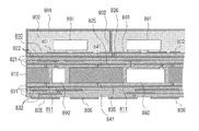
本実施の形態に係る通信モジュール100は、回路基板800の一方の主面に各種部品を表面実装するとともに、幾つかの部品を回路基板800に埋設し、回路基板800の部品実装面を樹脂などの封止部材で封止したものである。回路基板800の他方の主面には端子電極及びグランド電極が形成されている。通信モジュール100は、回路基板800の他方の主面を実装先の親回路基板に対向させ、前記端子電極及びグランド電極を親回路基板に半田付け等の手段で接続して使用される。以下、図2及び図3を参照して通信モジュール100の構造について説明する。図2は通信モジュールの各機能ブロックの配置を説明する平面図、図3は封止部材を取り除いた状態において通信モジュールを部品搭載面側からみた平面図である。
In the
通信モジュール100は、図2及び図3に示すように、横長矩形の回路基板800の左下側に形成され携帯電話用の高周波回路が実装される第1高周波処理部610と、回路基板800の右上部に形成され非携帯電話用の高周波回路が実装される第2高周波処理部620と、回路基板800の中央部から上部及び右部に向かって形成されベースバンド処理機能及びアプリケーション処理機能が実装されるシステム部630と、回路基板800の左上部に形成され各部に電源を供給する電源回路部640とに、機能的に区画されている。
2 and 3, the
第1高周波処理部610は、システム部630及び電源回路部640に隣接している。また、第1高周波処理部610には、図3に示すように、前述した高周波スイッチ101、デュプレクサ110,120、パワーアンプIC139、第1バンドパスフィルタ140、RFIC190が実装されている。また、第1高周波処理部610には、非携帯電話用の高周波回路部品の1つである第3バンドパスフィルタ340が実装されている。ここで、高周波スイッチ101、第1デュプレクサ110、パワーアンプIC139、RFIC190は回路基板800上に表面実装されている。一方、第2デュプレクサ120及び第3バンドパスフィルタ340は回路基板800内に埋設されている。また第1高周波処理部610における回路基板800の底面には、アンテナ11と接続するための端子(図示省略)が形成されている。なお、前述したように、ダイバーシティ受信回路や2系統同時通信用の送受信回路を構成するためのフロントエンド部品やRFICを設ける場合には、当該送受信回路を第1高周波処理部610に設けてもよい。
The first high
第2高周波処理部620は、図2に示すように、システム部630にのみ隣接している。換言すれば、第2高周波処理部620は、第1高周波処理部610及び電源回路部640には隣接していない。第2高周波処理部620には、図3に示すように、前述したダイプレクサ310、第4バンドパスフィルタ320、低雑音増幅器330、第6バンドパスフィルタ350、RFIC390が表面実装されている。また第2高周波処理部620における回路基板800の底面には、アンテナ20と接続するための端子(図示省略)が形成されている。
As shown in FIG. 2, the second high
システム部630は、図2に示すように、第1高周波処理部610、第2高周波処理部620、電源回路部640と隣接している。ここでシステム部630は、第1高周波処理部610と第2高周波処理部620との間に介在している点に留意されたい。またシステム部630には、図3に示すように、前述したベースバンドIC400とメモリ410が表面実装されている。ここでベースバンドIC400は、ベースバンド機能とアプリケーション機能が集積されている点に留意されたい。
As shown in FIG. 2, the
電源回路部640は、図2に示すように、システム部630及び第2高周波処理部620への電源供給を行う第1電源回路部641と、第1高周波処理部610への電源供給を行う第2電源回路部642とに、機能的に区画されている。第1電源回路部641は、システム部630及び第2電源回路部642に隣接しており、第1高周波処理部610及び第2高周波処理部620とは隣接していない。一方、第2電源回路部642は、システム部630、第1電源回路部641及び第1高周波処理部610と隣接しており、第2高周波処理部620とは隣接していない。第1電源回路部641には、図3に示すように、従来周知の主電源用の電源管理IC510、システムクロック発振子511、スイッチング処理用のインダクタ(図示省略)などの各種電子部品が実装されている。また、第2電源回路部642には、従来周知のDC/DCコンバータIC520及びDC/DCコンバータIC520のスイッチング処理用のインダクタ(図示省略)などの各種電子部品が実装されている。
As shown in FIG. 2, the power
本実施の形態に係る通信モジュール100は、図2で示したように、機能的に各部が区画されているが、さらに電気的及び物理的にも区画されている。本実施の形態では、第1高周波処理部610が形成された第1領域710、第2高周波処理部620が形成された第2領域720、電源回路部640の第1電源回路部641及びシステム部630が形成された第3領域730、電源回路部640の第2電源回路部642が形成された第4領域740に区画されている。各領域710〜740は、後述するように、回路基板800上に表面実装された各種部品を樹脂などの封止部材で封止したのちに、各領域が区画形成されるように回路基板800の表面まで封止部材に溝を形成し、封止部材表面全体を導電性材料で被覆してシールド層を形成するとともに前記溝にも導電性材料を充填してシールド壁902を形成することにより区画されている。なおシールド壁902の形成位置に対応する回路基板800の表面には基準電位(グランド電位)に設定されたグランド電極を形成しておき、前記シールド壁902と導通接続させる。
As shown in FIG. 2, the
次に図4を参照して回路基板の構造について説明する。図4は通信モジュールの断面図である。回路基板800は、絶縁体層と導体層とを積層してなる多層基板である。回路基板800は、図4に示すように、導電性が良好で且つ比較的厚い金属製の導体層であるコア層810と、該コア層810の一方の主面(上面)に形成された複数の絶縁体層821及び導体層822と、コア層810の他方の主面(下面)に形成された複数の絶縁体層831及び導体層832とを備えている。絶縁体層821,831及び導体層822,832はコア層810の両主面にビルドアップ工法にて形成されたものである。ここでコア層810と回路基板800の一方の主面(上面)との間に位置する導体層822のうち2つの層、及び、コア層810と回路基板800の他方の主面(下面)との間に位置する導体層832のうち1つの層は、基準電位(グランド)が与えられるグランド導体層825,826,835になっている。グランド導体層825,835は、コア層810に最も近い導体層822,832であり、それぞれビア導体841を介してコア層810に接続している。したがってコア層810もグランド導体として機能する。また、2つのグランド導体層825,826の間には導体層822が介在しており、該導体層822に形成された配線をストリップラインとして機能させることができる。回路基板800の一方の主面(上面)には部品実装用の導電性のランド801や配線802が形成されている。また、回路基板800の他方の主面(下面)には、マザーボードに接続するための端子電極805及びグランド電極806が形成されている。ランド801には、RFIC190やベースバンドIC400などの表面実装部品691が半田付けされている。
Next, the structure of the circuit board will be described with reference to FIG. FIG. 4 is a cross-sectional view of the communication module. The
コア層810には部品収容用の貫通孔811が形成されている。該貫通孔811には、SAWフィルタ、キャパシタ、インダクタなどの受動部品又はパワーアンプICなどの能動部品などの内蔵電子部品892が配置される。本実施の形態では、第2デュプレクサ120、第3バンドパスフィルタ340が貫通孔811内に配置される。したがって、コア層810は、内蔵電子部品892の高さよりも厚みが大きいことが好ましい。本実施の形態では、金属板、より詳しくは銅製又は銅合金製の金属板によりコア層810を形成している。貫通孔811内であって収容部品との隙間には樹脂などの絶縁体が充填されている。
The
回路基板800の上面すなわち部品実装面には、表面実装部品891を封止する封止部材900が形成されている。該封止部材900の材料としては、シリカやアルミナが添加されたエポキシ樹脂等の絶縁性樹脂が挙げられる。封止部材900の表面には導電性のシールド層901が形成されている。また封止部材900には、前述した各領域710〜740を区画するためのシールド壁902がシールド層901と一体となって形成されている。該シールド壁902の下端は回路基板800上面のグランド電極と接続している。
A sealing
以上詳述したように、本実施の形態に係る通信モジュール100によれば、携帯電話の構成に必要な主要機能部の多くが1つの通信モジュールに集約されているので高機能且つ小型化が図られる。ここで本実施の形態では、部品実装面である回路基板800の一方の主面に形成された封止部材900に、第1高周波処理部610とシステム部630及び電源回路部640とを区画するようにシールド壁902が形成されている。これによりシステム部630及び電源回路部640から第1高周波処理部610へのノイズの侵入を防止できるので高周波特性に優れたものとなる。また同様に、本実施の形態では、第2高周波処理部620とシステム部630とを区画するようにシールド壁902が形成されているので、更に高周波特性に優れたものとなる。さらに同様に、本実施の形態では、第1電源回路部641と第2電源回路部642とを区画するようにシールド壁902が形成されているので、更に高周波特性に優れたものとなる。
As described above in detail, according to the
また本実施の形態では、回路基板800がグランドとして機能するコア層810を備えており、該コア層810に形成された貫通孔811に電子部品が配置されているので、高密度化が図られるとともに埋設された電子部品は高いシールド性を有するものとなる。また本実施の形態では、回路基板810がコア層810を備えているので各機能部で発生した熱がコア層810に伝導し、さらに該コア層810において面方向に拡散する。これにより高い放熱効率が得られる。また本実施の形態では、回路基板800の一方の主面に全面に亘って電子部品を被覆する封止材料900が形成されているので、該封止部材900によっても高い放熱効率が得られる。
In the present embodiment, the
さらに本実施の形態では、回路基板800がコア層810を備えているので回路基板800は反りが生じにくく、さらに適切な封止部材900を選択することにより回路基板の反りを抑えることができる。
Further, in the present embodiment, since the
以上のように本実施の形態に係る通信モジュール800は、携帯電話の構成に必要な主要機能部の多くが集約されているにもかかわらず、高周波回路の特性劣化を防止でき、放熱効率が高く、反りが生じにくいものとなる。
As described above, the
以上本発明の一実施の形態について説明したが、本発明はこれに限定されるものではない。例えば上記実施の形態では、コア層810の材質として銅又は銅合金を例示したが、他の金属又は合金や樹脂など材質は不問である。また上記実施の形態では、回路基板800の上面には表面実装部品891を封止部材900により封止していたが、回路基板800の上面の全面又は一部を覆うように導電性のケースを装着するようにしてもよい。この場合、前記シールド壁902と対応するようにケース内にも導電性の仕切り壁を設けることが好ましい。
Although one embodiment of the present invention has been described above, the present invention is not limited to this. For example, in the above-described embodiment, copper or a copper alloy is exemplified as the material of the
また上記実施の形態では、電気的及び物理的に領域を区画するために、封止部材900の表面のシールド層901から回路基板800上のグランド電極まで延びるシールド壁902を設けていたが、図5に示すように、封止部材900の表面のシールド層901から封止部材900の厚み方向の略中間部まで延びたシールド壁903としてもよい。該シールド壁903は電気的及び物理的なシールド特性はシールド壁902よりもやや劣るものの、該シールド壁903の下方に表面実装部品691を配置することができる。したがって、上記実施の形態に係る通信モジュール100に対してシールド壁902や部品配置等を変更することなく、さらにシールド壁903を適宜追加することにより実装密度を維持しつつ電気的特性を向上させることができる。例えば上記実施の形態では電源回路部640の第1電源回路部641とシステム部630はシールド壁902により区画された同一の領域730内に実装されているが、電源回路部640の第1電源回路部641とシステム部630とを区画するようにシールド壁903を形成することが考えられる。
In the above embodiment, the
また上記実施の形態の回路は一例に過ぎず、他の回路構成であっても本発明を実施することができる。また、どの部品を埋設するかは、実装密度・シールド性・放熱性などを考慮して適宜選択すればよい。 The circuits in the above embodiments are merely examples, and the present invention can be implemented with other circuit configurations. In addition, which parts are to be embedded may be appropriately selected in consideration of mounting density, shielding properties, heat dissipation properties, and the like.
また上記実施の形態における各機能部の配置は一例に過ぎず、他の配置構成であっても本発明を実施できる。例えば、上記実施の形態では、第1高周波処理部610と第2高周波処理部620の間にシステム部630を配置していたが、第1高周波処理部610と第2高周波処理部620は隣接するようにしてもよい。この場合、必要に応じて、各処理部610及び620を電気的・物理的に区画するようにシールド壁902を形成してもよい。
In addition, the arrangement of the functional units in the above embodiment is merely an example, and the present invention can be implemented even with other arrangement configurations. For example, in the above embodiment, the
また上記実施の形態では、第1及び第2デュプレクサ110,120はそれぞれ送信フィルタ112,122及び受信フィルタ114,124を1つのパッケージに収容したものを用いたが、それぞれ個別のフィルタを用いてもよい。
In the above embodiment, the first and
また上記実施の形態では、コア層810に貫通孔811を形成し、該貫通孔811に第2デュプレクサ120などの電子部品を配置するようにしたが、貫通孔811ではなく凹部をコア層810に形成し、該凹部に各電子部品を配置するようにしてもよい。
In the above embodiment, a through
また上記実施の形態では、各通信に係るデジタル信号の処理機能であるベースバンド機能と、その他各種携帯電話のアプリケーション機能とを1つのベースバンドIC400に集積していたが、各機能を個別のICで実装するようにしてもよい。
In the above embodiment, the baseband function, which is a digital signal processing function related to each communication, and the application functions of various other mobile phones are integrated in one
また、上記実施の形態で説明した周波数帯域は一例に過ぎず、他の周波数帯域であっても本発明を実施できる。また、上記実施の形態で説明したGPSは衛星測位システムの一例に過ぎず、例えばロシアのGLONASSや中国のCompassなど他の衛星測位システムであっても本発明を実施できる。また、上記実施の形態では、分波器(アンテナ共用器)の例としてデュプレクサを挙げたが、トリプレクサなど3つ以上の通過周波数帯域を有する分波器であっても本発明を実施できる。 Moreover, the frequency band demonstrated by the said embodiment is only an example, and can implement this invention also in another frequency band. The GPS described in the above embodiment is merely an example of a satellite positioning system, and the present invention can be implemented even with other satellite positioning systems such as GLONASS in Russia and Compass in China. In the above embodiment, a duplexer is used as an example of a duplexer (antenna duplexer). However, the present invention can be implemented even with a duplexer having three or more pass frequency bands such as a triplexer.
11,20…アンテナ、110,120…デュプレクサ、112,122…送信フィルタ、114,124…受信フィルタ、131,132…高周波電力増幅器、139…パワーアンプIC、140,320,340,350…バンドパスフィルタ、190,390…RFIC、330…低雑音増幅器、310…ダイプレクサ、400…ベースバンドIC、610…第1高周波処理部、620…第2高周波処理部、630…システム部、640…電源回路部、800…回路基板、810…コア層、811…貫通孔
DESCRIPTION OF
Claims (5)
回路基板の一方の主面の全面に亘って形成され該主面に実装された電子部品を被覆する封止部材と、
封止部材の表面に形成された導電性のシールド層と、
前記システム部及び電源回路部の何れか一方又は双方の実装領域と前記第1高周波処理部の実装領域とを区画するように封止部材の主面から回路基板の一方の主面側に向かって形成された溝部を充填し且つ前記シールド層と導通した第1シールド壁とを備え、
前記電源回路部は第1高周波処理部用の第1電源回路部とシステム部用の第2電源回路部とを含み、
第1電源回路部の実装領域と第2電源回路部の実装領域とを区画するように封止部材の主面から回路基板の一方の主面側に向かって形成された溝部を充填し且つ前記シールド層と導通した第2シールド壁とを備えた
ことを特徴とする通信モジュール。 (A) a first high-frequency processing unit that processes a high-frequency signal related to mobile phone communication, (b) a baseband processing unit that processes a baseband signal related to mobile phone communication, and an application processing unit that processes various application operations of the mobile phone (C) a circuit board on which a power supply circuit unit is mounted;
A sealing member that covers the electronic component that is formed over the entire surface of one main surface of the circuit board and is mounted on the main surface;
A conductive shield layer formed on the surface of the sealing member;
From the main surface of the sealing member toward one main surface side of the circuit board so as to partition one or both of the mounting region of the system unit and the power supply circuit unit and the mounting region of the first high-frequency processing unit. A first shield wall filling the formed groove and electrically connected to the shield layer;
The power supply circuit unit includes a first power supply circuit unit for a first high-frequency processing unit and a second power supply circuit unit for a system unit,
Filling a groove formed from the main surface of the sealing member toward one main surface side of the circuit board so as to partition the mounting region of the first power circuit unit and the mounting region of the second power circuit unit; A communication module comprising a second shield wall that is electrically connected to the shield layer .
ことを特徴とする請求項1記載の通信モジュール。 The communication module according to claim 1, wherein a main processing unit of the baseband processing unit and a main processing unit of the application processing unit are integrated in one IC (Integrated Circuit).
回路基板の一方の主面の全面に亘って形成され該主面に実装された電子部品を被覆する封止部材と、
封止部材の表面に形成された導電性のシールド層と、
前記システム部及び電源回路部の何れか一方又は双方の実装領域と前記第1高周波処理部の実装領域とを区画するように封止部材の主面から回路基板の一方の主面側に向かって形成された溝部を充填し且つ前記シールド層と導通した第1シールド壁と、
前記回路基板に実装され非携帯電話通信に係る高周波信号を処理する第2高周波処理部と、
前記システム部及び電源回路部の何れか一方又は双方の実装領域と前記第2高周波処理部の実装領域とを区画するように封止部材の主面から回路基板の一方の主面側に向かって形成された溝部を充填し且つ前記シールド層と導通した第3シールド壁とを備えた
ことを特徴とする通信モジュール。 (A) a first high-frequency processing unit that processes a high-frequency signal related to mobile phone communication, (b) a baseband processing unit that processes a baseband signal related to mobile phone communication, and an application processing unit that processes various application operations of the mobile phone (C) a circuit board on which a power supply circuit unit is mounted;
A sealing member that covers the electronic component that is formed over the entire surface of one main surface of the circuit board and is mounted on the main surface;
A conductive shield layer formed on the surface of the sealing member;
From the main surface of the sealing member toward one main surface side of the circuit board so as to partition one or both of the mounting region of the system unit and the power supply circuit unit and the mounting region of the first high-frequency processing unit. A first shield wall filling the formed groove and in electrical communication with the shield layer;
A second high-frequency processing unit mounted on the circuit board for processing a high-frequency signal related to non-mobile phone communication;
From the main surface of the sealing member toward one main surface side of the circuit board so as to partition one or both of the mounting region of the system unit and the power supply circuit unit and the mounting region of the second high-frequency processing unit. A communication module, comprising: a third shield wall that fills the formed groove and is electrically connected to the shield layer.
ことを特徴とする請求項3記載の通信モジュール。 The communication module according to claim 3, wherein a mounting area of the system unit is disposed between a mounting area of the first high-frequency processing unit and a mounting area of the second high-frequency processing unit.
前記第1高周波処理部・システム部・電源回路部のうちの少なくとも何れか1つを構成する1つ以上の電子部品は前記回路基板のコア層に形成された貫通孔又は凹部内に配置されているOne or more electronic components constituting at least one of the first high-frequency processing unit, the system unit, and the power supply circuit unit are disposed in a through hole or a recess formed in the core layer of the circuit board. Have
ことを特徴とする請求項1乃至4何れか1項記載の通信モジュール。The communication module according to any one of claims 1 to 4, wherein the communication module is characterized in that:
Priority Applications (2)
| Application Number | Priority Date | Filing Date | Title |
|---|---|---|---|
| JP2013236650A JP5505915B1 (en) | 2013-10-30 | 2013-11-15 | Communication module |
| CN201410452261.7A CN104243642B (en) | 2013-10-30 | 2014-09-05 | Communication module |
Applications Claiming Priority (3)
| Application Number | Priority Date | Filing Date | Title |
|---|---|---|---|
| JP2013225216 | 2013-10-30 | ||
| JP2013225216 | 2013-10-30 | ||
| JP2013236650A JP5505915B1 (en) | 2013-10-30 | 2013-11-15 | Communication module |
Related Child Applications (1)
| Application Number | Title | Priority Date | Filing Date |
|---|---|---|---|
| JP2014047213A Division JP2015111802A (en) | 2013-10-30 | 2014-03-11 | Communication module |
Publications (2)
| Publication Number | Publication Date |
|---|---|
| JP5505915B1 true JP5505915B1 (en) | 2014-05-28 |
| JP2015111747A JP2015111747A (en) | 2015-06-18 |
Family
ID=50941876
Family Applications (3)
| Application Number | Title | Priority Date | Filing Date |
|---|---|---|---|
| JP2013236650A Expired - Fee Related JP5505915B1 (en) | 2013-10-30 | 2013-11-15 | Communication module |
| JP2014047213A Pending JP2015111802A (en) | 2013-10-30 | 2014-03-11 | Communication module |
| JP2014054606A Expired - Fee Related JP6285228B2 (en) | 2013-10-30 | 2014-03-18 | Communication module |
Family Applications After (2)
| Application Number | Title | Priority Date | Filing Date |
|---|---|---|---|
| JP2014047213A Pending JP2015111802A (en) | 2013-10-30 | 2014-03-11 | Communication module |
| JP2014054606A Expired - Fee Related JP6285228B2 (en) | 2013-10-30 | 2014-03-18 | Communication module |
Country Status (3)
| Country | Link |
|---|---|
| US (1) | US8849362B1 (en) |
| JP (3) | JP5505915B1 (en) |
| CN (1) | CN104243642B (en) |
Cited By (5)
| Publication number | Priority date | Publication date | Assignee | Title |
|---|---|---|---|---|
| JP2015146333A (en) * | 2014-01-31 | 2015-08-13 | 太陽誘電株式会社 | module |
| JP2022510411A (en) * | 2018-12-04 | 2022-01-26 | クリー インコーポレイテッド | How to form a packaged transistor device with separate inputs and outputs, and a packaged transistor device with separate inputs and outputs. |
| US11742304B2 (en) | 2018-07-19 | 2023-08-29 | Wolfspeed, Inc. | Radio frequency transistor amplifiers and other multi-cell transistors having isolation structures |
| US11757013B2 (en) | 2018-07-11 | 2023-09-12 | Wolfspeed, Inc. | Drain and/or gate interconnect and finger structure |
| US12057484B2 (en) | 2019-04-24 | 2024-08-06 | Macom Technology Solutions Holdings, Inc. | High power transistor with interior-fed fingers |
Families Citing this family (27)
| Publication number | Priority date | Publication date | Assignee | Title |
|---|---|---|---|---|
| JP5456935B1 (en) * | 2013-10-30 | 2014-04-02 | 太陽誘電株式会社 | Circuit module |
| KR102345584B1 (en) * | 2015-06-10 | 2021-12-31 | 삼성전자주식회사 | An electronic device and a method for controlling one or more antennas thereof |
| WO2017047539A1 (en) * | 2015-09-14 | 2017-03-23 | 株式会社村田製作所 | High-frequency module |
| JP6414559B2 (en) | 2016-02-22 | 2018-10-31 | 株式会社村田製作所 | Diplexer module with switch and diplexer module |
| JP2017200183A (en) * | 2016-04-29 | 2017-11-02 | スカイワークス ソリューションズ, インコーポレイテッドSkyworks Solutions, Inc. | Shielded diversity receiving module |
| WO2018181709A1 (en) | 2017-03-31 | 2018-10-04 | 株式会社村田製作所 | High frequency module |
| JP6965928B2 (en) | 2017-06-29 | 2021-11-10 | 株式会社村田製作所 | High frequency module |
| WO2019065027A1 (en) | 2017-09-29 | 2019-04-04 | 株式会社村田製作所 | Hybrid filter device and multiplexer |
| WO2019176778A1 (en) * | 2018-03-14 | 2019-09-19 | 株式会社村田製作所 | High frequency module and communication device |
| WO2019216299A1 (en) * | 2018-05-08 | 2019-11-14 | 株式会社村田製作所 | Method for manufacturing high-frequency module, and high-frequency module |
| JP7013323B2 (en) | 2018-05-17 | 2022-01-31 | 株式会社東芝 | Circuit equipment |
| CN109728405B (en) * | 2018-12-28 | 2022-03-01 | 维沃移动通信有限公司 | Antenna structure and high-frequency wireless communication terminal |
| CN109728447B (en) * | 2018-12-28 | 2023-01-13 | 维沃移动通信有限公司 | Antenna structure and high-frequency multi-band wireless communication terminal |
| KR102744902B1 (en) * | 2019-01-31 | 2024-12-20 | 삼성전자주식회사 | An electronic device comprising a housing comprising a metallic materials |
| WO2021002238A1 (en) * | 2019-07-03 | 2021-01-07 | 株式会社村田製作所 | High-frequency module and communication device |
| US11089673B2 (en) * | 2019-07-19 | 2021-08-10 | Raytheon Company | Wall for isolation enhancement |
| CN114788181B (en) * | 2019-12-20 | 2024-06-11 | 株式会社村田制作所 | High-frequency module and communication device |
| JP2021129194A (en) | 2020-02-13 | 2021-09-02 | 株式会社村田製作所 | High-frequency module and communication device |
| CN116057842A (en) | 2020-08-13 | 2023-05-02 | 株式会社村田制作所 | High frequency module and communication device |
| WO2022059457A1 (en) * | 2020-09-17 | 2022-03-24 | 株式会社村田製作所 | High-frequency module and communication device |
| WO2022065011A1 (en) * | 2020-09-24 | 2022-03-31 | 株式会社村田製作所 | High frequency module and communication device |
| WO2022065010A1 (en) | 2020-09-24 | 2022-03-31 | 株式会社村田製作所 | High-frequency module and communication device |
| CN116018676A (en) * | 2020-09-25 | 2023-04-25 | 株式会社村田制作所 | High-frequency module and communication device |
| WO2022138386A1 (en) * | 2020-12-25 | 2022-06-30 | 株式会社村田製作所 | High frequency module and communication apparatus |
| WO2022186131A1 (en) * | 2021-03-02 | 2022-09-09 | 株式会社村田製作所 | High frequency module and communication device |
| WO2023074251A1 (en) * | 2021-10-28 | 2023-05-04 | 株式会社村田製作所 | Tracker module |
| KR102409410B1 (en) * | 2021-12-29 | 2022-06-15 | 한화시스템 주식회사 | Transceivers for satellites and satellites |
Citations (3)
| Publication number | Priority date | Publication date | Assignee | Title |
|---|---|---|---|---|
| JPH0742187U (en) * | 1993-12-27 | 1995-07-21 | ミツミ電機株式会社 | Transceiver for wireless communication device |
| JP2012004725A (en) * | 2010-06-15 | 2012-01-05 | Renesas Electronics Corp | Semiconductor integrated circuit device and wireless communication system |
| JP5285806B1 (en) * | 2012-08-21 | 2013-09-11 | 太陽誘電株式会社 | High frequency circuit module |
Family Cites Families (11)
| Publication number | Priority date | Publication date | Assignee | Title |
|---|---|---|---|---|
| JP2005277939A (en) | 2004-03-25 | 2005-10-06 | Kyocera Corp | High frequency module and wireless communication device |
| WO2005099331A1 (en) * | 2004-03-30 | 2005-10-20 | Matsushita Electric Industrial Co., Ltd. | Module component and manufacturing method thereof |
| US8099064B2 (en) * | 2008-05-08 | 2012-01-17 | Research In Motion Limited | Mobile wireless communications device with reduced harmonics resulting from metal shield coupling |
| JP2011014659A (en) * | 2009-06-30 | 2011-01-20 | Murata Mfg Co Ltd | Composite electronic component module |
| US8592957B2 (en) * | 2009-08-18 | 2013-11-26 | Nec Corporation | Semiconductor device having shield layer and chip-side power supply terminal capacitively coupled therein |
| JP2011165931A (en) * | 2010-02-10 | 2011-08-25 | Mitsubishi Electric Corp | High-frequency circuit module |
| JP5380376B2 (en) * | 2010-06-21 | 2014-01-08 | 日立オートモティブシステムズ株式会社 | Power semiconductor device |
| JP2012019091A (en) * | 2010-07-08 | 2012-01-26 | Sony Corp | Module and portable terminal |
| KR101862370B1 (en) * | 2011-05-30 | 2018-05-29 | 삼성전자주식회사 | Semiconductor device, a semiconductor package and a electronic device |
| US8766654B2 (en) * | 2012-03-27 | 2014-07-01 | Universal Scientific Industrial Co., Ltd. | Package structure with conformal shielding and inspection method using the same |
| JP5117632B1 (en) * | 2012-08-21 | 2013-01-16 | 太陽誘電株式会社 | High frequency circuit module |
-
2013
- 2013-11-15 JP JP2013236650A patent/JP5505915B1/en not_active Expired - Fee Related
-
2014
- 2014-03-06 US US14/199,824 patent/US8849362B1/en not_active Expired - Fee Related
- 2014-03-11 JP JP2014047213A patent/JP2015111802A/en active Pending
- 2014-03-18 JP JP2014054606A patent/JP6285228B2/en not_active Expired - Fee Related
- 2014-09-05 CN CN201410452261.7A patent/CN104243642B/en not_active Expired - Fee Related
Patent Citations (3)
| Publication number | Priority date | Publication date | Assignee | Title |
|---|---|---|---|---|
| JPH0742187U (en) * | 1993-12-27 | 1995-07-21 | ミツミ電機株式会社 | Transceiver for wireless communication device |
| JP2012004725A (en) * | 2010-06-15 | 2012-01-05 | Renesas Electronics Corp | Semiconductor integrated circuit device and wireless communication system |
| JP5285806B1 (en) * | 2012-08-21 | 2013-09-11 | 太陽誘電株式会社 | High frequency circuit module |
Cited By (6)
| Publication number | Priority date | Publication date | Assignee | Title |
|---|---|---|---|---|
| JP2015146333A (en) * | 2014-01-31 | 2015-08-13 | 太陽誘電株式会社 | module |
| US11757013B2 (en) | 2018-07-11 | 2023-09-12 | Wolfspeed, Inc. | Drain and/or gate interconnect and finger structure |
| US11742304B2 (en) | 2018-07-19 | 2023-08-29 | Wolfspeed, Inc. | Radio frequency transistor amplifiers and other multi-cell transistors having isolation structures |
| JP2022510411A (en) * | 2018-12-04 | 2022-01-26 | クリー インコーポレイテッド | How to form a packaged transistor device with separate inputs and outputs, and a packaged transistor device with separate inputs and outputs. |
| JP7382405B2 (en) | 2018-12-04 | 2023-11-16 | ウルフスピード インコーポレイテッド | Packaged transistor device with separated input and output and method of forming a packaged transistor device with separated input and output |
| US12057484B2 (en) | 2019-04-24 | 2024-08-06 | Macom Technology Solutions Holdings, Inc. | High power transistor with interior-fed fingers |
Also Published As
| Publication number | Publication date |
|---|---|
| CN104243642A (en) | 2014-12-24 |
| JP6285228B2 (en) | 2018-02-28 |
| JP2015111747A (en) | 2015-06-18 |
| US8849362B1 (en) | 2014-09-30 |
| JP2015111803A (en) | 2015-06-18 |
| CN104243642B (en) | 2016-03-30 |
| JP2015111802A (en) | 2015-06-18 |
Similar Documents
| Publication | Publication Date | Title |
|---|---|---|
| JP5505915B1 (en) | Communication module | |
| US9160825B2 (en) | Communication module | |
| JP5677499B2 (en) | High frequency circuit module | |
| JP5456935B1 (en) | Circuit module | |
| JP5143972B1 (en) | High frequency circuit module | |
| KR101445543B1 (en) | High-frequency circuit module | |
| JP5117632B1 (en) | High frequency circuit module | |
| JP5342704B1 (en) | High frequency circuit module | |
| JP2006340257A (en) | Multi-mode high frequency circuit | |
| JP4709316B2 (en) | Multimode high frequency circuit | |
| JP5422078B1 (en) | High frequency circuit module | |
| CN104602366B (en) | Communication module | |
| JP5420104B1 (en) | High frequency circuit module | |
| JP2014039236A (en) | High-frequency circuit module | |
| JP5420102B1 (en) | High frequency circuit module | |
| JP5420101B1 (en) | High frequency circuit module | |
| JP2005136887A (en) | High frequency module and wireless communication device | |
| JP5420103B1 (en) | High frequency circuit module | |
| JP2006211144A (en) | High frequency module and wireless communication device | |
| JP2006203470A (en) | High frequency module and wireless communication device |
Legal Events
| Date | Code | Title | Description |
|---|---|---|---|
| TRDD | Decision of grant or rejection written | ||
| A01 | Written decision to grant a patent or to grant a registration (utility model) |
Free format text: JAPANESE INTERMEDIATE CODE: A01 Effective date: 20140212 |
|
| RD02 | Notification of acceptance of power of attorney |
Free format text: JAPANESE INTERMEDIATE CODE: A7422 Effective date: 20140220 |
|
| RD04 | Notification of resignation of power of attorney |
Free format text: JAPANESE INTERMEDIATE CODE: A7424 Effective date: 20140221 |
|
| A61 | First payment of annual fees (during grant procedure) |
Free format text: JAPANESE INTERMEDIATE CODE: A61 Effective date: 20140311 |
|
| R150 | Certificate of patent or registration of utility model |
Ref document number: 5505915 Country of ref document: JP Free format text: JAPANESE INTERMEDIATE CODE: R150 |
|
| R250 | Receipt of annual fees |
Free format text: JAPANESE INTERMEDIATE CODE: R250 |
|
| R250 | Receipt of annual fees |
Free format text: JAPANESE INTERMEDIATE CODE: R250 |
|
| R250 | Receipt of annual fees |
Free format text: JAPANESE INTERMEDIATE CODE: R250 |
|
| R250 | Receipt of annual fees |
Free format text: JAPANESE INTERMEDIATE CODE: R250 |
|
| R250 | Receipt of annual fees |
Free format text: JAPANESE INTERMEDIATE CODE: R250 |
|
| LAPS | Cancellation because of no payment of annual fees |