JP5485496B2 - Semiconductor test equipment - Google Patents
Semiconductor test equipment Download PDFInfo
- Publication number
- JP5485496B2 JP5485496B2 JP2006340597A JP2006340597A JP5485496B2 JP 5485496 B2 JP5485496 B2 JP 5485496B2 JP 2006340597 A JP2006340597 A JP 2006340597A JP 2006340597 A JP2006340597 A JP 2006340597A JP 5485496 B2 JP5485496 B2 JP 5485496B2
- Authority
- JP
- Japan
- Prior art keywords
- light
- wavelength
- signal
- optical
- converted
- Prior art date
- Legal status (The legal status is an assumption and is not a legal conclusion. Google has not performed a legal analysis and makes no representation as to the accuracy of the status listed.)
- Active
Links
- 238000012360 testing method Methods 0.000 title claims description 50
- 239000004065 semiconductor Substances 0.000 title claims description 28
- 230000003287 optical effect Effects 0.000 claims description 101
- 238000006243 chemical reaction Methods 0.000 claims description 49
- 239000013307 optical fiber Substances 0.000 claims description 18
- 239000000835 fiber Substances 0.000 claims description 16
- 230000001934 delay Effects 0.000 claims description 5
- 230000000737 periodic effect Effects 0.000 claims description 3
- 230000010287 polarization Effects 0.000 claims description 3
- 230000000644 propagated effect Effects 0.000 claims 1
- 238000010586 diagram Methods 0.000 description 12
- 230000003111 delayed effect Effects 0.000 description 6
- 229910013641 LiNbO 3 Inorganic materials 0.000 description 5
- 230000007274 generation of a signal involved in cell-cell signaling Effects 0.000 description 4
- 239000000758 substrate Substances 0.000 description 4
- 230000001360 synchronised effect Effects 0.000 description 3
- GQYHUHYESMUTHG-UHFFFAOYSA-N lithium niobate Chemical compound [Li+].[O-][Nb](=O)=O GQYHUHYESMUTHG-UHFFFAOYSA-N 0.000 description 2
- 230000005540 biological transmission Effects 0.000 description 1
- 230000015556 catabolic process Effects 0.000 description 1
- 238000004891 communication Methods 0.000 description 1
- 239000013078 crystal Substances 0.000 description 1
- 238000006731 degradation reaction Methods 0.000 description 1
- 230000000694 effects Effects 0.000 description 1
- CPLXHLVBOLITMK-UHFFFAOYSA-N magnesium oxide Inorganic materials [Mg]=O CPLXHLVBOLITMK-UHFFFAOYSA-N 0.000 description 1
- 239000000395 magnesium oxide Substances 0.000 description 1
- AXZKOIWUVFPNLO-UHFFFAOYSA-N magnesium;oxygen(2-) Chemical compound [O-2].[Mg+2] AXZKOIWUVFPNLO-UHFFFAOYSA-N 0.000 description 1
- 239000000463 material Substances 0.000 description 1
- 238000000034 method Methods 0.000 description 1
- 238000012986 modification Methods 0.000 description 1
- 230000004048 modification Effects 0.000 description 1
- 238000012545 processing Methods 0.000 description 1
- 230000000630 rising effect Effects 0.000 description 1
- 230000008054 signal transmission Effects 0.000 description 1
- 230000002123 temporal effect Effects 0.000 description 1
Images


Landscapes
- Testing Of Optical Devices Or Fibers (AREA)
- Optical Communication System (AREA)
Description
本発明は、ジッタ付加装置および半導体試験装置に関する。より詳細には、信号光に所望のジッタを付加するジッタ付加装置、および、当該ジッタ付加装置を備える試験装置に関する。 The present invention relates to a jitter adding apparatus and a semiconductor test apparatus. More specifically, the present invention relates to a jitter adding apparatus that adds desired jitter to signal light, and a test apparatus including the jitter adding apparatus.
信号光を出射または受光する半導体光デバイスを試験する種々の方法および装置がある。特に、光デバイスにおけるジッタに対する耐性を試験すべく、信号光にジッタを付加して試験する試験装置がある(例えば、特許文献1)。下記特許文献1には、電気的な試験信号にジッタを重畳し、ジッタが重畳された試験信号を光信号に変換して、光通信システムの試験信号として用いることが記載されている。
しかしながら、電気的な試験信号にジッタを重畳する場合に、電気信号では応答速度が限られるので微小量のジッタを試験信号に重畳することが困難である。また、電気回路では、光信号に対して直接にジッタを付加できない。このため、例えば、光入出力モジュールのループバック試験をおいて光信号を受信する側のジッタ耐性等を単独で評価しようとしても、送信側の発生した光信号に非同期のジッタを付加することができない。 However, when jitter is superimposed on an electrical test signal, the response speed of the electrical signal is limited, so it is difficult to superimpose a small amount of jitter on the test signal. In addition, the electric circuit cannot add jitter directly to the optical signal. For this reason, for example, even when trying to independently evaluate the jitter tolerance of the optical signal receiving side in the loopback test of the optical input / output module, asynchronous jitter may be added to the optical signal generated on the transmitting side. Can not.
そこで、上記課題を解決すべく、本発明の第1の形態として、特定波長のパルス光である信号光にジッタを付加して出力する光ジッタ付加装置であって、互いに異なる波長を有する制御光を出力する制御光源と、信号光が入力された場合は特定波長の信号光を非変換光として出力し、互いに異なる波長の制御光のうちいずれかおよび信号光が時間的に重畳して入力された場合は、制御光の波長に対応した、特定波長とは異なる変換波長に信号光の波長を変換した変換光を出力する波長変換素子と、波長変換素子から出力された非変換光および変換光を入力されて、波長に応じて異なる遅延量で遅延させて出力することにより、前記信号光にジッタを付加して出力する遅延部とを備える光ジッタ付加装置が提供される。 Accordingly, in order to solve the above-described problem, as a first embodiment of the present invention, an optical jitter adding apparatus for adding jitter to signal light that is pulsed light having a specific wavelength and outputting the signal light, the control light having different wavelengths. When a signal light is input, a signal light of a specific wavelength is output as non-converted light, and one of the control lights having different wavelengths and the signal light are temporally superimposed and input. The wavelength conversion element that outputs the converted light obtained by converting the wavelength of the signal light to the conversion wavelength different from the specific wavelength, corresponding to the wavelength of the control light, and the non-converted light and the converted light output from the wavelength conversion element. Is provided with a delay unit that adds a jitter to the signal light and outputs the delayed signal light.
更に、本発明の第2の形態として、特定波長のパルス光である信号光にジッタを付加して半導体光デバイスを試験する半導体試験装置であって、半導体光デバイスに信号光を発生させる電気的な試験信号を発生する信号発生器と、互いに異なる波長を有する制御光を出力する制御光源と、信号光が入力された場合は特定波長の信号光を非変換光として出力し、信号光および互いに異なる波長の制御光のうちのいずれかが時間的に重畳して入力された場合は、制御光の波長に対応した、特定波長とは異なる変換波長に信号光の波長を変換した変換光を出力する波長変換素子と、波長変換素子から出力された非変換光および変換光が入力されて、その波長に応じて異なる遅延量で遅延させることにより、信号光にジッタを付加して出力する遅延部とを備える。 Furthermore, as a second embodiment of the present invention, there is provided a semiconductor test apparatus for testing a semiconductor optical device by adding jitter to signal light which is pulsed light of a specific wavelength, and an electrical device for generating signal light in the semiconductor optical device. A signal generator that generates a test signal, a control light source that outputs control light having different wavelengths, and when signal light is input, the signal light having a specific wavelength is output as non-converted light. If any of the control lights of different wavelengths are input in a time-superimposed manner, the converted light converted from the signal light wavelength to a conversion wavelength different from the specific wavelength corresponding to the control light wavelength is output. And a delay unit that receives the non-converted light and the converted light output from the wavelength converting element and delays them with a different delay amount according to the wavelength, thereby adding jitter to the signal light and outputting it. Equipped with a.
なお、上記の発明の概要は、本発明の必要な特徴の全てを列挙したものではない。従って、これらの特徴群のサブコンビネーションもまた発明となり得る。 It should be noted that the above summary of the invention does not enumerate all the necessary features of the present invention. Therefore, a sub-combination of these feature groups can also be an invention.
以下、発明の実施の形態を通じて本発明を説明するが、以下の実施形態は特許請求の範囲に係る発明を限定するものではない。また、実施形態の中で説明されている特徴の組み合わせの全てが発明の解決手段に必須であるとは限らない。 Hereinafter, the present invention will be described through embodiments of the invention, but the following embodiments do not limit the invention according to the claims. In addition, not all the combinations of features described in the embodiments are essential for the solving means of the invention.
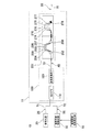
図1は、光信号にジッタを付加する光ジッタ付加装置10の構成を模式的に示す図である。同図に示すように、光ジッタ付加装置10は、信号光を発生する信号光源20とは別の波長可変制御光源30と、信号光源20および波長可変制御光源30の出力に、光ファイバ71、72を介して接続された波長変換部100と、波長変換部100の出力に光ファイバ73を介して接続された遅延部200とを備える。また、波長可変制御光源30の出力する制御光の波長を選択する波長制御信号を発生する波長制御信号発生部32を備える。
FIG. 1 is a diagram schematically showing the configuration of an optical
信号光源20は、試験のためにパルス幅およびパルス間隔が所定のパターンに変調された、特定波長λ1を有するパルス光を発生する。この場合に、信号光源20は、半導体試験装置のパターン発生器により発生した所定のパターンの電気的な試験信号に基づいて、上記パルス光を発生する。一方、波長可変制御光源30は、波長制御信号発生部32の発生した波長制御信号を受けて、相互に異なる複数の波長λ11、λ12、λ13から選択されたいずれかの波長を有する制御光35を発生する。信号光源20の一例は、パルスレーザであるが、これに限られず、CWレーザと変調器との組み合わせ等であってもよい。一方、波長可変制御光源30の一例は、例えばDFBレーザである。DFBレーザは、1パルス単位でON−OFF制御してパルス光を発生することができる。
The
波長変換部100は、信号光源20の出力する信号光25および波長可変制御光源30の出力する制御光35の両方を合波して波長変換素子120に結合する光カプラ110と、光カプラ110の出力を受ける波長変換素子120とを有する。ここで、波長変換部100に信号光25が単独で入力された場合、波長変換素子120は信号光25をそのままの波長で出力する。一方、信号光25および制御光35が両方入力された場合は、後述するように、信号光25の波長を制御光35の波長に応じて変換して変換光45を出力する。なお、説明の便宜のために、以下の記載では、信号光25の波長から変換されることなく波長変換素子120から出力された光も含めて、波長変換素子120から出力される光信号をすべて変換光45と記載する。
The
遅延部200は、波長変換部100から出力された変換光45を入力される。入力された変換光45は、光サーキュレータ220を介して光遅延線210に注入される。光遅延線210は、入力された変換光45に対してその波長に応じた異なる量の遅延を与えて、遅延光として再び光サーキュレータ220に戻す。光サーキュレータ220は、光遅延線210から入力された遅延光を光ファイバ75に結合して、出力光55として外部に出力する。
The
ここで、光遅延線210は、それ自体が光ファイバであり、更に、その長さ方向について異なる位置に形成された複数のファイバグレーティング部212、214、216、218を有する。ファイバグレーティング部212、214、216、218は、それぞれ一定の間隔で形成された複数のグレーティングを有して、ブラッグ格子を形成する。ブラッグ格子は、グレーティングを形成された光ファイバの屈折率、および、グレーティングにおいて変化した屈折率の差の積を2倍にして得られる波長(以下、「ブラッグ波長」と記載する)を中心とする狭帯域の光を反射する。従って、ファイバグレーティング部212、214、216、218の各々では、それぞれ固有の波長の光が反射される。光遅延線210の入射端からファイバグレーティング部212、214、216、218の各々までの距離は互いに異なるので、光遅延線210へ入射されてから出射に至るまでの光の経路長は変換光45の波長に応じて異なる。
Here, the
なお、図1に示す光ジッタ付加装置10の遅延部200において、光遅延線210の入射端に最も近いファイバグレーティング部212は、信号光25の波長λ1と等しいブラッグ波長λ1を有するものとする。また、他のファイバグレーティング部214、216、218のブラッグ波長λ21、λ22、λ23は順次長くなるものとする。
In the
上記ジッタ付加装置10において、信号光源20は、特定波長λ1のパルス光である信号光25を出力する。また、波長可変制御光源30は、互いに異なる波長λ11、λ12、λ13のうち、波長制御信号発生部32が発生した波長制御信号により選択されたいずれかの波長を有する制御光35を出力する。
In the
波長変換素子120は、信号光25が単独で入力された場合は特定波長λ1の信号光25を出力する。一方、波長変換素子120は、波長λ11、λ12、λ13のいずれかを有する制御光35と信号光25とが時間的に重畳して入力された場合に、制御光35の波長λ11、λ12、λ13に応じて、特定波長λ1とは異なる変換波長λ21、λ22、λ23に信号光25の波長λ1を変換した変換光45を出力する。遅延部200は、波長変換素子120から出力された信号光25および変換光45を入力されて、波長λ1、λ21、λ22、λ23に応じて異なる遅延量Δt1、Δt2、Δt3で遅延させて出力する。
The
このように、光ジッタ付加装置10は、光信号に対して直接に所望のジッタを付加できる。従って、例えば、光入出力モジュールのループバック試験をおいて、送信側の発生した光信号に所望のジッタを付加して、受信側のジッタ耐性等を単独で評価できる。
As described above, the optical
図2は、波長変換素子120として使用できるPPLN(Periodically Poled LiNbO3)導波路の構造を示す斜視図である。同図に示すように、PPLN導波路は、非常に短い周期で分極が反転する非線形光学結晶であるLiNbO3基板122と、反転する分極分布を横切るようにLiNbO3基板122に形成された光導波路124とを有する。このような構造を有する波長変換素子120に波長の異なる2つのレーザ光を注入した場合、それらレーザ光の和周波光または差周波光が出射される。
FIG. 2 is a perspective view showing a structure of a PPLN (Periodically Poled LiNbO 3 ) waveguide that can be used as the
波長変換素子120としては、例えば、周期分極反転ニオブ酸リチウム(PPLN)光導波路により形成できる。周期分極反転ニオブ酸リチウム光導波路は、特定波長λ1の信号光25と波長λ11、λ12、λ13のいずれかを有する制御光35とを入力された場合に、強い光強度で入力された一方の光の第二高調波と他方の光との差周波の波長を有する変換光45を出力する。従って、波長制御信号発生部32により制御光35の波長λ11、λ12、λ13を選択して高効率に信号光25を波長変換させることにより、波長変換素子120に所望の波長の変換光45を出力させることができる。
The
なお、LiNbO3は、室温では可視光により光損傷を受けることが知られている。従って、酸化マグネシウム等を添加して材料の安定性を増すことが好ましい。また、上記のような波長変換素子において変換の対象となるのは、TMモードの直線偏光である信号光25および制御光35であるか、あるいは、信号光25および制御光35に含まれるTMモードの直線偏光成分である。
LiNbO 3 is known to be damaged by visible light at room temperature. Therefore, it is preferable to add magnesium oxide or the like to increase the stability of the material. Further, in the wavelength conversion element as described above, the
図3は、上記のようなPPLN導波路を有する波長変換素子120の動作を説明する図である。同図に示すように、波長変換素子120には、互いに異なる波長λ11、λ12、λ13を有する複数の制御光35のいずれかと、特定波長λ1を有する信号光25とが注入される。ここで、信号光25の光強度が十分に高い場合、信号光25の第二高調波が発生し、更に、制御光35および第二高調波の差周波に相当する波長λ21、λ22、λ23を有する変換光45が出射される。従って、波長制御信号発生部32を介して制御光35の波長λ11、λ12、λ13を選択することにより、変換光45の波長を波長λ21、λ22、λ23のいずれかとすることができる。
FIG. 3 is a diagram for explaining the operation of the
なお、波長変換素子120の構造は、PPLN導波路に限定されるに限定されるわけではなく、例えば、周期分極反転構造を持ったLiB3O5、BaB2O4、KTiOPO4、LiTaO3等を用いることもできる。また、半導体光増幅器SOA(Semiconductor Optical Amplifier)などの非線形光学素子を用いても同様の作用を得ることができる。また、非線形光ファイバ、電界吸収型変調器などを用いることもできる。
The structure of the
図4は、パルス光として信号光源20から出力される信号光25、パルス光として波長可変制御光源30から出力される制御光35、および、波長変換部100から出力される変換光45の相互のタイミングを比較して示す図である。なお、変換光45は、制御光35が入力されず、信号光25の波長がそのまま維持されるものも含んでいる。
FIG. 4 shows the mutual relationship between the
同図に示すように、信号光25は、所定の立ち上がりと立ち下がりのパターンを有する波長λ1のパルス光である。なお図4では説明のために、一定間隔のタイミングで立ち上がり、一定のパルス幅を有する波長λ1のパルス光を示した。これに対して、制御光35は、信号光25の特定のパルスに同期したタイミングで立ち上がるワンショットのパルスを含むパルス光となる。また、制御光35は、一定のパルス幅を有するもパルスの各々が個別の波長λ11、λ12、λ13を有する。ここで、制御光35のパルス幅は信号光25のパルス幅と等しいからそれよりも広くすることが好ましい。ただし、制御光35のパルス幅は、波長変換の対象となる信号光25の特定のパルスに隣接する他のパルスに影響を与えない程度の幅に制限することが好ましい。
As shown in the figure, the
波長変換部100に入射した信号光25および制御光35は、パルス単位で同期しながら光カプラ110において合波された後、波長変換素子120に注入される。波長変換素子120から出射される変換光45は、信号光25のパルスと制御光35のパルスが時間的に重畳された期間については、制御光35の波長λ11、λ12、λ13に対応して波長変換された波長λ21、λ22、λ23を有するパルスを含む。一方、波長変換素子120に信号光25が単独で入射されたとき、即ち、図4において制御光35に対応する(時間的に重畳された)パルスがない期間については波長変換されることかなく、信号光25の波長λ1を維持したままの非変換光が波長変換部100から出射される。従って、変換光45は、信号光25の波長λ1を有するパルスと、波長変換された波長λ21、λ22、λ23を有するパルスとを含む。
The
図5は、変換光45および出力光55の相互のタイミングを比較して示す図である。前記したように、遅延部200の光遅延線210は、信号光25の波長λ1と同じブラッグ波長λ1を有するファイバグレーティング部212を有する。また、各々が固有のブラッグ波長ブラッグ波長λ21、λ22、λ23を有するファイバグレーティング部214、216、218を有する。従って、光遅延線210に入射された変換光45の各パルスは、それぞれが有する波長λ1、λ21、λ22、λ23に応じて個別のファイバグレーティング部212、214、216、218において反射される。
FIG. 5 is a diagram comparing the timings of the converted
また、ファイバグレーティング部212、214、216、218は相互に、光遅延線210の入射端からの距離を異にしている。従って、光遅延線210に入射してから出射するまでの光の経路長は、各パルスの波長λ1、λ21、λ22、λ23に応じて異なる。このため、図5に示すように、変換光45の波長に応じて、出力光55のパルスには個別の遅延量Δt1、Δt2、Δt3が与えられる。換言すれば、波長可変制御光源30の発生する制御光35の波長を選択することにより、出力光55に所望の大きさのジッタを付加することができる。
Further, the
このように、遅延部200は、入力された変換光45を、特定波長λ1および変換波長λ21、λ22、λ23に応じてそれぞれ選択的に反射する複数のファイバグレーティング部212、214、216、218を信号光25および制御光35の通過方向に形成された光ファイバを用いて形成できる。これにより、簡単な構造で、波長λ1、λ21、λ22、λ23に応じて異なる量Δt1、Δt2、Δt3の遅延を生じさせることができる。
In this way, the
なお、上記の実施形態では、信号光25のパルスのタイミングに対して遅れるジッタを発生する。しかしながら、信号光25の波長λ1と同じブラッグ波長λ1を有するファイバグレーティング部212の配置を変更して、光遅延線210の入射端により接近した位置に他のファイバグレーティング部214、216、218を配置することにより、信号光25のパルスのタイミングに対して進んだジッタを発生させることもできる。
In the above embodiment, jitter that is delayed with respect to the timing of the pulse of the
この光ジッタ付加装置10は、信号光25をパルスごとに遅延させて所望のジッタを付加することができる。また、ジッタの付加に係る信号処理においては、光信号を電気信号に変換することがないので、装置の構成を簡素にできる。更に、光−電気変換に伴う信号劣化も生じない。なお、図1において点線で囲って示す波長変換部100および遅延部200を組み合わせて、光ジッタ付加ユニット11を形成して単独で供給することもできる。
The optical
このように、特定波長λ1のパルス光である信号光25を入力されて、信号光25にジッタを付加して出力する光ジッタ付加ユニット11であって、信号光25が入力された場合は特定波長λ1の非変換光を出力して、互いに異なる波長λ21、λ22、λ23の制御光35のうちいずれかおよび信号光25が時間的に重畳して入力された場合は、制御光35の波長λ11、λ12、λ13に対応した、特定波長λ1とは異なる変換波長λ21、λ22、λ23に信号光25の波長λ1を変換した変換光45を出力する波長変換素子120と、波長変換素子120から出力された信号光25および変換光45を入力されて、波長λ1、λ21、λ22、λ23に応じて異なる遅延量Δt1、Δt2、Δt3で遅延させて出力する遅延部200とを備える光ジッタ付加ユニット11が提供される。この光ジッタ付加ユニット11は、既存の光信号伝送系に装着して、ジッタを付加する機能を追加することができる。
As described above, when the
なお、上記実施形態において、光遅延線210は、異なる波長で反射するファイバグレーティング部212、214、216、218を軸方向の異なる位置に配するが、光遅延線210の構成はこれに限られない。他の光遅延線210として、波長λ1、λ23を含む波長領域で反射するように、ピッチが軸方向について連続的に変化するチャープドFBGを用いてもよい。この場合に、制御光の波長によって変換光の波長を変えることで、連続して遅延量を変えることができる。
In the above embodiment, the
図6は、他の実施形態に係る光ジッタ付加装置10の構造を模式的に示す図である。同図に示すように、この光ジッタ付加装置10は、図1に示した光ジッタ付加装置10に対して、遅延部200の光遅延線210に換えてAWG(アレイド・ウェーブガイド・グレーティング)を用いて形成した遅延部201を備える点が異なる。図6に示すように、遅延部201は、AWG(アレイド・ウェーブガイド・グレーティング)分波器250、および、このAWG分波器250に連結された遅延線270を有する。また、波長可変制御光源30の出力する制御光の波長を選択する波長制御信号を発生する波長制御信号発生部32も備える。
FIG. 6 is a diagram schematically showing the structure of the optical
AWG分波器250は、一対のスラブ導波路252、258およびこれらの間に配された複数のアレイ導波路254、255、256、257を有する。このAWG分波器250は、波長変換部100から光ファイバ73を介して入力される変換信号光45に含まれる非変換光および変換光をそれぞれの波長に応じて分光して後段のスラブ導波路258において異なる導波路から出力する。
The AWG duplexer 250 has a pair of
また、遅延線270は、複数のアレイ導波路274、275、276、277、および、合波器278を有する。これら複数のアレイ導波路274、275、276、277は、互いに長さが異なる。この遅延線270は、AWG分波器250の異なる導波路から出力されたそれぞれの光を、対応する複数のアレイ導波路274、275、276,277に入力し、合波部278において一つの光ファイバ75に出力する。このとき、アレイ導波路274はアレイ導波路275よりも経路長が長いので、例えば変換信号光45のうち変換光がアレイ導波路274を通り、非変換光がアレイ導波路275を通る場合に、変換光は非変換光に対して時間的に遅延する。ここで、変換光がアレイ導波路275を通り、非変換光がアレイ導波路274を通る場合に、遅延部出力光55における変換光および非変換光の時間的な遅延関係は逆になる。
The
このように、光可変遅延装置11の遅延部201は、非変換光および変換光の一方を他方に対して時間的に遅延させて出力することができる。これにより、図5に示した光遅延線210の場合と同様に、波長制御信号発生部32の制御の下に選択された制御光35の波長λ11、λ12、λ13に応じた固有の波長λ21、λ22、λ23を有するパルスに対して、光導波路332、234、236、238の長さに応じた遅延を与えてジッタを付加することができる。
As described above, the
図7は、上記の遅延部202の他の実施形態に係る構造を示す図である。図7の光可変遅延装置10において、図6の光可変遅延装置10と同じ構成については同じ参照番号を付して説明を省略する。図7の遅延部202は、図6に示すAWG分波器250と、このAWG分波器250に接続された光ファイバ281、282、283、284、と、これらの光ファイバ281、282、283、284、に接続された合波器278とを有する。このような構成によれば、光ファイバ281、282、283、284の長さを調節することにより、分光部231により分光された非変換光および変換光の通過する経路長を所望に設定することができる。したがって、光可変遅延装置10は、遅延部出力光55に含まれる非変換光および変換光の一方を他方に対してより大きなジッタを付加することができる。
FIG. 7 is a diagram illustrating a structure according to another embodiment of the
図8は、また他の実施形態における波長可変制御光源300の構造を示す模式図である。同図に示すように、この波長可変制御光源300は、光源として複数の発光素子312、214、316と、これら発光素子312、314、316に電流を供給する電源362、364、366と、この電流を変調する変調器372、374、376を有する。ここで、発光素子312、314、316は、変調器372、374、376により変調された電流に対応して出射光32、34、36の波長を変えることができる。この場合に、発光素子312、314、316のそれぞれの出力する出射光32、34、36の波長が変化する範囲が互いに隣接するように設定されることが好ましい。これにより、単一の発光素子312、314、316が発光できる波長範囲に制限されることなく、所望の広い範囲で変化する制御光38を発生することができる。
FIG. 8 is a schematic diagram showing the structure of a wavelength tunable control
また、波長可変制御光源300は、発光素子312、214、316に出力に接続され、各出力を個別に断続する光スイッチ322、324、326と、光スイッチ322、324、326の出力を単一の制御光38として出力する光マルチプレクサ340とを備える。また、制御光38は、光スイッチ322、324、326および光マルチプレクサ340における光信号の減衰を補償する光ファイバ増幅器350を介して、図1または図6に示した波長変換部100の光カプラ110に結合される。
In addition, the wavelength tunable control
ここで、発光素子312、214、316は、互いに隣接して異なる一定の範囲で発光波長を変化させることができる。また、光スイッチ322、324、326は、ひとつの駆動源338に対して選択的に結合される制御端子332、334、336により選択的に投入され、発光素子312、314、316のいずれかの出射光32、34、36が、制御光38として出力される。
Here, the
図9は、図8に示した波長可変制御光源300の動作を説明する図である。同図に示すように、制御光38の波長が比較的短い初期の期間については、光スイッチ322が投入され、発光素子312の出射光32が制御光38として出力される。発光素子312は、一定の範囲で出射光32の波長を変化させることができる。
FIG. 9 is a diagram for explaining the operation of the wavelength variable control
続く期間においては、制御光38に求められる波長が発光素子312の発光できる範囲を越えるので、光スイッチ324が投入される。これにより、より波長が長い範囲で発光する発光素子314の出射光34が制御光38として出射される。次に続く期間では、更に波長の長い制御光38が求められるので、光スイッチ326が投入される。これにより、更に波長が長い範囲で発光する発光素子316の出射光36が制御光38として出射される。続く期間では、逆に、光スイッチ324、322が順次投入される。こうして、図中に一点鎖線で示すように、全体として正弦波状に波長が変化する制御光38が出力される。なお、ここでは波長の変化を正弦波状としたが、鋸歯状波、矩形波等、他の波形を選択し得ることはもちろんである。また、特定のパターンがないランダムなジッタヒストグラムを形成することもできる。
In the subsequent period, since the wavelength required for the
なお、図9に示す制御光38の波形において、その始点では、全ての光スイッチ322、324、326が遮断され、制御光38は出射されていない。また、制御光38は、図1または図6に示す光ジッタ付加装置10における信号光25と同期したパルス信号として生成される。
In the waveform of the control light 38 shown in FIG. 9, all the
図10は、図9に示した制御光38によりジッタを付加された出力光55のパルスタイミングを示す図である。同図に示すように、図1または図6に示した光ジッタ付加装置10において、信号光25と共に図9に示した波形を有する制御光38が波長変換部100に入力された場合、波長変換部100の出射する変換光45は、その波長が周期的に変化する。即ち、制御光38が出射されない期間の信号光25のパルスは、信号光25自体の波長λ1を有する。また、次に波長λ1の変換光45が出射されるまでの期間の変換光45の波長λnは、制御光38の波長の変化に応じて周期的に変化する。
FIG. 10 is a diagram showing the pulse timing of the
このように、波長可変制御光源300は、制御光35の波長λnを時間的に正弦波状に変調して出力することかできる。このような変換光45が入射された場合、既に説明したように、遅延部200、202では変換光45の波長に応じて異なる遅延が与えられる。従って、出力光55は、図9の下段に示すように、周期的に変化する正弦波ジッタを付加される。なお、説明を簡単にするために図9では制御光38の波長の変化を正弦波状にしたが、フーリエ級数で表現することができる周期的な変化を有するジッタはすべて正弦波ジッタと呼ばれ、半導体試験装置400における試験信号の代表的なパターンのひとつとなる。
As described above, the wavelength variable control
図11は、上記のような光ジッタ付加装置10を装備させることができる半導体試験装置400全体の構造を模式的に示す図である。同図に示すように、半導体試験装置400は、被試験半導体デバイス424を物理的に操作するハンドラ410と、ハンドラ410によって順次供給される被試験半導体デバイス424を装荷するパフォーマンスボード422を含むテストヘッド420と、被試験半導体デバイス424に対して印加する試験信号用のデータを供給するホスト装置430とを含んでいる。
FIG. 11 is a diagram schematically showing the structure of the entire
ここで、ホスト装置430は、光ファイバケーブル440を介してテストヘッド420に接続され、データを供給する。テストヘッド420は、当該データに基づいて電気的な試験信号を発生する信号発生器と、信号発生器により発生された電気的な試験信号を信号光に変換するとともに、当該信号光ジッタを付加する光ジッタ付加装置10と備える。これにより、被試験半導体デバイス424に入力する信号光に所望のジッタを付加することができる。
Here, the
以上説明したように、この光ジッタ付加装置10は、電気−光変換または光−電気変換を伴わずに、入力された光信号に所望のジッタを付加することができる。従って、光デジタル回路のジッタ耐性を評価する場合の試験信号の生成等に有利に使用できる。
As described above, the optical
以上、本発明を実施の形態を用いて説明したが、本発明の技術的範囲は上記実施の形態に記載の範囲には限定されない。上記実施の形態に、多様な変更または改良を加え得ることは当業者に明らかである。また、その様な変更または改良を加えた形態も本発明の技術的範囲に含まれ得ることは、特許請求の範囲の記載から明らかである。 As mentioned above, although this invention was demonstrated using embodiment, the technical scope of this invention is not limited to the range as described in the said embodiment. It will be apparent to those skilled in the art that various modifications or improvements can be added to the above-described embodiment. Further, it is apparent from the description of the scope of claims that the embodiment added with such changes or improvements can be included in the technical scope of the present invention.
10 光ジッタ付加装置、11 ジッタ付加ユニット、20 信号光源、25 信号光、30、300 波長可変制御光源、32 波長制御信号発生部、35、38 制御光、45 変換光、55 出力光、71、72、73、74、75、252、254、256、258 光ファイバ、100 波長変換部、110 光カプラ、120 波長変換素子、122 LiNbO3基板、124、232、234、236、238、 光導波路、200、202 遅延部、210 光遅延線、212、214、216、218 ファイバグレーティング部、220 光サーキュレータ、230 基板、231 光デマルチプレクサ、233、340 光マルチプレクサ、312、314、316 発光素子、322、324、326 光スイッチ、332、334、336 制御端子、338 駆動源、350 光ファイバ増幅器、400 半導体試験装置、410 ハンドラ、420 テストヘッド、422 パフォーマンスボード、424 被試験半導体デバイス、430 ホスト装置、440 光ファイバケーブル、
DESCRIPTION OF
Claims (7)
半導体光デバイスに信号光を発生させる電気的な試験信号を発生する信号発生器と、
前記信号発生器により発生した試験信号のパターンに基づいて、パルス幅およびパルス間隔が所定のパターンに変調された、信号光を発生する信号光源と、
前記試験信号に付加するジッタに基づいて、互いに異なる波長のいずれかを選択する波長制御信号を発生する波長制御信号発生部と、
前記波長制御信号に対応した波長の制御光を出力する制御光源と、
前記信号光が入力された場合は前記特定波長の前記信号光を非変換光として出力し、前記信号光および互いに異なる波長の制御光のうちのいずれかが時間的に重畳して入力された場合は、前記制御光の波長に対応した、前記特定波長とは異なる変換波長に前記信号光の波長を変換した変換光を出力する波長変換素子と、
前記波長変換素子から出力された前記非変換光および前記変換光が入力されて、その波長に応じて異なる遅延量で遅延させることにより、前記信号光にジッタを付加して出力する遅延部と
を備え、
前記制御光源は、出力する光信号の波長が変化する範囲が互いに隣接する複数の光源と、前記複数の光源のいずれかが出力する光信号を選択的に外部に出力させる光スイッチとを含む半導体試験装置。 A semiconductor test apparatus for testing a semiconductor optical device by adding jitter to signal light which is pulse light of a specific wavelength,
A signal generator for generating an electrical test signal for generating a signal light in the semiconductor optical device;
A signal light source for generating signal light, wherein a pulse width and a pulse interval are modulated into a predetermined pattern based on a pattern of a test signal generated by the signal generator;
A wavelength control signal generator for generating a wavelength control signal for selecting one of different wavelengths based on jitter added to the test signal;
A control light source that outputs control light having a wavelength corresponding to the wavelength control signal;
When the signal light is input, the signal light of the specific wavelength is output as non-converted light, and either the signal light or control light of different wavelengths is temporally superimposed and input Is a wavelength conversion element that outputs a converted light obtained by converting the wavelength of the signal light to a conversion wavelength different from the specific wavelength corresponding to the wavelength of the control light;
A delay unit that receives the non-converted light and the converted light output from the wavelength conversion element and delays the signal light by a different delay amount according to the wavelength; Prepared,
The control light source includes a plurality of light sources that are adjacent to each other in a range in which a wavelength of an optical signal to be output changes, and an optical switch that selectively outputs an optical signal output from any of the plurality of light sources to the outside Test equipment.
Priority Applications (1)
| Application Number | Priority Date | Filing Date | Title |
|---|---|---|---|
| JP2006340597A JP5485496B2 (en) | 2006-12-18 | 2006-12-18 | Semiconductor test equipment |
Applications Claiming Priority (1)
| Application Number | Priority Date | Filing Date | Title |
|---|---|---|---|
| JP2006340597A JP5485496B2 (en) | 2006-12-18 | 2006-12-18 | Semiconductor test equipment |
Publications (2)
| Publication Number | Publication Date |
|---|---|
| JP2008151670A JP2008151670A (en) | 2008-07-03 |
| JP5485496B2 true JP5485496B2 (en) | 2014-05-07 |
Family
ID=39653980
Family Applications (1)
| Application Number | Title | Priority Date | Filing Date |
|---|---|---|---|
| JP2006340597A Active JP5485496B2 (en) | 2006-12-18 | 2006-12-18 | Semiconductor test equipment |
Country Status (1)
| Country | Link |
|---|---|
| JP (1) | JP5485496B2 (en) |
Families Citing this family (5)
| Publication number | Priority date | Publication date | Assignee | Title |
|---|---|---|---|---|
| JP4644180B2 (en) * | 2006-12-18 | 2011-03-02 | 株式会社アドバンテスト | Optical variable delay unit and optical variable delay device |
| KR101061531B1 (en) | 2010-12-17 | 2011-09-01 | 테세라 리써치 엘엘씨 | Enhanced stacked microelectronic assemblies with central contacts and improved ground or power distribution |
| JP5394412B2 (en) * | 2011-01-11 | 2014-01-22 | 株式会社アドバンテスト | Optical signal output device, electrical signal output device, and test device |
| JP5502767B2 (en) | 2011-01-11 | 2014-05-28 | 株式会社アドバンテスト | Light source device, optical signal generator, and electrical signal generator |
| JP5690388B2 (en) * | 2013-09-17 | 2015-03-25 | 株式会社アドバンテスト | Test equipment |
Family Cites Families (6)
| Publication number | Priority date | Publication date | Assignee | Title |
|---|---|---|---|---|
| JP4107463B2 (en) * | 2000-02-16 | 2008-06-25 | Kddi株式会社 | Signal separation device and signal routing device in high-speed transmission system |
| JP2002152133A (en) * | 2000-11-10 | 2002-05-24 | Nippon Telegr & Teleph Corp <Ntt> | Optical signal form converting device |
| EP2624048A1 (en) * | 2002-11-21 | 2013-08-07 | The Furukawa Electric Co., Ltd. | Optical waveform shaper |
| JP3751612B2 (en) * | 2003-07-11 | 2006-03-01 | アンリツ株式会社 | Jitter measuring device |
| JP4292470B2 (en) * | 2003-11-04 | 2009-07-08 | 横河電機株式会社 | Optical signal generator |
| JP4644180B2 (en) * | 2006-12-18 | 2011-03-02 | 株式会社アドバンテスト | Optical variable delay unit and optical variable delay device |
-
2006
- 2006-12-18 JP JP2006340597A patent/JP5485496B2/en active Active
Also Published As
| Publication number | Publication date |
|---|---|
| JP2008151670A (en) | 2008-07-03 |
Similar Documents
| Publication | Publication Date | Title |
|---|---|---|
| JP5485496B2 (en) | Semiconductor test equipment | |
| KR20150001076A (en) | Wavelength swept source apparatus and controlling method thereof | |
| JP2005223884A (en) | Optical digital-to-analog converter | |
| JP5023462B2 (en) | THz wave generator | |
| KR101343461B1 (en) | Optical device, optical signal generating apparatus, and electrical signal generating apparatus | |
| US7660536B2 (en) | Optical modulating circuit and optical modulating method | |
| EP2224625A1 (en) | Optical signal processing device and method of processing optical signal | |
| US6631145B1 (en) | Wavelength-tunable mode-locked laser, wavelength converter and transmission system | |
| JP4644180B2 (en) | Optical variable delay unit and optical variable delay device | |
| TWI443918B (en) | Light signal output device, electrical signal output device, and test device | |
| US6934445B1 (en) | Direct space-to-time pulse shaper and optical word generator | |
| GB2432947A (en) | Digitising an electrical signal employing a plurality of continuous wave lasers, an optical chopper, a microwave modulator and a plurality of ADCs | |
| JP5438268B2 (en) | Test equipment | |
| JP3571245B2 (en) | Multi-wavelength pulsed light generation system | |
| JP4714177B2 (en) | Jitter reduction apparatus and test apparatus | |
| JP5550040B2 (en) | Optical control delay device and spectroscopic device | |
| JP2612938B2 (en) | All-optical type optical frequency shifter | |
| JP4484021B2 (en) | Multi-wavelength light source | |
| JP5690388B2 (en) | Test equipment | |
| Porzi et al. | All-optical self-synchronizing scheme for contention resolution in asynchronous optical packet switched networks using continuously tunable optical delay line | |
| Takiguchi | Integrated-optic spectrum synthesizer with loop-back paths for processing 10 GHz-spaced frequency comb | |
| JPH11168450A (en) | Wave length controller, wave length control method and wave length multiplexing optical transmitting device | |
| JP2007094398A (en) | Optical phase modulator | |
| JP2005300921A (en) | Multi-wavelength batch optical modulation method and multi-wavelength batch optical modulator | |
| JP2008249623A (en) | Loopback module and test equipment |
Legal Events
| Date | Code | Title | Description |
|---|---|---|---|
| A621 | Written request for application examination |
Free format text: JAPANESE INTERMEDIATE CODE: A621 Effective date: 20091210 |
|
| A977 | Report on retrieval |
Free format text: JAPANESE INTERMEDIATE CODE: A971007 Effective date: 20111118 |
|
| A131 | Notification of reasons for refusal |
Free format text: JAPANESE INTERMEDIATE CODE: A131 Effective date: 20111206 |
|
| A521 | Request for written amendment filed |
Free format text: JAPANESE INTERMEDIATE CODE: A523 Effective date: 20120206 |
|
| A131 | Notification of reasons for refusal |
Free format text: JAPANESE INTERMEDIATE CODE: A131 Effective date: 20120904 |
|
| A521 | Request for written amendment filed |
Free format text: JAPANESE INTERMEDIATE CODE: A523 Effective date: 20121101 |
|
| A131 | Notification of reasons for refusal |
Free format text: JAPANESE INTERMEDIATE CODE: A131 Effective date: 20130702 |
|
| RD02 | Notification of acceptance of power of attorney |
Free format text: JAPANESE INTERMEDIATE CODE: A7422 Effective date: 20130729 |
|
| A521 | Request for written amendment filed |
Free format text: JAPANESE INTERMEDIATE CODE: A523 Effective date: 20130731 |
|
| TRDD | Decision of grant or rejection written | ||
| A01 | Written decision to grant a patent or to grant a registration (utility model) |
Free format text: JAPANESE INTERMEDIATE CODE: A01 Effective date: 20140204 |
|
| A61 | First payment of annual fees (during grant procedure) |
Free format text: JAPANESE INTERMEDIATE CODE: A61 Effective date: 20140220 |
|
| R150 | Certificate of patent or registration of utility model |
Ref document number: 5485496 Country of ref document: JP Free format text: JAPANESE INTERMEDIATE CODE: R150 |
|
| R250 | Receipt of annual fees |
Free format text: JAPANESE INTERMEDIATE CODE: R250 |
|
| R250 | Receipt of annual fees |
Free format text: JAPANESE INTERMEDIATE CODE: R250 |
|
| R250 | Receipt of annual fees |
Free format text: JAPANESE INTERMEDIATE CODE: R250 |
|
| R250 | Receipt of annual fees |
Free format text: JAPANESE INTERMEDIATE CODE: R250 |
|
| R250 | Receipt of annual fees |
Free format text: JAPANESE INTERMEDIATE CODE: R250 |
|
| R250 | Receipt of annual fees |
Free format text: JAPANESE INTERMEDIATE CODE: R250 |
|
| R250 | Receipt of annual fees |
Free format text: JAPANESE INTERMEDIATE CODE: R250 |
|
| R250 | Receipt of annual fees |
Free format text: JAPANESE INTERMEDIATE CODE: R250 |
|
| R250 | Receipt of annual fees |
Free format text: JAPANESE INTERMEDIATE CODE: R250 |