JP5485408B2 - Impedance circuit and method for signal conversion - Google Patents
Impedance circuit and method for signal conversion Download PDFInfo
- Publication number
- JP5485408B2 JP5485408B2 JP2012537304A JP2012537304A JP5485408B2 JP 5485408 B2 JP5485408 B2 JP 5485408B2 JP 2012537304 A JP2012537304 A JP 2012537304A JP 2012537304 A JP2012537304 A JP 2012537304A JP 5485408 B2 JP5485408 B2 JP 5485408B2
- Authority
- JP
- Japan
- Prior art keywords
- circuit
- varactor
- comparator
- signal
- output
- Prior art date
- Legal status (The legal status is an assumption and is not a legal conclusion. Google has not performed a legal analysis and makes no representation as to the accuracy of the status listed.)
- Expired - Fee Related
Links
Images


Classifications
-
- H—ELECTRICITY
- H03—ELECTRONIC CIRCUITRY
- H03H—IMPEDANCE NETWORKS, e.g. RESONANT CIRCUITS; RESONATORS
- H03H7/00—Multiple-port networks comprising only passive electrical elements as network components
- H03H7/38—Impedance-matching networks
-
- H—ELECTRICITY
- H03—ELECTRONIC CIRCUITRY
- H03F—AMPLIFIERS
- H03F1/00—Details of amplifiers with only discharge tubes, only semiconductor devices or only unspecified devices as amplifying elements
- H03F1/56—Modifications of input or output impedances, not otherwise provided for
-
- H—ELECTRICITY
- H03—ELECTRONIC CIRCUITRY
- H03F—AMPLIFIERS
- H03F3/00—Amplifiers with only discharge tubes or only semiconductor devices as amplifying elements
- H03F3/20—Power amplifiers, e.g. Class B amplifiers, Class C amplifiers
- H03F3/24—Power amplifiers, e.g. Class B amplifiers, Class C amplifiers of transmitter output stages
-
- H—ELECTRICITY
- H03—ELECTRONIC CIRCUITRY
- H03H—IMPEDANCE NETWORKS, e.g. RESONANT CIRCUITS; RESONATORS
- H03H7/00—Multiple-port networks comprising only passive electrical elements as network components
- H03H7/01—Frequency selective two-port networks
- H03H7/0153—Electrical filters; Controlling thereof
-
- H—ELECTRICITY
- H03—ELECTRONIC CIRCUITRY
- H03F—AMPLIFIERS
- H03F2200/00—Indexing scheme relating to amplifiers
- H03F2200/387—A circuit being added at the output of an amplifier to adapt the output impedance of the amplifier
Landscapes
- Engineering & Computer Science (AREA)
- Power Engineering (AREA)
- Amplifiers (AREA)
- Filters And Equalizers (AREA)
Description
本発明は、インピーダンス回路および信号変換のための方法に関する。 The present invention relates to an impedance circuit and a method for signal conversion.
インピーダンス回路は、インピーダンス回路の特性を制御信号によって制御できるような可変容量コンデンサを備えることができる。 The impedance circuit can include a variable capacitor that can control the characteristics of the impedance circuit with a control signal.
特許文献1は、いくつかのバラクタ回路について記載している。特許文献2は、3つの可変容量コンデンサを備える適応型インピーダンス整合モジュール(adaptive impedance matching module)に言及している。特許文献3は、スイッチトコンデンサアレイに関するものであり、2つのバラクタの直列回路がスイッチトコンデンサアレイに並列に接続される。
本発明の目的は、インピーダンス回路、ならびにインピーダンス回路の特性および信号変換の特性をそれぞれ調整する高い柔軟性を有する信号変換のための方法を提供することである。 An object of the present invention is to provide an impedance circuit and a method for signal conversion having high flexibility to adjust the characteristics of the impedance circuit and the characteristics of signal conversion, respectively.
この目的は、請求項1に記載のインピーダンス回路および請求項11に記載の信号変換のための方法により達成される。インピーダンス回路の実施形態は、従属請求項に記載される。
This object is achieved by an impedance circuit according to
インピーダンス回路は、入力端子、第1および第2の容量性装置、さらには出力端子を備える。第1の容量性装置は、バラクタを有するバラクタ回路と、直列接続されたコンデンサおよびスイッチを有する少なくとも1つの直列回路とを備える。少なくとも1つの直列回路は、バラクタ回路と並列に接続される。第2の容量性装置は、追加のコンデンサを備える。さらに、入力端子は、回路網によって出力端子に接続される。第1および第2の容量性装置は、この回路網の一部である。 The impedance circuit includes an input terminal, first and second capacitive devices, and an output terminal. The first capacitive device comprises a varactor circuit having a varactor and at least one series circuit having a capacitor and a switch connected in series. At least one series circuit is connected in parallel with the varactor circuit. The second capacitive device comprises an additional capacitor. Further, the input terminal is connected to the output terminal by a network. The first and second capacitive devices are part of this network.
インピーダンス回路の利点は、インピーダンス特性を調整するための少なくとも2つの代替的形態を備える点である。バラクタ回路を使用することで、第1の容量性装置の容量値の連続的調整が可能になる。コンデンサとスイッチとからなる直列回路は、容量値を変化させるためのデジタル方式の方法を提供する。 The advantage of the impedance circuit is that it provides at least two alternative forms for adjusting the impedance characteristics. By using a varactor circuit, the capacitance value of the first capacitive device can be continuously adjusted. A series circuit composed of a capacitor and a switch provides a digital method for changing the capacitance value.
好ましい一実施形態では、バラクタ回路および少なくとも1つの直列回路は、その制御側に関して分離される。少なくとも1つの直列回路のスイッチの制御端子は、バラクタ回路の制御端子に直接的には接続されない。 In a preferred embodiment, the varactor circuit and the at least one series circuit are separated with respect to their control side. The control terminal of the switch of the at least one series circuit is not directly connected to the control terminal of the varactor circuit.
一実施形態では、インピーダンス回路は、加えて、受動コンポーネントを備える。回路網は、第1および第2の容量性装置、さらには受動コンポーネントを備える。受動コンポーネントは、インダクタ、抵抗器、およびコンデンサを含む群からの1つの素子を有するものとしてよい。 In one embodiment, the impedance circuit additionally comprises passive components. The network comprises first and second capacitive devices, as well as passive components. A passive component may have one element from the group including inductors, resistors, and capacitors.
一実施形態では、回路網は、並列回路、星型回路網、またはデルタ回路網として実現される。そのため、インピーダンス回路を、ハイパスフィルター、ローパスフィルター、またはバンドパスフィルターとして実装することができる。 In one embodiment, the network is implemented as a parallel circuit, a star network, or a delta network. Therefore, the impedance circuit can be implemented as a high pass filter, a low pass filter, or a band pass filter.
さらなる改良において、第2の容量性装置は、追加のバラクタを有する追加のバラクタ回路および少なくとも1つの追加の直列回路を備える。少なくとも1つの追加の直列回路は、直列接続された追加のコンデンサと追加のスイッチとを備える。少なくとも1つの追加の直列回路は、追加のバラクタ回路と並列に接続される。そのため、第2の容量性装置の容量値は、有利に制御されうる。第1および第2の容量性装置を備え、これら両装置が調整可能であるインピーダンス回路の利点は、フレキシブルな整合を達成できるという点である。 In a further refinement, the second capacitive device comprises an additional varactor circuit having an additional varactor and at least one additional series circuit. The at least one additional series circuit comprises an additional capacitor and an additional switch connected in series. At least one additional series circuit is connected in parallel with the additional varactor circuit. Therefore, the capacity value of the second capacitive device can be advantageously controlled. An advantage of an impedance circuit that includes first and second capacitive devices, both of which are adjustable, is that a flexible match can be achieved.
半導体本体が、インピーダンス回路を備えることができる。インピーダンス回路は、ちょうど1つの半導体本体の第1の表面上に実現することができる。インピーダンス回路は、ガリウムヒ素ヘテロ接合バイポーラトランジスタ技術、略してGaAsHBT、ガリウムヒ素擬似格子整合高電子移動度トランジスタ技術、略してGaAspHEMT、ガリウムヒ素バイポーラ電界効果トランジスタ技術、略してGaAsBiFET、シリコンバイポーラトランジスタ技術、シリコン相補型金属酸化膜半導体電界効果トランジスタ技術、略してシリコンCMOS FET、シリコンバイポーラ相補型金属酸化膜半導体技術、略してシリコンBiCMOS、シリコンオンインシュレータ技術、略してSOI、またはこれらの技術の組合せなどの、半導体技術で製造することができる。インピーダンス回路は、インピーダンス回路の特性に対する半導体プロセスのプロセス変動の影響が低くなるように設計される。 The semiconductor body can include an impedance circuit. The impedance circuit can be realized on the first surface of exactly one semiconductor body. Impedance circuit is gallium arsenide heterojunction bipolar transistor technology, abbreviated GaAsHBT, gallium arsenide pseudo lattice matched high electron mobility transistor technology, abbreviated GaAspHEMT, gallium arsenide bipolar field effect transistor technology, abbreviated GaAsBiFET, silicon bipolar transistor technology, silicon Complementary metal oxide semiconductor field effect transistor technology, silicon CMOS FET for short, silicon bipolar complementary metal oxide semiconductor technology, silicon BiCMOS for short, silicon-on-insulator technology, SOI for short, or a combination of these technologies, Can be manufactured with semiconductor technology. The impedance circuit is designed so that the influence of process variations of the semiconductor process on the characteristics of the impedance circuit is low.
インピーダンス回路は、送信器または受信器の連鎖の一部とすることができる。 The impedance circuit can be part of a chain of transmitters or receivers.
一実施形態では、通信回路は、電力増幅器、アンテナ、およびインピーダンス回路を備える。インピーダンス回路は、アンテナと電力増幅器とが整合するように有利に設計されうる。インピーダンス回路の利点は、挿入損失と、高調波信号、相互変調信号、およびノイズなどのスプリアス信号の発生とを低減できる点である。 In one embodiment, the communication circuit comprises a power amplifier, an antenna, and an impedance circuit. The impedance circuit can be advantageously designed so that the antenna and the power amplifier are matched. The advantage of the impedance circuit is that it can reduce insertion loss and generation of spurious signals such as harmonic signals, intermodulation signals, and noise.
一代替的実施形態では、移相器は、インピーダンス回路を備える。 In one alternative embodiment, the phase shifter comprises an impedance circuit.
インピーダンス回路を備えるシステムは、インピーダンス回路の容量値をアナログ信号によって制御することができるため、調節またはスイッチングを高速に行うことができる。 Since a system including an impedance circuit can control the capacitance value of the impedance circuit with an analog signal, adjustment or switching can be performed at high speed.
一代替的実施形態では、発振器は、インピーダンス回路を備える。インピーダンス回路は、発振器の発振周波数がインピーダンス回路の調整可能特性に従って変化するような仕方で有利に調整される。インピーダンス回路により、発振器は特定の周波数範囲で調整可能であり、また調整勾配はおおよそ一定であり、単調である。インピーダンス回路は、位相同期ループによって形成される閉ループ内で発振器周波数を調整するように設計されうる。インピーダンス回路は、インピーダンス回路のクオリティファクタが高くなるように実現される。この結果、発振器内の位相ノイズの値が低くなる。 In one alternative embodiment, the oscillator comprises an impedance circuit. The impedance circuit is advantageously adjusted in such a way that the oscillation frequency of the oscillator varies according to the adjustable characteristics of the impedance circuit. The impedance circuit allows the oscillator to be tuned over a specific frequency range, and the tuning slope is approximately constant and monotonic. The impedance circuit can be designed to adjust the oscillator frequency within the closed loop formed by the phase locked loop. The impedance circuit is realized so that the quality factor of the impedance circuit is high. As a result, the value of phase noise in the oscillator is lowered.
一実施形態では、信号変換のための方法は、インピーダンス回路の入力端子に入力信号を供給することを含む。インピーダンス回路は、第1および第2の容量性装置を備える回路網を有する。第1の容量性装置は、バラクタを有するバラクタ回路および少なくとも1つの直列回路を備える。少なくとも1つの直列回路は、直列接続されたコンデンサおよびスイッチを備え、バラクタ回路と並列に接続される。第2の容量性装置は、追加のコンデンサを備える。第1の信号がバラクタ回路に供給され、第2の信号が少なくとも1つの直列回路に印加される。出力信号は、回路網によってインピーダンス回路の入力端子に接続されているインピーダンス回路の出力端子で供給される。 In one embodiment, a method for signal conversion includes providing an input signal to an input terminal of an impedance circuit. The impedance circuit has a network comprising first and second capacitive devices. The first capacitive device comprises a varactor circuit having a varactor and at least one series circuit. At least one series circuit includes a capacitor and a switch connected in series, and is connected in parallel with the varactor circuit. The second capacitive device comprises an additional capacitor. A first signal is supplied to the varactor circuit and a second signal is applied to at least one series circuit. The output signal is supplied at the output terminal of the impedance circuit connected to the input terminal of the impedance circuit by the network.
一実施形態では、バラクタ回路と少なくとも1つの直列回路とを並列接続することは、バラクタ回路にかかるAC電圧は少なくとも1つの直列回路にもかかることを意味する。しかし、バラクタ回路および少なくとも1つの直列回路は、別々に制御される。 In one embodiment, connecting a varactor circuit and at least one series circuit in parallel means that the AC voltage across the varactor circuit is also across at least one series circuit. However, the varactor circuit and the at least one series circuit are controlled separately.
一実施形態では、インピーダンス回路は、インピーダンス整合を行うように設計される。信号源は、インピーダンス回路の入力端子に接続される。電気負荷は、インピーダンス回路の出力端子に接続される。インピーダンス回路は、信号源の出力インピーダンスと電気負荷の入力インピーダンスとのインピーダンス整合を行うことができる。インピーダンス回路は、インピーダンス源から電気負荷への電力伝達が最大化されるように有利に設計することができる。これは、信号源と電気負荷の任意の複素インピーダンスが所定の周波数範囲内にある場合であっても達成されうる。負荷からの反射は、インピーダンス回路によって最小化されうる。 In one embodiment, the impedance circuit is designed to provide impedance matching. The signal source is connected to the input terminal of the impedance circuit. The electrical load is connected to the output terminal of the impedance circuit. The impedance circuit can perform impedance matching between the output impedance of the signal source and the input impedance of the electric load. The impedance circuit can be advantageously designed such that power transfer from the impedance source to the electrical load is maximized. This can be achieved even when any complex impedance of the signal source and the electrical load is within a predetermined frequency range. Reflection from the load can be minimized by an impedance circuit.
一実施形態では、インピーダンス回路は、インピーダンススイッチングを行うように設計される。信号源は、インピーダンス回路の入力端子に入力電圧を供給する。出力電圧は、出力端子から取り出される。インピーダンス回路は、入力端子から出力端子への電圧伝達が最大化されるように実装される。 In one embodiment, the impedance circuit is designed to perform impedance switching. The signal source supplies an input voltage to the input terminal of the impedance circuit. The output voltage is taken from the output terminal. The impedance circuit is mounted so that voltage transmission from the input terminal to the output terminal is maximized.
本発明は、これらの実施形態および関係する図を参照することによってさらに詳しく説明される。同じ構造を有する、または同じ効果を持つデバイスは、同じ参照番号によって表される。異なる図において同じ機能を有する回路またはデバイスの一部の説明は、以下の図のそれぞれにおいて繰り返すことはしない。 The invention will be described in further detail by reference to these embodiments and related figures. Devices having the same structure or having the same effect are represented by the same reference numbers. Description of portions of circuits or devices having the same function in different figures will not be repeated in each of the following figures.
図1Aは、例示的なインピーダンス回路を示している。インピーダンス回路10は、入力端子11、第1の容量性装置12、第2の容量性装置13、および出力端子14を備える。第1の容量性装置12および第2の容量性装置13は、入力端子11を出力端子14に接続する。インピーダンス回路10は、第1の容量性装置12および第2の容量性装置13の並列回路の形態の回路網を有する。第1の容量性装置12は、調整可能である。第1の容量性装置12は、第1の端子42および第2の端子43を有する。第1の端子42は、入力端子に接続される。第2の端子43は、出力端子14に接続される。第2の容量性装置13は、追加のコンデンサ15を備える。入力信号SINは、入力端子11に供給される。出力信号SOUTは、出力端子14から取り出される。出力信号SOUTは、入力信号SINとインピーダンス回路10との関数となっている。
FIG. 1A shows an exemplary impedance circuit. The
図1Bは、インピーダンス回路のさらなる例示的な実施形態を示している。インピーダンス回路10は、受動コンポーネント16をさらに備える。受動コンポーネント16は、インダクタ20を備える。受動コンポーネント16、第1の容量性装置12、および第2の容量性装置13は、デルタ回路網17内に配置される。デルタ回路網17は、3つの経路および3つの端子を有する。デルタ回路網17の第1の経路は、第1の容量性装置12を備え、第2の経路は、第2の容量性装置13を備える。第2の容量性装置13は、調整可能コンデンサとして実現される。さらに、第3の経路は、受動コンポーネント16を備える。入力端子11は、デルタ回路網17の第1の端子として実装される。出力端子14は、デルタ回路網17の第2の端子として実現される。第1の容量性装置12は、入力端子11を、デルタ回路網17の第3の端子であるさらなる端子18に接続する。第2の端子43は、さらなる端子18に接続される。第2の容量性装置13は、出力端子14をさらなる端子18に接続する。受動コンポーネント16は、入力端子11を出力端子14に接続する。さらなる端子18は、基準電位端子19に、または電圧供給端子に接続される。
FIG. 1B shows a further exemplary embodiment of an impedance circuit. The
インピーダンス回路10は、ローパスフィルターとして設計される。フィルター特性は、第1の容量性装置12と第2の容量性装置13とを調整することによって調整することができる。入力信号SINおよび出力信号SOUTは、基準電位端子18に関係するAC電圧などのAC信号である。出力信号SOUTは、入力信号SINがフィルター処理された信号として供給される。インピーダンス回路10は、望ましくない高調波周波数の信号を有利に減衰させる。
The
図1Cは、図1Aおよび1Bに示されているインピーダンス回路のさらなる改良である例示的なインピーダンス回路を示している。インピーダンス回路10’は、星型回路網21内に配置される。星型回路網21は、中心ノード22を3つの端子に接続する3つの経路を備える。星型回路網23の第1の経路は、第1の容量性装置12を備え、第2の経路は、第2の容量性装置13を備える。さらに、第3の経路は、受動コンポーネント16を備える。星型回路網23の第1の端子は、インピーダンス回路10の入力端子11であり、第2の端子は、出力端子14である。星型回路網21のさらなる端子18は、基準電位端子19または電圧供給端子に接続される。そのため、入力端子11は、第1の容量性装置12を介して中心ノード22に接続される。第2の端子43は、中心ノード22に接続される。中心ノード22は、第2の容量性装置13を介して出力端子14に接続される。中心ノード22は、受動コンポーネント16を介してさらなる端子18に接続される。インピーダンス回路10’は、ハイパスフィルターとして設計される。
FIG. 1C shows an exemplary impedance circuit that is a further improvement of the impedance circuit shown in FIGS. 1A and 1B. The
図1Aから1Cの代替的実施形態では、第2の端子43は、入力端子11に接続される。図1Aでは、第1の端子42は、出力端子14に接続される。次いで、図1Bでは、第1の端子42は、さらなるノード18に接続される。さらに、図1Cでは、第1の端子42は、中心ノード22に接続される。
In the alternative embodiment of FIGS. 1A to 1C, the
図1Dは、さらなる例示的なインピーダンス回路10’’を示している。インピーダンス回路10’’は、少なくともさらなる容量性装置23、少なくともさらなる受動コンポーネント24、25、少なくともさらなる入力端子26、27、および少なくともさらなる出力端子28、29を備える。図1Aから1Dのインピーダンス回路10は、調整可能整合回路網、調整可能移相器、または調整可能周波数を有する発振器内に実装されうる。
FIG. 1D shows a further
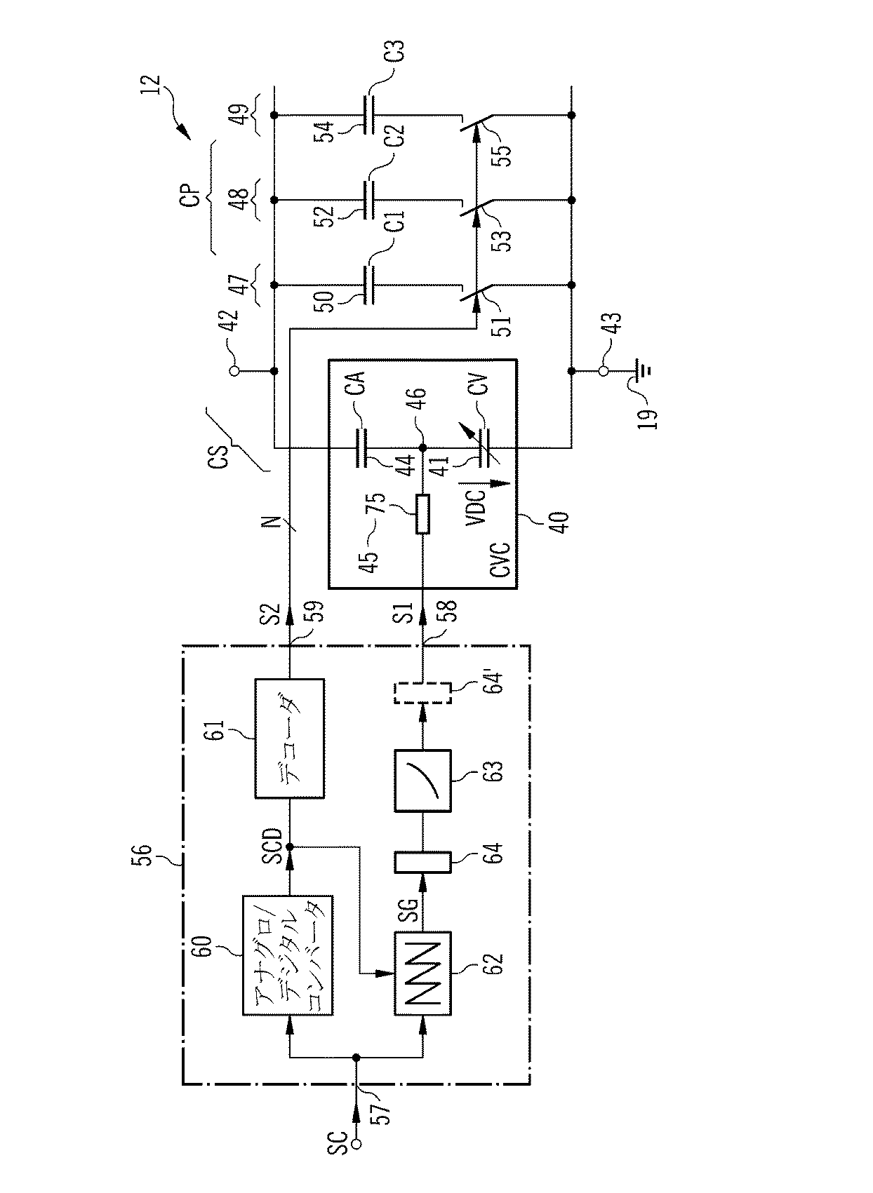
図2は、図1Aから1Dに示されているインピーダンス回路内で使用されうる例示的な第1の容量性装置を示している。図1Aから1Dの第2の容量性装置13は、図2に示されている第1の容量性装置12のようなものとして実装することもできる。第1の容量性装置12は、バラクタ41を有するバラクタ回路40を備える。バラクタ回路40の阻止コンデンサ44は、バラクタ41に直列に接続される。バラクタ41および阻止コンデンサ44の直列回路は、第1の端子42と第2の端子43との間に配置される。阻止コンデンサ44は、第1の端子42に接続される。バラクタ41は、第2の端子43に接続される。バラクタ回路40は、バラクタ41と阻止コンデンサ44とを備える容量性分圧器として実現される。バラクタ回路40は、バイアス回路45を備える。バイアス回路45は、抵抗器75を有する。バイアス回路45の出力は、阻止コンデンサ44とバラクタ41との間のバラクタノード46に接続される。
FIG. 2 shows an exemplary first capacitive device that may be used in the impedance circuit shown in FIGS. 1A-1D. The
さらに、第1の容量性装置12は、少なくとも1つの直列回路47から49を備える。バラクタ回路40は、少なくとも1つの直列回路47から49に並列に接続される。第1、第2、および第3の直列回路47から49は、第1の端子42を第2の端子43に接続する。第1、第2、および第3の直列回路47から49は、並列分岐を形成する。第1の直列回路47は、第1の分岐である。第1の直列回路47は、直列に配置されている第1のコンデンサ50および第1のスイッチ51を備える。第2の直列回路48および第3の直列回路49は第1の直列回路47のようなものとして実装される。第2の直列回路48は、第2のコンデンサ52および第2のスイッチ53を備える。これに対応して、第3の直列回路49は、第3のコンデンサ54および第3のスイッチ55を備える。第2の直列回路48および第3の直列回路49は、第2の分岐および第3の分岐を形成する。第1のコンデンサ50、第2のコンデンサ52、および第3のコンデンサ54は、それぞれ、第1の容量値C1、第2の容量値C2、および第3の容量値C3を有する。第1の容量性装置12は、個数Nの直列回路47から49の並列回路を備える。数Nは、1以上の任意の数とすることができる。N番目の直列回路のコンデンサの容量値CNは、式(1)
Furthermore, the
![]()
![]()
に従って計算することができ、ただし、第1の容量値C1は、直列回路47から49のコンデンサ50、52、54のうちの最小の容量値である。そして、2進符号化が、第1の容量性装置12内に実装される。最小の容量値C1は、最下位ビット容量値と称することもできる。少なくとも1つの直列回路47から49の並列回路は、スイッチャブルコンデンサバンクまたはスイッチトコンデンサアレイとして表すこともできる。
However, the first capacitance value C1 is the smallest capacitance value among the
さらに、第1の容量性装置12は、制御回路56を備える。制御回路56は、入力57とバラクタ回路40に接続されている第1の出力58とを有する。第1の出力58は、バイアス回路45を介してバラクタノード46に接続される。制御回路56の第2の出力59は、第1のスイッチ51、第2のスイッチ53、および第3のスイッチ55の制御端子に接続される。第2の出力59は、並列バス端子として実装される。制御回路56は、入力57を第2の出力59に接続するアナログ/デジタルコンバータ60、略してADコンバータを備える。そして、ADコンバータ60は、入力57と少なくとも1つの直列回路47から49のスイッチ51、53、55の制御端子との間に配置される。ADコンバータ60は、完全フラッシュコンバータとすることができる。制御回路56のデコーダ61は、ADコンバータ60の出力を第2の出力59に接続する。さらに、制御回路56は発生器62を備える。入力57は、発生器62を介して第1の出力58に接続される。発生器62は、その入力側でADコンバータ60の出力にも接続される。制御回路56の波形整形回路63は、発生器62の出力を第1の出力58に接続する。さらに、制御回路56は、発生器62の出力に接続されている誤り訂正回路64を備える。こうして、誤り訂正回路64は、発生器62を波形整形回路63に結合する。
Further, the
第1の容量性装置12を制御するために、制御信号SCが制御回路56の入力57に供給される。制御信号SCは、アナログ信号として実装される。これは、電圧として実現され、所定の電圧範囲を有する。第1の信号S1および第2の信号S2は、制御信号SCに応じて制御回路56によって発生する。制御信号SCは、第1の容量性装置12の所定の容量値CSの一次関数である。制御信号SCは、デジタル制御信号SCDを発生するADコンバータ60に印加される。デジタル制御信号SCDは、デコーダ61を介してスイッチ51、53、55に供給される。第1のコンデンサ49、第2のコンデンサ51、および第3のコンデンサ53の容量値C1、C2、C3が、式(1)に従って設計されている場合、デコーダ61は、ADコンバータ60の出力をスイッチ51、53、55の制御端子に接続するラインのみを備える。ADコンバータ60の出力は、並列バスの端子として実現される。
In order to control the
発生器62は、制御信号SCに依存する発生器信号SGおよび少なくとも1つの直列回路47から49によって与えられる所望の容量値CPを供給する。発生器62は、鋸歯状波発生器として実装することができる。発生器信号SGは、アナログ信号である。発生器信号SGは、第1の容量性装置12の所定の容量値CSと少なくとも1つの直列回路47から49の現在の容量値CPとの間の差に依存する。そのため、発生器信号SGは、バラクタ回路40によって供給されなければならない容量値CVCに関する情報を含む。第1の容量性装置12の容量値CSは、バラクタ回路40の容量値CVCと少なくとも1つの直列回路47から49の容量値CPとの和である、つまり、CS=CVC+CPである。そのため、発生器信号SGは、バラクタ回路40の容量値CVCの所定の値の一次関数である。第1の信号S1および第2の信号S2は、バラクタ回路40の容量値CVCと少なくとも1つの直列回路47から49の容量値CPとの和が第1の容量性装置12の所定の容量値CSに等しくなるように供給される。
The
バラクタ回路40の容量値CVCは、第1の信号S1に非線形的な形で依存するので、波形整形回路73は、第1の信号S1が発生器信号SGの非線形関数となるように第1の信号S1を供給する。誤り訂正回路64は、バラクタ回路40の容量値CVCを較正するように設計されている。誤り訂正回路64は、バラクタ回路40の容量値CVCの範囲が第1のコンデンサ50の容量値C1に等しくなるように実現される。誤り訂正回路64は、リアルタイムで反応する。誤り訂正回路64は、ソフトウェアテーブルを備えることができる。ソフトウェアテーブルは、インピーダンス回路10を備えるシステムによって較正手順に従い制御される。
Since the capacitance value CVC of the
第1の信号S1は、第1の出力58を介してバラクタ回路40に印加される。第1の信号S1は、バラクタ回路40の容量値CVCを制御する。第1の信号S1は、アナログ信号である。第1の信号S1は、電圧として実現される。第1の信号S1により、バラクタ41にかかるバラクタ電圧VDCが設定され、したがって、バラクタ41の容量値CVが制御される。バイアス回路45は、バラクタノード46での高周波電圧が第1の出力58に印加されることを阻止する。容量値CAを有する阻止コンデンサ44は、DC電流がバラクタ回路40内を流れるのを阻止する。
The
第2の信号S2は、第2の出力59を介して第1のスイッチ51、第2のスイッチ53、および第3のスイッチ55の制御端子に供給される。第2の信号S2は、デジタル並列バス信号として実装される。第2の信号S2は、少なくとも1つの直列回路47から49の並列回路の容量値CPのデジタル制御を行う。第1の動作状態において、第2の信号S2は、第1のスイッチ51を導通状態に設定する。したがって、第1の直列回路47は、第1の容量値C1を取得する。第2の動作状態において、第1のスイッチ51は、非導通状態に設定される。そのため、第1の直列回路47の容量値は、ほぼゼロである。第2の信号S2は、少なくとも1つの直列回路47から49のコンデンサ50、52、54のうちのどれが第1の容量性装置12の容量値CSに寄与するかを制御する。
The second signal S2 is supplied to the control terminals of the
第1の容量性装置12のバラクタ41およびコンデンサ44、50、52、54は、半導体技術または微小電気機械システム技術によって製造することができる。スイッチ51、53、55は、電界効果トランジスタとして実現される。インピーダンス回路10は、シングルチップとして、またはマルチチップとして実現されうる。マルチチップの場合、スイッチャブルコンデンサ50、52、54およびバラクタ41は、ハイブリッド技術によって集積化される。インピーダンス回路10は、有利には、アナログ回路によって制御される。したがって、精巧なデジタル制御は不要である。
The
第1の容量性装置12は、有利には、第1の容量性装置12が最小容量値CMINと最大容量値CMAXとの間の所定の容量範囲から外れた容量値CSを有するように制御される。有利には、第1の容量性装置12の容量値CSの単調制御が達成されうる。導関数dC/dV、つまり、d CS/d SCは、制御信号SCの全範囲にわたって正であるか、または負であるかのいずれかである。第1の容量性装置12は、高いクオリティファクタを示す。クオリティファクタは、第1の容量性装置12のインピーダンスの虚部とインピーダンスの抵抗部との比である。クオリティファクタが高ければ、その結果、整合回路網の挿入損失が低くなる。さらに、第1の容量性装置12は、低い歪みを示す。数Nが大きくなると、歪みは小さくなる。数Nは、インピーダンス回路10の複雑度とインピーダンス回路10によって引き起こされる歪みとの間に適切なトレードオフの関係を見つけられるように選択されうる。
The
一代替的実施形態では、第1のコンデンサ50、第2のコンデンサ52、および第3のコンデンサ54の容量値C1、C2、C3は、式(1)に従って実現されない。そのため、デコーダ61は、論理ゲートを備える。デコーダ61は、グレイ符号化または温度計符号化を行うように実装することができる。グレイ符号化または温度計符号化では、ある時点において第1のスイッチ51、第2のスイッチ53、および第3のスイッチ55のうちの1つのスイッチだけが作動する。2進符号化、グレイ符号化、または温度計符号化を混合したものも使用することができる。
In an alternative embodiment, the capacitance values C1, C2, C3 of the
一代替的実施形態では、誤り訂正回路64は、波形整形回路63の出力に接続される。位置は、破線で示されている。
In an alternative embodiment,
一代替的実施形態では、バイアス回路45は、ダイオード、トランジスタ、抵抗器75、およびチョークインダクタなどのインダクタを有する群の少なくとも1つの素子を備える。
In one alternative embodiment, the
図3Aから3Dは、図2に示されているバラクタ回路のさらなる実施形態であり、図2の第1の容量性装置および第2の容量性装置において使用されうる、例示的なバラクタ回路を示している。図3Aによれば、バラクタ41は、バラクタノード43でのDC電圧によりバラクタ41内をDC電流が通らない向きに配置される。バラクタ41のカソードは、バラクタノード46に接続される。バラクタ電圧VDCが正である場合、DC電流は、バラクタノード46から阻止コンデンサ44を通って流れることも、またバラクタ41を通って流れることもありえない。そのため、バラクタ41は、エネルギーを節約できるように制御されうる。
3A through 3D are further embodiments of the varactor circuit shown in FIG. 2 and illustrate exemplary varactor circuits that may be used in the first capacitive device and the second capacitive device of FIG. ing. According to FIG. 3A, the
図3Bのバラクタ回路40’において、阻止コンデンサ44は、第2のバラクタ70として実装される。第2のバラクタ70およびバラクタ41は、DC電流がバラクタ41と第2のバラクタ70との直列回路を通って流れることができない向きに配置される。さらに、バラクタ41および第2のバラクタ70は、バラクタノード46にDC電位が生じることでDC電流がバラクタ41を通ることも、また第2のバラクタ70を通ることもない向きに配置される。バラクタ41と第2のバラクタ70との直列回路により、バラクタ回路40’の特性は、図3Aのバラクタ回路40の特性と比較してより線形性が高い。さらに、バラクタ回路40’は、直列に接続されている第3のバラクタ71および第4のバラクタ72を備える。第3のバラクタ71と第4のバラクタ72との直列回路は、バラクタ41と第2のバラクタ70との直列回路に並列に接続される。これら2つの直列回路の並列接続は、バラクタ回路40’の容量値CVCを増大させる。第1の出力58は、さらなるバイアス回路73を介してさらなるバラクタノード74に接続される。
In the
図3Cによれば、バイアス回路45は、第1のバイアスバラクタ76と第2のバイアスバラクタ77との並列回路を備える。バイアスバラクタ76、77の並列回路は、抵抗器75に直列に接続される。第1のバイアスバラクタ76のアノードは、第2のバイアスバラクタ77のカソードに接続される。第2のバイアスバラクタ77のアノードは、第1のバイアスバラクタ76のカソードに接続される。逆並列バラクタペア76、77により、バイアス回路45の高いインピーダンスが得られる。そのため、バラクタ電圧VDCを発生するためのエネルギー消費量は低い。
According to FIG. 3C, the
図3Dのバラクタ回路40’’’は、少なくとも3つのバラクタ41、70、71を備える。図3Bから3Dのバラクタ回路は、複数のバラクタを備える。そのため、バラクタ回路40によって引き起こされる歪みは、キャンセル効果によって低減される。
The
図4Aは、バラクタ41の例示的な特性を示している。バラクタ41の容量値CVは、バラクタ41のアノードとカソードとの間のDC電圧であるバラクタ電圧VDCに依存するように示されている。容量値CVは、バラクタ電圧VDCが増加すると減少する。バラクタ41は、第1のバラクタ電圧V1で第1の容量値CV1を有し、第2のバラクタ電圧V2で第2の容量値CV2を有する。第2の電圧V2は、バラクタ41に印加される最低電圧であるものとしてよい。第1の電圧V1は、バラクタ41に供給される最高電圧であるものとしてよい。容量値CVは、式(2)
FIG. 4A shows exemplary characteristics of the
によるバラクタ電圧VDCに依存し、式(2)中、K、phi、m、およびC0はフィッティングパラメータである。阻止コンデンサ44は、バラクタ41に直列に接続されているので、バラクタ電圧VDCは、インピーダンス回路10から取り除かれる。バラクタ回路40の第1の容量値CVC1は、バラクタ41の第1の容量値CV1および阻止コンデンサ44の容量値CAに依存する。同様に、バラクタ回路40の第2の容量値CVC2は、第2の容量値CV2および容量値CAに依存する。値CVC1およびCVC2は、式(3),(4)
Depending on the varactor voltage VDC, K, phi, m, and C0 are fitting parameters in equation (2). Since the blocking
に従って計算することができる。 Can be calculated according to:
バラクタ41、したがってバラクタ回路40は、連続する範囲の容量値を取得することができる。バラクタ41および阻止コンデンサ44の直列回路は、バラクタ回路40の非線形性を低減する。容量値VCとバラクタ電圧VDCとの間の関係が非線形であるため、高調波歪みを発生しうる。バラクタ41および阻止コンデンサ43を備えるコンデンサデバイダにより、第1の端子42と第2の端子43との間の高周波電圧振幅全体のわずかな部分のみがバラクタ41上で利用可能であることが保証される。歪みは、バラクタ41にかかる高周波交流電圧の結果生じうるものであり、バラクタ41を通る交流電流の関数とはならないことがある。バラクタ41によって引き起こされる歪みの効果が低減されるが、それは、バラクタ41が阻止コンデンサ44を使ってインピーダンス回路10に弱くしか結合されず、バラクタ41にかかる電圧の振幅が小さいからである。
The
図4Bは、第1の容量性装置の容量値の例示的な特性を示している。バラクタ回路40の容量値CVC、少なくとも1つの直列回路47から49の並列回路の容量値CP、および第1の容量性装置12の容量値CSは、制御信号SCに依存する。容量値CPは、制御信号SCに応じて段階的に増大する。容量値CPは、階段の形態を有する。1つの段の高さは、第1の容量値C1に等しい。段の数は、少なくとも1つの直列回路47から49の個数Nに依存する。容量値CPの最大値CPMAXは、すべてのスイッチ51、53、55が導通状態にある場合に得られる。そのため、第1の容量性装置12の最小容量値CMINは、バラクタ回路40の容量値CVC1であるが、最大容量値CMAXは、値CPMAXと容量値CVC2との和である。容量値CSは、制御信号SCに一次比例する。容量値CSの特性には、ほぼ段はない。
FIG. 4B shows exemplary characteristics of the capacitance value of the first capacitive device. The capacitance value CVC of the
バラクタ41によって引き起こされる高調波および相互変調の歪みの影響は、阻止コンデンサ44と少なくとも1つの直列回路47から49の並列回路とによって低減される。さらに、第1の容量性装置12は、高いクオリティファクタを取得する。インピーダンス回路10の容量値の粗調整は、スイッチャブルコンデンサ50、52、54を使って実行され、微調整は、弱く結合されたバラクタ41によって実行される。容量値CSの全変動は、リニアブロックの容量値CVCの変動とスイッチャブルブロックの容量値CPの変動の和である。
The effects of harmonic and intermodulation distortion caused by the
バラクタ回路40を使って調整できる容量値範囲は、少なくとも1つの直列回路47から49の並列回路の容量値CPの段のそれぞれに等しいか、または高い。これらの段は、第1の容量値C1に等しい。第1の信号S1の鋸歯状波の電圧範囲は、バラクタ回路40の容量値CVCを、少なくとも1つの直列回路47から49の並列回路が変えることができるような同じ最小容量値に正確に変えるように選択される。
The capacitance value range that can be adjusted using the
図5は、図1Aから1Dのインピーダンス回路を使用することができる例示的な通信回路を示している。通信回路130は、電力増幅器131、インピーダンス回路10、およびアンテナ132を備える。インピーダンス回路10は、電力増幅器131の出力をアンテナ132に接続する。インピーダンス回路10は、電力増幅器131とアンテナ132との間に整合回路網として実装される。インピーダンス回路10は、例えばモバイル通信用の高周波回路内に使用される。
FIG. 5 shows an exemplary communication circuit that can use the impedance circuit of FIGS. 1A-1D. The
雑音電界強度に関するモバイル通信用のデバイスの要件は、インピーダンス回路10によって満たすことができる。インピーダンス回路10は、さまざまな動作状態の下で電力増幅器131とアンテナ132との間の低損失インピーダンス変換を行う。インピーダンス回路10は、電力増幅器131とアンテナ132との不整合を補償し、モバイル通信用のデバイスの放射効率を高める。
The device requirements for mobile communication with respect to the noise field strength can be met by the
図6Aは、制御回路56の詳細の例示的な実施形態を示している。ADコンバータ60は、少なくとも1つのコンパレータ81を備える。図6AのADコンバータ60は、並列コンバータとして設計される。ADコンバータ60は、第1、第2、および第3のコンパレータ81から83を備える。第1、第2、および第3のコンパレータ81から83のうちのそれぞれのコンパレータの入力接続部は、制御回路56の入力57に接続される。第1の基準源84は、第1のコンパレータ81の第2の入力端子に接続される。それに対応して、第2の基準源85は、第2のコンパレータ82の第2の入力に接続される。第3の基準源86は、第3のコンパレータ83の第2の入力に接続される。第1の基準電圧源84、第2の基準電圧源85、および第3の基準電圧源86は、少なくとも3つのノードを持つ分圧器によって実装することができる。コンパレータ81から83の出力は、ADコンバータ60の出力を形成する。デコーダ61は、ADコンバータ60の出力に接続される。第1のコンデンサ50、第2のコンデンサ52、および第3のコンデンサ54の容量値C1、C2、C3が式(1)に従う場合、デコーダ61は、デジタル回路を備える。
FIG. 6A shows an exemplary embodiment of the details of the
発生器62は、総和ユニット88および減算ユニット89を備える。総和ユニット88は、その入力側で第1、第2、および第3のコンパレータ81から83の出力端子に接続される。減算ユニット89の第1の入力は、入力57に接続される。減算ユニット89の第2の入力は、総和ユニット88の出力に接続される。減算ユニット89の出力は、発生器62の出力を形成し、第1の出力58に接続される。バッファ90は、入力57を減算ユニット89の第1の入力端子に接続する。
The
第1の基準源84は、第1の基準電圧VR1を第1のコンパレータ81の第2の入力に供給する。同様に、第2の基準源85は、第2の基準電圧VR2を第2のコンパレータ82に供給し、第3の基準源86は、第3のコンパレータ83に印加する第3の基準電圧VR3を発生する。第1の基準電圧VR1、第2の基準電圧VR2、および第3の基準電圧VR3を、分圧器のノードから取り出すことができる。第1の基準電圧VR1は、第2の基準電圧VR2より小さく、第2の基準電圧VR2は、第3の基準電圧VR3より小さい。後の2つの基準電圧の差は、第1の基準電圧VR1に等しい。この差は、第1のコンデンサ50の第1の容量値C1に対応する。3つのコンパレータ81から83は、制御信号SCをそれらの対応する基準電圧VR1、VR2、VR3と比較し、第1のコンパレータ信号SC1、第2のコンパレータ信号SC2、および第3のコンパレータ信号SC3を発生させる。デジタル制御信号SCDは、第1のコンパレータ信号SC1、第2のコンパレータ信号SC2、および第3のコンパレータ信号SC3を含む。
The
総和ユニット88は、第1のコンパレータ信号SC1、第2のコンパレータ信号SC2、および第3のコンパレータ信号SC3を受信する。第1のコンパレータ信号SC1、第2のコンパレータ信号SC2、および第3のコンパレータ信号SC3は、制御信号SCが対応する基準電圧VR1、VR2、VR3より大きいことを示している。総和回路88は、第1のコンパレータ信号SC1、第2のコンパレータ信号SC2、および第3のコンパレータ信号SC3を加算する。総和回路88は、コンパレータ出力信号SC1、SC2、SC3の論理値を加算する。論理値が1であるコンパレータ出力信号は、第1の基準電圧VR1の電圧値を有する。総和ユニット88から出力される総和電圧VSUMは、論理値1が出力されているコンパレータの数に第1の基準電圧VR1を掛けた値に等しい。総和電圧VSUMは、現在の制御信号SCより小さい最高基準電圧VR1、VR2、VR3に等しい。減算ユニット89は、制御信号SCと総和信号VSUMとの差である発生器信号SGを発生させる。図6Aに示されているように、総和信号VSUMは、制御信号SCの階段関数であり、制御信号SCが大きくなると、発生器信号SGは鋸歯状になる。
Summing
一代替的実施形態では、第1のコンデンサ49、第2のコンデンサ51、および第3のコンデンサ53の容量値C1、C2、C3は、等しい。その場合、デコーダ61は、第1、第2、および第3のコンパレータ81から83を第1のスイッチ51、第2のスイッチ53、および第3のスイッチ55の制御端子に接続する接続線を備えるだけである。第1のコンパレータ81の出力は、第1のスイッチ84の制御端子に接続される。例えば、制御信号SCの値が第1の基準電圧VR1より大きい場合、第1のコンパレータ信号SC1は、第1のスイッチ84を導通状態に設定する。
In an alternative embodiment, the capacitance values C1, C2, C3 of the
図6Bは、制御回路56の詳細の代替的な実施形態を示している。図6Aおよび6Bの制御回路56は、図2に示されている第1の容量性装置で使用することができる。ADコンバータ60は、パイプラインコンバータとして実現される。ADコンバータ60は、少なくとも1つの副回路94を備える。第1の副回路94は、第1のコンパレータ96および第1の減算ユニット97を備える。第1のコンパレータ96の第1の入力および減算ユニット97の第1の入力は、入力57に接続される。第1のコンパレータ96の第2の入力は、基準電圧源95に接続される。第1の減算ユニット97の第2の入力は、第1のコンパレータ96の出力に接続される。第1のバッファ98は、入力57を第1の減算ユニット97の第1の入力に接続する。
FIG. 6B shows an alternative embodiment of the details of the
第2の副回路99は、第2のコンパレータ100および第2の減算ユニット101を備える。さらに、これは、第2のバッファ102を備える。第2の副回路99の回路構造は、第1の副回路94の回路構造に対応する。しかし、第2のコンパレータ100の第1の入力および第2の減算ユニット101の第1の入力は、第1の減算ユニット97の出力に接続される。第1のコンパレータ96および第2のコンパレータ100の出力端子は、ADコンバータ60の出力を形成する。図6Aのデコーダ61も、図6Bの制御回路56内で使用することができる。第2の減算ユニット101の出力は、第2の副回路99の出力を形成し、発生器62の出力に接続される。そのため、図6BのADコンバータ60は、発生器62も組み込む。
The
基準電圧源95は、基準電圧VREFを発生させる。基準電圧VREFは、第1の容量値C1に対応する。基準電圧VREFは、第1のコンパレータ96の第2の入力および第2のコンパレータ100の第2の入力に印加される。制御信号SCは、第1の減算ユニット97の第1の入力および第1のコンパレータ96の第1の入力に供給される。
The
第1のコンパレータ96の出力での第1のコンパレータ信号SC1は、制御電圧SCと基準電圧VREFとの比較結果に依存する。制御電圧SCが、基準電圧VREFより高い場合、第1のコンパレータ信号SC1は、論理値1と基準電圧VREFに等しい電圧とを有する。この時点において、第1の減算ユニット97の出力での出力電圧は、制御信号SCから基準電圧VREFを引いた結果に等しい。しかし、制御電圧SCが、基準電圧VREFより小さい場合、第1のコンパレータ信号SC1は、論理値0を有し、0Vの電圧が第1の減算ユニット97の第2の入力に印加される。第1の減算ユニット97での出力電圧は、この時点の制御信号SCに等しい。
The first comparator signal SC1 at the output of the
第1の減算ユニット97の出力電圧は、第2の副回路99の入力を介して第2のコンパレータ100の第1の入力および第2の減算ユニット101の第1の入力に供給される。第2の減算ユニット101の出力電圧は、第1の減算ユニット97の出力信号が基準電圧VREFより大きい場合、つまり、現在の制御信号SCが基準電圧VREFの2倍以上である場合に、制御信号SCから基準電圧VREFの2倍を差し引いた電圧である。ADコンバータ60は、第1の副回路94および第2の副回路99の構造を有するさらなる副回路を少なくとも備えることができる。それぞれの後の副回路は、入力信号が基準電圧VREFより高い場合に、基準電圧VREFだけ入力信号を低減する。基準電圧VREFで制御信号SCをその後低減することによって、ADコンバータ60はデジタル制御信号SCDを決定する。図6Bの場合の第2の副回路99である最後の副回路の最後の減算ユニットの出力端子に出る信号は、発生器信号SGに等しい。
The output voltage of the
制御信号SCが高くなると、有利には第1のコンパレータ信号SC1、第2のコンパレータ信号SC2、および第3のコンパレータ信号SC3のうちの1つだけが、図6Aおよび6Bの制御回路56においてある時点に変更される。
When the control signal SC goes high, preferably only one of the first comparator signal SC1, the second comparator signal SC2, and the third comparator signal SC3 is at a certain point in the
図7は、図2の制御回路で使用することができる例示的な誤り訂正回路を示している。誤り訂正回路64は、バラクタ回路40に接続される。誤り訂正回路64は、増幅器110および第1の基準コンデンサ111を備える。バラクタノード46は、増幅器100の第1の入力に接続される。第1の基準コンデンサ111は、増幅器100の第2の入力を第2の端子43に接続する。第2の基準コンデンサ112は、バラクタ回路40に直列に接続される。それに対応して、第3の基準コンデンサ113は、第1の基準コンデンサ111に直列に接続される。バラクタ40と第2の基準コンデンサ112の直列回路、さらには第1の基準コンデンサ111と第3の基準コンデンサ113の直列回路は、入力ノード114と第2の端子43との間で並列に接続される。そのため、バラクタ回路40および第1、第2、および第3の基準コンデンサ111から113は、容量性ブリッジ構成で接続される。第1の基準コンデンサ111、第2の基準コンデンサ112、および第3の基準コンデンサ113の容量値は、等しい。そこで、バラクタ41は、増幅器100の第1の入力を第2の端子43に接続する。増幅器110の第1の入力は、第2の基準コンデンサ112と阻止コンデンサ44とを介して入力ノード114に接続される。
FIG. 7 shows an exemplary error correction circuit that can be used in the control circuit of FIG. The
さらに、発振器115は、入力ノード114に接続された出力を有する。緩衝増幅器116は、発振器115と入力ノード114との間に配置される。増幅器100の出力は、整流器117の入力に接続される。整流器117は、整流ダイオード118、整流コンデンサ119、および整流抵抗器120を備える。整流器117の入力は、整流ダイオード118を介して整流器117の出力に接続される。整流コンデンサ119と整流抵抗器117との並列回路は、整流器117の出力を第2の端子43に接続する。ループ増幅器121は、整流器117の出力をバラクタ回路40に接続する。ループ増幅器121は、バイアス回路45を介してバラクタノード46に接続される。ループコンデンサ122は、ループ増幅器121に接続される。
In addition,
発振器115は、緩衝増幅器116を介して入力ノード114に印加される発振器信号VOSCを発生させる。そのため、発振器信号VOSCは、バラクタ回路40および第2の基準コンデンサ112を備えるブリッジの第1の経路に、また第1の基準コンデンサ111および第3の基準コンデンサ113を備えるブリッジの第2の経路に供給される。増幅器110は、第1の基準コンデンサ111にかかる電圧をバラクタ回路40によって発生する電圧と比較する。増幅器100の出力信号は、第1の基準コンデンサ111にかかる電圧とバラクタノード46での電圧との差に依存する。増幅器110の出力信号は、整流器117によって整流され、バラクタ回路40にフィードバックされる。整流器117の出力信号は、ループ増幅器121によって増幅され、バイアス回路45に第1の信号S1として印加される。
The
増幅器100の2つの入力端子における信号同士の差が存在する場合、第1の信号S1は、増幅器100の入力間の差がほぼゼロになるまで変化する。誤り訂正回路64の利点は、バラクタ41の最大容量値が第1の基準コンデンサ111の容量値に等しくなるように第1の信号S1の値を決定することができる点である。誤り訂正回路64は、自己較正を実行することができる。誤り訂正回路64は、インピーダンス回路10を備えるシステムでは見えないように設計される。誤り訂正回路64の支配極は、較正がインピーダンス回路10を備えるシステムに影響を及ぼさないように十分高いものとなるように選択される。
If there is a difference between the signals at the two input terminals of the
図示されていない一代替的実施形態では、インピーダンス回路10を備えるシステム内で取り出せる高周波電圧のわずかな部分が較正目的に使用され、発振器115は省かれる。インピーダンス回路10が通信回路の一部である場合、電力増幅器131の内部電圧を基準電圧VOSCとして使用することができる。
In an alternative embodiment, not shown, a small portion of the high-frequency voltage that can be taken out in the system comprising the
破線で示されている一代替的実施形態では、増幅器110の第1の入力は、バラクタ回路40と第2の基準コンデンサ112との間のノードに接続される。そこで、バラクタ回路40の容量値CVCを第1の基準コンデンサ111の容量値と比較する。第1の基準コンデンサ111の容量値は、第1の容量値C1に等しくてもよい。
In an alternative embodiment, shown in dashed lines, the first input of
図8Aから8Dは、第1の容量性装置12のシミュレーション結果を示している。これらの信号は時間tに対して示されている。制御信号SCは、100Hzの周波数を持つ正弦波である。図8Aは、少なくとも1つの直列回路によってもたらされる容量値CPを示している。図8Bは、鋸歯状の形を有する発生器信号SGを例示している。図8Cは、第1の容量性装置12の容量値CSを示している。図8Dは、図8Cに示されている容量値CSの時間導関数を例示している。図8Cに示されている容量値CSおよび図8Dに示されている導関数は連続であり、正弦波の形を有するので、バラクタ回路40と少なくとも1つの直列回路47から49との整合が非常によいことが実証される。
8A to 8D show the simulation results of the
図9Aから9Dは、第1の容量性装置12の異なるコンデンサの容量値の2.5%の不整合について得られた例示的なシミュレーション結果を示している。この不整合の結果、スパイクが発生するが、これは図9Dを見るとわかる。スパイクは、適切に設計されうる有限の長さを持つので、送信器または受信チャネル内のノイズなどのスペクトル汚染をシステム限界の範囲内に十分留めることができる。図9Aから9Dに示されている場合でもある、その結果得られる信号の導関数が、正しい符号を依然として有している限り、第1の容量性装置12は、制御ループの一部として使用することができる。
FIGS. 9A through 9D show exemplary simulation results obtained for a 2.5% mismatch in the capacitance values of the different capacitors of the
C1 第1の容量値
C2 第2の容量値
C3 第3の容量値
CA、CP、CS、CV、CVC 容量値
CMAX 最大容量値
CMIN 最小容量値
CV1、CVC1 第1の容量値
CV2、CVC2 第1の容量値
S1 第1の信号
S2 第2の信号
SC 制御信号
SC1 第1のコンパレータ信号
SC2 第2のコンパレータ信号
SC3 第3のコンパレータ信号
SCD デジタル制御信号
SG 発生器信号
SIN 入力信号
SOUT 出力信号
t 時間
V1 第1のバラクタ電圧
V2 第2のバラクタ電圧
VDC バラクタ電圧
VOSC 発振器信号
VR1 第1の基準電圧
VR2 第2の基準電圧
VR3 第3の基準電圧
VREF 基準電圧
VSUM 総和信号
10、10’、10’’ インピーダンス回路
11 入力端子
12 第1の容量性装置
13 第2の容量性装置
14 出力端子
15 追加のコンデンサ
16 受動コンポーネント
17 デルタ回路網
18 さらなるノード
19 基準電位端子
20 インダクタ
21 星型回路網
22 中心ノード
23 さらなる容量性装置
24、25 さらなる受動コンポーネント
26、27 さらなる入力端子
28、29 さらなる出力端子
40、40’、40’’ バラクタ回路
41 バラクタ
42 第1の端子
43 第2の端子
44 阻止コンデンサ
45 バイアス回路
46 バラクタノード
47 第1の直列回路
48 第2の直列回路
49 第3の直列回路
50 第1のコンデンサ
51 第1のスイッチ
52 第2のコンデンサ
53 第2のスイッチ
54 第3のコンデンサ
55 第3のスイッチ
56 制御回路
57 入力
58 第1の出力
59 第2の出力
60 アナログ/デジタルコンバータ
61 デコーダ
62 発生器
63 波形整形回路
64 誤り訂正回路
70 第2のバラクタ
71 第3のバラクタ
72 第4のバラクタ
73 さらなるバイアス回路
74 さらなるバラクタノード
75 抵抗器
76 第1のバイアスバラクタ
77 第2のバイアスバラクタ
81 第1のコンパレータ
82 第2のコンパレータ
83 第3のコンパレータ
84 第1の基準源
85 第2の基準源
86 第3の基準源
88 総和ユニット
89 減算ユニット
90 バッファ
94 第1の副回路
95 基準電圧源
96 第1のコンパレータ
97 第1の減算ユニット
98 第1のバッファ
99 第2の副回路
100 第2のコンパレータ
101 第2の減算ユニット
102 第2のバッファ
110 増幅器
111 第1の基準コンデンサ
112 第2の基準コンデンサ
113 第3の基準コンデンサ
114 入力ノード
115 発振器
116 緩衝増幅器
117 整流器
118 整流ダイオード
119 整流コンデンサ
120 整流抵抗器
121 ループ増幅器
122 ループコンデンサ
130 通信回路
131 電力増幅器
132 アンテナ
C1 first capacitance value C2 second capacitance value C3 third capacitance value CA, CP, CS, CV, CVC capacitance value CMAX maximum capacitance value CMIN minimum capacitance value CV1, CVC1 first capacitance value CV2, CVC2 first Capacitance value S1 first signal S2 second signal SC control signal SC1 first comparator signal SC2 second comparator signal SC3 third comparator signal SCD digital control signal SG generator signal SIN input signal SOUT output signal t time V1 first varactor voltage V2 second varactor voltage VDC varactor voltage VOSC oscillator signal VR1 first reference voltage VR2 second reference voltage VR3 third reference voltage VREF reference voltage VSUM sum signal 10, 10 ', 10'' Impedance circuit 11 Input terminal 12 First capacitive device 13 Second capacitive device 14 Output terminal 5 Additional capacitor 16 Passive component 17 Delta network 18 Additional node 19 Reference potential terminal 20 Inductor 21 Star network 22 Central node 23 Additional capacitive device 24, 25 Additional passive component 26, 27 Additional input terminals 28, 29 Further output Terminal 40, 40 ', 40''Varactor circuit 41 Varactor 42 First terminal 43 Second terminal 44 Blocking capacitor 45 Bias circuit 46 Varactor node 47 First series circuit 48 Second series circuit 49 Third series circuit 50 first capacitor 51 first switch 52 second capacitor 53 second switch 54 third capacitor 55 third switch 56 control circuit 57 input 58 first output 59 second output 60 analog / digital converter 61 Decoder 62 Generator 63 Wave Shaping circuit 64 Error correction circuit 70 Second varactor 71 Third varactor 72 Fourth varactor 73 Further bias circuit 74 Further varactor node 75 Resistor 76 First bias varactor 77 Second bias varactor 81 First comparator 82 Second comparator 83 Third comparator 84 First reference source 85 Second reference source 86 Third reference source 88 Summing unit 89 Subtraction unit 90 Buffer 94 First subcircuit 95 Reference voltage source 96 First comparator 97 first subtraction unit 98 first buffer 99 second sub circuit 100 second comparator 101 second subtraction unit 102 second buffer 110 amplifier 111 first reference capacitor 112 second reference capacitor 113 third Reference capacitor 114 input node 115 oscillator 1 16 Buffer amplifier 117 Rectifier 118 Rectifier diode 119 Rectifier capacitor 120 Rectifier resistor 121 Loop amplifier 122 Loop capacitor 130 Communication circuit 131 Power amplifier 132 Antenna
Claims (11)
バラクタ(41)を有するバラクタ回路(40)および少なくとも1つの直列回路(47、48、49)を備える第1の容量性装置(12)であって、
前記少なくとも1つの直列回路(47、48、49)が、直列接続されたコンデンサ(50、52、54)およびスイッチ(51、53、55)を備え、前記バラクタ回路(40)と並列に接続されている、第1の容量性装置(12)と、
追加のコンデンサ(15)を備える第2の容量性装置(13)と、
前記第1の容量性装置(12)および前記第2の容量性装置(13)を備える回路網(17、21)によって前記入力端子(11)に接続された出力端子(14)と、
前記少なくとも1つの直列回路(47、48、49)の前記スイッチ(51、53、55)を制御し、前記バラクタ回路(40)を制御する制御回路(56)と
を備え、前記制御回路(56)が、
制御信号(SC)を受信するための入力(57)、および
前記制御回路(56)の前記入力(57)と前記少なくとも1つの直列回路(47、48、49)の前記スイッチ(51、53、55)の制御端子との間に接続されるアナログ/デジタルコンバータ(60)を備え、
前記アナログ/デジタルコンバータ(60)は、パイプラインコンバータとして実現され、第1のコンパレータ(96)および第1の減算ユニット(97)を備える第1の副回路(94)、さらには第2のコンパレータ(100)および第2の減算ユニット(101)を備える第2の副回路(99)を具備し、これにより、前記第1のコンパレータ(96)および前記第2のコンパレータ(100)の出力端子は前記アナログ/デジタルコンバータ(60)の出力を形成し、前記アナログ/デジタルコンバータ(60)は発生器(62)を組み込み、前記発生器(62)の出力に前記第2の減算ユニット(101)の出力が接続され、前記発生器(62)は、前記第1の容量性装置(12)の所定の容量値(CS)と前記少なくとも1つの直列回路(47、48、49)の現在の容量値(CP)との間の差に依存する発生器信号(SG)を供給するようになっているか、または
前記アナログ/デジタルコンバータ(60)は、第1のコンパレータ(81)、第2のコンパレータ(82)、および第3のコンパレータ(83)を備える並列コンバータとして設計され、前記制御回路(56)は、前記制御回路(56)の前記入力(57)と前記バラクタ回路(40)との間に接続され、前記制御信号(SC)および前記少なくとも1つの直列回路(47、48、49)によってもたらされる容量値(CP)に依存する発生器信号(SG)を供給するように設計される発生器(62)を備え、前記発生器(62)は、総和ユニット(88)および減算ユニット(89)を備え、前記総和ユニット(88)はその入力側で前記第1のコンパレータ(81)、第2のコンパレータ(82)、および第3のコンパレータ(83)に接続され、前記減算ユニット(89)の第1の入力は、前記制御回路(56)の前記入力(57)に接続され、前記減算ユニット(89)の第2の入力は、前記総和ユニット(88)の出力に接続され、さらには前記減算ユニット(89)の出力は前記発生器(62)の出力を形成する、
インピーダンス回路。 An input terminal (11);
A first capacitive device (12) comprising a varactor circuit (40) having a varactor (41) and at least one series circuit (47, 48, 49),
The at least one series circuit (47, 48, 49) includes a capacitor (50, 52, 54) and a switch (51, 53, 55) connected in series, and is connected in parallel with the varactor circuit (40). A first capacitive device (12),
A second capacitive device (13) comprising an additional capacitor (15);
An output terminal (14) connected to the input terminal (11) by a network (17, 21) comprising the first capacitive device (12) and the second capacitive device (13) ;
A control circuit (56) for controlling the switches (51, 53, 55) of the at least one series circuit (47, 48, 49) and for controlling the varactor circuit (40);
The control circuit (56) comprises:
An input (57) for receiving a control signal (SC); and
An analog / digital converter connected between the input (57) of the control circuit (56) and the control terminal of the switch (51, 53, 55) of the at least one series circuit (47, 48, 49) (60)
The analog / digital converter (60) is realized as a pipeline converter, and includes a first comparator (94) including a first comparator (96) and a first subtraction unit (97), and further a second comparator. (100) and a second sub circuit (99) comprising a second subtraction unit (101), whereby the output terminals of the first comparator (96) and the second comparator (100) are The output of the analog / digital converter (60) is formed, the analog / digital converter (60) incorporates a generator (62), and the output of the generator (62) of the second subtraction unit (101). An output is connected, and the generator (62) is connected to a predetermined capacitance value (CS) of the first capacitive device (12) and the at least one series Circuit (47,48,49) if and supplies current capacitance (CP) and the generator signal dependent on the difference between the (SG), or
The analog / digital converter (60) is designed as a parallel converter comprising a first comparator (81), a second comparator (82), and a third comparator (83), and the control circuit (56) A capacitance connected between the input (57) of the control circuit (56) and the varactor circuit (40) and provided by the control signal (SC) and the at least one series circuit (47, 48, 49). A generator (62) designed to supply a generator signal (SG) dependent on a value (CP), said generator (62) comprising a summation unit (88) and a subtraction unit (89) The summation unit (88) has, on its input side, the first comparator (81), the second comparator (82), and the third comparator (83). And a first input of the subtraction unit (89) is connected to the input (57) of the control circuit (56), and a second input of the subtraction unit (89) is connected to the summation unit (88). The output of the subtraction unit (89) forms the output of the generator (62),
Impedance circuit.
追加のバラクタを有する追加のバラクタ回路と、
直列接続された前記追加のコンデンサ(15)および追加のスイッチを備え、前記追加のバラクタ回路と並列に接続された少なくとも1つの追加の直列回路と
を備える請求項1から8の1項に記載のインピーダンス回路。 The second capacitive device (13) is
An additional varactor circuit having an additional varactor;
9. The one of claims 1 to 8 , comprising at least one additional series circuit connected in parallel with the additional varactor circuit comprising the additional capacitor (15) and an additional switch connected in series. Impedance circuit.
アンテナ(132)と、
前記電力増幅器(131)の出力を前記アンテナ(132)に接続する請求項1から9の1項に記載のインピーダンス回路(10)と
を備える通信回路。 A power amplifier (131);
An antenna (132);
A communication circuit comprising the impedance circuit (10) according to one of claims 1 to 9, wherein an output of the power amplifier (131) is connected to the antenna (132).
第1の容量性装置(12)は、
バラクタ(41)を有するバラクタ回路(40)と、
直列接続されたコンデンサ(50、52、54)およびスイッチ(51、53、55)を備え、前記バラクタ回路(40)と並列に接続される、少なくとも1つの直列回路(48、48、49)とを具備し、
第2の容量性装置(13)は、追加のコンデンサ(15)を具備し、
入力信号(SIN)を、前記第1の容量性装置(12)および前記第2の容量性装置(13)を備える回路網(17、21)を有するインピーダンス回路(10)の入力端子(11)に供給するステップと、
第1の信号(S1)を前記バラクタ回路(40)に供給し、第2の信号(S2)を前記少なくとも1つの直列回路(47、48、49)に供給するステップと、
出力信号(SOUT)を、前記回路網(17、21)によって前記インピーダンス回路(10)の前記入力端子(11)に接続されている前記インピーダンス回路(10)の出力端子(14)から取り出すステップと、
前記第1の信号(S1)および前記第2の信号(S2)は、制御信号(SC)に応じて制御回路(56)によって発生し、前記制御信号(SC)は、前記制御回路(56)のアナログ/デジタルコンバータ(60)に印加され、前記アナログ/デジタルコンバータ(60)は、デコーダ(61)を介して少なくとも1つの直列回路(47、48、49)の前記スイッチ(51、53、55)に供給されるデジタル制御信号(SCD)を発生させるステップとを含み、
前記アナログ/デジタルコンバータ(60)は、発生器信号(SG)を供給する発生器(62)を組み込み、前記第1の信号(S1)は、前記発生器信号(SG)の非線形関数となっており、
前記アナログ/デジタルコンバータ(60)は、パイプラインコンバータとして実現され、第1のコンパレータ(96)および第1の減算ユニット(97)を備える第1の副回路(94)、さらには第2のコンパレータ(100)および第2の減算ユニット(101)を備える第2の副回路(99)を具備し、これにより、前記第1のコンパレータ(96)および前記第2のコンパレータ(100)の出力端子は前記アナログ/デジタルコンバータ(60)の出力を形成し、前記発生器(62)の出力に前記第2の減算ユニット(101)の出力が接続され、 または、前記アナログ/デジタルコンバータ(60)は、第1のコンパレータ(81)、第2のコンパレータ(82)、および第3のコンパレータ(83)を備える並列コンバータとして設計され、前記発生器(62)は、総和ユニット(88)および減算ユニット(89)を備え、前記総和ユニット(88)はその入力側で前記第1のコンパレータ(81)、第2のコンパレータ(82)、および第3のコンパレータ(83)の出力端子に接続され、前記減算ユニット(89)の第1の入力は、前記制御回路(56)の入力(57)に接続され、前記減算ユニット(89)の第2の入力は、前記総和ユニット(88)の出力に接続され、さらには前記減算ユニット(89)の出力は前記発生器(62)の出力を形成する、方法。 A method for signal conversion comprising:
The first capacitive device (12) is
A varactor circuit (40) having a varactor (41);
At least one series circuit (48, 48, 49) comprising a capacitor (50, 52, 54) and a switch (51, 53, 55) connected in series and connected in parallel with said varactor circuit (40); Comprising
The second capacitive device (13) comprises an additional capacitor (15),
An input signal (SIN) is input to an input terminal (11) of an impedance circuit (10) having a network (17, 21) comprising the first capacitive device (12) and the second capacitive device (13). Supplying to,
Supplying a first signal (S1) to the varactor circuit (40) and supplying a second signal (S2) to the at least one series circuit (47, 48, 49);
Extracting the output signal (SOUT) from the output terminal (14) of the impedance circuit (10) connected to the input terminal (11) of the impedance circuit (10) by the network (17, 21); ,
The first signal (S1) and the second signal (S2) are generated by a control circuit (56) in response to a control signal (SC), and the control signal (SC) is generated by the control circuit (56). The analog / digital converter (60) is applied to the switch (51, 53, 55) of the at least one series circuit (47, 48, 49) via the decoder (61). Generating a digital control signal (SCD) supplied to
The analog / digital converter (60) incorporates a generator (62) that supplies a generator signal (SG), and the first signal (S1) is a non-linear function of the generator signal (SG). And
The analog / digital converter (60) is realized as a pipeline converter, and includes a first comparator (94) including a first comparator (96) and a first subtraction unit (97), and further a second comparator. (100) and a second sub circuit (99) comprising a second subtraction unit (101), whereby the output terminals of the first comparator (96) and the second comparator (100) are The output of the analog / digital converter (60) is formed, and the output of the second subtraction unit (101) is connected to the output of the generator (62), or the analog / digital converter (60) A parallel converter comprising a first comparator (81), a second comparator (82), and a third comparator (83); The generator (62) comprises a summation unit (88) and a subtraction unit (89). The summation unit (88) has the first comparator (81) and the second comparator on its input side. And a first input of the subtraction unit (89) is connected to an input (57) of the control circuit (56), and is connected to the output terminal of the third comparator (83). The second input of (89) is connected to the output of the summation unit (88), and further the output of the subtraction unit (89) forms the output of the generator (62) .
Applications Claiming Priority (1)
| Application Number | Priority Date | Filing Date | Title |
|---|---|---|---|
| PCT/EP2009/064855 WO2011054403A1 (en) | 2009-11-09 | 2009-11-09 | Impedance circuit and method for signal transformation |
Publications (2)
| Publication Number | Publication Date |
|---|---|
| JP2013510478A JP2013510478A (en) | 2013-03-21 |
| JP5485408B2 true JP5485408B2 (en) | 2014-05-07 |
Family
ID=42269501
Family Applications (1)
| Application Number | Title | Priority Date | Filing Date |
|---|---|---|---|
| JP2012537304A Expired - Fee Related JP5485408B2 (en) | 2009-11-09 | 2009-11-09 | Impedance circuit and method for signal conversion |
Country Status (4)
| Country | Link |
|---|---|
| US (1) | US8965315B2 (en) |
| EP (1) | EP2522074A1 (en) |
| JP (1) | JP5485408B2 (en) |
| WO (1) | WO2011054403A1 (en) |
Families Citing this family (35)
| Publication number | Priority date | Publication date | Assignee | Title |
|---|---|---|---|---|
| US8744384B2 (en) | 2000-07-20 | 2014-06-03 | Blackberry Limited | Tunable microwave devices with auto-adjusting matching circuit |
| US9406444B2 (en) | 2005-11-14 | 2016-08-02 | Blackberry Limited | Thin film capacitors |
| US7711337B2 (en) | 2006-01-14 | 2010-05-04 | Paratek Microwave, Inc. | Adaptive impedance matching module (AIMM) control architectures |
| US7535312B2 (en) | 2006-11-08 | 2009-05-19 | Paratek Microwave, Inc. | Adaptive impedance matching apparatus, system and method with improved dynamic range |
| US7714676B2 (en) | 2006-11-08 | 2010-05-11 | Paratek Microwave, Inc. | Adaptive impedance matching apparatus, system and method |
| US7917104B2 (en) | 2007-04-23 | 2011-03-29 | Paratek Microwave, Inc. | Techniques for improved adaptive impedance matching |
| US8213886B2 (en) | 2007-05-07 | 2012-07-03 | Paratek Microwave, Inc. | Hybrid techniques for antenna retuning utilizing transmit and receive power information |
| US7991363B2 (en) | 2007-11-14 | 2011-08-02 | Paratek Microwave, Inc. | Tuning matching circuits for transmitter and receiver bands as a function of transmitter metrics |
| US8072285B2 (en) | 2008-09-24 | 2011-12-06 | Paratek Microwave, Inc. | Methods for tuning an adaptive impedance matching network with a look-up table |
| US8472888B2 (en) | 2009-08-25 | 2013-06-25 | Research In Motion Rf, Inc. | Method and apparatus for calibrating a communication device |
| US9026062B2 (en) | 2009-10-10 | 2015-05-05 | Blackberry Limited | Method and apparatus for managing operations of a communication device |
| US8803631B2 (en) | 2010-03-22 | 2014-08-12 | Blackberry Limited | Method and apparatus for adapting a variable impedance network |
| CN102948083B (en) | 2010-04-20 | 2015-05-27 | 黑莓有限公司 | Method and apparatus for managing interference in a communication device |
| US9379454B2 (en) | 2010-11-08 | 2016-06-28 | Blackberry Limited | Method and apparatus for tuning antennas in a communication device |
| US8712340B2 (en) | 2011-02-18 | 2014-04-29 | Blackberry Limited | Method and apparatus for radio antenna frequency tuning |
| US8655286B2 (en) | 2011-02-25 | 2014-02-18 | Blackberry Limited | Method and apparatus for tuning a communication device |
| US8594584B2 (en) | 2011-05-16 | 2013-11-26 | Blackberry Limited | Method and apparatus for tuning a communication device |
| EP2740221B1 (en) | 2011-08-05 | 2019-06-26 | BlackBerry Limited | Method and apparatus for band tuning in a communication device |
| US8948889B2 (en) | 2012-06-01 | 2015-02-03 | Blackberry Limited | Methods and apparatus for tuning circuit components of a communication device |
| US9853363B2 (en) | 2012-07-06 | 2017-12-26 | Blackberry Limited | Methods and apparatus to control mutual coupling between antennas |
| US9246223B2 (en) | 2012-07-17 | 2016-01-26 | Blackberry Limited | Antenna tuning for multiband operation |
| US9350405B2 (en) | 2012-07-19 | 2016-05-24 | Blackberry Limited | Method and apparatus for antenna tuning and power consumption management in a communication device |
| US9413066B2 (en) | 2012-07-19 | 2016-08-09 | Blackberry Limited | Method and apparatus for beam forming and antenna tuning in a communication device |
| US9362891B2 (en) | 2012-07-26 | 2016-06-07 | Blackberry Limited | Methods and apparatus for tuning a communication device |
| US9374113B2 (en) | 2012-12-21 | 2016-06-21 | Blackberry Limited | Method and apparatus for adjusting the timing of radio antenna tuning |
| US10404295B2 (en) | 2012-12-21 | 2019-09-03 | Blackberry Limited | Method and apparatus for adjusting the timing of radio antenna tuning |
| US9438319B2 (en) | 2014-12-16 | 2016-09-06 | Blackberry Limited | Method and apparatus for antenna selection |
| US9485085B2 (en) | 2015-03-10 | 2016-11-01 | Qualcomm Incorporated | Phase locked loop (PLL) architecture |
| US9660578B2 (en) * | 2015-08-06 | 2017-05-23 | Nxp Usa, Inc. | Electronic device with capacitor bank linearization and a linearization method |
| US10229816B2 (en) * | 2016-05-24 | 2019-03-12 | Mks Instruments, Inc. | Solid-state impedance matching systems including a hybrid tuning network with a switchable coarse tuning network and a varactor fine tuning network |
| US9906209B2 (en) * | 2016-05-27 | 2018-02-27 | Mediatek Inc. | Biased impedance circuit, impedance adjustment circuit, and associated signal generator |
| JP6574737B2 (en) * | 2016-05-31 | 2019-09-11 | 東京エレクトロン株式会社 | Matching device and plasma processing apparatus |
| KR102581650B1 (en) * | 2018-06-28 | 2023-09-25 | 삼성전자주식회사 | Discrete capacitance switching circuit and capacitor array circuit including the same |
| CN109787635A (en) * | 2019-01-10 | 2019-05-21 | 京东方科技集团股份有限公司 | D/A converting circuit and its digital-analog convertion method, display device |
| US20230231543A1 (en) * | 2022-01-14 | 2023-07-20 | Advanced Energy Industries, Inc. | Two-stage solid-state match |
Family Cites Families (22)
| Publication number | Priority date | Publication date | Assignee | Title |
|---|---|---|---|---|
| GB1503334A (en) * | 1974-02-25 | 1978-03-08 | Matsushita Electric Industrial Co Ltd | Tuning apparatus using a voltage-dependent reactance element |
| JPH04186184A (en) * | 1990-11-21 | 1992-07-02 | Mitsubishi Electric Corp | Transponder inspection device |
| JPH0680385U (en) * | 1993-04-27 | 1994-11-08 | サンケン電気株式会社 | Switching power supply |
| US6088214A (en) | 1998-06-01 | 2000-07-11 | Motorola, Inc. | Voltage variable capacitor array and method of manufacture thereof |
| US6369857B1 (en) * | 1999-05-13 | 2002-04-09 | Sarnoff Corporation | Receiver for analog and digital television signals |
| EP1182778A1 (en) * | 2000-07-21 | 2002-02-27 | Semiconductor Ideas to The Market (ItoM) BV | Receiver comprising a digitally controlled capacitor bank |
| JP4578011B2 (en) * | 2001-03-21 | 2010-11-10 | 株式会社ゼネラル リサーチ オブ エレクトロニックス | Tuning circuit |
| DE10122194A1 (en) | 2001-05-08 | 2002-11-28 | Infineon Technologies Ag | Phase-locked loop |
| EP1383234B1 (en) * | 2002-07-16 | 2010-03-17 | Lucent Technologies Inc. | Varactor with extended tuning range |
| US6909589B2 (en) | 2002-11-20 | 2005-06-21 | Corporation For National Research Initiatives | MEMS-based variable capacitor |
| KR100548130B1 (en) * | 2004-02-21 | 2006-02-02 | 삼성전자주식회사 | Wideband Tunable Bandpass Filter and Multiband Wideband Tunable Bandpass Filter Using the Same |
| US7212076B1 (en) * | 2004-09-17 | 2007-05-01 | Cypress Semiconductor Corpoartion | Mixed signal method and system for tuning a voltage controlled oscillator |
| WO2006092855A1 (en) * | 2005-03-02 | 2006-09-08 | Mitsubishi Denki Kabushiki Kaisha | Voltage controlled oscillator |
| US7902585B2 (en) | 2005-06-08 | 2011-03-08 | Technical University Delft | Linear variable voltage diode capacitor and adaptive matching networks |
| WO2007032110A1 (en) * | 2005-09-16 | 2007-03-22 | Matsushita Electric Industrial Co., Ltd. | A/d converter and a/d conversion method |
| US20070247237A1 (en) | 2006-03-31 | 2007-10-25 | Broadcom Corporation | Technique for reducing capacitance of a switched capacitor array |
| FR2905808B1 (en) * | 2006-09-12 | 2008-12-26 | United Monolithic Semiconduct | HYPERFREQUENCY OSCILLATOR IN INTEGRATED CIRCUIT TECHNOLOGY |
| US8299867B2 (en) | 2006-11-08 | 2012-10-30 | Research In Motion Rf, Inc. | Adaptive impedance matching module |
| WO2008147932A2 (en) * | 2007-05-24 | 2008-12-04 | Bitwave Semiconductor, Incorporated | Reconfigurable tunable rf power amplifier |
| KR101012684B1 (en) * | 2007-11-26 | 2011-02-09 | 삼성전자주식회사 | Analog-to-Digital Converter Accumulates 1/2 Multiplier Reference Voltage |
| US20100060257A1 (en) * | 2008-09-05 | 2010-03-11 | Firas Azrai | Current sensor for power conversion |
| US8803631B2 (en) * | 2010-03-22 | 2014-08-12 | Blackberry Limited | Method and apparatus for adapting a variable impedance network |
-
2009
- 2009-11-09 JP JP2012537304A patent/JP5485408B2/en not_active Expired - Fee Related
- 2009-11-09 WO PCT/EP2009/064855 patent/WO2011054403A1/en not_active Ceased
- 2009-11-09 EP EP09753078A patent/EP2522074A1/en not_active Withdrawn
-
2012
- 2012-04-20 US US13/451,991 patent/US8965315B2/en not_active Expired - Fee Related
Also Published As
| Publication number | Publication date |
|---|---|
| WO2011054403A1 (en) | 2011-05-12 |
| US20120286586A1 (en) | 2012-11-15 |
| EP2522074A1 (en) | 2012-11-14 |
| JP2013510478A (en) | 2013-03-21 |
| US8965315B2 (en) | 2015-02-24 |
Similar Documents
| Publication | Publication Date | Title |
|---|---|---|
| JP5485408B2 (en) | Impedance circuit and method for signal conversion | |
| EP1603231B1 (en) | RF generator with voltage regulator | |
| CN102292703B (en) | Passive wireless receiver | |
| CN109219914B (en) | Method and apparatus for impedance matching by voltage regulation | |
| US9634577B2 (en) | Inverter/power amplifier with capacitive energy transfer and related techniques | |
| US7202734B1 (en) | Electronically tuned power amplifier | |
| TW202213940A (en) | Radio-frequency power generator and control method | |
| US20230072796A1 (en) | Tracker module, power amplifier module, radio frequency module, communication device, and radio frequency circuit | |
| TW200826509A (en) | Common mode management between a current-steering DAC and transconductance filter in a transmission system | |
| Choi et al. | Designing a 40.68 MHz power-combining resonant inverter with eGaN FETs for plasma generation | |
| US20160087590A1 (en) | Tunable Envelope Tracking | |
| JP2008521318A (en) | Device with a coupled load line at the output of the amplifier stage | |
| KR20220151206A (en) | Apparatuses and methods involving an amplifier circuit with push-pull wave shaping operation | |
| JP6679750B2 (en) | Circuit and method for driving an electrical load | |
| Lazarević et al. | A comparative analysis of two approaches in EER based envelope tracking power supplies | |
| JP2008035065A (en) | Matching device and antenna matching circuit | |
| Yerra et al. | Three-level DC-DC converter using eGaN FETs for wide bandwidth envelope tracking applications with extended output voltage range | |
| KR20090063629A (en) | Digitally controlled oscillators | |
| JP2024546650A (en) | Controllable transfer networks for high frequency power conversion. | |
| TW557634B (en) | Digital-to-analog converter having error correction | |
| EP3035529B1 (en) | Integrated tunable impedance network | |
| JP7283151B2 (en) | power amplifier | |
| WO2021255739A1 (en) | High-accuracy adaptive digital frequency synthesizer for wireless power systems | |
| JP6254014B2 (en) | Harmonic rejection power amplifier | |
| US20090184749A1 (en) | High-resolution digitally controlled tuning circuit elements |
Legal Events
| Date | Code | Title | Description |
|---|---|---|---|
| A131 | Notification of reasons for refusal |
Free format text: JAPANESE INTERMEDIATE CODE: A131 Effective date: 20131002 |
|
| A521 | Request for written amendment filed |
Free format text: JAPANESE INTERMEDIATE CODE: A523 Effective date: 20131217 |
|
| TRDD | Decision of grant or rejection written | ||
| A01 | Written decision to grant a patent or to grant a registration (utility model) |
Free format text: JAPANESE INTERMEDIATE CODE: A01 Effective date: 20140122 |
|
| A61 | First payment of annual fees (during grant procedure) |
Free format text: JAPANESE INTERMEDIATE CODE: A61 Effective date: 20140219 |
|
| R150 | Certificate of patent or registration of utility model |
Ref document number: 5485408 Country of ref document: JP Free format text: JAPANESE INTERMEDIATE CODE: R150 |
|
| R250 | Receipt of annual fees |
Free format text: JAPANESE INTERMEDIATE CODE: R250 |
|
| S111 | Request for change of ownership or part of ownership |
Free format text: JAPANESE INTERMEDIATE CODE: R313113 |
|
| R350 | Written notification of registration of transfer |
Free format text: JAPANESE INTERMEDIATE CODE: R350 |
|
| R250 | Receipt of annual fees |
Free format text: JAPANESE INTERMEDIATE CODE: R250 |
|
| LAPS | Cancellation because of no payment of annual fees |