JP5458029B2 - Multi-wiring board - Google Patents
Multi-wiring board Download PDFInfo
- Publication number
- JP5458029B2 JP5458029B2 JP2011008385A JP2011008385A JP5458029B2 JP 5458029 B2 JP5458029 B2 JP 5458029B2 JP 2011008385 A JP2011008385 A JP 2011008385A JP 2011008385 A JP2011008385 A JP 2011008385A JP 5458029 B2 JP5458029 B2 JP 5458029B2
- Authority
- JP
- Japan
- Prior art keywords
- plating
- wiring board
- electrode
- tie bar
- thickness
- Prior art date
- Legal status (The legal status is an assumption and is not a legal conclusion. Google has not performed a legal analysis and makes no representation as to the accuracy of the status listed.)
- Active
Links
- 238000007747 plating Methods 0.000 claims description 209
- 239000004020 conductor Substances 0.000 claims description 70
- 210000005069 ears Anatomy 0.000 claims description 3
- 239000010410 layer Substances 0.000 description 46
- 239000000919 ceramic Substances 0.000 description 31
- 239000002184 metal Substances 0.000 description 10
- 229910052751 metal Inorganic materials 0.000 description 10
- 238000005520 cutting process Methods 0.000 description 8
- PNEYBMLMFCGWSK-UHFFFAOYSA-N aluminium oxide Inorganic materials [O-2].[O-2].[O-2].[Al+3].[Al+3] PNEYBMLMFCGWSK-UHFFFAOYSA-N 0.000 description 4
- 230000002093 peripheral effect Effects 0.000 description 4
- 230000000694 effects Effects 0.000 description 3
- 239000002241 glass-ceramic Substances 0.000 description 3
- 238000010030 laminating Methods 0.000 description 3
- 230000000149 penetrating effect Effects 0.000 description 3
- 239000004593 Epoxy Substances 0.000 description 2
- 239000011248 coating agent Substances 0.000 description 2
- 238000000576 coating method Methods 0.000 description 2
- 238000007796 conventional method Methods 0.000 description 2
- 230000001747 exhibiting effect Effects 0.000 description 2
- 239000000843 powder Substances 0.000 description 2
- 229920005989 resin Polymers 0.000 description 2
- 239000011347 resin Substances 0.000 description 2
- 238000007789 sealing Methods 0.000 description 2
- 239000000758 substrate Substances 0.000 description 2
- 229910001316 Ag alloy Inorganic materials 0.000 description 1
- 229910000881 Cu alloy Inorganic materials 0.000 description 1
- 238000005452 bending Methods 0.000 description 1
- 238000005219 brazing Methods 0.000 description 1
- 229910052802 copper Inorganic materials 0.000 description 1
- 239000003822 epoxy resin Substances 0.000 description 1
- 239000011229 interlayer Substances 0.000 description 1
- 238000004519 manufacturing process Methods 0.000 description 1
- 238000000034 method Methods 0.000 description 1
- 229910052750 molybdenum Inorganic materials 0.000 description 1
- 229920000647 polyepoxide Polymers 0.000 description 1
- 238000010008 shearing Methods 0.000 description 1
- 229910052709 silver Inorganic materials 0.000 description 1
- 229910052721 tungsten Inorganic materials 0.000 description 1
Images


Landscapes
- Structure Of Printed Boards (AREA)
- Manufacturing Of Printed Wiring (AREA)
Description
本発明は、複数の配線基板が縦横に配列されており、該配線基板ごとの表面、裏面、あるいはキャビティの底面に形成された導体部分に金属メッキが比較的均一に被覆された多数個取り配線基板に関する。 In the present invention, a plurality of wiring boards in which a plurality of wiring boards are arranged vertically and horizontally, and a metal plating is relatively uniformly coated on a conductor portion formed on the front surface, the back surface, or the bottom surface of each cavity of each wiring board. Regarding the substrate.
多数個取り配線基板は、複数の配線基板を縦横に配列してなる製品領域と、該製品領域の周囲に位置する矩形枠状の耳部とからなり、該耳部において対向する一対の耳辺の外側面には、上記配線基板ごとの表面に露出して形成されたパッドなどの導体部分に、例えば、NiメッキおよびAuメッキを順次被覆するためのメッキ用電極が複数個ずつ形成されている。該メッキ用電極と、製品領域の最外側に位置する配線基板の導体部分との間は、上記耳部の表面あるいは内部に形成された平面視が矩形枠状のメッキ用タイバーを介して、導通可能とされている。そして、上記メッキ用電極ごとの凹溝内にメッキ用の棒状電極を挿入して接触させた状態で、所定のメッキ液槽に順次浸漬することによって、上記Auメッキなどを各導体部分の表面に被覆している。 The multi-cavity wiring board is composed of a product area in which a plurality of wiring boards are arranged vertically and horizontally, and a rectangular frame-shaped ear part positioned around the product area, and a pair of ear edges facing each other at the ear part. A plurality of plating electrodes for sequentially covering, for example, Ni plating and Au plating are formed on a conductor portion such as a pad exposed on the surface of each wiring board on the outer surface of each of the wiring boards. . Between the electrode for plating and the conductor portion of the wiring board located on the outermost side of the product area, the surface formed on the surface of the ear part or inside is electrically connected through a rectangular frame-shaped plating tie bar. It is possible. Then, in the state where the rod electrode for plating is inserted and brought into contact with the concave groove for each electrode for plating, the Au plating or the like is applied to the surface of each conductor portion by sequentially immersing in a predetermined plating bath. It is covered.
ところで、前記メッキ用電極が形成された耳部の耳辺と、前記製品領域の最外側に位置する配線基板の導体部分ごとから接続配線が延びた耳辺とが互いに直交して隣接する形態の場合、該2つの耳辺が直角に連接するコーナ部に位置する前記メッキ用タイバーには、メッキ用電流が過剰に流れ易くなる。
そのため、前記コーナ部付近のメッキ用タイバーの表面には、Auなどのメッキ被膜が比較的厚めに被覆される反面、製品領域内の特に中心部付近に位置する配線基板の導体部分には、メッキ被膜が比較的薄く被覆され易くなるので、製品領域内の位置に配線基板によって、メッキ被膜の厚みが不均一になる、という問題があった。かかる問題を解決するため、矩形枠状を呈する耳部のうち、該耳部のコーナ部ごとの領域に位置するメッキ用タイバーの幅を、他の直線部に位置するメッキ用タイバーの幅よりも広くした多数個取り配線基板が提案されている(例えば、特許文献1参照)。
By the way, the ear side of the ear part where the electrode for plating is formed and the ear side where the connection wiring extends from each conductor part of the wiring board located on the outermost side of the product region are adjacent to each other at right angles. In this case, the plating current is likely to flow excessively in the plating tie bar located at the corner portion where the two ear sides are connected at right angles.
Therefore, the surface of the plating tie bar near the corner is coated with a relatively thick plating film such as Au, while the conductor portion of the wiring board located near the center in the product area is plated. Since the coating becomes relatively thin and easy to coat, there is a problem that the thickness of the plating coating becomes non-uniform depending on the wiring board at a position in the product region. In order to solve such a problem, among the ears having a rectangular frame shape, the width of the plating tie bar located in the region for each corner part of the ear part is made larger than the width of the plating tie bar located in the other straight part. A wide multi-cavity wiring board has been proposed (see, for example, Patent Document 1).
しかし、特許文献1の多数個取り配線基板では、メッキ用電極が形成された耳部の耳辺と、製品領域の最外側に位置する配線基板の導体部分ごとから接続配線が延びた耳辺とが共通している形態の多数個取り配線基板には、適用し難い。しかも、メッキ用電極の比較的近くに位置する製品領域の最外側の配線基板に比べて、比較的離れた製品領域の中央側に位置する配線基板までの導通抵抗が大きくならざるを得ない。その結果、製品領域の最外側に位置する配線基板の導体部分に被覆される金属メッキ被膜の厚みが、中央側の配線基板の導体部分に被覆される金属メッキ被膜の厚みよりも厚くなって、メッキ被膜に大きなバラツキが生じ、引いては、個片化された複数の配線基板の間において、品質が不安定になる、という問題があった。
However, in the multi-cavity wiring board of
本発明は、縦横に複数の配線基板が配列された製品領域と、メッキ用電極が外側面に形成された耳部とを併有し、上記製品領域内のどの位置における配線基板であっても、その表面などに位置する導体部分に被覆された金属メッキ被膜の厚みが均一な多数個取り配線基板を提供する、ことを課題とする。 The present invention has both a product region in which a plurality of wiring boards are arranged vertically and horizontally and an ear portion on which an electrode for plating is formed on the outer surface, and is a wiring substrate at any position in the product region. Another object of the present invention is to provide a multi-piece wiring board in which the thickness of a metal plating film coated on a conductor portion located on the surface thereof is uniform.
本発明は、前記課題を解決するため、前記形態の多数個取り配線基板において、メッキ用タイバーの厚みをメッキ用電極に近接する位置から該メッキ用電極から離れた位置に向かって厚くする、ことに着想して成されたものである。
即ち、本発明の多数個取り配線基板(請求項1)は、複数の絶縁層を積層してなり、厚み方向に沿った平面視で矩形を呈する複数の配線基板を縦横に沿って配列した製品領域と、上記同様に絶縁層を積層してなり、上記製品領域の外周に沿って位置し且つ平面視が矩形枠状である耳部と、該耳部の外側面に形成したメッキ用電極と、前記耳部に形成され、上記メッキ用電極と、上記製品領域内の最外側に位置する複数の配線基板の導体部分から延びた接続配線ごと、との間を導通するメッキ用タイバーとを含み、該メッキ用タイバーの厚みは、上記メッキ用電極に近接する位置から該メッキ用電極から離れた位置に向かって厚くなっている、ことを特徴とする。
In order to solve the above-mentioned problems, the present invention is directed to increasing the thickness of a plating tie bar from a position close to the plating electrode toward a position away from the plating electrode in the multi-piece wiring board of the above-described form. Inspired by the idea.
That is, the multi-cavity wiring board of the present invention (Claim 1) is a product in which a plurality of insulating layers are laminated, and a plurality of wiring boards having a rectangular shape in a plan view along the thickness direction are arranged along the length and breadth. A region, an insulating layer laminated in the same manner as described above, an ear portion that is located along the outer periphery of the product region and has a rectangular frame shape in plan view, and a plating electrode formed on the outer surface of the ear portion; A plating tie bar formed on the ear portion and electrically conducting between the electrode for plating and connection wires extending from conductor portions of a plurality of wiring boards located on the outermost side in the product region. The thickness of the plating tie bar is increased from a position close to the plating electrode toward a position away from the plating electrode.
これによれば、前記メッキ用電極と、前記製品領域内の最外側に位置する複数の配線基板の導体部分から延びた接続配線ごと、との間を導通する前記メッキ用タイバーは、上記メッキ用電極に近接する位置から該メッキ用電極から離れた位置に向かって厚みが厚くなるように前記耳部に形成されている。その結果、メッキ用電極からの電流が直ちに該電極に近接する配線基板に過剰に流れにくくなるため、メッキ用電極の比較的近くに位置する製品領域の最外側の配線基板と、メッキ用電極から比較的離れた製品領域の中央側に位置する配線基板との間において、導通経路の長短に伴う導通抵抗の差を抑制ないし低減できる。
従って、メッキ用電極、メッキ用タイバー、および接続配線を介してメッキ電流が、製品領域のどの位置における配線基板に対しても、比較的均一に流されているので、該配線基板ごとの表面などに位置する導体部分に厚みが近似した金属メッキ被膜の被覆された多数個取り配線基板となっている。
しかも、メッキ用タイバーは、厚みが変化する反面、平面視の幅が一定であるため、該メッキ用タイバーを形成する耳部の幅寸法を抑制することも可能となる。
According to this, the plating tie bar that conducts between the electrode for plating and the connection wiring extending from the conductor portions of the plurality of wiring boards located on the outermost side in the product region is the plating plate. The ear portion is formed so that the thickness increases from a position close to the electrode toward a position away from the plating electrode. As a result, the current from the plating electrode is less likely to immediately flow to the wiring board close to the electrode, so that the outermost wiring board in the product area located relatively close to the plating electrode and the plating electrode A difference in conduction resistance due to the length of the conduction path can be suppressed or reduced with respect to the wiring board located on the center side of the relatively distant product region.
Accordingly, since the plating current flows relatively uniformly to the wiring board at any position in the product area through the plating electrode, the plating tie bar, and the connection wiring, the surface of each wiring board, etc. This is a multi-piece wiring board in which the conductor portion located at is covered with a metal plating film whose thickness is approximate.
In addition, while the thickness of the plating tie bar changes, the width in plan view is constant, so that the width dimension of the ear portion forming the plating tie bar can be suppressed.
尚、前記絶縁層は、アルミナなどの高温焼成セラミックの層、またはガラス−セラミック層を含む低温焼成セラミックの層、あるいはエポキシなどの樹脂層である。
また、前記製品領域は、複数の配線基板を縦横に直接隣接させた形態と、複数の配線基板を絶縁層を介して縦横に配列させた形態との双方を含んでいる。
更に、前記メッキ用タイバーは、複数の絶縁層が積層されてなる前記耳部の表面、裏面、あるいは複数の絶縁層の層間に形成されている。
また、前記メッキ用タイバーと、前記製品領域内の最外側に位置する配線基板ごとの導体部分との間は、専用の前記接続配線によって、個別に接続されていると共に、前記製品領域内で隣接する配線基板ごとの導体部同士の間も、同様な接続線で接続されている。
更に、配線基板の導体部分とは、内部配線層、表面または裏面の接続端子(パッド)、キャビティの底面に位置するパッド、スルーホール導体、あるいはキャビティを囲む表面に位置する封止用の導体枠などである。
また、前記製品領域と耳部との間、および製品領域内で隣接する配線基板同士の間には、仮想の切断予定面が位置しているか、あるいは該切断予定面に沿った断面ほぼV字形の分割溝が表面および裏面の少なくとも一方に形成されている。
加えて、前記メッキ用タイバーで厚みが大となる部分は、耳部の表面または裏面から外側に突出する形態、あるいは該耳部の内部に進入する形態が含まれる。
The insulating layer is a high-temperature fired ceramic layer such as alumina, a low-temperature fired ceramic layer including a glass-ceramic layer, or a resin layer such as epoxy.
The product region includes both a form in which a plurality of wiring boards are directly adjacent to each other vertically and horizontally and a form in which a plurality of wiring boards are arranged vertically and horizontally through an insulating layer.
Further, the plating tie bar is formed on the front surface, the back surface, or the interlayer of the plurality of insulating layers, in which a plurality of insulating layers are laminated.
Further, the plating tie bar and the conductor portion of each wiring board located on the outermost side in the product area are individually connected by the dedicated connection wiring and are adjacent in the product area. The conductor parts for each wiring board to be connected are also connected by the same connection line.
Further, the conductor portion of the wiring board means an internal wiring layer, a connection terminal (pad) on the front or back surface, a pad located on the bottom surface of the cavity, a through-hole conductor, or a conductor frame for sealing located on the surface surrounding the cavity. Etc.
Further, a virtual cutting plane is located between the product region and the ear portion and between adjacent wiring boards in the product region, or a cross-section substantially V-shaped along the cutting plane. Are formed on at least one of the front surface and the back surface.
In addition, the portion of the plating tie bar having a large thickness includes a form protruding outward from the front or back surface of the ear part or a form entering the inside of the ear part.
また、本発明には、前記メッキ用タイバーの厚みは、前記メッキ用電極に近接する位置から該メッキ用電極から離れた位置に向かって、漸次的に厚くなっているか、または段階的に厚くなっている、多数個取り配線基板(請求項2)も含まれる。
これによれば、前記メッキ用タイバーの厚みが、前記メッキ用電極に近接する位置から該メッキ用電極から離れた位置に向かって、漸次的または段階的に厚くなるように前記耳部に形成されている。その結果、製品領域のどの位置における配線基板に対しても、比較的均一なメッキ電流が流れるため、配線基板ごとの導体部分に同等な厚みの金属メッキ被膜が被覆された多数個取り配線基板となっている。しかも、セラミック層などからなる複数の絶縁層を積層してなる前記耳部の表面、裏面、あるいは内部の絶縁層間に、製造工程において導電性ペーストを、例えば、テーパ状のように漸次的に厚みが変化するか、例えば、階段状のように段階的に厚みが変化するように印刷・形成することで、工数を大幅に増やしたり、複雑にすることなく、前記メッキ用タイバーを形成することができる。
尚、前記「漸次的」とは、メッキ用電極に近接する位置から該メッキ用電極から離れた位置に向かって、例えば、テーパ状あるいはカーブ状のパターンで厚みが厚くなることを指している。また、前記「段階的」とは、例えば、複数段の階段形状のパターンで厚みが厚くなることを指している。
In the present invention, the thickness of the plating tie bar is gradually increased from a position close to the plating electrode to a position away from the plating electrode, or is gradually increased. A multi-piece wiring board (claim 2) is also included.
According to this, the thickness of the plating tie bar is formed on the ear portion so as to increase gradually or stepwise from a position close to the plating electrode to a position away from the plating electrode. ing. As a result, since a relatively uniform plating current flows to the wiring board at any position in the product area, a multi-cavity wiring board in which a metal plating film of equivalent thickness is coated on the conductor portion of each wiring board and It has become. Moreover, the conductive paste is gradually increased in thickness, for example, in a taper shape, between the front surface, back surface, or internal insulating layer of the ear portion formed by laminating a plurality of insulating layers made of a ceramic layer or the like. It is possible to form the tie bar for plating without greatly increasing the number of steps or making it complicated by printing and forming so that the thickness changes stepwise like a step, for example. it can.
The “gradual” means that the thickness increases in a tapered or curved pattern, for example, from a position close to the plating electrode to a position away from the plating electrode. In addition, the “stepwise” means that the thickness is increased in a stepped pattern having a plurality of steps, for example.
更に、本発明には、前記メッキ用電極は、前記耳部の外側面に複数個が形成され、隣接する2つのメッキ用電極の間を接続する前記メッキ用タイバーの厚みは、各メッキ用電極に近接する位置で最も薄く、且つ各メッキ用電極から最も離れた位置で最も厚い、多数個取り配線基板(請求項3)も含まれる。
これによれば、製品領域において、耳部のうち同じ耳辺にて隣接する前記2つのメッキ用電極の何れかに比較的接近する最外側の配線基板と、何れのメッキ用電極からも比較的離れているで中央側の配線基板とのどちらであっても、導通経路の長短に伴う導通抵抗の差が小さいので、該配線基板ごとの導体部分に厚みが近似した金属メッキ被膜の被覆された多数個取り配線基板となっている。
Further, according to the present invention, a plurality of the plating electrodes are formed on the outer surface of the ear portion, and the thickness of the plating tie bar connecting between two adjacent plating electrodes is determined by the thickness of each plating electrode. Also included is a multi-piece wiring board (Claim 3) that is thinnest at a position close to and thickest at a position farthest from each plating electrode.
According to this, in the product region, the outermost wiring board that is relatively close to one of the two plating electrodes that are adjacent to each other at the same edge side of the ear portion, and any plating electrode is relatively Since the difference in conduction resistance due to the length of the conduction path is small regardless of whether it is separated from the center side wiring board, a metal plating film whose thickness is approximated to the conductor portion of each wiring board is covered. It is a multi-circuit board.
尚、本発明には、前記耳部のうち、少なくとも平面視で対向する一対の耳辺ごとに複数のメッキ用電極が形成され、耳辺ごとで隣接する2つのメッキ用電極の間を接続する前記メッキ用タイバーの幅は、各メッキ用電極に近接する位置で最も薄く、且つ各メッキ用電極から最も離れた位置で最も厚い、多数個取り配線基板も含まれ得る。
これによる場合、耳部のうち、製品領域を挟んで対向する一対の耳辺ごとに複数のメッキ用電極が形成され、各耳辺で隣接する2つのメッキ用電極の間を接続する前記メッキ用タイバーの厚みが、各メッキ用電極に近接する位置で最も薄くされ、且つ各メッキ用電極から最も離れた位置で最も厚くなっている。その結果、製品領域におけるどの位置の配線基板に対しても、比較的均一なメッキ電流が流されているので、配線基板ごとの導体部分に厚みが近似した金属メッキ被膜の被覆された多数個取り配線基板とすることが可能である。
In the present invention, a plurality of plating electrodes are formed for each of a pair of ear sides facing each other in plan view, and two adjacent plating electrodes are connected for each ear side. The width of the plating tie bar may include a multi-piece wiring board that is thinnest at a position close to each plating electrode and thickest at a position farthest from each plating electrode.
In this case, a plurality of plating electrodes are formed for each pair of ear edges facing each other across the product region in the ear portion, and the two plating electrodes adjacent to each other at the ear edges are connected. The thickness of the tie bar is the thinnest at a position close to each plating electrode and is the thickest at a position farthest from each plating electrode. As a result, since a relatively uniform plating current is applied to the wiring board at any position in the product area, a large number of conductors on each wiring board covered with a metal plating film whose thickness is approximated. It can be a wiring board.
以下において、本発明を実施するための形態について説明する。
図1は、本発明による一形態の多数個取り配線基板1aを示す平面図、図2は、図1中のX−X線の矢視に沿った垂直断面図、図3は、図2中で左側の部分を拡大した拡大断面図、図4は、図1中のY−Yの矢視に沿った垂直断面図である。
多数個取り配線基板1aは、図1〜図3に示すように、表面2および裏面3を有し且つ3層のセラミック層s1〜s3を積層してなり、厚み方向に沿った平面視で長方形を呈する複数の配線基板pを互いに離隔しつつ縦横に沿って配列した製品領域Paと、上記と同じセラミック層s1〜s3を積層してなり、上記製品領域Paの外周に沿って位置し且つ平面視が矩形枠状の耳部5と、該耳部5のうち、図1で左右一対の耳辺5の外側面4に一対ずつ形成した前記同様のメッキ用電極6と、を含んでいる。該メッキ用電極6は、耳部5の外側面4に設けた平面視がほぼ半円形の凹溝7の内壁面に沿ったほぼ半円筒体である。
尚、前記セラミック層s1〜s3は、例えば、アルミナを主成分としている。
また、図2,図3中の破線は、仮想の切断予定面cfを示している。
更に、前記表面2および裏面3は、製品領域Paおよび耳部5で共通している。
Hereinafter, modes for carrying out the present invention will be described.
FIG. 1 is a plan view showing a multi-piece wiring board 1a according to an embodiment of the present invention, FIG. 2 is a vertical sectional view taken along line XX in FIG. 1, and FIG. 4 is an enlarged cross-sectional view in which the left part is enlarged, and FIG. 4 is a vertical cross-sectional view taken along the arrow YY in FIG.
As shown in FIGS. 1 to 3, the multi-piece wiring board 1 a has a
The ceramic layers s1 to s3 are mainly composed of alumina, for example.
Moreover, the broken line in FIG. 2, FIG. 3 has shown the virtual cutting planned surface cf.
Further, the
図1に示すように、前記セラミック層s1の表面2の耳部5のうち、左右一対の長辺の耳辺5には、一対のメッキ用タイバー15が対向して形成され、上下一対の短辺の耳辺5には、一対の接続用タイバー18が対向して形成されている。
上記メッキ用タイバー15は、図4に示すように、接続線14を介してメッキ用電極6の中央部と接続し且つ該メッキ用電極6に最近接する位置16から、当該メッキ用電極6より最も離れた位置17に向かって、厚みが外側向きにテーパ状(漸次的)15tに厚くなるように形成されている。同じ耳辺5で隣接するメッキ用電極6,6間に位置するメッキ用タイバー15においても、各メッキ用電極6から最も離れた位置17に向かってテーパ状に厚くなっている。一方、上記メッキ用タイバー15の上・下端の位置17,17間を接続する上下の各接続用タイバー18は、幅および厚みが一定の帯状を呈している。
As shown in FIG. 1, a pair of left and right long edges 5 of the
As shown in FIG. 4, the
図1〜図3に示すように、製品領域Pa内において、互いに離れて縦横に配列された複数の配線基板pは、表面2に開口し且つ平面視が長方形を呈するキャビティ10をそれぞれ有し、該キャビティ10の周囲を囲むセラミック層s1の表面2に沿って平面視が長方形で封止用の導体枠(導体部分)8が個別に形成されている。左右に隣接する配線基板p,pの導体枠8,8間は、接続線9を介して接続され、製品領域Paの最外側に沿って位置する配線基板pごとの導体枠8は、接続配線9iを介して左右のメッキ用タイバー15と個別に接続されている。
個々の配線基板pにおいて、キャビティ10の底面に露出する最下層のセラミック層s3の表面には、一対の接続端子11が形成され、該接続端子11は、図3に示すように、セラミック層s3の裏面3に形成された一対の裏面導体12と、該セラミック層s3を貫通するスルーホール導体13を介して個別に導通可能とされている。更に、配線基板pごとにおける一対の裏面導体12は、セラミック層s1〜s3を貫通するスルーホール導体tdを介して、表面2側の導体枠8と個別に導通可能とされている。
As shown in FIGS. 1 to 3, in the product region Pa, the plurality of wiring boards p arranged vertically and horizontally apart from each other have
In each wiring board p, a pair of
即ち、図1〜図3に示すように、耳部5における左右の耳辺5に位置する各メッキ用電極6は、接続線14、メッキ用タイバー15、接続配線9i、および接続線9を介して、配線基板pごとの導体枠8と導通可能され、個々の配線基板pでは、長短2種類のスルーホール導体td,13を介して、導体枠8と一対の接続端子11とが個別に導通可能とされている。
尚、図2,図3中の破線で示す切断予定面cfは、平面視で配線基板pごとの導体枠8における四辺の外側辺に沿っている。
また、前記導体枠8、接続線9、接続配線9i、接続端子11、メッキ用タイバー15、接続用タイバー18、裏面導体12、スルーホール導体13,tdは、例えば、主にWあるいはMoからなる。
更に、前記メッキ用タイバー15は、追って前記セラミック層s1となるグリーンシートの表面に、W粉末などを含む導電性ペーストを、前記断面形状に倣って複数回印刷した後、常法により積層・焼成することで、容易に形成されている。
加えて、切断予定面cfに沿って個片化された後の配線基板pにおいて、導体枠8は、キャビティ10の開口部を閉塞する金属製の蓋板とのロウ付けに活用され、且つ一対の接続端子11を含む回路におけるアースを兼ねるものでもある。
That is, as shown in FIGS. 1 to 3, the
2 and 3, the planned cutting plane cf is shown along the outer sides of the four sides of the
Further, the
Furthermore, the
In addition, in the wiring board p after being separated into pieces along the planned cutting plane cf, the
以上のような多数個取り配線基板1aによれば、セラミック層s1の表面2における左右一対の耳辺(耳部)5に対向して形成された一対のメッキ用タイバー15の厚みは、前記一対のメッキ用電極6に近接する位置16から該メッキ用電極6から離れた位置17に向かって、テーパ状(漸次的)15tに厚くなっている。その結果、メッキ用電極6の比較的近くに位置する製品領域Paの外周側の配線基板pと、メッキ用電極6から比較的離れた製品領域Paの中央側に位置する配線基板pとの間においても、導通経路の長短に伴う導通抵抗の差が抑制されている。従って、メッキ用電極6、メッキ用タイバー15、接続配線9i、および接続線9を介してメッキ電流が、製品領域Pa内のどの位置における配線基板pに対しても、比較的均一に流されるため、配線基板pごとの導体枠8、接続端子11、裏面導体12の表面に対し、Niメッキ被膜やAuメッキ被膜が近似した厚みで被覆した多数個取り配線基板1aとされている。
According to the multi-piece wiring board 1a as described above, the thickness of the pair of plating tie bars 15 formed to face the pair of left and right ear sides (ear portions) 5 on the
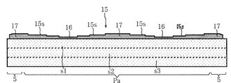
尚、メッキ用タイバー15は、図5に示すように、接続線14を介してメッキ用電極6の中央部と接続し且つ該メッキ用電極6に近接する位置16から、当該メッキ用電極6から最も離れた位置17に向かって、厚みを外側向きに階段状(段階的)15sに厚くし、隣接するメッキ用電極6,6間においても、各メッキ用電極6から最も離れた位置17に向かって階段状に厚くなるようにした形態としても良い。
また、メッキ用タイバー15は、図6に示すように、メッキ用電極6の中央部と接続し且つ該メッキ用電極6に近接する位置16から、当該メッキ用電極6から最も離れた位置17に向かって、厚みを外側向きにカーブ状(漸次的)15rに厚くし、隣接するメッキ用電極6,6間においても、各メッキ用電極6から最も離れた位置17に向かってカーブ状15rに厚くなる形態としても良い。
更に、図7に示すように、メッキ用電極6の中央部と接続し且つ該メッキ用電極6に近接する位置16から、当該メッキ用電極6から最も離れた位置17に向かって、厚みが内側向きにテーパ状(漸次的)15tに厚くし、隣接するメッキ用電極6,6間においても、各メッキ用電極6の付近から最も離れた位置17に向かってテーパ状15tに厚くなる形態のメッキ用タイバー15cとしても良い。
As shown in FIG. 5, the
Further, as shown in FIG. 6, the
Furthermore, as shown in FIG. 7, the thickness is increased from a
また、図8に示すように、メッキ用電極6の中央部と接続し且つ該メッキ用電極6に近接する位置16から、当該メッキ用電極6から最も離れた位置17に向かって、厚みが内側向きに階段状(段階的)15sに厚くし、隣接するメッキ用電極6,6間においても、各メッキ用電極6の付近から最も離れた位置17に向かって階段状に厚くなるようにしたメッキ用タイバー15cとしても良い。
加えて、図9に示すように、メッキ用電極6の中央部と接続し且つ該メッキ用電極6に近接する位置16から、当該メッキ用電極6から最も離れた位置17に向かって、厚みが内側向きにカーブ状(漸次的)15rに厚くし、隣接するメッキ用電極6,6間においても、各メッキ用電極6から最も離れた位置17に向かってカーブ状15rに厚くなる形態のメッキ用タイバー15cとしても良い。
以上の図6〜図9に示すように、メッキ用電極6に近接する位置16から、当該メッキ用電極6から最も離れた位置17に向かって、厚みが漸次的または段階的に変化するメッキ用タイバー15,15cを用いても、前記多数個取り配線基板1aと同様な効果を奏する多数個取り配線基板を構成することが可能である。
Further, as shown in FIG. 8, the thickness is inward from a
In addition, as shown in FIG. 9, the thickness increases from a
As shown in FIGS. 6 to 9 described above, the plating thickness changes gradually or stepwise from the
図10は、前記配線基板1aの応用形態の多数個取り配線基板1bを示す部分平面図、図11は、図10中のZ−Z線の矢視に沿った垂直断面図である。
多数個取り配線基板1bは、図10に示すように、前記導体枠8、接続端子11、キャビティ10などを有する複数の配線基板pを縦横に配列した前記同様の製品領域Paと、その外側に位置する前記同様の耳部5とを備えている。
該多数個取り配線基板1bが前記配線基板1aと相違するのは、図11に示すように、上下の耳辺5の表面2において、前記メッキ用タイバー15における左右のメッキ用電極6から最も離れた位置17に隣接する位置22の厚みが最も薄く、且つ各耳辺5の中央部21に向かって厚みがテーパ状(漸次的)23に外側向きに厚くなった接続(メッキ)用タイバー20が形成されていることである。
更に、図10の縦方向に沿って、上記接続用タイバー20と、製品領域Pa内の最外側に位置する配線基板pごとの導体枠20との間を接続する接続配線9j、および縦方向に隣接する配線基板pごとの導体枠8,8間を接続する接続線9fと、を更に追加して形成したことも、前記配線基板1aとの相違点である。
FIG. 10 is a partial plan view showing a multi-piece wiring board 1b as an application form of the wiring board 1a, and FIG. 11 is a vertical sectional view taken along the line ZZ in FIG.
As shown in FIG. 10, the multi-piece wiring board 1b includes the same product region Pa in which a plurality of wiring boards p having the
The multi-piece wiring board 1b is different from the wiring board 1a in that the
Furthermore, along the vertical direction of FIG. 10, the connection wiring 9j connecting between the
以上のような多数個取り配線基板1bによれば、左右一対のメッキ用タイバー15によって、前記配線基板1aと同様な効果が得られるのに加え、上下一対の接続用タイバー20、縦方向に沿った接続配線9j、および接続線9fが更に併設されることで、表面2における複数の配線基板pの導体枠8を縦方向に沿った導通経路においても、各メッキ用電極6との距離の差を、製品領域Pa内のどの位置であっても、一層低減ないし抑制して均一化することができる。従って、各メッキ用電極6に給電されたメッキ電流が、製品領域Paのどの位置における配線基板pに対しても、比較的均一に流されるため、配線基板pごとの導体枠8などの表面にNiメッキ皮膜およびAuメッキ皮膜を一層均一な厚みで被覆した多数個取り配線基板1bとすることができる。
尚、前記多数個取り配線基板1bの接続(メッキ)用タイバー20は、図12に示すように、階段状(段階的)25に厚みが変化する形態としたり、あるいはカーブ状に厚みが変化する形態としても良い。また、前記接続用タイバー20は、セラミック層s1の内部に向かってテーパ状23、階段状25、あるいはカーブ状に厚くなる形態としても良い。
According to the multi-piece wiring board 1b as described above, the pair of left and right plating tie bars 15 can provide the same effect as the wiring board 1a, and the pair of upper and lower connection tie bars 20 extends along the vertical direction. The connection wiring 9j and the
Incidentally, the
図13は、前記配線基板1a,1bとは異なる形態の多数個取り配線基板1cを示す垂直断面図、図14は、図13中のU−U線の矢視に沿った部分平面図、図15は、図14中のV−V線の矢視に沿った概略の垂直断面図である。
多数個取り配線基板1cは、図13,14に示すように、表面2および裏面3を有し且つ上下2層(複数)のセラミック層(絶縁層)s1,s2を積層してなり、厚み方向に沿った平面視で長方形(矩形)を呈する複数の配線基板pを縦横に沿って配列した製品領域Paと、上記と同じセラミック層s1,s2を積層してなり、上記製品領域Paの外周に沿って位置し且つ平面視が矩形枠状の耳部5と、該耳部5のうち、図13で左右一対の耳辺5の外側面4に一対(複数)ずつ形成したメッキ用電極6と、を含んでいる。
FIG. 13 is a vertical sectional view showing a
As shown in FIGS. 13 and 14, the
尚、前記セラミック層s1,s2も、アルミナを主成分としている。
また、図14中の破線は、個々の配線基板pの外側縁を隣接させつつ囲み、且つ製品領域Paと耳部5とを区分する仮想の切断予定面cfを示している。
図13,14に示すように、製品領域Paの表面2には、縦横に隣接する4個の配線基板pの各隅部に跨る表面導体26、および製品領域Paの最外側に沿って隣接する2個の配線基板pの各隅部に跨る表面導体26などが形成されている。即ち、追って切断予定面cfに沿って個片化された際に、得られる配線基板pごとの表面2の四隅には、4個のパッドが個別に形成される。
The ceramic layers s1 and s2 are also mainly composed of alumina.
14 indicates a virtual planned cutting plane cf that surrounds the outer edges of the individual wiring boards p while adjoining each other and separates the product region Pa and the
As shown in FIGS. 13 and 14, the
図14に示すように、前記セラミック層s1,s2間の耳部5のうち、左右一対の長辺の耳辺5には、メッキ用タイバー35が対向して形成され、上下一対の短辺の耳辺5には、接続用タイバー39が形成されている。上記メッキ用タイバー35は、図15に示すように、メッキ用電極6の中央部と直に接続し且つ該メッキ用電極6に最近接する位置36から、当該メッキ用電極6から最も離れた位置37に向かって、厚みがテーパ状(漸次的)38に厚くなるように形成されている。左右の耳辺5で隣接するメッキ用電極6,6間においても、各メッキ用電極6から最も離れた位置37に向かってテーパ状(漸次的)38に厚くなっている。尚、上記メッキ用タイバー35の厚みは、上記位置36,37間において、カーブ状(漸次的)、あるいは階段状(段階状)に変化する形態としても良い。
一方、左右の上記メッキ用タイバー35の上・下端の位置37,37間を接続する上下の各接続用タイバー39は、幅および厚みが一定であるか、あるいは前記同様に厚みのみが漸次的または段階的に変化している。
As shown in FIG. 14, among the
On the other hand, the upper and lower connecting tie bars 39 that connect the upper and
図13,図14に示すように、前記セラミック層s1,s2間には、耳部5の内周側と製品領域Paの最外側に沿って配列された複数の配線基板pの外隅、あるいは、製品領域Pa内で隣接する4個の配線基板pの各隅部に跨って形成された平面視がほぼ正方形の配線部(導体部分)30と、該配線部30,30間を水平に接続する平面視がクランク形状の連絡配線32と、外周側の配線部30と前記メッキ用タイバー35とを接続する接続配線34とが形成されている。
上記配線部30ごとの中心部には、前記セラミック層s1,s2を厚み方向に貫通するスルーホールhが位置しており、該スルーホールhの内壁面に沿ってほぼ円筒形のスルーホール導体29が形成されている。該スルーホール導体29を介して、各配線部30と前記表面導体26とが導通可能されている。図13に示すように、セラミック層s2側の裏面3には、前記表面導体26と同様な複数の裏面導体28が配線基板pごとの四隅部に形成され、上記スルーホール導体29を介して、各配線部30および表面導体26と個別に導通可能されている。
As shown in FIGS. 13 and 14, between the ceramic layers s1 and s2, outer corners of a plurality of wiring boards p arranged along the inner peripheral side of the
A through hole h penetrating the ceramic layers s1 and s2 in the thickness direction is located at the center of each
即ち、追って切断予定面cfに沿って個片化した際の配線基板pごとのセラミック層s1,s2間には、四隅付近に電気的に独立した4個の配線部が配設され、該配線部は、配線基板pごとの四隅の外側面に露出する凹溝導体を介して、表面2側のパッドや裏面3側の裏面導体(接続端子)と導通される。
尚、前記メッキ用電極6、配線部30、連絡配線32、接続配線34、表面導体26、メッキ用タイバー35、接続用タイバー39、裏面導体28、スルーホール導体29は、例えば、主にWあるいはMoからなる。
また、前記メッキ用タイバー35は、追って前記セラミック層s2となるグリーンシートの表面に、W粉末などを含む導電性ペーストを、複数回に渉って印刷した後、常法により積層・焼成することで、容易に形成されたものである。
In other words, between the ceramic layers s1 and s2 for each wiring board p when separated into pieces along the scheduled cutting plane cf, four electrically independent wiring portions are arranged near the four corners. The portion is electrically connected to the pad on the
The
Further, the
以上のような多数個取り配線基板1cによれば、セラミック層s1,s2間の耳部5において、左右一対の耳辺5に対向して形成された一対のメッキ用タイバー35の厚みは、前記一対のメッキ用電極6に近接する位置36から該メッキ用電極6から最も離れた位置37に向かって、テーパ状(漸次的)38、あるいは段階状に厚くなっている。その結果、メッキ用電極6の比較的近くに位置する製品領域Paの外周側の配線基板pと、メッキ用電極6から比較的離れた製品領域Paの中央側に位置する配線基板pとの間においも、導通経路の長短に伴う導通抵抗の差が小さくされている。従って、メッキ用電極6、メッキ用タイバー35、接続配線34、および連絡配線32を介したメッキ電流が、製品領域Paのどの位置における配線基板pに対しても、比較的均一に流されるため、配線基板pごとの表・裏面導体26,28の表面に、Niメッキ被膜やAuメッキ被膜を近似した厚みで被覆した多数個取り配線基板1cとされている。
According to the
本発明は、以上において説明した各形態に限定されるものではない。
例えば、絶縁層は、前記アルミナ以外の高温焼成セラミック、あるいは低温焼成セラミックの一種であるガラス−セラミック、更には、エポキシなどの樹脂からなるものとしても良い。このうち、ガラス−セラミックやエポキシ系樹脂を用いた場合、前記メッキ用電極6、導体枠8、メッキ用タイバー15,35、配線部30などの導体は、Cu、Ag、Cu合金、あるいはAg合金が適用される。
また、前記メッキ用電極6は、耳部5の同じ耳辺5に1個のみを設けたり、あるいは3個以上を併設した形態としても良い。
更に、前記メッキ用電極6は、耳部5における四辺の耳辺5ごとに、1個以上を同数あるいは異なる数にして形成しても良い。かかる形態では、耳部5を構成する四辺の耳辺5ごとに、前記メッキ用タイバー15,35が配設される。
また、前記メッキ用タイバー35は、複数のセラミック層(絶縁層)のうち、最上層のセラミック層の表面あるいは裏面に配設しても良く、前記メッキ用タイバー15は、複数のセラミック層(絶縁層)の間に配設しても良い。
The present invention is not limited to the embodiments described above.
For example, the insulating layer may be made of a high-temperature fired ceramic other than alumina, or a glass-ceramic which is a kind of low-temperature fired ceramic, and further a resin such as epoxy. Among these, when glass-ceramic or epoxy resin is used, the conductors such as the
Further, only one
Furthermore, one or more of the
The
更に、前記「漸次的」には、メッキ用電極に近接する位置から該メッキ用電極から離れた位置に向かって、曲線状に(カーブして)厚くなる形態も含まれる。
また、前記「段階的」には、メッキ用電極に近接する位置から該メッキ用電極から離れた位置に向かって、傾斜した複数の斜辺を介して厚みが段階的に順次厚くなる形態も含まれる。
更に、前記多数個取り配線基板1a〜1cにおいて、製品領域Paと耳部5との境界や、配線基板p,p間の境界に破線で示す仮想の切断予定面cfを配置した形態では、かかる切断予定面cfに沿ってシンター(剪断)加工することで、各配線基板pが個片化される。
加えて、前記多数個取り配線基板1a〜1cにおいて、前記切断予定面cfに替えて、表面2に開口する断面ほぼV字形の分割溝を形成したり、表面2と裏面3との双方に断面ほぼV字形の分割溝を対称に一対形成しておき、該分割溝に沿って曲げ加工することで、各配線基板pを個片化するようにしても良い。
Further, the “gradual” includes a form in which the thickness becomes curved (curved) from a position close to the plating electrode toward a position away from the plating electrode.
In addition, the “stepwise” includes a mode in which the thickness gradually increases stepwise through a plurality of inclined sides from a position close to the plating electrode to a position away from the plating electrode. .
Furthermore, in the multi-cavity wiring boards 1a to 1c, in the form in which a virtual cutting planned surface cf indicated by a broken line is arranged at the boundary between the product region Pa and the
In addition, in the multi-piece wiring boards 1a to 1c, instead of the planned cutting plane cf, a substantially V-shaped dividing groove opened on the
縦横に複数の配線基板が配列された製品領域と、メッキ用電極が外側面に形成された耳部とを併有し、上記製品領域内のどの位置における配線基板でも、その導体部分に被覆された金属メッキ被膜の厚みが均一な多数個取り配線基板を確実に提供することができる。 It has both a product area in which a plurality of wiring boards are arranged vertically and horizontally and an ear part on which an electrode for plating is formed on the outer surface, and the wiring board at any position in the product area is covered with the conductor portion. In addition, it is possible to reliably provide a multi-piece wiring board having a uniform metal plating film thickness.
1a〜1c………………多数個取り配線基板
5…………………………耳部/耳辺
6…………………………メッキ用電極
8…………………………導体枠(導体部分)
9j,34………………接続配線
15,15c,35……メッキ用タイバー
16,36………………メッキ用電極に近接する位置
17,37………………メッキ用電極から離れた位置
30………………………配線部(導体部分)
Pa………………………製品領域
p…………………………配線基板
s1〜s3………………セラミック層(絶縁層)
15t,15r,23…テーパ状/カーブ状(漸次的)
15s,25……………階段状(段階的)
1a to 1c ………………
9j, 34 ………………
Pa …………………… Product area p ………………………… Wiring board s1 to s3 ……………… Ceramic layer (insulating layer)
15t, 15r, 23 ... tapered / curved (gradual)
15s, 25 ............... Stairs (stepwise)
Claims (3)
上記同様に絶縁層を積層してなり、上記製品領域の外周に沿って位置し且つ平面視が矩形枠状である耳部と、
上記耳部の外側面に形成したメッキ用電極と、
上記耳部に形成され、上記メッキ用電極と、上記製品領域内の最外側に位置する複数の配線基板の導体部分から延びた接続配線ごと、との間を導通するメッキ用タイバーとを含み、
上記メッキ用タイバーの厚みは、上記メッキ用電極に近接する位置から該メッキ用電極から離れた位置に向かって厚くなっている、
ことを特徴とする多数個取り配線基板。 A product region in which a plurality of insulating layers are stacked, and a plurality of wiring boards that are rectangular in a plan view along the thickness direction are arranged along the length and breadth,
In the same manner as described above, an insulating layer is laminated, and an ear portion that is located along the outer periphery of the product region and has a rectangular frame shape in plan view;
A plating electrode formed on the outer surface of the ear,
A plating tie bar formed between the ears and electrically connected between the electrode for plating and the connection wires extending from the conductor portions of the plurality of wiring boards located on the outermost side in the product region;
The thickness of the plating tie bar is increased from a position close to the plating electrode toward a position away from the plating electrode.
A multi-piece wiring board characterized by that.
ことを特徴とする請求項1に記載の多数個取り配線基板。 The thickness of the plating tie bar is gradually increased from a position close to the plating electrode to a position away from the plating electrode, or is gradually increased.
The multi-piece wiring board according to claim 1, wherein:
ことを特徴とする請求項1または2に記載の多数個取り配線基板。 A plurality of the plating electrodes are formed on the outer surface of the ear portion, and the thickness of the plating tie bar connecting between two adjacent plating electrodes is the thinnest at a position close to each plating electrode. , And thickest at the position farthest from each plating electrode,
The multi-piece wiring board according to claim 1, wherein the multi-piece wiring board is provided.
Priority Applications (1)
| Application Number | Priority Date | Filing Date | Title |
|---|---|---|---|
| JP2011008385A JP5458029B2 (en) | 2011-01-19 | 2011-01-19 | Multi-wiring board |
Applications Claiming Priority (1)
| Application Number | Priority Date | Filing Date | Title |
|---|---|---|---|
| JP2011008385A JP5458029B2 (en) | 2011-01-19 | 2011-01-19 | Multi-wiring board |
Publications (2)
| Publication Number | Publication Date |
|---|---|
| JP2012151260A JP2012151260A (en) | 2012-08-09 |
| JP5458029B2 true JP5458029B2 (en) | 2014-04-02 |
Family
ID=46793251
Family Applications (1)
| Application Number | Title | Priority Date | Filing Date |
|---|---|---|---|
| JP2011008385A Active JP5458029B2 (en) | 2011-01-19 | 2011-01-19 | Multi-wiring board |
Country Status (1)
| Country | Link |
|---|---|
| JP (1) | JP5458029B2 (en) |
Families Citing this family (2)
| Publication number | Priority date | Publication date | Assignee | Title |
|---|---|---|---|---|
| JP6729046B2 (en) * | 2016-06-20 | 2020-07-22 | 大日本印刷株式会社 | Wiring board, manufacturing method thereof, and manufacturing method of semiconductor device |
| JP6816046B2 (en) * | 2018-02-06 | 2021-01-20 | アオイ電子株式会社 | Manufacturing method of semiconductor devices |
Family Cites Families (3)
| Publication number | Priority date | Publication date | Assignee | Title |
|---|---|---|---|---|
| JP2001234397A (en) * | 2000-02-24 | 2001-08-31 | Matsushita Electric Works Ltd | Electroplating jig |
| JP2004103811A (en) * | 2002-09-09 | 2004-04-02 | Kyocera Corp | Multi-cavity wiring board |
| JP4223412B2 (en) * | 2004-01-29 | 2009-02-12 | シャープ株式会社 | Plating lead evaluation program, evaluation apparatus provided with a computer-readable recording medium recording this plating lead evaluation program, and printed wiring board designed using these plating lead evaluation program or evaluation apparatus |
-
2011
- 2011-01-19 JP JP2011008385A patent/JP5458029B2/en active Active
Also Published As
| Publication number | Publication date |
|---|---|
| JP2012151260A (en) | 2012-08-09 |
Similar Documents
| Publication | Publication Date | Title |
|---|---|---|
| US10886203B2 (en) | Packaging structure with recessed outer and inner lead surfaces | |
| WO2013099854A1 (en) | Circuit board and multi-cavity circuit board | |
| US9999125B2 (en) | Method for fabricating ceramic insulator for electronic packaging | |
| JP4477202B2 (en) | Semiconductor device and manufacturing method thereof | |
| JP5957151B2 (en) | Wiring board | |
| TWI592956B (en) | Core inductor production methods | |
| JP5458029B2 (en) | Multi-wiring board | |
| JP2016192509A (en) | Chip resistor | |
| JP5706186B2 (en) | Chip resistor and manufacturing method thereof | |
| JP2006310796A (en) | Wiring board for multiple patterning | |
| JP5458028B2 (en) | Multi-wiring board | |
| JP2017076698A (en) | Wiring board and manufacturing method of the same | |
| US9349674B2 (en) | Wiring board unit, manufacturing method thereof, and manufacturing method of wiring board with lead | |
| JP6613089B2 (en) | Wiring board and manufacturing method thereof | |
| JP2009010103A (en) | Multiple patterning ceramic substrate | |
| JP6057285B2 (en) | Semiconductor device mounting substrate | |
| JP2018181972A (en) | Ceramic substrate | |
| JP7122939B2 (en) | Wiring board and manufacturing method thereof | |
| JP2019192720A (en) | Multi-piece wiring board | |
| JP4964526B2 (en) | Method for manufacturing hybrid integrated circuit board | |
| JP2006269603A (en) | Wiring board and multi-patterned wiring board | |
| JP2018078152A (en) | Chip resistor | |
| JP2017017081A (en) | Multi-piece wiring board | |
| JP2009194000A (en) | Multiple wiring board | |
| JP6763607B2 (en) | Lead frame and its manufacturing method |
Legal Events
| Date | Code | Title | Description |
|---|---|---|---|
| A621 | Written request for application examination |
Free format text: JAPANESE INTERMEDIATE CODE: A621 Effective date: 20130415 |
|
| A977 | Report on retrieval |
Free format text: JAPANESE INTERMEDIATE CODE: A971007 Effective date: 20131203 |
|
| TRDD | Decision of grant or rejection written | ||
| A01 | Written decision to grant a patent or to grant a registration (utility model) |
Free format text: JAPANESE INTERMEDIATE CODE: A01 Effective date: 20131217 |
|
| A61 | First payment of annual fees (during grant procedure) |
Free format text: JAPANESE INTERMEDIATE CODE: A61 Effective date: 20140110 |
|
| R150 | Certificate of patent or registration of utility model |
Ref document number: 5458029 Country of ref document: JP Free format text: JAPANESE INTERMEDIATE CODE: R150 Free format text: JAPANESE INTERMEDIATE CODE: R150 |
|
| R250 | Receipt of annual fees |
Free format text: JAPANESE INTERMEDIATE CODE: R250 |
|
| R250 | Receipt of annual fees |
Free format text: JAPANESE INTERMEDIATE CODE: R250 |
|
| R250 | Receipt of annual fees |
Free format text: JAPANESE INTERMEDIATE CODE: R250 |
|
| R250 | Receipt of annual fees |
Free format text: JAPANESE INTERMEDIATE CODE: R250 |
|
| R250 | Receipt of annual fees |
Free format text: JAPANESE INTERMEDIATE CODE: R250 |
|
| R250 | Receipt of annual fees |
Free format text: JAPANESE INTERMEDIATE CODE: R250 |
|
| S531 | Written request for registration of change of domicile |
Free format text: JAPANESE INTERMEDIATE CODE: R313531 |
|
| R350 | Written notification of registration of transfer |
Free format text: JAPANESE INTERMEDIATE CODE: R350 |
|
| R250 | Receipt of annual fees |
Free format text: JAPANESE INTERMEDIATE CODE: R250 |
|
| R250 | Receipt of annual fees |
Free format text: JAPANESE INTERMEDIATE CODE: R250 |
|
| R250 | Receipt of annual fees |
Free format text: JAPANESE INTERMEDIATE CODE: R250 |