JP5448272B2 - LIGHT EMITTING DEVICE, DISPLAY MODULE AND ELECTRONIC DEVICE - Google Patents
LIGHT EMITTING DEVICE, DISPLAY MODULE AND ELECTRONIC DEVICE Download PDFInfo
- Publication number
- JP5448272B2 JP5448272B2 JP2011258501A JP2011258501A JP5448272B2 JP 5448272 B2 JP5448272 B2 JP 5448272B2 JP 2011258501 A JP2011258501 A JP 2011258501A JP 2011258501 A JP2011258501 A JP 2011258501A JP 5448272 B2 JP5448272 B2 JP 5448272B2
- Authority
- JP
- Japan
- Prior art keywords
- circuit
- mode
- display
- signal
- transistor
- Prior art date
- Legal status (The legal status is an assumption and is not a legal conclusion. Google has not performed a legal analysis and makes no representation as to the accuracy of the status listed.)
- Expired - Fee Related
Links
Images


Landscapes
- Control Of Indicators Other Than Cathode Ray Tubes (AREA)
- Control Of El Displays (AREA)
Description
本発明は表示装置、特にアクティブマトリクス型表示装置に関する。 The present invention relates to a display device, and more particularly to an active matrix display device.
近年、画素を発光ダイオード(LED)などの発光素子で形成した、いわゆる自発光型
の表示装置が注目を浴びている。このような自発光型の表示装置に用いられる発光素子と
しては、有機発光ダイオード(OLED(Organic Light Emittin
g Diode)、有機EL素子、エレクトロルミネッセンス(Electro Lum
inescence:EL)素子などとも言う)が注目を集めており、ELディスプレイ
(例えば、有機ELディスプレイなど)に用いられるようになってきている。OLEDな
どの発光素子は自発光型であるため、液晶ディスプレイに比べて画素の視認性が高く、バ
ックライトが不要で応答速度が速い等の利点がある。また発光素子の輝度は、そこを流れ
る電流値によって制御される。
In recent years, so-called self-luminous display devices in which pixels are formed by light-emitting elements such as light-emitting diodes (LEDs) have attracted attention. As a light-emitting element used in such a self-luminous display device, an organic light-emitting diode (OLED (Organic Light Emittin) is used.
g Diode), organic EL element, electroluminescence (Electro Lum)
insence (EL) element) has attracted attention and has been used for EL displays (for example, organic EL displays). Since light-emitting elements such as OLEDs are self-luminous, there are advantages such as higher pixel visibility than a liquid crystal display, no need for a backlight, and high response speed. The luminance of the light emitting element is controlled by the value of current flowing therethrough.
このような表示装置の発光階調を制御する駆動方式として、デジタル階調方式とアナログ
階調方式とがある。デジタル階調方式はデジタル制御で発光素子をオンオフさせ、階調を
表現している。一方、アナログ階調方式には、発光素子の発光強度をアナログ制御する方
式と発光素子の発光時間をアナログ制御する方式がある。
There are a digital gradation method and an analog gradation method as driving methods for controlling the light emission gradation of such a display device. In the digital gradation method, gradation is expressed by turning on and off the light emitting element by digital control. On the other hand, the analog gray scale method includes a method in which the light emission intensity of the light emitting element is controlled in analog and a method in which the light emission time of the light emitting element is controlled in analog.
デジタル階調方式の場合、発光・非発光の2状態しかないため、このままでは、2階調
しか表現できない。そこで、別の手法を組み合わせて、多階調化を図ることが行われてい
る。多階調化のための手法としては、時間階調法を用いられることが多い(特許文献1〜
特許文献2参照)。
In the digital gradation method, since there are only two states of light emission and non-light emission, only two gradations can be expressed as it is. In view of this, multi-gradation is being achieved by combining different methods. A time gradation method is often used as a method for multi-gradation (
Patent Document 2).
デジタル制御で画素の表示状態を制御して、時間階調を組み合わせて階調を表現するデ
ィスプレイとしては、デジタル階調方式を用いた有機ELディスプレイの他にも、いくつ
か存在する。例としては、プラズマディスプレイなどがある。
In addition to the organic EL display using the digital gradation method, there are several displays that display gradation by combining the time gradation by controlling the display state of the pixel by digital control. An example is a plasma display.
時間階調法とは、発光している期間の長さや、発光した回数を制御して、階調を表現す
る方法である。つまり、1フレーム期間を複数のサブフレーム期間に分割し、各サブフレ
ームに、発光回数や発光時間などの重み付けを行い、重み付けの総量(発光回数の総和や
、発光時間の総和)を階調ごとに差を付けることによって、階調を表現している。
The time gradation method is a method of expressing gradation by controlling the length of a light emitting period and the number of times of light emission. In other words, one frame period is divided into a plurality of subframe periods, and each subframe is weighted such as the number of times of light emission and the time of light emission, and the total amount of weighting (total number of times of light emission and total time of light emission) is assigned for each gradation. The gradation is expressed by adding a difference to.
このように、アナログ階調方式とデジタル階調方式とがあるが、双方とも、長所と短所が
あり、両方の長所を兼ね備えたような方式がなかった。そのため、どちらかの方式に限定
せざるを得なかった。
As described above, there are an analog gradation method and a digital gradation method, but both have advantages and disadvantages, and there is no method that has both advantages and disadvantages. For this reason, it was inevitably limited to either method.
本発明はこのような問題点に鑑み、アナログ階調方式とデジタル階調方式の両方の長所
を持つような表示装置を提供することを目的とする。
In view of such problems, the present invention has an object to provide a display device having advantages of both an analog gradation method and a digital gradation method.
本発明は、複数の表示モードを持ち、切り替えて表示できるような手段を有する表示装
置を提供する。つまり、ソースドライバが、アナログ階調方式とデジタル階調方式とを切
り替えて動作させるような手段を有している。このような手段を用いて、アナログ階調方
式とデジタル階調方式の両方の長所もつように出来ることにより、上記目的を達成するも
のである。
The present invention provides a display device having a plurality of display modes and means capable of switching and displaying. That is, the source driver has means for switching between the analog gradation method and the digital gradation method. By using such means, the above object can be achieved by having the advantages of both the analog gradation method and the digital gradation method.
本発明の表示装置は、複数の画素がマトリクス状に配置された表示装置であって、前記表
示装置は、ソースドライバとゲートドライバとを有し、前記ソースドライバは、デジタル
値とアナログ値のいずれか一つの信号を、前記画素に供給する回路を有していることを特
徴とする表示装置。
The display device of the present invention is a display device in which a plurality of pixels are arranged in a matrix, and the display device includes a source driver and a gate driver, and the source driver is either a digital value or an analog value. A display device comprising a circuit for supplying one signal to the pixel.
本発明の表示装置は、複数の画素がマトリクス状に配置された表示装置であって、前記
表示装置は、ソースドライバとゲートドライバとを有し、前記ソースドライバは、アナロ
グデジタル切替回路を有していることを特徴とする表示装置。
The display device of the present invention is a display device in which a plurality of pixels are arranged in a matrix, and the display device has a source driver and a gate driver, and the source driver has an analog / digital switching circuit. A display device.
本発明の表示装置は、複数の画素がマトリクス状に配置された表示装置であって、前記
表示装置は、少なくとも2つの表示モードを有し、第1の表示モードにおいて、前記画素
にアナログ信号が供給され、第2の表示モードにおいて、前記画素にデジタル信号が供給
されることを特徴としている。
The display device of the present invention is a display device in which a plurality of pixels are arranged in a matrix, and the display device has at least two display modes. In the first display mode, an analog signal is output to the pixels. In the second display mode, a digital signal is supplied to the pixel.
本発明の表示装置は、複数の画素がマトリクス状に配置された表示装置であって、前記
表示装置は、少なくとも2つの表示モードを有し、前記画素は、発光素子を有し第1の表
示モードにおいて、前記画素にアナログ信号が供給され、第2の表示モードにおいて、前
記画素にデジタル信号が供給され、前記発光素子に供給させる電圧が、前記第1の表示モ
ードと前記第2の表示モードとで異なることを特徴としている。
The display device of the present invention is a display device in which a plurality of pixels are arranged in a matrix. The display device has at least two display modes, and the pixels have light emitting elements and have a first display. In the mode, an analog signal is supplied to the pixel, and in the second display mode, a digital signal is supplied to the pixel, and the voltage supplied to the light emitting element is the first display mode and the second display mode. It is characterized by being different.
本発明の表示装置は、複数の画素がマトリクス状に配置された表示装置であって、前記
表示装置は、少なくとも2つの表示モードを有し、前記画素は、発光素子とトランジスタ
とを有し、前記発光素子の第1の電極と、前記トランジスタのソース電極またはドレイン
電極の一方とが接続され第1の表示モードにおいて、前記画素にアナログ信号が供給され
、第2の表示モードにおいて、前記画素にデジタル信号が供給され、前記発光素子の第2
の電極と、前記トランジスタのソース電極またはドレイン電極の他方との間の電圧は、前
記第1の表示モードと前記第2の表示モードとで異なることを特徴としている。
The display device of the present invention is a display device in which a plurality of pixels are arranged in a matrix, the display device has at least two display modes, and the pixel includes a light emitting element and a transistor, The first electrode of the light emitting element is connected to one of the source electrode or the drain electrode of the transistor, and an analog signal is supplied to the pixel in the first display mode. In the second display mode, the pixel is supplied to the pixel. A digital signal is supplied, and a second of the light emitting elements
The voltage between the first electrode and the other of the source electrode and the drain electrode of the transistor is different between the first display mode and the second display mode.
本発明においては、一画素とは、明るさを制御できる要素一つ分を示すものとする。よ
って、一例としては、一画素とは、一つの色要素を示すものとし、その色要素一つで明る
さを表現する。従って、そのときは、R(赤)G(緑)B(青)の色要素からなるカラー
表示装置の場合には、画像の最小単位は、Rの画素とGの画素とBの画素との三画素から
構成されるものとする。なお、色要素は、三色に限定されず、それ以上でもよく、例えば
、RGBW(Wは白)がある。
In the present invention, one pixel represents one element whose brightness can be controlled. Therefore, as an example, one pixel represents one color element, and brightness is expressed by one color element. Therefore, at that time, in the case of a color display device composed of R (red), G (green), and B (blue) color elements, the minimum unit of an image is an R pixel, G pixel, and B pixel. It is assumed to be composed of three pixels. The color elements are not limited to three colors and may be more than that, for example, RGBW (W is white).
なお、本明細書において、画素がマトリクスに配置されているとは、縦縞と横縞を組み
合わせたいわゆる格子状に配置されている場合はもちろんのこと、三色の色要素(例えば
RGB)でフルカラー表示を行う場合に、1つの画像の最小要素を表す三つの色要素の画
素がいわゆるデルタ配置されている場合も含むものとする。また、ベイヤー配置されてい
る場合も含む。また、色要素毎に色の発光領域が異なっていてもよい。
Note that in this specification, the pixels are arranged in a matrix, not only in the case of a so-called grid pattern in which vertical stripes and horizontal stripes are combined, but also in full-color display with three color elements (for example, RGB). When performing the above, the case where pixels of three color elements representing the minimum element of one image are arranged in a so-called delta arrangement is also included. Moreover, the case where a Bayer arrangement is also included. Further, the color light emitting region may be different for each color element.
本発明において、適用可能なトランジスタの種類に限定はなく、非晶質シリコンや多結
晶シリコンに代表される非単結晶半導体膜を用いた薄膜トランジスタ(TFT)、半導体
基板やSOI基板を用いて形成されるMOS型トランジスタ、接合型トランジスタ、バイ
ポーラトランジスタ、有機半導体やカーボンナノチューブを用いたトランジスタ、その他
のトランジスタを適用することができる。なお、非単結晶半導体膜には水素またはハロゲ
ンが含まれていてもよい。また、トランジスタが配置されている基板の種類に限定はなく
、単結晶基板、SOI基板、ガラス基板、プラスチック基板、紙基板、セロファン基板、
石材基板などに配置することが出来る。また、ある基板でトランジスタを形成し、その後
、別の基板にトランジスタを移動させて、別の基板上に配置するようにしてもよい。
In the present invention, there are no limitations on the types of transistors that can be used, and the transistor is formed using a thin film transistor (TFT) using a non-single-crystal semiconductor film typified by amorphous silicon or polycrystalline silicon, a semiconductor substrate, or an SOI substrate. A MOS transistor, a junction transistor, a bipolar transistor, a transistor using an organic semiconductor or a carbon nanotube, and other transistors can be used. Note that the non-single-crystal semiconductor film may contain hydrogen or halogen. There is no limitation on the type of the substrate on which the transistor is disposed, and a single crystal substrate, an SOI substrate, a glass substrate, a plastic substrate, a paper substrate, a cellophane substrate,
It can be placed on a stone substrate. Alternatively, a transistor may be formed using a certain substrate, and then the transistor may be moved to another substrate and placed on another substrate.
なお、上述したように、本発明におけるトランジスタは、どのようなタイプのトランジ
スタでもよいし、どのような基板上に形成されていてもよい。したがって、回路の全てガ
ラス基板上に形成されていてもよいし、プラスチック基板や単結晶基板に形成されていて
もよいし、SOI基板上に形成されていてもよいし、どのような基板上に形成されていて
もよい。回路の全てが形成されていることにより、部品数を減らしてコストを低減したり
、回路部品との接続数を減らすことにより、信頼性を向上させたりすることができる。あ
るいは、回路の一部をある基板に形成し、回路の別の一部を別の基板に形成してもよい。
つまり、回路の全てが同じ基板上に形成されていなくてもよい。例えば、回路の一部は、
ガラス基板上にトランジスタを用いて形成し、回路の別の一部は、単結晶基板等の上に形
成したICチップをCOG(Chip On Glass)により接続してガラス基板上
に配置してもよい。あるいは、そのICチップをTAB(Tape Auto Bond
ing)やプリント基板を用いてガラス基板と接続してもよい。このように、回路の一部
が同じ基板に形成されていることにより、部品数を減らしてコストを低減したり、回路部
品との接続点数を減らすことにより信頼性を向上させたりすることができる。また、駆動
電圧が高い部分や駆動周波数が高い部分は、消費電力が大きくなるため、そのような部分
は同じ基板に形成しないようにすれば、消費電力の向上を防ぐことができる。
As described above, the transistor in the present invention may be any type of transistor and may be formed on any substrate. Therefore, the entire circuit may be formed on a glass substrate, may be formed on a plastic substrate or a single crystal substrate, may be formed on an SOI substrate, or on any substrate. It may be formed. Since all the circuits are formed, the number of parts can be reduced to reduce the cost, and the number of connections with circuit parts can be reduced to improve the reliability. Alternatively, a part of the circuit may be formed on a certain substrate and another part of the circuit may be formed on another substrate.
That is, all of the circuits may not be formed on the same substrate. For example, part of the circuit
Another part of the circuit may be formed on a glass substrate by connecting an IC chip formed on a single crystal substrate or the like with a COG (Chip On Glass). . Alternatively, the IC chip is a TAB (Tape Auto Bond).
ing) or a printed circuit board. As described above, since a part of the circuit is formed on the same substrate, the number of components can be reduced to reduce the cost, and the reliability can be improved by reducing the number of connection points with the circuit components. . In addition, since power consumption is high in a portion where the drive voltage is high or a portion where the drive frequency is high, improvement in power consumption can be prevented if such a portion is not formed on the same substrate.
なお、明細書に示すスイッチは、様々な形態のものを用いることができ、一例として、
電気的スイッチや機械的なスイッチなどがある。つまり、電流の流れを制御できるもので
あればよく、特に限定されない。例えば、トランジスタでもよいし、ダイオード(PNダ
イオード、PINダイオード、ショットキーダイオード、ダイオード接続のトランジスタ
など)でもよいし、それらを組み合わせた論理回路でもよい。スイッチとしてトランジス
タを用いる場合、そのトランジスタは単なるスイッチとして動作するため、トランジスタ
の極性(導電型)は特に限定されない。ただし、オフ電流が少ない方の極性のトランジス
タを用いることが望ましい。オフ電流が少ないトランジスタとしては、LDD領域を設け
ているものやマルチゲート構造にしているものなどがある。また、スイッチとして動作さ
せるトランジスタのソース電極の電位が、低電位側電源(Vss、GND、0Vなど)に
近い状態で動作する場合はNチャネル型を、反対にソース電極の電位が、高電位側電源(
Vddなど)に近い状態で動作する場合はPチャネル型を用いることが望ましい。なぜな
ら、ゲートソース間電圧の絶対値を大きくすることができるため、スイッチとして動作し
やすいからである。なお、Nチャネル型とPチャネル型の両方を用いて、CMOS型のス
イッチにしてもよい。CMOS型のスイッチにすると、様々な入力電圧に対し出力電圧を
制御しやすいため、適切な動作を行うことができる。
Note that the switch shown in the specification can be used in various forms, and as an example,
There are electrical switches and mechanical switches. That is, it is not particularly limited as long as the current flow can be controlled. For example, a transistor, a diode (a PN diode, a PIN diode, a Schottky diode, a diode-connected transistor, or the like), or a logic circuit that is a combination thereof may be used. In the case of using a transistor as a switch, the transistor operates as a mere switch, and thus the polarity (conductivity type) of the transistor is not particularly limited. However, it is desirable to use a transistor having a polarity with a smaller off-state current. As a transistor with low off-state current, there are a transistor provided with an LDD region and a transistor having a multi-gate structure. In addition, when the transistor operates as a switch with the source electrode potential close to the low potential side power supply (Vss, GND, 0 V, etc.), the N channel type is used. Power supply(
When operating in a state close to Vdd, etc., it is desirable to use a P-channel type. This is because the absolute value of the gate-source voltage can be increased, so that it can easily operate as a switch. Note that both N-channel and P-channel switches may be used as CMOS switches. When a CMOS type switch is used, the output voltage can be easily controlled with respect to various input voltages, so that an appropriate operation can be performed.
なお、本発明において接続されているとは、電気的に接続されていることと同義である
。したがって、本発明が開示する構成において、所定の接続関係に加え、その間に電気的
な接続を可能とする他の素子(例えば、スイッチやトランジスタや容量素子やインダクタ
や抵抗素子やダイオードなど)が配置されていてもよい。もちろん、間に他の素子を介さ
ずに配置されていてもよく、電気的に接続されているとは直接的に接続されている場合を
含むものとする。
In the present invention, being connected is synonymous with being electrically connected. Therefore, in the configuration disclosed by the present invention, in addition to a predetermined connection relationship, other elements (for example, a switch, a transistor, a capacitor, an inductor, a resistor, a diode, etc.) that can be electrically connected are arranged. May be. Of course, it may be arranged without interposing other elements in between, and being electrically connected includes the case of being directly connected.
なお、本発明において、接続されているとは、電気的に接続されていることと同義であ
る。したがって、本発明が開示する構成において、所定の接続関係に加え、その間に電気
的な接続を可能とする他の素子(例えば、別の素子やスイッチなど)が配置されていても
よい。
In the present invention, being connected is synonymous with being electrically connected. Therefore, in the configuration disclosed by the present invention, in addition to a predetermined connection relationship, another element (for example, another element or a switch) that enables electrical connection may be disposed therebetween.
なお、本発明において、ある物の上に形成されている、あるいは〜上に形成されている
、というように、〜の上に、あるいは、〜上に、という記載については、ある物の上に直
接接していることに限定されない。直接接してはいない場合、つまり間に別のものが挟ま
っている場合も含むものとする。従って例えば、層Aの上に(もしくは層A上に)層Bが
形成されているという場合は、層Aの上に直接接して層Bが形成されている場合と、層A
の上に別の層(例えば層Cや層Dなど)が形成されており、その上に層Bが形成されてい
る場合とを含むものとする。また、〜の上方に、という記載についても同様であり、ある
物の上に直接接していることに限定されず、間に別のものが挟まっている場合も含むもの
とする。従って、例えば層Aの上方に層Bが形成されている、という場合は、層Aの上に
直接接して層Bが形成されている場合と、層Aの上に別の層(例えば層Cや層Dなど)が
形成されおり、その上に層Bが形成されている場合とを含むものとする。なお、〜の下、
もしくは〜の下方にの場合についても、同様に直接接している場合と、接していない場合
とを含むこととする。
In addition, in this invention, it is formed on a certain thing, or is formed on the top. It is not limited to being in direct contact. This includes cases where they are not in direct contact, that is, when another object is sandwiched between them. Therefore, for example, when the layer B is formed on the layer A (or on the layer A), the case where the layer B is formed in direct contact with the layer A and the case where the layer A is formed
And the case where another layer (for example, the layer C or the layer D) is formed on the layer B and the layer B is formed thereon. The same applies to the description of “above”, and it is not limited to being in direct contact with a certain object, and includes a case where another object is sandwiched therebetween. Therefore, for example, when the layer B is formed above the layer A, when the layer B is formed directly on the layer A, another layer (for example, the layer C) is formed on the layer A. And the layer D) are formed, and the layer B is formed thereon. In addition, under
Or the case below-also includes the case where it touches directly, and the case where it is not touching similarly.
本発明では、アナログ階調方式とデジタル階調方式とを切り替えて表示することがが可
能となる。したがって、コントラストなどの表示品位が向上し、消費電力が低減すること
が出来るようになる。
In the present invention, the display can be switched between the analog gradation method and the digital gradation method. Therefore, display quality such as contrast is improved, and power consumption can be reduced.
以下、本発明の実施の形態について図面を参照しながら説明する。但し、本発明は多くの
異なる態様で実施することが可能であり、本発明の趣旨及びその範囲から逸脱することな
くその形態及び詳細を様々に変更し得ることは当業者であれば容易に理解される。従って
本実施の形態の記載内容に限定して解釈されるものではない。
Hereinafter, embodiments of the present invention will be described with reference to the drawings. However, the present invention can be implemented in many different modes, and those skilled in the art can easily understand that the modes and details can be variously changed without departing from the spirit and scope of the present invention. Is done. Therefore, the present invention is not construed as being limited to the description of this embodiment mode.
(実施の形態1)
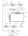
図1に、全体の構成図を示す。画素配列101を駆動するために、ソースドライバ102
、ゲートドライバ103が配置されている。なお、ソースドライバ102、ゲートドライ
バ103は、各々複数個配置されていてもよい。
(Embodiment 1)
FIG. 1 shows an overall configuration diagram. In order to drive the
The
なお、ソースドライバやその一部は、画素配列101と同一基板上に存在せず、例えば
、外付けのICチップを用いて構成されることもある。
Note that the source driver and a part of the source driver do not exist on the same substrate as the
なお、すでに述べたように、本発明におけるトランジスタは、どのようなタイプのトラ
ンジスタでもよいし、どのような基板上に形成されていてもよい。したがって、図1で示
したような回路が、全てガラス基板上に形成されていてもよいし、プラスチック基板に形
成されていてもよいし、単結晶基板に形成されていてもよいし、SOI基板上に形成され
ていてもよいし、どのような基板上に形成されていてもよい。あるいは、図1などにおけ
る回路の一部が、ある基板に形成されており、図1などにおける回路の別の一部が、別の
基板に形成されていてもよい。つまり、図1などにおける回路の全てが同じ基板上に形成
されていなくてもよい。例えば、図1などにおいて、画素配列101とゲートドライバ1
03とは、ガラス基板上にTFTを用いて形成し、ソースドライバ102(もしくはその
一部)は、単結晶基板上に形成し、そのICチップをCOG(Chip On Glas
s)で接続してガラス基板上に配置してもよい。あるいは、そのICチップをTAB(T
ape Auto Bonding)やプリント基板を用いてガラス基板と接続してもよ
い。
Note that as described above, the transistor in the present invention may be any type of transistor, and may be formed on any substrate. Accordingly, the circuit as shown in FIG. 1 may be entirely formed on a glass substrate, may be formed on a plastic substrate, may be formed on a single crystal substrate, or may be an SOI substrate. It may be formed on any substrate, and may be formed on any substrate. Alternatively, a part of the circuit in FIG. 1 or the like may be formed on a certain substrate, and another part of the circuit in FIG. 1 or the like may be formed on another substrate. That is, all the circuits in FIG. 1 and the like may not be formed on the same substrate. For example, in FIG. 1 and the like, the
03 is formed using a TFT on a glass substrate, the source driver 102 (or part thereof) is formed on a single crystal substrate, and the IC chip is formed by COG (Chip On Glass).
It may be connected on s) and placed on the glass substrate. Alternatively, the IC chip is TAB (T
Ape Auto Bonding) or a printed circuit board may be used to connect to the glass substrate.
ソースドライバ102は、大きく3つの部分に分けることが出来る。
The
まず、シフトレジスタ110は、順次選択していくような信号(いわゆるサンプリングパ
ルス)を出力する回路である。よって、同様な機能を果たす回路であれば、シフトレジス
タに限定されない。例えば、デコーダ回路でもよい。
First, the
シフトレジスタが出力するサンプリングパルスは、アナログデジタル切り替え回路104
に入力される。アナログデジタル切り替え回路104には、ビデオ信号線108を通って
ビデオ信号106が入力される。そして、入力されたビデオ信号106を、デジタルデー
タ処理回路105に入力するのか、画素配列に入力するのかを、表示モード制御信号10
7を用いて制御する機能を有している。表示モード制御信号107は、表示モード制御信
号線109を通って、アナログデジタル切り替え回路104に入力される。例えば、表示
モード制御信号107がH信号や有意レベルの信号の時には、ビデオ信号106は、画素
配列101に入力される。逆に、表示モード制御信号107がL信号や非有意レベルの信
号の時には、ビデオ信号106は、デジタルデータ処理回路105に入力される。
The sampling pulse output from the shift register is the analog /
Is input. A video signal 106 is input to the analog /
7 has a function to control. The display mode control signal 107 is input to the analog /
デジタルデータ処理回路105は、通常のデジタルドライバと同様な機能を有している。
すなわち、ビデオ信号106を保持し、保持したビデオ信号106を画素配列101に出
力する機能を有している。
The digital
That is, it has a function of holding the video signal 106 and outputting the held video signal 106 to the
したがって、表示モード制御信号107により、画素配列101には、ビデオ信号106
をそのまま入力することと、デジタルデータ処理回路105に一旦保持したあとで、画素
配列101に入力する場合とを切り替えることが出来る。
Therefore, the video signal 106 is sent to the
Can be switched between being input to the
よって、画素配列101にビデオ信号106をそのまま入力するときには、画素配列10
1に入力されるデオ信号はアナログ値とすることが可能となる。その場合、画素はアナロ
グ的に制御されることが可能になる。したがって、アナログ階調方式を用いることが出来
る。
Therefore, when the video signal 106 is input to the
The video signal input to 1 can be an analog value. In that case, the pixel can be controlled in an analog fashion. Therefore, an analog gradation method can be used.
一方、ビデオ信号106をデジタルデータ処理回路105に一旦保持する場合は、アナロ
グ値でデータを保持することが困難であるため、ビデオ信号106はデジタル値の場合と
なる。よって、画素は、デジタル的に制御されることになる。したがって、デジタル階調
方式を用いることとなる。
On the other hand, when the video signal 106 is temporarily held in the digital
ただし、ビデオ信号106を一旦保持する場合であっても、容量素子などを用いれば、ア
ナログ値で信号を保存することも可能である。
However, even when the video signal 106 is held once, the signal can be stored as an analog value by using a capacitor or the like.
そこで、表示モードとして、アナログ階調方式を用いる場合をアナログモード、デジタル
階調方式を用いる場合をデジタルモードと呼ぶことにする。
Therefore, as a display mode, a case where an analog gradation method is used is called an analog mode, and a case where a digital gradation method is used is called a digital mode.
以上のことから、表示モード制御信号107により、アナログ階調方式とデジタル階調方
式とを切り替えることが可能となる。
From the above, it is possible to switch between the analog gradation method and the digital gradation method by the display mode control signal 107.
次に、図1の構成を具体化した場合を図2に示す。なお、図2では、簡単のため、2列分
の場合に関して記載したが、これに限定されない。任意に列数を増やすことが出来る。
Next, FIG. 2 shows a case where the configuration of FIG. 1 is embodied. In FIG. 2, the case of two columns is described for simplicity, but the present invention is not limited to this. The number of columns can be increased arbitrarily.
アナログデジタル切り替え回路104において、サンプリングスイッチ201、202が
、シフトレジスタ110から順次出力されるサンプリングパルスにより制御される。そし
て、モード選択用スイッチ203、204は、表示モード制御信号107により制御され
る。モード選択用スイッチ203、204は、排他的にオンオフする。つまり、モード選
択用スイッチ203、204のいずれか一方がオンのときは、他方がオフになる。このモ
ード選択用スイッチにより、ビデオ信号106を一旦デジタルデータ処理回路105に入
力するのか、画素配列101に入力するのかを制御する。図2の場合、モード選択用スイ
ッチ203がオンのとき、ビデオ信号106は、サンプリングスイッチ201とモード選
択用スイッチ203を通って、画素配列101に伝達される。同様に、モード選択用スイ
ッチ205がオンのとき、ビデオ信号106は、サンプリングスイッチ202とモード選
択用スイッチ205を通って、画素配列101に伝達される。一方、モード選択用スイッ
チ204がオンのとき、ビデオ信号106は、サンプリングスイッチ201とモード選択
用スイッチ204を通って、デジタルデータ処理回路105に伝達される。同様に、モー
ド選択用スイッチ206がオンのとき、ビデオ信号106は、サンプリングスイッチ20
2とモード選択用スイッチ206を通って、デジタルデータ処理回路105に伝達される
。
In the analog /
2 and the
デジタルデータ処理回路105では、ラッチ1回路207やラッチ2回路208において
、ビデオ信号の保存と出力が行われる。ラッチ1回路207には、シフトレジスタ110
から順次出力されるサンプリングパルスにしたがって、ビデオ信号106が入力され、保
存される。そして、1行分のビデオ信号106を保存した後、ラッチ信号211により、
ラッチ1回路に保存されていたビデオ信号106がラッチ2回路208に転送される。こ
のような動作を行うことにより、線順次駆動が可能となる。ラッチ2回路208からは、
出力制御スイッチ209、210を介して、画素配列101にビデオ信号が出力される。
出力制御スイッチ209、210は、表示モード制御信号107に応じて制御される。つ
まり、ラッチ2回路208の出力を画素配列101に入力したい場合、例えば、デジタル
モードの場合は、出力制御スイッチ209、210はオンする。逆に、ラッチ2回路20
8の出力を画素配列101に入力したくない場合、例えば、アナログモードの場合は、出
力制御スイッチ209、210はオフする。その結果、ビデオ信号106は、モード選択
用スイッチ203、205を通って、画素配列101に入力される。
In the digital
The video signal 106 is input and stored in accordance with sampling pulses sequentially output from. After storing the video signal 106 for one row, the
The video signal 106 stored in the
A video signal is output to the
The output control switches 209 and 210 are controlled according to the display mode control signal 107. That is, when it is desired to input the output of the latch 2
When it is not desired to input the output of 8 to the
ここで、図3に、ラッチ1回路207とラッチ2回路208の例を示す。クロックドイン
バータやインバータを用いて、構成されている。なお、図3の構成に限定されない。
Here, FIG. 3 shows an example of the
なお、図3のようなラッチ1回路207とラッチ2回路208を有するデジタルデータ処
理回路105を用いる場合、図2におけるサンプリングスイッチ201、202などは、
省略することが出来る。なぜなら、図3のようなデジタルデータ処理回路105を用いる
場合、サンプリングスイッチ201、202が無くても、デジタルデータ処理回路105
にデータが入ってしまうことを防ぐことが出来るからである。
When the digital
It can be omitted. This is because when the digital
This is because data can be prevented from entering.
また、画素配列101には、画素220がマトリクス状に配置されている。1画素分の画
素220の例を図4に示す。ゲート信号線401を用いて、選択用トランジスタ404を
制御する。選択用トランジスタ404がオンすると、ソース信号線402から、保持容量
405にビデオ信号が入力される。すると、ビデオ信号に応じて、駆動トランジスタ40
6がオンオフし、電源線403から発光素子407を通って、対向電極408へ電流が流
れる。
In the
6 is turned on and off, and a current flows from the
図4における電源線403は、図2における電源線221へと接続される。また、図4に
おける対向電極408は、図2における配線222へと接続される。配線222は、全て
の画素の対向電極に接続されている場合が多い。ただし、これに限定されない。
The
なお、画素構成は、図4に限定されない。例えば、駆動トランジスタのバラツキを補正す
るような構成でもよい。
Note that the pixel configuration is not limited to FIG. For example, a configuration that corrects variations in driving transistors may be used.
バラツキを補正する画素構成としては、大きく分けて、しきい値電圧のバラツキを補正す
るタイプと、ビデオ信号として電流を入力するタイプとがある。
The pixel configuration for correcting variation is roughly divided into a type for correcting variation in threshold voltage and a type for inputting current as a video signal.
図32に、しきい値電圧のバラツキを補正する画素構成を示す。スイッチ3107をゲー
ト信号線3115を用いて制御することにより、駆動トランジスタ3101のしきい値電
圧を容量素子3104に保存する。また、ゲート信号線3114により制御されるスイッ
チ3103は、駆動トランジスタ3101のゲート電位を初期化する機能を果たす。そし
て、ソース信号線3111からスイッチ3102を通ってビデオ信号を入力する。なお、
スイッチ3102はゲート信号線3113により制御される。図4における保持容量40
5は容量素子3105に、駆動トランジスタ406は駆動トランジスタ3101に、電源
線403は電源線3116に相当する。
FIG. 32 shows a pixel configuration for correcting variations in threshold voltage. By controlling the
The
5 corresponds to the
図32では、駆動トランジスタ3101のゲート電位を初期化するための配線3112が
必要であったが、それを削除したものを図33に示す。駆動トランジスタ3101のゲー
トは、スイッチ3203を介して、駆動トランジスタ3101のドレインに接続されてい
る。
In FIG. 32, the
なお、しきい値電圧のバラツキを補正する画素構成には、さまざまなものがあり、図32
,図33の構成に限定されない。このように、しきい値電圧のバラツキを補正する画素構
成を用いると、発光素子に流れる電流のバラツキを低減することができる。特に、アナロ
グモードにおいて、輝度を均一にできる。よって、より好適である。
There are various pixel configurations for correcting variations in threshold voltage, and FIG.
The configuration is not limited to that shown in FIG. As described above, when a pixel configuration that corrects variation in threshold voltage is used, variation in current flowing in the light-emitting element can be reduced. In particular, the luminance can be made uniform in the analog mode. Therefore, it is more preferable.
次に、ビデオ信号として電流を入力するタイプの画素構成を図34に示す。ソース信号線
3330にビデオ信号に応じた電流が供給される。すると、選択用スイッチ3302を介
して駆動トランジスタ3301のドレインに、スイッチ3304を介して駆動トランジス
タ3301のゲートにその電流が流れ、それに応じて、ゲート・ソース間電圧が発生する
。そのゲート・ソース間電圧は、容量素子3305に保存され、その後、スイッチ330
6を介して発光素子に電流が供給される。なお、選択用スイッチ3302、スイッチ33
04及びスイッチ3306のそれぞれは、ゲート信号線3333、ゲート信号線3334
、ゲート信号線3335により制御されている。なお、3336は電源線を示す。なお、
図34では、信号電流を供給されるトランジスタと、発光素子に電流を供給するトランジ
スタとは同一であるが、異なっていても良い。その場合を図35に示す。信号電流を供給
されるトランジスタ3401と、発光素子に電流を供給するトランジスタ3421とは、
別である。なお、図35中の3411はソース線、3413と3414はゲート信号線、
3402は選択用スイッチ、3404はスイッチ、3405は容量素子、3416は電源
線を示す。
Next, FIG. 34 shows a pixel configuration in which a current is input as a video signal. A current corresponding to the video signal is supplied to the
A current is supplied to the light emitting element via 6. The
04 and the
The
In FIG. 34, the transistor supplied with the signal current and the transistor supplying the current to the light emitting element are the same, but may be different. This case is shown in FIG. A
It is another. In FIG. 35, 3411 is a source line, 3413 and 3414 are gate signal lines,
なお、電流を入力してバラツキを補正する画素構成には、さまざまなものがあり、図34
、図35の構成に限定されない。このように、電流を入力してバラツキを補正する画素構
成を用いると、発光素子に流れる電流のバラツキを低減することができる。特に、アナロ
グモードにおいて、輝度を均一にできる。よって、より好適である。
Note that there are various pixel configurations for correcting variations by inputting current, and FIG.
The configuration is not limited to that shown in FIG. As described above, when a pixel configuration in which variation is corrected by inputting a current, variation in current flowing in the light-emitting element can be reduced. In particular, the luminance can be made uniform in the analog mode. Therefore, it is more preferable.
なお、画素に配置するのは、特定の発光素子に限定されない。画素に配置する表示素子の
例としては、EL素子(エレクトロルミネッセンス(Electro Luminesc
ence:EL);有機発光ダイオード((Organic Light Emitti
ng Diode:OLED)、有機EL素子などとも言う)の他、無機EL素子又は有
機物及び無機物を含むEL素子)や電子放出素子、液晶素子、電子インクなど電気磁気的
作用によりコントラストが変化する表示媒体を適用することができる。また、電子放出素
子にカーボンナノチューブを利用することも可能ある。なお、電子放出素子を用いた表示
装置としてはフィールドエミッションディスプレイ(FED)で用いる素子、FEDの一
種であるSED(Surface−conduction Electron−emit
ter Display)などが挙げられる。その他、液晶ディスプレイ(LCD)、プ
ラズマディスプレイ(PDP)、電子ペーパーディスプレイ、デジタルマイクロミラーデ
バイス(DMD)、圧電セラミックディスプレイなどに用いる、どのような表示素子でも
よい。
Note that the pixel is not limited to a specific light-emitting element. As an example of a display element arranged in a pixel, an EL element (Electro Luminescence)
ence: EL); organic light emitting diode ((Organic Light Emitter)
ng Diode (OLED), also referred to as an organic EL element), inorganic EL elements or EL elements including organic and inorganic substances), electron-emitting elements, liquid crystal elements, electronic inks, and the like whose display medium changes contrast due to an electromagnetic action. Can be applied. In addition, carbon nanotubes can be used for the electron-emitting device. Note that a display device using an electron-emitting device is an element used in a field emission display (FED), a SED (Surface-Conduction Electron-emit) which is a kind of FED.
ter Display). In addition, any display element used for a liquid crystal display (LCD), a plasma display (PDP), an electronic paper display, a digital micromirror device (DMD), a piezoelectric ceramic display, or the like may be used.
なお、図4における保持容量405は、駆動トランジスタ406のゲート電位を保持す
る役目をしている。よって、駆動トランジスタ406のゲートと電源線403の間に接続
されているが、これに限定されない。駆動トランジスタ406のゲート電位を保持できる
ように配置されていればよい。また、駆動トランジスタ406のゲート容量などを用いて
、駆動トランジスタ406のゲート電位を保持できる場合は、保持容量405を省いても
良い。
Note that the
なお、図1などに示すスイッチ、例えば、サンプリングスイッチ201やモード選択用
スイッチ203や出力制御スイッチ209等は、電気的スイッチでも機械的なスイッチで
も何でも良い。電流の流れを制御できるものなら、何でも良い。トランジスタでもよいし
、ダイオードでもよいし、それらを組み合わせた論理回路でもよい。よって、スイッチと
してトランジスタを用いる場合、そのトランジスタは、単なるスイッチとして動作するた
め、トランジスタの極性(導電型)は特に限定されない。ただし、オフ電流が少ない方が
望ましい場合、オフ電流が少ない方の極性のトランジスタを用いることが望ましい。オフ
電流が少ないトランジスタとしては、LDD領域を設けているものや、マルチゲート構造
にしたもの等がある。また、スイッチとして動作させるトランジスタのソース端子の電位
が、低電位側電源(Vss、Vgnd、0Vなど)に近い状態で動作する場合はnチャネ
ル型を、反対に、ソース端子の電位が、高電位側電源(Vddなど)に近い状態で動作す
る場合はpチャネル型を用いることが望ましい。なぜなら、ゲート・ソース間電圧の絶対
値を大きくできるため、スイッチとして、動作しやすいからである。なお、nチャネル型
とpチャネル型の両方を用いて、CMOS型のスイッチにしてもよい。
Note that the switches shown in FIG. 1 and the like, for example, the
スイッチの例を図5に示す。図5(A)は、模式的に記載したスイッチである。図5(B
)は、AND回路を用いたスイッチである。制御線502を使って、入力501の信号を
出力503に伝えるかどうかを制御する。図5(B)の場合は、出力503は、入力信号
にかかわらず、L信号なる、というような制御は可能である。しかし、出力503がフロ
ーティング状態になることはない。したがって、出力503が、デジタル回路の入力に接
続されている場合などに、図5(B)のスイッチを用いることが好適である。デジタル回
路の場合、入力をフローティング状態にしても、出力はフローティング状態にならない。
入力をフローティング状態にすると、出力が不安定になり、望ましくない。よって、デジ
タル回路の入力に接続されている場合などは、図5(B)のスイッチを用いることが好適
である。
An example of the switch is shown in FIG. FIG. 5A is a switch schematically described. FIG.
) Is a switch using an AND circuit. A
If the input is in a floating state, the output becomes unstable, which is undesirable. Therefore, when connected to the input of a digital circuit, the switch in FIG. 5B is preferably used.
なお、図5(B)は、AND回路を用いて構成したが、これに限定されない。OR回路や
NAND回路やNOR回路を用いても、同様の機能を果たすことが出来る。
Note that although FIG. 5B is configured using an AND circuit, the present invention is not limited to this. Even if an OR circuit, a NAND circuit, or a NOR circuit is used, the same function can be achieved.
一方、入力をフローティング状態にしたい場合は、図5(C)や図5(D)のスイッチを
用いればよい。図5(C)は、トランスミッションゲートもしくはアナログスイッチなど
と呼ばれている回路である。図5(C)は、入力511の電位を、ほぼそのまま出力51
3に伝達する。よって、アナログ信号の伝達に好適である。図5(D)は、クロックドイ
ンバータなどと呼ばれている回路である。図5(D)は、入力521の信号を反転させて
出力523に伝達する。よって、デジタル信号の伝達に好適である。なお、制御線512
、522により、それぞれ入力511、521の信号を出力513、523に伝えるかど
うかを制御する。
On the other hand, when the input is desired to be in a floating state, the switches in FIGS. 5C and 5D may be used. FIG. 5C illustrates a circuit called a transmission gate or an analog switch. In FIG. 5C, the potential of the input 511 is almost the same as the output 51.
3 is transmitted. Therefore, it is suitable for transmitting analog signals. FIG. 5D illustrates a circuit called a clocked inverter or the like. In FIG. 5D, the signal of the input 521 is inverted and transmitted to the output 523. Therefore, it is suitable for transmission of digital signals. The
522 controls whether the signals of the inputs 511 and 521 are transmitted to the outputs 513 and 523, respectively.
以上のことから、サンプリングスイッチ201などや、アナログ信号を伝達するモード選
択用スイッチ203などは、図5(C)のスイッチを用いることが好適である。デジタル
信号を伝達するモード選択用スイッチ204は、デジタル回路であるラッチ1回路207
の入力に接続されているので、図5(B)のスイッチを用いることが好適である。出力制
御スイッチ209などは、出力をフローティング状態にする必要があるので、図5(C)
や図5(D)が好適である。ただし、出力制御スイッチ209への入力はデジタル信号な
ので、図5(D)の方がより好適である。
From the above, it is preferable to use the switches in FIG. 5C for the
Therefore, it is preferable to use the switch shown in FIG. 5B. Since the
FIG. 5D is preferable. However, since the input to the
(実施の形態2)
本実施の形態では、アナログモードにおける画素の駆動方法について述べる。
(Embodiment 2)
In this embodiment, a method for driving a pixel in an analog mode is described.
図6に、駆動トランジスタと発光素子とに加わる電圧と電流の関係を示す。図6(A)は
、駆動トランジスタ601と発光素子602の回路を示す。配線603と配線604の間
に、駆動トランジスタ601と発光素子602とが直列に接続されている。配線603の
方が配線604よりも電位が高いため、駆動トランジスタ601から発光素子602の方
へ電流が流れる。
FIG. 6 shows the relationship between the voltage and current applied to the drive transistor and the light emitting element. FIG. 6A shows a circuit of the driving
図4における駆動トランジスタ406が、図6(A)における駆動トランジスタ601に
相当し、図4における発光素子407が、図6(A)における発光素子602に相当する
。
A
図6(B)に、駆動トランジスタ601のゲート・ソース間電圧(の絶対値)と、駆動ト
ランジスタ601と発光素子602とに流れる電流の関係を示す。ゲート・ソース間電圧
(の絶対値)を大きくしていくと、それに応じて、電流値も大きくなっていく。これは、
駆動トランジスタ601が飽和領域で動作しているためである。飽和領域では、トランジ
スタのゲート・ソース電圧の2乗に比例して電流値が増えていく。さらにゲート・ソース
間電圧(の絶対値)を大きくしていくと、発光素子602に加わる電圧が大きくなるため
、ドレイン・ソース電圧が小さくなり、駆動トランジスタ601が線形領域で動作するよ
うになる。すると、ドレイン・ソース電圧が小さくなるにしたがって、電流値の上昇率も
小さくなっていく。そして、ある電流値以上の電流は流れなくなる。
FIG. 6B shows the relationship between the gate-source voltage (the absolute value thereof) of the driving
This is because the driving
アナログモードでは、アナログ階調方式を用いて階調を表現する。したがって、駆動トラ
ンジスタ601のゲート・ソース間電圧(の絶対値)をアナログ的に変化させることによ
って、駆動トランジスタ601と発光素子602とに流れる電流もアナログ的に変化する
ような状態で動作させることが望ましい。そのため、駆動トランジスタ601のゲート・
ソース間電圧(の絶対値)は、しきい値電圧から、駆動トランジスタ601が飽和領域と
して動作するゲート・ソース間電圧にかけて変化させれば良い。なお、変化させる上限は
、飽和領域にとどまらず線形領域にかけて変化させても良い。即ち、駆動トランジスタ6
01のゲート・ソース間電圧(の絶対値)は、ゲート・ソース間電圧(の絶対値)に対し
電流値IELが変化する領域であれば良い。また、変化させる下限値は、駆動トランジス
タ601がオフとなるゲート・ソース間電圧(の絶対値)であれば良い。
In the analog mode, gradation is expressed using an analog gradation method. Therefore, by changing the gate-source voltage (absolute value) of the driving
The source voltage (absolute value) may be changed from the threshold voltage to the gate-source voltage at which the driving
The gate-source voltage (absolute value) of 01 may be a region where the current value I EL changes with respect to the gate-source voltage (absolute value). Further, the lower limit value to be changed may be a gate-source voltage (an absolute value thereof) at which the driving
例えば、電圧範囲620のように、電流が殆どながれないようなところから、飽和領域内
で動作するような状態で、駆動トランジスタ601のゲート・ソース間電圧(の絶対値)
を制御してもよい。電流が殆どながれないような状態とは、駆動トランジスタ601のゲ
ート・ソース間電圧が、駆動トランジスタ601のしきい値電圧とほぼ等しい場合に相当
する。
For example, the voltage between the gate and the source of the driving transistor 601 (the absolute value thereof) in a state where the current hardly flows as in the
May be controlled. The state where almost no current flows corresponds to the case where the gate-source voltage of the driving
あるいは、電圧範囲621のように、駆動トランジスタ601のゲート・ソース間電圧が
、駆動トランジスタ601のしきい値電圧よりも確実に低い状態から、ゲート・ソース間
電圧(の絶対値)を大きくしていって制御し、飽和領域内で動作するような状態で、駆動
トランジスタ601のゲート・ソース間電圧(の絶対値)を制御してもよい。このように
、黒状態のときの、駆動トランジスタ601のゲート・ソース間電圧を、駆動トランジス
タ601のしきい値電圧よりも確実に低い電圧にすることにより、確実に黒状態にするこ
とができる。例えば、駆動トランジスタ601の電流特性がばらついたとき、しきい値電
圧もばらつく。よって、ある画素では黒状態になっていても、別の画素では、僅かに発光
してしまうこともある。その結果、コントラストの低下を招いてしまう。そこで、それを
防止するため、621のような電圧範囲で動作させることは、好適である。
Alternatively, the gate-source voltage (absolute value) is increased from a state where the gate-source voltage of the driving
なお、電圧範囲620や電圧範囲621では、駆動トランジスタ601のゲート・ソース
間電圧(の絶対値)を大きくしても、飽和領域で動作するとしたが、これに限定されない
。電圧範囲622や電圧範囲623のように、飽和領域だけでなく、線形領域も使って動
作させてもよい。駆動トランジスタ601のゲート・ソース間電圧(の絶対値)をアナロ
グ的に変化させることによって、駆動トランジスタ601と発光素子602とに流れる電
流もアナログ的に変化するような範囲であれば、線形領域でも動作させてもよい。
Note that although the
なお、駆動トランジスタ601を飽和領域で動作させた場合には、たとえ発光素子60
2が劣化しても発光素子に一定の電流量を供給することが可能である。また、線形領域の
場合には、トランジスタの特性ばらつきの影響を受けずに駆動させることができる。
Note that when the driving
Even if 2 deteriorates, a constant amount of current can be supplied to the light emitting element. In the case of a linear region, the transistor can be driven without being affected by variations in transistor characteristics.
次に、発光素子602からの光の色によって、最適化させた場合について述べる。発光素
子602は、色によって、輝度が異なったり、必要な電流値が異なったりしている。そこ
で、色バランスを合わせる必要がある。そのためには、駆動トランジスタ601のゲート
・ソース間電圧(の絶対値)を色ごとに異なるようにすることが望ましい。あるいは、駆
動トランジスタ601の電流供給能力(たとえば、トランジスタのチャネル幅など)を色
ごとに異なるようにすることが望ましい。あるいは、発光素子602の発光面積を色ごと
に異なるようにすることが望ましい。あるいは、これらの幾つかを組み合わせることが望
ましい。これにより、色バランスを合わせることが可能となる。
Next, a case where optimization is performed according to the color of light from the
なお、配線603の電位を色ごとに変えることも可能である。ただし、駆動トランジスタ
601をオフにするときの電圧も色ごとに変わってしまうという欠点がある。よって、配
線603の電位は、全ての色で同じにしてもよい。
Note that the potential of the
なお、駆動トランジスタ601は、Pチャネル型の場合について述べたが、これに限定さ
れない。Nチャネル型にして、電流が流れる向きを逆にすることは、同業者であれば、容
易に実現できる。また、Pチャネル型の場合、Nチャネル型の場合、各々について、電流
が流れる向きを逆にすることも、同業者であれば、容易に実現できる。その場合は、ゲー
ト・ソース間電圧の大きさは、発光素子602の電圧電流特性の影響を受けることとなる
。
Note that although the driving
なお、本実施の形態は、実施の形態1の画素について詳細に述べたものである。よって、
本実施の形態で述べた内容は、実施の形態1で述べた内容と自由に組み合わせることが出
来る。
Note that this embodiment mode describes the pixel of
The contents described in this embodiment can be freely combined with the contents described in
(実施の形態3)
本実施の形態では、デジタルモードにおける画素の駆動方法について述べる。
(Embodiment 3)
In this embodiment, a method for driving a pixel in a digital mode is described.
図6(B)の、駆動トランジスタ601のゲート・ソース間電圧(の絶対値)と、駆動ト
ランジスタ601と発光素子602とに流れる電流の関係を参照する。デジタルモードで
は、オンとオフや、HとLのように、2値で制御する。つまり、発光素子602に電流が
流れるか、流れないかを制御する。したがって、まず、電流が流れない場合について考え
る。その場合は、駆動トランジスタ601のゲート・ソース間電圧(の絶対値)は、電圧
624、電圧625、電圧626に示すように、0V以上で、かつ、電流が流れない場合
、つまり、駆動トランジスタ601のしきい値電圧以下であればよい。
Reference is made to the relationship between the gate-source voltage (the absolute value thereof) of the driving
次に、電流が流れる場合について考える。その場合は、駆動トランジスタ601のゲート
・ソース間電圧(の絶対値)は、電圧627、628、629に示すように、飽和領域内
か、線形領域か、さらに電圧を大きくして、電流値が増えなくなっている領域などで動作
させればよい。なお、図中では電圧627は、線形領域と飽和領域の境界に位置している
が、前述のように飽和領域内であれば良い。このように、駆動トランジスタ601より発
光素子602に電流が供給できる電圧であれば特に限定されない。
Next, consider the case where current flows. In that case, the gate-source voltage (the absolute value thereof) of the driving
例えば、飽和領域で動作させる場合は、発光素子602の電圧電流特性が劣化しても、そ
こを流れる電流値が変化しない、という利点がある。そのため、焼き付きの影響を受けに
くい。ただし、駆動トランジスタ601の電流特性がばらつくと、そこを流れる電流もば
らついてしまう。そのため、表示ムラを生じてしまう場合がある。
For example, when operating in the saturation region, there is an advantage that even if the voltage-current characteristics of the
それに対して、線形領域で動作させると、駆動トランジスタ601の電流特性がばらつい
ても、そこを流れる電流値は影響を受けにくい。そのため、表示ムラが生じにくい。また
、駆動トランジスタ601のゲート・ソース間電圧(の絶対値)が大きくなりすぎないこ
とと、配線603と配線604との間の電圧を大きくしておく必要がないため、消費電力
も小さくできる。
On the other hand, when operating in the linear region, even if the current characteristics of the driving
さらに、駆動トランジスタ601のゲート・ソース間電圧(の絶対値)を大きくすると、
駆動トランジスタ601の電流特性がばらついても、そこを流れる電流値は影響をほとん
ど受けなくなる。ただし、発光素子602の電圧電流特性が劣化すると、そこを流れる電
流値が変化してしまう場合がある。そのため、焼き付きの影響を受けやすくなる。
Further, when the gate-source voltage (absolute value) of the driving
Even if the current characteristics of the
このように、駆動トランジスタ601を飽和領域で動作させると、発光素子602の特性
が変化しても、電流値が変化しない。よって、その場合、駆動トランジスタ601は、電
流源として動作していると見なせる。したがって、このような駆動を定電流駆動と呼ぶこ
とにする。
As described above, when the driving
また、駆動トランジスタ601を線形領域で動作させると、駆動トランジスタ601の電
流特性がばらついても、電流値が変化しない。よって、その場合、駆動トランジスタ60
1は、スイッチとして動作していると見なせる。よって、発光素子602には、配線60
3の電圧がそのまま加わっているように見なせる。したがって、このような駆動を定電圧
駆動と呼ぶことにする。
Further, when the driving
1 can be regarded as operating as a switch. Therefore, the
It can be considered that the voltage of 3 is applied as it is. Therefore, such driving is called constant voltage driving.
デジタルモードにおいては、定電圧駆動を用いても良いし、定電流駆動を用いても良い
。ただし、定電圧駆動を用いると、トランジスタのバラツキの影響を受けず、消費電力も
小さくなるため、好適である。
In the digital mode, constant voltage driving or constant current driving may be used. However, it is preferable to use constant voltage driving because it is not affected by transistor variation and power consumption is reduced.
次に、発光素子602の発光色によって、最適化させた場合について述べる。定電流駆動
の場合は、アナログモードと同様である。
Next, a case where the
定電圧駆動の場合は、駆動トランジスタ601のゲート・ソース間電圧(の絶対値)や、
駆動トランジスタ601の電流供給能力(たとえば、トランジスタ幅など)を色ごとに異
なるようにしても、そこを流れる電流値は、あまり変わらない。なぜなら、スイッチとし
て動作しているからである。
In the case of constant voltage driving, the gate-source voltage (absolute value) of the driving
Even if the current supply capability (for example, transistor width) of the
そのため、発光素子602の発光面積を色ごとに異なるようにすることが望ましい。ある
いは、配線603の電位を色ごとに変えることも可能である。あるいは、これらを組み合
わせることが望ましい。これにより、色バランスを合わせることが可能となる。
Therefore, it is desirable that the light emitting area of the
なお、本実施の形態は、実施の形態1の画素について詳細に述べたものである。よって、
本実施の形態で述べた内容は、実施の形態1や実施の形態2で述べた内容と自由に組み合
わせることが出来る。
Note that this embodiment mode describes the pixel of
The contents described in this embodiment can be freely combined with the contents described in
(実施の形態4)
デジタルモードの場合、このままでは、発光と非発光の2値しか表現できない。そこで、
他の方法を組み合わせて、多階調化を図ってもよい。そこで、多階調化を図った場合の画
素の駆動方法について述べる。
(Embodiment 4)
In the digital mode, only binary values of light emission and non-light emission can be expressed as it is. there,
Other methods may be combined to increase the number of gradations. Therefore, a pixel driving method in the case of increasing the number of gradations will be described.
多階調化を図る方法として、時間階調方式と面積階調方式とがある。時間階調方式は、あ
る期間の中で発光している時間の長さを変えることにより、階調を表現する方法である。
一方、面積階調方式は、発光している面積の大きさを変えることにより、階調を表現する
方法である。
There are a time gray scale method and an area gray scale method as a method for increasing the number of gray scales. The time gray scale method is a method of expressing a gray scale by changing the length of time during which light is emitted in a certain period.
On the other hand, the area gradation method is a method of expressing gradation by changing the size of a light emitting area.
なお、時間階調方式と面積階調方式とを組み合わせても良い。 Note that the time gray scale method and the area gray scale method may be combined.
ここでは、時間階調方式について、詳細に述べる。デジタル時間階調方式では、1フレー
ム期間を複数のサブフレーム期間に分割する。そして、各サブフレーム期間における点灯
期間の長さを変えることにより、階調を表現する。
Here, the time gray scale method will be described in detail. In the digital time gray scale method, one frame period is divided into a plurality of subframe periods. Then, gradation is expressed by changing the length of the lighting period in each subframe period.
まず、画素に信号を書き込む期間と点灯する期間とが分離されている場合のタイミングチ
ャートを図7に示す。まず、信号書き込み期間において、1画面分の信号を全画素に入力
する。この間は、画素は点灯しない。信号書き込み期間が終了したのち、点灯期間が始ま
り、画素が点灯する。次に、次のサブフレームが始まり、信号書き込み期間において、1
画面分の信号を全画素に入力する。この間は、画素は点灯しない。信号書き込み期間が終
了したのち、点灯期間が始まり、画素が点灯する。
First, FIG. 7 shows a timing chart in the case where a period for writing a signal to a pixel and a lighting period are separated. First, in a signal writing period, a signal for one screen is input to all pixels. During this time, the pixels are not lit. After the signal writing period ends, the lighting period starts and the pixels are lit. Next, the next subframe starts, and in the signal writing period, 1
The screen signal is input to all pixels. During this time, the pixels are not lit. After the signal writing period ends, the lighting period starts and the pixels are lit.
同様のことを繰り返すことにより、階調を表現することが可能となる。このとき、各サ
ブフレーム期間における点灯期間の長さを、1:2:4:8:・・・というように、2の
べき乗にすることにより、様々な階調を表現することが出来る。
By repeating the same thing, it becomes possible to express gradation. At this time, various gradations can be expressed by setting the length of the lighting period in each subframe period to a power of 2, such as 1: 2: 4: 8:.
その場合の画素構成は、図4の構成を用いればよい。 In that case, the pixel configuration in FIG. 4 may be used.
なお、信号書き込み期間においては、電源線403と対向電極408の電位を制御するこ
とにより、発光素子407には電圧が加わらないようにしておく。例えば、対向電極40
8の電位を高くして、発光素子407に電圧が加わらないようにしたり、対向電極408
に電荷を供給せず、フローティング状態にしてもよい。その結果、信号書き込み期間にお
いて、発光素子407が点灯することを避けることが出来る。
Note that in the signal writing period, the potential of the
8 to increase the potential of the light-emitting
A charge may not be supplied to the battery, and it may be in a floating state. As a result, the
次に、画素に信号を書き込む期間と点灯する期間とが分離されていない場合のタイミング
チャートを図8に示す。各行において、信号書き込み動作を行うと、すぐに点灯期間が開
始する。
Next, FIG. 8 shows a timing chart in the case where the period for writing a signal to the pixel and the lighting period are not separated. When a signal writing operation is performed in each row, the lighting period starts immediately.
ある行において、信号を書き込み、所定の点灯期間が終了したのち、次のサブフレームに
おける信号の書き込み動作を開始する。これを繰り返すことにより、点灯期間の長さを各
々制御することができる。
In a certain row, a signal is written, and after a predetermined lighting period ends, a signal writing operation in the next subframe is started. By repeating this, the length of the lighting period can be controlled.
このようにすることにより、信号の書き込み動作が遅くても、1フレーム内にたくさんの
サブフレームを配置することが可能となる。また、1フレーム期間における点灯期間の割
合(いわゆるデューティー比)を大きくできるので、消費電力を低減したり、発光素子の
劣化を抑制したり、疑似輪郭を抑制することが可能となる。
This makes it possible to arrange many subframes in one frame even if the signal writing operation is slow. Further, since the ratio of the lighting period in one frame period (so-called duty ratio) can be increased, power consumption can be reduced, deterioration of the light emitting element can be suppressed, and pseudo contour can be suppressed.
その場合の画素構成は、図4の構成を用いればよい。その場合、図8において、時刻t0
の場合、同時に3行分の画素に信号を入力する必要がある。通常は、同時に複数行の画素
に信号を入力することは出来ない。そこで、図9に示すように、1ゲート選択期間を複数
(図9では3つ)に分割する。そして、分割された選択期間内で、各々のゲート信号線4
01を選択し、その時に対応する信号をソース信号線402に入力する。例えば、ある1
ゲート選択期間において、G1(t0)ではi行目を選択し、G2(t0)ではj行目を
選択し、G3(t0)ではk行目を選択する。すると、1ゲート選択期間において、あた
かも同時に3行分を選択したかのように動作させることが可能となる。
In that case, the pixel configuration in FIG. 4 may be used. In that case, in FIG.
In this case, it is necessary to input signals to the pixels for three rows at the same time. Normally, signals cannot be input to a plurality of rows of pixels at the same time. Therefore, as shown in FIG. 9, one gate selection period is divided into a plurality (three in FIG. 9). Then, each of the gate signal lines 4 within the divided selection period.
01 is selected, and the corresponding signal at that time is input to the
In the gate selection period, the i-th row is selected in G1 (t0), the j-th row is selected in G2 (t0), and the k-th row is selected in G3 (t0). Then, it is possible to operate as if three rows are simultaneously selected in one gate selection period.
なお、図8、図9では、同時に3行分の画素に信号を入力する場合について示したが、
これに限定されない。さらに多くの行やさらに少ない行に信号を入力してもよい。
8 and 9 show the case where signals are simultaneously input to pixels for three rows.
It is not limited to this. Signals may be input to more or fewer rows.
なお、このような駆動方法の詳細については、例えば、特開2001−324958号公
報等に記載されており、その内容を本願と組み合わせて適用することが出来る。
Details of such a driving method are described in, for example, Japanese Patent Application Laid-Open No. 2001-324958, and the contents thereof can be applied in combination with the present application.
次に、画素の信号を消去する動作を行う場合のタイミングチャートを図10に示す。各行
において、信号書き込み動作を行い、次の信号書き込み動作が来る前に、画素の信号を消
去する。このようにすることにより、点灯期間の長さを容易に制御できるようになる。
Next, FIG. 10 shows a timing chart in the case of performing an operation of erasing the pixel signal. In each row, a signal writing operation is performed, and the pixel signal is erased before the next signal writing operation is performed. In this way, the length of the lighting period can be easily controlled.
ある行において、信号を書き込み、所定の点灯期間が終了したのち、次のサブフレームに
おける信号の書き込み動作を開始する。もし、点灯期間が短い場合は、信号消去動作を行
い、非点灯状態にする。このようなを繰り返すことにより、点灯期間の長さを制御するこ
とが出来る。
In a certain row, a signal is written, and after a predetermined lighting period ends, a signal writing operation in the next subframe is started. If the lighting period is short, a signal erasing operation is performed to turn off the light. By repeating this, the length of the lighting period can be controlled.
このようにすることにより、信号の書き込み動作が遅くても、1フレーム内にたくさんの
サブフレームを配置することが可能となる。また、消去動作を行う場合は、消去用のデー
タをビデオ信号と同様に取得する必要がないため、ソースドライバの駆動周波数も低減出
来る。
This makes it possible to arrange many subframes in one frame even if the signal writing operation is slow. Further, when performing an erasing operation, it is not necessary to acquire erasing data in the same manner as a video signal, so that the driving frequency of the source driver can be reduced.
その場合の画素構成を図11に示す。消去トランジスタ1104が、駆動トランジスタ4
06のゲートと電源線403の間に接続されている。
FIG. 11 shows a pixel configuration in that case. The erasing
06 is connected between the
ゲート信号線401を用いて、選択用トランジスタ404を制御する。選択用トランジス
タ404がオンすると、ソース信号線402から、保持容量405にビデオ信号が入力さ
れる。すると、ビデオ信号に応じて、駆動トランジスタ406がオンオフし、電源線40
3から発光素子407を通って、対向電極408へ電流が流れる。
The
A current flows from 3 through the
信号を消去したい場合は、第2ゲート線1101を選択して、消去トランジスタ1104
をオン状態にして、駆動トランジスタ406がオフ状態になるようにする。すると、電源
線403から発光素子407を通って、対向電極408へ電流が流れないようになる。そ
の結果、非点灯期間を作ることができ、点灯期間の長さを自由に制御できるようになる。
When the signal is to be erased, the
Is turned on so that the driving
図11では、消去トランジスタ1104を用いていたが、別の方法を用いることも出来る
。なぜなら、強制的に非点灯期間をつくればよいので、発光素子407に電流が供給され
ないようにすればよいからである。よって、電源線403から発光素子407を通って、
対向電極408へ電流が流れる経路のどこかに、スイッチを配置して、そのスイッチのオ
ンオフを制御して、非点灯期間を作ればよい。あるいは、駆動トランジスタ406のゲー
ト・ソース間電圧を制御して、駆動トランジスタが強制的にオフになるようにすればよい
。
Although the erase
A non-lighting period may be created by arranging a switch somewhere in the path of current flow to the
駆動トランジスタを強制的にオフにする場合の画素構成の例を図12に示す。消去ダイ
オード1204が、駆動トランジスタ406のゲートと第2ゲート線1201との間に接
続されている。
FIG. 12 shows an example of a pixel configuration when the driving transistor is forcibly turned off. An erasing
信号を消去したい場合は、第2ゲート線1201を選択(ここでは、高い電位にする)し
て、消去ダイオード1204がオンして、第2ゲート線1201から駆動トランジスタ4
06のゲートへ電流が流れるようにする。その結果、駆動トランジスタ406がオフ状態
になる。すると、電源線403から、発光素子407を通って、対向電極408には、電
流が流れないようになる。その結果、非点灯期間を作ることができ、点灯期間の長さを自
由に制御できるようになる。
When the signal is to be erased, the
The current flows to the gate of 06. As a result, the driving
信号を保持しておきたい場合は、第2ゲート線1201を非選択(ここでは、低い電位に
する)しておく。すると、消去ダイオード1204がオフするので、駆動トランジスタ4
06のゲート電位は保持される。
When it is desired to hold a signal, the
The gate potential of 06 is maintained.
なお、消去ダイオード1204は、整流性がある素子であれば、なんでもよい。PN型
ダイオードでもよいし、PIN型ダイオードでもよいし、ショットキー型ダイオードでも
よいし、ツェナー型ダイオードでもよい。
The erasing
また、トランジスタを用いて、ダイオード接続(ゲートとドレインを接続)して、用い
ても良い。その場合の回路図を図13に示す。消去ダイオード1204として、ダイオー
ド接続したトランジスタ1304を用いている。ここでは、Nチャネル型を用いているが
、これに限定されない。Pチャネル型を用いても良い。
Alternatively, a transistor may be used by diode connection (gate and drain connected). A circuit diagram in that case is shown in FIG. As the erasing
さらに、図4の回路を用いて、図10のような駆動法を実現することも可能である。その
場合のタイミングチャートは、図9と同様にすればよい。図9では、1ゲート選択期間を
3つに分割しているが、1ゲート選択期間をここでは、2つに分割する。そして、分割さ
れた選択期間内で、各々のゲート線を選択し、その時に対応する信号(ビデオ信号と消去
するための信号)をソース信号線402に入力する。例えば、ある1ゲート選択期間にお
いて、前半はi行目を選択し、後半はj行目を選択する。そして、i行目が選択されてい
るときは、それようのビデオ信号を入力する。一方、j行目が選択されているときは、駆
動トランジスタがオフするような信号を入力する。すると、1ゲート選択期間において、
あたかも同時に2行分を選択したかのように動作させることが可能となる。
Furthermore, the driving method as shown in FIG. 10 can be realized by using the circuit of FIG. The timing chart in that case may be the same as that in FIG. In FIG. 9, one gate selection period is divided into three, but here, one gate selection period is divided into two. Then, each gate line is selected within the divided selection period, and a signal (a video signal and a signal for erasing) corresponding to the gate line is input to the
It is possible to operate as if two lines were selected at the same time.
なお、このような駆動方法の詳細については、例えば、特開2001−324958号公
報等に記載されており、その内容を本願と組み合わせて適用することが出来る。
Details of such a driving method are described in, for example, Japanese Patent Application Laid-Open No. 2001-324958, and the contents thereof can be applied in combination with the present application.
なお、本実施の形態において示したタイミングチャートや画素構成や駆動方法は一例であ
り、これに限定されない。様々なタイミングチャートや画素構成や駆動方法に適用するこ
とが可能である。
Note that the timing chart, the pixel configuration, and the driving method shown in this embodiment mode are examples, and the present invention is not limited to this. The present invention can be applied to various timing charts, pixel configurations, and driving methods.
なお、本実施の形態は、実施の形態1〜実施の形態3の画素について詳細に述べたもので
ある。よって、本実施の形態で述べた内容は、実施の形態1〜実施の形態3で述べた内容
と自由に組み合わせることが出来る。
In this embodiment, the pixels of
(実施の形態5)
デジタルモードの場合、このままでは、発光と非発光の2値しか表現できない。ただし、
2値のみで表示を行ってもよい。2値のみで表示を行うことによって、消費電力を大幅に
低減することが可能となる。このような表示モードを2値モードと呼ぶことにする。
(Embodiment 5)
In the digital mode, only binary values of light emission and non-light emission can be expressed as it is. However,
You may display only with two values. By displaying with only two values, it is possible to significantly reduce power consumption. Such a display mode is called a binary mode.
ここでは、2値モードで表示を行うについて、詳細に述べる。画素構成については、実施
の形態4で述べた様々な構成を用いればよい。
Here, the display in the binary mode will be described in detail. As the pixel configuration, various configurations described in Embodiment Mode 4 may be used.
まず、実施の形態4で述べた各々の駆動方法と同程度の速度で、行をスキャンしながら信
号を書き込んでいく場合のタイミングチャートを図14(A)に示す。この場合、同程度
の周波数でソースドライバやゲートドライバを動作させることになるので、それらのドラ
イバに入力する信号(たとえばクロック信号など)は、同じ周波数でよい。したがって、
周波数発生回路は、複数なくてもよく、1つでよい。よって、回路を縮小でき、コスト低
減を実現できる。
First, FIG. 14A shows a timing chart in the case where signals are written while scanning a row at the same speed as each driving method described in Embodiment 4. In this case, since the source driver and the gate driver are operated at the same frequency, signals (for example, clock signals) input to these drivers may be the same frequency. Therefore,
There may not be a plurality of frequency generation circuits, and there may be only one. Therefore, the circuit can be reduced and the cost can be reduced.
ただし、この場合、2値モードのデューティー比が、アナログモードや、2値モード以外
のデジタルモードと比較したとき、高くなってしまう場合がある。よって、デューティー
比を下げるために、消去動作を行っても良い。その場合のタイミングチャートを図14(
B)に示す。
However, in this case, the duty ratio of the binary mode may become higher when compared with the analog mode or a digital mode other than the binary mode. Therefore, an erasing operation may be performed in order to reduce the duty ratio. The timing chart in that case is shown in FIG.
Shown in B).
次に、実施の形態4で述べた各々の駆動方法の場合よりも、低い速度で、行をスキャンし
ながら信号を書き込んでいく場合のタイミングチャートを図15(A)に示す。ここでは
、1フレーム期間をかけて、全行をスキャンしている。この場合、低い周波数でソースド
ライバやゲートドライバを動作させることになる。よって、ソースドライバやゲートドラ
イバに供給する信号や電源の電圧が小さくても良い。したがって、消費電力を小さくでき
る。
Next, FIG. 15A shows a timing chart in the case where signals are written while scanning a row at a lower speed than in the case of each driving method described in Embodiment 4. Here, all rows are scanned over one frame period. In this case, the source driver and the gate driver are operated at a low frequency. Therefore, the signal supplied to the source driver and the gate driver and the voltage of the power supply may be small. Therefore, power consumption can be reduced.
ただしこの場合も、2値モードのデューティー比が、アナログモードや、2値モード以外
のデジタルモードと比較したとき、高くなってしまう場合がある。よって、デューティー
比を下げるために、消去動作を行っても良い。その場合のタイミングチャートを図15(
B)に示す。
However, in this case as well, the duty ratio of the binary mode may become higher when compared with the analog mode or a digital mode other than the binary mode. Therefore, an erasing operation may be performed in order to reduce the duty ratio. The timing chart in that case is shown in FIG.
Shown in B).
なお、アナログモードにおいても、図14や図15のタイミングチャートに従って動作さ
せればよい。
Even in the analog mode, the operation may be performed according to the timing charts of FIGS.
なお、2値モードでカラー表示を行う場合は、RGBごとに2値で表示するため、合計
で8色を表示することが出来る。
In addition, when performing color display in the binary mode, since it is displayed in binary for each RGB, a total of 8 colors can be displayed.
なお、ここでは、2値のみで表示を行う場合について述べたが、これに限定されない。2
値、つまり、1ビットでの表示だけでなく、2ビット以上で表示してもよい。例えば、3
ビット表示を行った場合について、図16に示す。図14や図15のように、消去動作を
行ったり、行をスキャンする速度を遅くしてもよい。
In addition, although the case where the display is performed using only two values has been described here, the present invention is not limited to this. 2
Not only the value, that is, the display with 1 bit, but also the display with 2 or more bits may be used. For example, 3
FIG. 16 shows the case where bit display is performed. As shown in FIGS. 14 and 15, the erasing operation may be performed or the speed of scanning a row may be reduced.
なお、本実施の形態は、実施の形態1〜実施の形態4の画素などについて詳細に述べたも
のである。よって、本実施の形態で述べた内容は、実施の形態1〜実施の形態4で述べた
内容と自由に組み合わせることが出来る。
In the present embodiment, the pixels and the like of
(実施の形態6)
これまで、様々な表示モードについて述べてきた。まず、アナログモードとデジタルモー
ドとがあり、デジタルモードでは、通常のモードと2値モードとがある。なお、通常のモ
ードは、デジタルモードにおいて最も階調数が多い場合の表示モードを言う。
(Embodiment 6)
So far, various display modes have been described. First, there are an analog mode and a digital mode. In the digital mode, there are a normal mode and a binary mode. Note that the normal mode is a display mode when the number of gradations is the largest in the digital mode.
なお、デジタルモードにおいて、通常のモードよりも表示する階調数が少なく、2値モー
ドよりも表示する階調数が多い場合を、多値モードと呼ぶことにする。多値モードでは、
通常モードよりも消費電力を低減でき、2値モードよりも画像を綺麗に表示できる。
In the digital mode, the case where the number of gradations to be displayed is smaller than that in the normal mode and the number of gradations to be displayed is larger than that in the binary mode is referred to as a multi-value mode. In multi-value mode,
Power consumption can be reduced compared to the normal mode, and images can be displayed more clearly than the binary mode.
よって、アナログモードと、通常のデジタルモード、多値モードのデジタルモード、2値
モードのデジタルモードとを、表示する画像によって、切り替えても良い。
Therefore, the analog mode, the normal digital mode, the digital mode of the multi-value mode, and the digital mode of the binary mode may be switched depending on the image to be displayed.
例えば、写真などのように、綺麗な画像を表示したい場合は、アナログモードもしくは通
常のデジタルモードを用いて表示する。これにより、正しくかつ、きめ細やに階調を表現
することができる。その場合、図1に示すビデオ信号106として入力される信号によっ
て、表示モードを切り替えればよい。例えば、ビデオ信号106がアナログ信号の場合は
、アナログモードを用いて、ビデオ信号106がデジタル信号の場合は、通常のデジタル
モードを用いればよい。通常のデジタルモードは、6ビット以上の表示、より望ましくは
8ビット以上の表示を行うことが望ましい。アナログモードは、8ビット以上の表示を行
うことが望ましい。
For example, when a beautiful image such as a photograph is desired to be displayed, the image is displayed using an analog mode or a normal digital mode. Thereby, the gradation can be expressed correctly and finely. In that case, the display mode may be switched by a signal input as the video signal 106 shown in FIG. For example, when the video signal 106 is an analog signal, an analog mode may be used, and when the video signal 106 is a digital signal, a normal digital mode may be used. In the normal digital mode, it is desirable to display 6 bits or more, more desirably 8 bits or more. In the analog mode, it is desirable to display 8 bits or more.
また、例えば、文字を主体として表示させるような場合、例えば、メールを読む場合や、
電子ブックを読む場合などは、2値モードのデジタルモードを用いて表示することが望ま
しい。これにより、消費電力を低減することが出来る。
In addition, for example, when displaying text as a subject, for example, when reading an email,
When reading an electronic book or the like, it is desirable to display using a binary mode digital mode. Thereby, power consumption can be reduced.
また、例えば、イラストやアニメーションやマンガなど、階調を表現したいが、写真等ほ
ど細かく表現する必要がない場合は、多値モードを用いて表示することが望ましい。これ
により、消費電力を低減しつつ、綺麗な画像を表示することができる。
For example, when it is desired to express gradations such as illustrations, animations, and manga but it is not necessary to express as finely as photographs, it is desirable to display using the multi-value mode. This makes it possible to display a beautiful image while reducing power consumption.
なお、本実施の形態は、実施の形態1〜実施の形態5について詳細に述べたものである。
よって、本実施の形態で述べた内容は、実施の形態1〜実施の形態5で述べた内容と自由
に組み合わせることが出来る。
This embodiment is a detailed description of the first to fifth embodiments.
Therefore, the contents described in this embodiment can be freely combined with the contents described in
(実施の形態7)
次に、各々の表示モード、つまり、アナログモードと、通常のデジタルモード、多値モ
ードのデジタルモード、2値モードのデジタルモードなどにおいて、図4を用いて各表示
モードにおける電源線403と対向電極408の電位に関して述べる。
(Embodiment 7)
Next, in each display mode, that is, the analog mode, the normal digital mode, the digital mode of the multi-value mode, the digital mode of the binary mode, etc., the
まず、電源線403の電位を変化させた場合について述べる。アナログモード、2値モ
ードのデジタルモード、通常のデジタルモードという順で表示モードを変化させた場合の
電位を図17に示す。アナログモードでは、駆動トランジスタを主に飽和領域で動作させ
るため、電源線403と対向電極408の間の電圧を大きくしておく必要がある。つまり
、電源線403の電位を高くしておく必要がある。2値モードでは、駆動トランジスタを
主に線形領域で動作させるため、電源線403と対向電極408の間の電圧は、小さくな
る。つまり、電源線403の電位は低くても良い。また、2値モードでは、デューティー
比が高い場合あるので、それも考慮すると、電源線403と対向電極408の間の電圧は
、小さくなる。通常のデジタルモードでは、2値モードよりもデューティー比が高くなる
場合があるので、その場合は、電源線403と対向電極408の間の電圧は、2値モード
の場合よりも大きくなる。つまり、電源線403の電位は高くなる。しかし、駆動トラン
ジスタを主に線形領域で動作させるため、アナログモードの場合よりも小さくてよい。つ
まり、電源線403の電位は低くても良い。
First, a case where the potential of the
なお、色ごとに発光素子の特性が変わるため、2値モードや通常のデジタルモードでは
、色ごとに電源線403の電位がことなっていてもよい。
Note that since the characteristics of the light-emitting element change for each color, the potential of the
図17では、表示モードによって、電源線403の電位を変えたが、これに限定されない
。対向電極408の電位を変えても良い。その場合を図18に示す。
In FIG. 17, although the potential of the
アナログモードでは、駆動トランジスタを主に飽和領域で動作させるため、電源線403
と対向電極408の間の電圧を大きくしておく必要がある。つまり、対向電極408の電
位を低くしておく必要がある。2値モードでは、駆動トランジスタを主に線形領域で動作
させるため、電源線403と対向電極408の間の電圧は、小さくなる。つまり、対向電
極408の電位は高くても良い。また、2値モードでは、デューティー比が高い場合ある
ので、それも考慮すると、電源線403と対向電極408の間の電圧は、小さくなる。通
常のデジタルモードでは、2値モードよりもデューティー比が高くなる場合があるので、
その場合は、電源線403と対向電極408の間の電圧は、2値モードの場合よりも大き
くなる。つまり、対向電極408の電位は低くなる。しかし、駆動トランジスタを主に線
形領域で動作させるため、アナログモードの場合よりも小さくてよい。つまり、対向電極
408の電位は高くても良い。
In the analog mode, the
And the
In that case, the voltage between the
なお、色ごとに発光素子の特性が変わるため、2値モードや通常のデジタルモードでは
、色ごとに電源線403の電位がことなっていてもよい。
Note that since the characteristics of the light-emitting element change for each color, the potential of the
図17と図18を組み合わせてもよい。つまり、電源線403と対向電極408の電位を
両方とも、表示モードに応じて変化させてもよい。ただし、表示モードが異なっていても
、電源線403や対向電極408の電位を変化させなくてもよい。
17 and 18 may be combined. That is, both the potentials of the
なお、図17、図18では、アナログモード、2値モードのデジタルモード、通常のデジ
タルモードという順で変化させたが、これに限定されない。どのような順序で表示モード
を変化させてもよい。また、多値モードを用いた場合を図19、図20に示す。多値モー
ドでの電源線403の電位は、通常のデジタルモードの場合よりも低く、2値モードの場
合よりも高いのが望ましい。また、多値モードでの対向電極408の電位は、通常のデジ
タルモードの場合よりも高く、2値モードの場合よりも低いのが望ましい。
In FIGS. 17 and 18, the analog mode, the binary mode digital mode, and the normal digital mode are changed in this order, but the present invention is not limited to this. The display mode may be changed in any order. Moreover, the case where a multi-value mode is used is shown in FIGS. The potential of the
これらを用いることにより、表示する画像に応じて、消費電力を低減しつつ、綺麗な画像
を表示することが可能となる。
By using these, it is possible to display a beautiful image while reducing power consumption according to the image to be displayed.
次に、電源線403や対向電極408の電位を変化させる場合の回路構成について述べる
。図21に、複数の電源を用いた場合の構成図を示す。表示モード切替制御回路2101
において、表示モードを決定する。そして、表示モード制御信号107を出力して制御す
る。配線2102は、図2、図4等における電源線403、221や対向電極408、2
22などに接続されている。そして、スイッチ2103やスイッチ2104を用いて、電
源2105、2106のどちらの電圧を出力するかを制御する。図21では、電源210
5、2106やスイッチ2103、2104は、2個の場合について示したが、これに限
定されない。必要な電源数やスイッチ数だけ配置すればよい。したがって、例えば、図2
2のように、可変電圧2205を用いて配置してもよい。
Next, a circuit configuration in the case where the potential of the
The display mode is determined. Then, the display mode control signal 107 is output and controlled. The
22 or the like. Then, the
5 and 2106 and
As shown in FIG. 2, the
なお、本実施の形態は、実施の形態1〜実施の形態6について詳細に述べたものである。
よって、本実施の形態で述べた内容は、実施の形態1〜実施の形態6で述べた内容と自由
に組み合わせることが出来る。
In addition, this Embodiment described in detail about Embodiment 1-6.
Therefore, the contents described in this embodiment can be freely combined with the contents described in
(実施の形態8)
次に、各々の表示モード、つまり、アナログモードと、デジタルモードにおいて、各表
示モードにおけるビデオ信号の電位に関して述べる。
(Embodiment 8)
Next, the potential of the video signal in each display mode in each display mode, that is, the analog mode and the digital mode will be described.
図4の駆動トランジスタ406や図6(A)の駆動トランジスタにおいて、ゲート電極
に入力する信号の電位について述べる。
A potential of a signal input to the gate electrode in the driving
まず、アナログモードでは、駆動トランジスタを主に飽和領域で動作させるため、駆動
トランジスタのゲート・ソース間電圧(の絶対値)は小さい。一方、デジタルモードでは
、駆動トランジスタを主に線形領域で動作させるため、駆動トランジスタのゲート・ソー
ス間電圧(の絶対値)は大きい。
First, in the analog mode, since the drive transistor is operated mainly in the saturation region, the gate-source voltage (absolute value) of the drive transistor is small. On the other hand, in the digital mode, since the drive transistor is operated mainly in a linear region, the gate-source voltage (absolute value) of the drive transistor is large.
よって、画素に入力するビデオ信号は、アナログモードとデジタルモードとで、異なるよ
うにしてもよい。そこで、レベル制御を行う回路を配置してもよい。その場合の回路図を
図23に示す。ラッチ2回路208の後に、レベル制御回路2301を配置してもよい。
この回路において、表示モードに応じて、画素に入力するビデオ信号が異なるようにして
もよい。
Therefore, the video signal input to the pixel may be different between the analog mode and the digital mode. Therefore, a circuit for performing level control may be arranged. A circuit diagram in that case is shown in FIG. A
In this circuit, the video signal input to the pixel may be different depending on the display mode.
図24に、レベル制御回路2301の構成を示す。レベルシフタ24013を通るか通ら
ないかを切り替えることにより、レベルを変換するかどうかを制御する。
FIG. 24 shows the configuration of the
なお、本実施の形態は、実施の形態1〜実施の形態7について詳細に述べたものである。
よって、本実施の形態で述べた内容は、実施の形態1〜実施の形態7で述べた内容と自由
に組み合わせることが出来る。
In addition, this Embodiment described in detail about Embodiment 1-7.
Therefore, the contents described in this embodiment can be freely combined with the contents described in
(実施の形態9)
次に、本発明の表示装置における画素のレイアウトについて述べる。例としては、図4
に示した回路図について、そのレイアウト図を図25に示す。なお、回路図やレイアウト
図は、図4や図25に限定されない。
(Embodiment 9)
Next, a pixel layout in the display device of the present invention will be described. As an example, see FIG.
FIG. 25 shows a layout of the circuit diagram shown in FIG. Note that the circuit diagrams and layout diagrams are not limited to those shown in FIGS.
選択用トランジスタ404、駆動トランジスタ406、発光素子407の電極が配置さ
れている。選択用トランジスタ404のソースとドレインは各々、ソース信号線402と
駆動トランジスタ406のゲートに接続されている。選択用トランジスタ404のゲート
は、ゲート信号線401に接続されている。駆動トランジスタ406のソースとドレイン
は各々、電源線403と発光素子407の電極に接続されている。保持容量405は、駆
動トランジスタ406のゲートと電源線403の間に接続されている。
The electrodes of the
ソース信号線402、電源線403は、第2配線によって形成され、ゲート信号線40
1は、第1配線によって形成されている。
The
トップゲート構造の場合は、基板、半導体層、ゲート絶縁膜、第1配線、層間絶縁膜、
第2配線、の順で膜が構成される。ボトムゲート構造の場合は、基板、第1配線、ゲート
絶縁膜、半導体層、層間絶縁膜、第2配線、の順で膜が構成される。
In the case of the top gate structure, the substrate, the semiconductor layer, the gate insulating film, the first wiring, the interlayer insulating film,
A film | membrane is comprised in order of a 2nd wiring. In the case of the bottom gate structure, the film is formed in the order of the substrate, the first wiring, the gate insulating film, the semiconductor layer, the interlayer insulating film, and the second wiring.
なお、本実施の形態で述べた内容は、実施の形態1〜8で述べた内容と自由に組み合わせ
て実施することができる。
Note that the contents described in this embodiment can be implemented by being freely combined with the contents described in
(実施の形態10)
本実施の形態では、実施の形態1から実施の形態9までで述べた駆動方法を制御するハ
ードウェアについて述べる。
(Embodiment 10)
In the present embodiment, hardware for controlling the driving method described in the first to ninth embodiments will be described.
大まかな構成図を図26に示す。基板2701の上に、画素配列2704が配置されて
いる。、ソースドライバ2706やゲートドライバ2705が配置されている場合が多い
。それ以外にも、電源回路やプリチャージ回路やタイミング生成回路などが配置されてい
ることもある。また、ソースドライバ2706やゲートドライバ2705が配置されてい
ない場合もある。その場合は、基板2701に配置されていないものは、ICに形成され
ることが多い。そのICは、基板2701の上に、COG(Chip On Glass
)によって配置されている場合も多い。あるいは、周辺回路基板2702と基板2701
とを接続する接続基板2707の上に、ICが配置される場合もある。
A rough block diagram is shown in FIG. A
) In many cases. Alternatively, peripheral circuit board 2702 and
In some cases, an IC is disposed on the
周辺回路基板2702には、信号2703が入力される。そして、コントローラ270
8が制御して、メモリ2709やメモリ2710などに信号が保存される。信号2703
がアナログ信号の場合は、アナログ・デジタル変換を行った後、そして、メモリ2709
やメモリ2710などに保存されることが多い。そして、コントローラ2708がメモリ
2709やメモリ2710などに保存された信号を用いて、基板2701に信号を出力す
る。
A
8 controls and the signal is stored in the
Is an analog signal, after analog-to-digital conversion, and then the
Or the
実施の形態1から実施の形態9までで述べた駆動方法を実現するために、コントローラ2
708が、各種のパルス信号などを制御して、基板2701に信号を出力する。
In order to realize the driving method described in the first to ninth embodiments, the controller 2
708 controls various pulse signals and outputs signals to the
なお、本実施の形態で述べた内容は、実施の形態1〜9で述べた内容と自由に組み合わせ
て実施することができる。
Note that the contents described in this embodiment can be implemented by being freely combined with the contents described in
(実施の形態11)
本発明の表示装置、およびその駆動方法を用いた表示装置を表示部に有する携帯電話の
構成例について図27を用いて説明する。
(Embodiment 11)
An example of a structure of a mobile phone having the display device of the present invention and a display device using the driving method thereof in a display portion will be described with reference to FIG.
表示パネル5410はハウジング5400に脱着自在に組み込まれる。ハウジング54
30は表示パネル5410のサイズに合わせて、形状や寸法を適宜変更することができる
。表示パネル5410を固定したハウジング5400はプリント基板5401に嵌入され
モジュールとして組み立てられる。
The display panel 5410 is incorporated in a housing 5400 so as to be detachable. Housing 54
30 can be appropriately changed in shape and dimensions in accordance with the size of the display panel 5410. A housing 5400 to which the display panel 5410 is fixed is fitted into a printed board 5401 and assembled as a module.
表示パネル5410はFPC5411を介してプリント基板5401に接続される。プ
リント基板5401には、スピーカ5402、マイクロフォン5403、送受信回路54
04、CPU及びコントローラなどを含む信号処理回路5405が形成されている。この
ようなモジュールと、入力手段5406、バッテリ5407を組み合わせ、筐体5409
及び筐体5412を用いてに収納する。なお、表示パネル5410の画素部は筐体541
2に形成された開口窓から視認できように配置する。
The display panel 5410 is connected to the printed board 5401 through the
04, a signal processing circuit 5405 including a CPU and a controller is formed. Such a module is combined with an input means 5406 and a battery 5407 to form a housing 5409.
And the housing 5412. Note that the pixel portion of the display panel 5410 is a housing 541.
It arrange | positions so that it can visually recognize from the opening window formed in 2. FIG.
表示パネル5410は、画素部と一部の周辺駆動回路(複数の駆動回路のうち動作周波
数の低い駆動回路)を基板上にTFTを用いて一体形成し、一部の周辺駆動回路(複数の
駆動回路のうち動作周波数の高い駆動回路)をICチップ上に形成し、そのICチップを
COG(Chip On Glass)で表示パネル5410に実装しても良い。あるい
は、そのICチップをTAB(Tape Auto Bonding)やプリント基板を
用いてガラス基板と接続してもよい。なお、一部の周辺駆動回路を基板上に画素部と一体
形成し、他の周辺駆動回路を形成したICチップをCOG等で実装した表示パネルの構成
は図28(a)及び(b)に一例を示してある。
In the display panel 5410, a pixel portion and some peripheral driver circuits (a driver circuit having a low operating frequency among a plurality of driver circuits) are formed over a substrate using TFTs, and some peripheral driver circuits (a plurality of driver circuits) are formed. A driving circuit having a high operating frequency among the circuits) may be formed over the IC chip, and the IC chip may be mounted on the display panel 5410 by COG (Chip On Glass). Alternatively, the IC chip may be connected to the glass substrate using TAB (Tape Auto Bonding) or a printed board. Note that a configuration of a display panel in which some peripheral drive circuits are formed integrally with a pixel portion on a substrate and an IC chip on which other peripheral drive circuits are formed is mounted by COG or the like is shown in FIGS. An example is shown.
図28(a)では表示パネルの基板5300上に画素部5302とその周辺駆動回路(
第1の走査線駆動回路5303、第2の走査線駆動回路5304)を一体形成し、信号線
駆動回路5301をICチップ上に形成しCOG等で表示パネルに実装した構成としても
良い。なお、基板上に一体形成した画素部5302及びその周辺駆動回路は封止基板53
08と基板5300とをシール材5309を用いて貼り合わすことにより封止されている
。また、FPC5305と表示パネルとの接続部上にはICチップ(メモリ回路や、バッ
ファ回路などが形成された半導体チップ)5306及び5307がCOG(Chip O
n Glass)等で実装されていても良い。なお、ここではFPCしか図示していない
が、このFPCにはプリント配線基板(PWB)が取り付けられていてもよい。
In FIG. 28A, the
The first scan
08 and the
n Glass) or the like. Although only the FPC is shown here, a printed wiring board (PWB) may be attached to the FPC.
このように、駆動回路の高速動作が要求される信号線駆動回路のみを、CMOS等を用
いてICチップに形成し、低消費電力化を図る。また、ICチップはシリコンウエハ等の
半導体チップとすることで、より高速動作且つ低消費電力化を図ることが可能である。さ
らに、第1の走査線駆動回路5303や第2の走査線駆動回路5304を画素部5302
と一体形成することで、低コスト化が図れる。また、FPC5305と基板5300との
接続部において機能回路(メモリやバッファ)が形成されたICチップを実装することで
基板面積を有効利用することができる。
In this way, only the signal line driver circuit that requires high-speed operation of the driver circuit is formed on the IC chip using a CMOS or the like to reduce power consumption. Further, by using a semiconductor chip such as a silicon wafer as the IC chip, it is possible to achieve higher speed operation and lower power consumption. Further, the first scan
The cost can be reduced. Further, by mounting an IC chip on which a functional circuit (memory or buffer) is formed at a connection portion between the
さらに消費電力の低減を図るため、全ての周辺駆動回路をICチップ上に形成し、そのI
CチップをCOG等で表示パネルに実装しても良い。例えば、図28(b)に示すように
基板5310上には画素部5312を形成し、信号線駆動回路5311、第1の走査線駆
動回路5313及び第2の走査線駆動回路5314をICチップ上に形成し、COG等で
表示パネルに実装すれば良い。なお、図28(b)におけるFPC5315、ICチップ
5316、ICチップ5317、封止基板5318、シール材5319はそれぞれ図28
(a)におけるFPC5305、ICチップ5306、ICチップ5307、封止基板5
308、シール材5309に相当する。
In order to further reduce power consumption, all peripheral drive circuits are formed on an IC chip, and the I
The C chip may be mounted on the display panel by COG or the like. For example, as shown in FIG. 28B, a
308 corresponds to the
このような構成とすることで、表示装置の低消費電力を図り、携帯電話機の一回の充電に
よる使用時間を長くすることができる。また、携帯電話機の低コスト化を図ることができ
る。
With such a structure, low power consumption of the display device can be achieved, and the use time by one charge of the mobile phone can be extended. In addition, the cost of the mobile phone can be reduced.
また、走査線や信号線に設定する信号をバッファによりインピーダンス変換することで、
1行毎の画素の書き込み時間を短くすることができる。よって高精細な表示装置を提供す
ることができる。
In addition, by converting the impedance of the signal set to the scanning line and signal line by the buffer,
The pixel writing time for each row can be shortened. Therefore, a high-definition display device can be provided.
また、さらに消費電力の低減を図るため、基板上にTFTを用いて画素部を形成し、全て
の周辺駆動回路をICチップ上に形成し、そのICチップをCOG(Chip On G
lass)などで表示パネルに実装しても良い。
In order to further reduce power consumption, a pixel portion is formed on a substrate using TFTs, all peripheral drive circuits are formed on an IC chip, and the IC chip is formed by COG (Chip On G).
or the like) may be mounted on the display panel.
そして、本発明の表示装置を用いることにより、コントラストの高い綺麗な画像で見るこ
とが出来る。
By using the display device of the present invention, a clear image with high contrast can be seen.
また、本実施例に示した構成は携帯電話の一例であって、本発明の表示装置はこのような
構成の携帯電話に限られす様々な構成の携帯電話に適用することができる。
Further, the configuration shown in this embodiment is an example of a mobile phone, and the display device of the present invention can be applied to mobile phones having various configurations limited to the mobile phone having such a configuration.
(実施の形態12)
図29は表示パネル5701と、回路基板5702を組み合わせたELモジュールを示
している。表示パネル5701は画素部5703、走査線駆動回路5704及び信号線駆
動回路5705を有している。回路基板5702には、例えば、コントロール回路570
6や信号分割回路5707などが形成されている。表示パネル5701と回路基板570
2は接続配線5708によって接続されている。接続配線にはFPC等を用いることがで
きる。
(Embodiment 12)
FIG. 29 shows an EL module in which a
6 and a
2 are connected by a
コントロール回路5706が、実施の形態7における、コントローラ2708やメモリ
2709やメモリ2710などに相当する。主に、コントロール回路5706において、
サブフレームの出現順序などを制御している。
The
Controls the appearance order of subframes.
表示パネル5701は、画素部と一部の周辺駆動回路(複数の駆動回路のうち動作周波数
の低い駆動回路)を基板上にTFTを用いて一体形成し、一部の周辺駆動回路(複数の駆
動回路のうち動作周波数の高い駆動回路)をICチップ上に形成し、そのICチップをC
OG(Chip On Glass)などで表示パネル5701に実装するとよい。ある
いは、そのICチップをTAB(Tape Auto Bonding)やプリント基板
を用いて表示パネル5701に実装しても良い。なお、一部の周辺駆動回路を基板上に画
素部と一体形成し、他の周辺駆動回路を形成したICチップをCOG等で実装した構成は
図28(a)に一例を示してある。このような構成とすることで、表示装置の低消費電力
を図り、例えば携帯電話機では一回の充電による使用時間を長くすることができる。また
、携帯電話機の低コスト化を図ることができる。
In the
It may be mounted on the
また、走査線や信号線に設定する信号をバッファによりインピーダンス変換することで、
1行毎の画素の書き込み時間を短くすることができる。よって高精細な表示装置を提供す
ることができる。
In addition, by converting the impedance of the signal set to the scanning line and signal line by the buffer,
The pixel writing time for each row can be shortened. Therefore, a high-definition display device can be provided.
また、さらに消費電力の低減を図るため、ガラス基板上にTFTを用いて画素部を形成し
、全ての信号線駆動回路をICチップ上に形成し、そのICチップをCOG(Chip
On Glass)表示パネルに実装してもよい。
In order to further reduce power consumption, a pixel portion is formed using a TFT on a glass substrate, all signal line driver circuits are formed on an IC chip, and the IC chip is formed by COG (Chip).
On Glass) may be mounted on a display panel.
なお、基板上にTFTを用いて画素部を形成し、全ての周辺駆動回路をICチップ上に形
成し、そのICチップをCOG(Chip On Glass)で表示パネルに実装する
とよい。なお、基板上に画素部を形成し、その基板上に信号線駆動回路を形成したICチ
ップをCOG等で実装した構成は図28(b)に一例を示してある。
Note that a pixel portion is formed using a TFT over a substrate, all peripheral driver circuits are formed over an IC chip, and the IC chip is mounted on a display panel by COG (Chip On Glass). FIG. 28B shows an example of a configuration in which an IC chip in which a pixel portion is formed over a substrate and a signal line driver circuit is formed over the substrate is mounted by COG or the like.
このELモジュールによりELテレビ受像機を完成させることができる。図30は、E
Lテレビ受像機の主要な構成を示すブロック図である。チューナ5801は映像信号と音
声信号を受信する。映像信号は、映像信号増幅回路5802と、そこから出力される信号
を赤、緑、青の各色に対応した色信号に変換する映像信号処理回路5803と、その映像
信号を駆動回路の入力仕様に変換するためのコントロール回路5706により処理される
。コントロール回路5706は、走査線側と信号線側にそれぞれ信号が出力する。デジタ
ル駆動する場合には、信号線側に信号分割回路5707を設け、入力デジタル信号をm個
に分割して供給する構成としても良い。
With this EL module, an EL television receiver can be completed. FIG.
It is a block diagram which shows the main structures of L television receiver. A
チューナ5801で受信した信号のうち、音声信号は音声信号増幅回路5804に送ら
れ、その出力は音声信号処理回路5805を経てスピーカー5806に供給される。制御
回路5807は受信局(受信周波数)や音量の制御情報を入力部5808から受け、チュ
ーナ5801や音声信号処理回路5805に信号を送出する。
Of the signals received by the
ELモジュールを筐体に組みこんで、テレビ受像機を完成させることができる。ELモ
ジュールにより、表示部が形成される。また、スピーカー、ビデオ入力端子などが適宜備
えられている。
A television receiver can be completed by incorporating an EL module into a housing. A display portion is formed by the EL module. In addition, speakers, video input terminals, and the like are provided as appropriate.
勿論、本発明はテレビ受像機に限定されず、パーソナルコンピュータのモニタをはじめ
、鉄道の駅や空港などにおける情報表示盤や、街頭における広告表示盤など特に大面積の
表示媒体として様々な用途に適用することができる。
Of course, the present invention is not limited to a television receiver, and is applied to various uses as a display medium of a particularly large area such as a monitor of a personal computer, an information display board in a railway station or airport, an advertisement display board in a street, etc. can do.
このように、本発明の表示装置を用いることにより、コントラストの高い綺麗な画像で
見ることが出来る。
Thus, by using the display device of the present invention, a clear image with high contrast can be seen.
(実施の形態13)
本発明は様々な電子機器に適用することができる。具体的には電子機器の表示部に適用す
ることができる。そのような電子機器として、ビデオカメラ、デジタルカメラ、ゴーグル
型ディスプレイ、ナビゲーションシステム、音響再生装置(カーオーディオ、オーディオ
コンポ等)、コンピュータ、ゲーム機器、携帯情報端末(モバイルコンピュータ、携帯電
話、携帯型ゲーム機又は電子書籍等)、記録媒体を備えた画像再生装置(具体的にはDi
gital Versatile Disc(DVD)等の記録媒体を再生し、その画像
を表示しうる発光装置を備えた装置)などが挙げられる。
(Embodiment 13)
The present invention can be applied to various electronic devices. Specifically, it can be applied to a display portion of an electronic device. Such electronic devices include video cameras, digital cameras, goggles-type displays, navigation systems, sound playback devices (car audio, audio components, etc.), computers, game devices, portable information terminals (mobile computers, mobile phones, portable games) Image reproducing apparatus (specifically, Di) equipped with a recording medium
for example, a device equipped with a light emitting device capable of reproducing a recording medium such as a digital versatile disc (DVD) and displaying an image thereof.
図31(A)は発光装置であり、筐体35001、支持台35002、表示部35003
、スピーカー部35004、ビデオ入力端子35005等を含む。本発明の表示装置を表
示部35003に用いることができる。なお、発光装置は、パーソナルコンピュータ用、
テレビジョン放送受信用、広告表示用などの全ての情報表示用発光装置が含まれる。本発
明の表示装置を表示部35003に用いた発光装置は、コントラストの高い綺麗な画像で
見ることが可能となる。
FIG. 31A illustrates a light-emitting device, which includes a
A
All information display light-emitting devices for receiving television broadcasts and displaying advertisements are included. A light-emitting device in which the display device of the present invention is used for the
図31(B)はカメラであり、本体35101、表示部35102、受像部35103、
操作キー35104、外部接続ポート35105、シャッター35106等を含む。
FIG. 31B illustrates a camera, which includes a
An operation key 35104, an
本発明を表示部35102に用いたカメラは、コントラストの高い綺麗な画像で見ること
が可能となる。
A camera using the present invention for the
図31(C)はコンピュータであり、本体35201、筐体35202、表示部352
03、キーボード35204、外部接続ポート35205、ポインティングマウス352
06等を含む。本発明を表示部35203に用いたコンピュータは、コントラストの高い
綺麗な画像で見ることが可能となる。
FIG. 31C illustrates a computer, which includes a
03, keyboard 35204,
Including 06. A computer using the present invention for the
図31(D)はモバイルコンピュータであり、本体35301、表示部35302、ス
イッチ35303、操作キー35304、赤外線ポート35305等を含む。本発明を表
示部35302に用いたモバイルコンピュータは、コントラストの高い綺麗な画像で見る
ことが可能となる。
FIG. 31D illustrates a mobile computer, which includes a
図31(E)は記録媒体を備えた携帯型の画像再生装置(具体的にはDVD再生装置)で
あり、本体35401、筐体35402、表示部A35403、表示部B35404、記
録媒体(DVD等)読み込み部35405、操作キー35406、スピーカー部3540
7等を含む。表示部A35403は主として画像情報を表示し、表示部B35404は主
として文字情報を表示することができる。本発明を表示部A35403や表示部B354
04に用いた画像再生装置は、コントラストの高い綺麗な画像で見ることが可能となる。
FIG. 31E shows a portable image playback device (specifically, a DVD playback device) provided with a recording medium. Reading
7 etc. are included. The
The image reproduction device used in 04 can see a beautiful image with high contrast.
図31(F)はゴーグル型ディスプレイであり、本体35501、表示部35502、
アーム部35503を含む。本発明を表示部35502に用いたゴーグル型ディスプレイ
は、コントラストの高い綺麗な画像で見ることが可能となる。
FIG. 31F illustrates a goggle type display, which includes a
An
図31(G)はビデオカメラであり、本体35601、表示部35602、筐体356
03、外部接続ポート35604、リモコン受信部35605、受像部35606、バッ
テリー35607、音声入力部35608、操作キー35609、接眼部35610等を
含む。本発明を表示部35602に用いたビデオカメラは、コントラストの高い綺麗な画
像で見ることが可能となる。
FIG. 31G illustrates a video camera, which includes a main body 35601, a
03, an
図31(H)は携帯電話機であり、本体35701、筐体35702、表示部3570
3、音声入力部35704、音声出力部35705、操作キー35706、外部接続ポー
ト35707、アンテナ35708等を含む。本発明を表示部35703に用いた携帯電
話機は、コントラストの高い綺麗な画像で見ることが可能となる。
FIG. 31H illustrates a mobile phone, which includes a
3, an
以上の様に、本発明の適用範囲は極めて広く、あらゆる分野の電子機器に用いることが
可能である。また本実施の形態の電子機器は、実施の形態1〜12に示したいずれの構成
の表示装置を用いても良い。
As described above, the applicable range of the present invention is so wide that it can be used for electronic devices in various fields. In addition, the display device having any structure described in
101 画素配列
102 ソースドライバ
103 ゲートドライバ
104 回路
105 デジタルデータ処理回路
106 ビデオ信号
107 表示モード制御信号
108 ビデオ信号線
109 表示モード制御信号線
110 シフトレジスタ
201 サンプリングスイッチ
202 サンプリングスイッチ
203 モード選択用スイッチ
204 モード選択用スイッチ
205 モード選択用スイッチ
206 モード選択用スイッチ
207 ラッチ1回路
208 ラッチ2回路
209 出力制御スイッチ
211 ラッチ信号
220 画素
221 電源線
222 配線
401 ゲート信号線
402 ソース信号線
403 電源線
404 選択用トランジスタ
405 保持容量
406 駆動トランジスタ
407 発光素子
408 対向電極
2101 表示モード切替制御回路
2102 配線
2103 スイッチ
2104 スイッチ
2105 電源
2205 可変電圧
2301 レベル制御回路
101
Claims (3)
前記ソースドライバは、第1の回路と、第2の回路とを有し、
前記画素は、第1の配線と、第2の配線と、トランジスタと、表示素子とを有し、
前記ソースドライバは、第1の配線を介して、ビデオ信号が供給されることができる機能を有し、
前記ソースドライバは、
前記ビデオ信号がデジタル信号である場合には、前記第1の回路に、前記ビデオ信号が供給されることができる機能と、
前記ビデオ信号がアナログ信号である場合には、前記第1の回路及び前記第2の回路を介さずに、前記画素に前記ビデオ信号が供給されることができる機能とを有し、
前記第1の回路は、前記第1の配線を介して供給される前記ビデオ信号を記憶することができる機能と、前記第2の回路へ、前記第1の回路において記憶された前記ビデオ信号を供給することができる機能とを有し、
前記第2の回路は、前記第1の回路から供給される前記ビデオ信号を記憶することができる機能と、前記画素へ、前記第2の回路において記憶された前記ビデオ信号を供給することができる機能とを有し、
前記第1の配線は、前記トランジスタと、前記表示素子とを介して、前記第2の配線と電気的に接続され、
前記ビデオ信号がデジタル信号である場合における、前記第1の配線と前記第2の配線との間の電位差は、前記ビデオ信号がアナログ信号である場合における、前記第1の配線と前記第2の配線との間の電位差とは、異なる大きさを有することを特徴とする表示装置。 A display device having a pixel and a source driver,
The source driver has a first circuit and a second circuit,
The pixel includes a first wiring, a second wiring, a transistor, and a display element.
The source driver has a function of supplying a video signal through the first wiring,
The source driver is
When the video signal is a digital signal, the video signal can be supplied to the first circuit;
When the video signal is an analog signal, the video signal can be supplied to the pixel without going through the first circuit and the second circuit;
The first circuit has a function capable of storing the video signal supplied via the first wiring, and the video signal stored in the first circuit to the second circuit. With the functions that can be supplied,
The second circuit can store the video signal supplied from the first circuit, and can supply the video signal stored in the second circuit to the pixel. With functions,
The first wiring is electrically connected to the second wiring through the transistor and the display element;
When the video signal is a digital signal, the potential difference between the first wiring and the second wiring is different from the first wiring and the second wiring when the video signal is an analog signal. A display device characterized in that it has a different magnitude from a potential difference between the wirings.
ハウジングまたはFPCと、
を有する表示モジュール。 A display device according to claim 1;
A housing or FPC;
A display module.
スピーカ、バッテリまたは入力手段と、
を有する電子機器。 A display device according to claim 1 or a display module according to claim 2 ;
A speaker, battery or input means;
Electronic equipment having
Priority Applications (1)
| Application Number | Priority Date | Filing Date | Title |
|---|---|---|---|
| JP2011258501A JP5448272B2 (en) | 2005-05-02 | 2011-11-28 | LIGHT EMITTING DEVICE, DISPLAY MODULE AND ELECTRONIC DEVICE |
Applications Claiming Priority (3)
| Application Number | Priority Date | Filing Date | Title |
|---|---|---|---|
| JP2005133823 | 2005-05-02 | ||
| JP2005133823 | 2005-05-02 | ||
| JP2011258501A JP5448272B2 (en) | 2005-05-02 | 2011-11-28 | LIGHT EMITTING DEVICE, DISPLAY MODULE AND ELECTRONIC DEVICE |
Related Parent Applications (1)
| Application Number | Title | Priority Date | Filing Date |
|---|---|---|---|
| JP2006121500A Division JP5057694B2 (en) | 2005-05-02 | 2006-04-26 | Display device, display module, and electronic device |
Publications (2)
| Publication Number | Publication Date |
|---|---|
| JP2012078851A JP2012078851A (en) | 2012-04-19 |
| JP5448272B2 true JP5448272B2 (en) | 2014-03-19 |
Family
ID=46239089
Family Applications (1)
| Application Number | Title | Priority Date | Filing Date |
|---|---|---|---|
| JP2011258501A Expired - Fee Related JP5448272B2 (en) | 2005-05-02 | 2011-11-28 | LIGHT EMITTING DEVICE, DISPLAY MODULE AND ELECTRONIC DEVICE |
Country Status (1)
| Country | Link |
|---|---|
| JP (1) | JP5448272B2 (en) |
Families Citing this family (1)
| Publication number | Priority date | Publication date | Assignee | Title |
|---|---|---|---|---|
| JP6562608B2 (en) * | 2013-09-19 | 2019-08-21 | 株式会社半導体エネルギー研究所 | Electronic device and driving method of electronic device |
Family Cites Families (4)
| Publication number | Priority date | Publication date | Assignee | Title |
|---|---|---|---|---|
| JP2002341828A (en) * | 2001-05-17 | 2002-11-29 | Toshiba Corp | Display pixel circuit |
| GB0128419D0 (en) * | 2001-11-28 | 2002-01-16 | Koninkl Philips Electronics Nv | Electroluminescent display device |
| JP4198483B2 (en) * | 2002-01-18 | 2008-12-17 | 株式会社半導体エネルギー研究所 | Display device, electronic equipment |
| JP2003280587A (en) * | 2002-01-18 | 2003-10-02 | Semiconductor Energy Lab Co Ltd | Display device, and display module and electronic apparatus using the same |
-
2011
- 2011-11-28 JP JP2011258501A patent/JP5448272B2/en not_active Expired - Fee Related
Also Published As
| Publication number | Publication date |
|---|---|
| JP2012078851A (en) | 2012-04-19 |
Similar Documents
| Publication | Publication Date | Title |
|---|---|---|
| US8994756B2 (en) | Method for driving display device in which analog signal and digital signal are supplied to source driver | |
| JP5159701B2 (en) | Semiconductor device | |
| CN100416643C (en) | display device | |
| US7180485B2 (en) | Light emitting device | |
| US9620060B2 (en) | Semiconductor device including transistors, switches and capacitor, and electronic device utilizing the same | |
| JP5063769B2 (en) | Display device | |
| US8378935B2 (en) | Display device having a plurality of subframes and method of driving the same | |
| US8593381B2 (en) | Method of driving light-emitting device | |
| US20100039356A1 (en) | Driving Method of Display Device | |
| JP4641710B2 (en) | Display device | |
| KR20060010791A (en) | Semiconductor devices | |
| US20070035488A1 (en) | Driving method of display device | |
| JP5057694B2 (en) | Display device, display module, and electronic device | |
| JP2006350310A (en) | Display device and electronic equipment | |
| JP5291865B2 (en) | Display device, display module, and electronic device | |
| JP5448272B2 (en) | LIGHT EMITTING DEVICE, DISPLAY MODULE AND ELECTRONIC DEVICE | |
| JP4467900B2 (en) | Driving method of light emitting device | |
| JP4906052B2 (en) | Display device |
Legal Events
| Date | Code | Title | Description |
|---|---|---|---|
| A977 | Report on retrieval |
Free format text: JAPANESE INTERMEDIATE CODE: A971007 Effective date: 20130422 |
|
| A131 | Notification of reasons for refusal |
Free format text: JAPANESE INTERMEDIATE CODE: A131 Effective date: 20130430 |
|
| A521 | Request for written amendment filed |
Free format text: JAPANESE INTERMEDIATE CODE: A523 Effective date: 20130626 |
|
| TRDD | Decision of grant or rejection written | ||
| A01 | Written decision to grant a patent or to grant a registration (utility model) |
Free format text: JAPANESE INTERMEDIATE CODE: A01 Effective date: 20131217 |
|
| A61 | First payment of annual fees (during grant procedure) |
Free format text: JAPANESE INTERMEDIATE CODE: A61 Effective date: 20131223 |
|
| R150 | Certificate of patent or registration of utility model |
Ref document number: 5448272 Country of ref document: JP Free format text: JAPANESE INTERMEDIATE CODE: R150 Free format text: JAPANESE INTERMEDIATE CODE: R150 |
|
| R250 | Receipt of annual fees |
Free format text: JAPANESE INTERMEDIATE CODE: R250 |
|
| R250 | Receipt of annual fees |
Free format text: JAPANESE INTERMEDIATE CODE: R250 |
|
| R250 | Receipt of annual fees |
Free format text: JAPANESE INTERMEDIATE CODE: R250 |
|
| R250 | Receipt of annual fees |
Free format text: JAPANESE INTERMEDIATE CODE: R250 |
|
| R250 | Receipt of annual fees |
Free format text: JAPANESE INTERMEDIATE CODE: R250 |
|
| R250 | Receipt of annual fees |
Free format text: JAPANESE INTERMEDIATE CODE: R250 |
|
| LAPS | Cancellation because of no payment of annual fees |