JP5443660B2 - High output, manufacturable extraction grating dispersed Bragg reflector laser - Google Patents
High output, manufacturable extraction grating dispersed Bragg reflector laser Download PDFInfo
- Publication number
- JP5443660B2 JP5443660B2 JP2002502873A JP2002502873A JP5443660B2 JP 5443660 B2 JP5443660 B2 JP 5443660B2 JP 2002502873 A JP2002502873 A JP 2002502873A JP 2002502873 A JP2002502873 A JP 2002502873A JP 5443660 B2 JP5443660 B2 JP 5443660B2
- Authority
- JP
- Japan
- Prior art keywords
- gain
- sch
- laser
- cavity
- band gap
- Prior art date
- Legal status (The legal status is an assumption and is not a legal conclusion. Google has not performed a legal analysis and makes no representation as to the accuracy of the status listed.)
- Expired - Lifetime
Links
- 238000000605 extraction Methods 0.000 title claims description 6
- 238000000034 method Methods 0.000 claims description 26
- 238000002156 mixing Methods 0.000 claims description 14
- 238000010521 absorption reaction Methods 0.000 claims description 12
- 238000005253 cladding Methods 0.000 claims description 8
- 238000004519 manufacturing process Methods 0.000 claims description 8
- 239000004065 semiconductor Substances 0.000 claims description 7
- 230000002269 spontaneous effect Effects 0.000 claims description 5
- 239000000758 substrate Substances 0.000 claims description 5
- 230000008569 process Effects 0.000 claims description 4
- 238000005530 etching Methods 0.000 claims description 2
- 239000000203 mixture Substances 0.000 claims description 2
- 239000006185 dispersion Substances 0.000 claims 1
- 210000001503 joint Anatomy 0.000 claims 1
- 230000003287 optical effect Effects 0.000 description 36
- 239000000969 carrier Substances 0.000 description 15
- 230000005693 optoelectronics Effects 0.000 description 12
- 238000005086 pumping Methods 0.000 description 12
- 230000008859 change Effects 0.000 description 11
- 238000013461 design Methods 0.000 description 11
- 239000000463 material Substances 0.000 description 8
- 238000012937 correction Methods 0.000 description 7
- 230000009467 reduction Effects 0.000 description 7
- 238000004891 communication Methods 0.000 description 6
- 238000002347 injection Methods 0.000 description 5
- 239000007924 injection Substances 0.000 description 5
- 230000007704 transition Effects 0.000 description 5
- 230000010363 phase shift Effects 0.000 description 4
- 229910000530 Gallium indium arsenide Inorganic materials 0.000 description 3
- 230000000694 effects Effects 0.000 description 3
- 238000000926 separation method Methods 0.000 description 3
- 230000004888 barrier function Effects 0.000 description 2
- 230000015572 biosynthetic process Effects 0.000 description 2
- 239000002131 composite material Substances 0.000 description 2
- 238000005516 engineering process Methods 0.000 description 2
- 238000005468 ion implantation Methods 0.000 description 2
- 238000012986 modification Methods 0.000 description 2
- 230000004048 modification Effects 0.000 description 2
- 238000005457 optimization Methods 0.000 description 2
- 230000000630 rising effect Effects 0.000 description 2
- 229920006395 saturated elastomer Polymers 0.000 description 2
- 238000001228 spectrum Methods 0.000 description 2
- 230000003321 amplification Effects 0.000 description 1
- 238000004458 analytical method Methods 0.000 description 1
- 238000000137 annealing Methods 0.000 description 1
- 230000008901 benefit Effects 0.000 description 1
- 230000005540 biological transmission Effects 0.000 description 1
- 230000000903 blocking effect Effects 0.000 description 1
- 239000003795 chemical substances by application Substances 0.000 description 1
- 230000001427 coherent effect Effects 0.000 description 1
- 238000005034 decoration Methods 0.000 description 1
- 238000011049 filling Methods 0.000 description 1
- 230000014509 gene expression Effects 0.000 description 1
- 238000010438 heat treatment Methods 0.000 description 1
- 239000012212 insulator Substances 0.000 description 1
- 230000000873 masking effect Effects 0.000 description 1
- 238000002488 metal-organic chemical vapour deposition Methods 0.000 description 1
- 238000003199 nucleic acid amplification method Methods 0.000 description 1
- 239000013307 optical fiber Substances 0.000 description 1
- 230000000737 periodic effect Effects 0.000 description 1
- 230000005855 radiation Effects 0.000 description 1
- 230000006798 recombination Effects 0.000 description 1
- 238000005215 recombination Methods 0.000 description 1
- 238000005070 sampling Methods 0.000 description 1
- 239000000243 solution Substances 0.000 description 1
- 239000007858 starting material Substances 0.000 description 1
- ISIJQEHRDSCQIU-UHFFFAOYSA-N tert-butyl 2,7-diazaspiro[4.5]decane-7-carboxylate Chemical compound C1N(C(=O)OC(C)(C)C)CCCC11CNCC1 ISIJQEHRDSCQIU-UHFFFAOYSA-N 0.000 description 1
Images


Classifications
-
- B—PERFORMING OPERATIONS; TRANSPORTING
- B82—NANOTECHNOLOGY
- B82Y—SPECIFIC USES OR APPLICATIONS OF NANOSTRUCTURES; MEASUREMENT OR ANALYSIS OF NANOSTRUCTURES; MANUFACTURE OR TREATMENT OF NANOSTRUCTURES
- B82Y20/00—Nanooptics, e.g. quantum optics or photonic crystals
-
- H—ELECTRICITY
- H01—ELECTRIC ELEMENTS
- H01S—DEVICES USING THE PROCESS OF LIGHT AMPLIFICATION BY STIMULATED EMISSION OF RADIATION [LASER] TO AMPLIFY OR GENERATE LIGHT; DEVICES USING STIMULATED EMISSION OF ELECTROMAGNETIC RADIATION IN WAVE RANGES OTHER THAN OPTICAL
- H01S5/00—Semiconductor lasers
- H01S5/06—Arrangements for controlling the laser output parameters, e.g. by operating on the active medium
- H01S5/062—Arrangements for controlling the laser output parameters, e.g. by operating on the active medium by varying the potential of the electrodes
- H01S5/0625—Arrangements for controlling the laser output parameters, e.g. by operating on the active medium by varying the potential of the electrodes in multi-section lasers
- H01S5/06255—Controlling the frequency of the radiation
- H01S5/06256—Controlling the frequency of the radiation with DBR-structure
-
- H—ELECTRICITY
- H01—ELECTRIC ELEMENTS
- H01S—DEVICES USING THE PROCESS OF LIGHT AMPLIFICATION BY STIMULATED EMISSION OF RADIATION [LASER] TO AMPLIFY OR GENERATE LIGHT; DEVICES USING STIMULATED EMISSION OF ELECTROMAGNETIC RADIATION IN WAVE RANGES OTHER THAN OPTICAL
- H01S5/00—Semiconductor lasers
- H01S5/10—Construction or shape of the optical resonator, e.g. extended or external cavity, coupled cavities, bent-guide, varying width, thickness or composition of the active region
- H01S5/12—Construction or shape of the optical resonator, e.g. extended or external cavity, coupled cavities, bent-guide, varying width, thickness or composition of the active region the resonator having a periodic structure, e.g. in distributed feedback [DFB] lasers
- H01S5/1206—Construction or shape of the optical resonator, e.g. extended or external cavity, coupled cavities, bent-guide, varying width, thickness or composition of the active region the resonator having a periodic structure, e.g. in distributed feedback [DFB] lasers having a non constant or multiplicity of periods
- H01S5/1209—Sampled grating
-
- H—ELECTRICITY
- H01—ELECTRIC ELEMENTS
- H01S—DEVICES USING THE PROCESS OF LIGHT AMPLIFICATION BY STIMULATED EMISSION OF RADIATION [LASER] TO AMPLIFY OR GENERATE LIGHT; DEVICES USING STIMULATED EMISSION OF ELECTROMAGNETIC RADIATION IN WAVE RANGES OTHER THAN OPTICAL
- H01S5/00—Semiconductor lasers
- H01S5/10—Construction or shape of the optical resonator, e.g. extended or external cavity, coupled cavities, bent-guide, varying width, thickness or composition of the active region
- H01S5/12—Construction or shape of the optical resonator, e.g. extended or external cavity, coupled cavities, bent-guide, varying width, thickness or composition of the active region the resonator having a periodic structure, e.g. in distributed feedback [DFB] lasers
- H01S5/124—Construction or shape of the optical resonator, e.g. extended or external cavity, coupled cavities, bent-guide, varying width, thickness or composition of the active region the resonator having a periodic structure, e.g. in distributed feedback [DFB] lasers incorporating phase shifts
- H01S5/1243—Construction or shape of the optical resonator, e.g. extended or external cavity, coupled cavities, bent-guide, varying width, thickness or composition of the active region the resonator having a periodic structure, e.g. in distributed feedback [DFB] lasers incorporating phase shifts by other means than a jump in the grating period, e.g. bent waveguides
-
- H—ELECTRICITY
- H01—ELECTRIC ELEMENTS
- H01S—DEVICES USING THE PROCESS OF LIGHT AMPLIFICATION BY STIMULATED EMISSION OF RADIATION [LASER] TO AMPLIFY OR GENERATE LIGHT; DEVICES USING STIMULATED EMISSION OF ELECTROMAGNETIC RADIATION IN WAVE RANGES OTHER THAN OPTICAL
- H01S5/00—Semiconductor lasers
- H01S5/30—Structure or shape of the active region; Materials used for the active region
- H01S5/34—Structure or shape of the active region; Materials used for the active region comprising quantum well or superlattice structures, e.g. single quantum well [SQW] lasers, multiple quantum well [MQW] lasers or graded index separate confinement heterostructure [GRINSCH] lasers
- H01S5/3413—Structure or shape of the active region; Materials used for the active region comprising quantum well or superlattice structures, e.g. single quantum well [SQW] lasers, multiple quantum well [MQW] lasers or graded index separate confinement heterostructure [GRINSCH] lasers comprising partially disordered wells or barriers
- H01S5/3414—Structure or shape of the active region; Materials used for the active region comprising quantum well or superlattice structures, e.g. single quantum well [SQW] lasers, multiple quantum well [MQW] lasers or graded index separate confinement heterostructure [GRINSCH] lasers comprising partially disordered wells or barriers by vacancy induced interdiffusion
Landscapes
- Physics & Mathematics (AREA)
- Engineering & Computer Science (AREA)
- Nanotechnology (AREA)
- Optics & Photonics (AREA)
- Chemical & Material Sciences (AREA)
- Condensed Matter Physics & Semiconductors (AREA)
- Crystallography & Structural Chemistry (AREA)
- Biophysics (AREA)
- Life Sciences & Earth Sciences (AREA)
- General Physics & Mathematics (AREA)
- Electromagnetism (AREA)
- Semiconductor Lasers (AREA)
- Optical Elements Other Than Lenses (AREA)
- Optical Integrated Circuits (AREA)
- Lasers (AREA)
- Optical Fibers, Optical Fiber Cores, And Optical Fiber Bundles (AREA)
Abstract
Description
(関連出願の説明)
本出願は、35U.S.C.§119(e)の下、同時係属で且つ公開譲渡された2000年6月2日出願の、ラリーAコールドレン他による米国仮特許出願第60/209,068号「高出力の、製造可能な抽出格子DBRレーザー」、代理人事件整理番号122.2−US−P1、の恩典を請求するものであり、この出願を参考文献としてここに援用する。(Description of related applications)
This application is filed in 35U. S. C. US Provisional Patent Application No. 60 / 209,068 by Larry A. Caldren et al., “High Power, Manufacturable”, filed June 2, 2000, co-pending and publicly assigned under §119 (e) The benefit of “Extracted Lattice DBR Laser”, Agent Case Number 122.2-US-P1, is claimed and is incorporated herein by reference.
本出願は、以下の同時係属で且つ公開譲渡された米国実用特許、即ち:
2000年7月12日出願の、ラリーAコールドレン他による、第09/614,224号「統合型光学増幅器を備えた調整可能なレーザーソースを作る方法」と、
2000年7月12日出願の、ラリーAコールドレンによる第09/614,377号「統合型光電子波長変換器アッセンブリ」と、
2000年7月12日出願の、ラリーAコールドレン他による、第09/614,376号「統合型変調器を備えた光電子レーザーによって光の波長を変える方法」と、
2000年7月12日出願の、ラリーAコールドレン他による、第09/614,378号「統合型変調器を備えた光電子レーザー」と、
2000年7月12日出願の、ラリーAコールドレンによる第09/614,895号「一体式波長変換器アッセンブリを使って光の波長を変換するための方法」と、
2000年7月12日出願の、ラリーAコールドレン他による、第09/614,375号「統合型光学増幅器を備えた調整可能なレーザーソース」と、
2000年7月12日出願の、ラリーAコールドレン他による、第09/614,195号「統合型変調器を備えた光電子レーザーを作る方法」と、
2000年7月12日出願の、ラリーAコールドレン他による、第09/614,665号「統合型光学増幅器を備えた調整可能なレーザーソースによって光信号を生成する方法」と、
2000年7月12日出願の、ラリーAコールドレンによる第09/614,674号「一体式波長変換器アッセンブリを作るための方法」の一部継続出願であり、これら全てを参考文献としてここに援用するが、これら全ては互いに他の一部継続出願となっており、且つこれらは全て、35U.S.C.§119(e)の下、以下の米国仮特許出願、即ち:
1999年9月2日出願の、グレゴリー・フィッシュ他による、第60/152,038号「統合型変調器を備えた光電子レーザー」と、
1999年9月2日出願の、ラリー・コールドレンによる、第60/152,049号「統合型光電子波長変換器」と、
1999年9月2日出願の、ベック・メイソン他による、第60/152,072号「統合型光学増幅器を備えた調整可能なレーザーソース」に恩典を請求するものである。This application is a co-pending and publicly assigned US utility patent:
No. 09 / 614,224 “Method of making a tunable laser source with an integrated optical amplifier” by Larry A. Caldren et al.
No. 09 / 614,377 “Integrated Opto-Electronic Wavelength Converter Assembly” by Larry A Caldren, filed July 12, 2000,
No. 09 / 614,376, “How to change the wavelength of light with an optoelectronic laser with an integrated modulator”, filed July 12, 2000, by Larry A. Caldren et al.,
No. 09 / 614,378 “Photoelectron Laser with Integrated Modulator” by Larry A. Caldren et al.
No. 09 / 614,895, filed July 12, 2000, by Larry A. Caldren, “Method for Converting Light Wavelengths Using an Integrated Wavelength Converter Assembly”;
No. 09 / 614,375 “Adjustable laser source with integrated optical amplifier” by Larry A. Caldren et al.
No. 09 / 614,195 “Method of making an optoelectronic laser with an integrated modulator,” filed July 12, 2000, by Larry A. Caldren et al.,
No. 09 / 614,665 “Method of generating an optical signal with a tunable laser source with an integrated optical amplifier” by Larry A. Caldren et al., Filed July 12, 2000,
This is a continuation-in-part of No. 09 / 614,674 “Method for Making an Integrated Wavelength Converter Assembly” by Larry A. Caldren, filed July 12, 2000, all of which are hereby incorporated by reference. Which are all incorporated by reference, all of which are part of another continuation of each other, and these are all 35U. S. C. Under §119 (e), the following US provisional patent application:
No. 60 / 152,038 “Photoelectron Laser with Integrated Modulator” by Gregory Fish et al., Filed Sep. 2, 1999;
No. 60 / 152,049 “Integrated Optoelectronic Wavelength Converter” by Larry Coldren, filed Sep. 2, 1999;
No. 60 / 152,072, “Adjustable Laser Source with Integrated Optical Amplifier,” filed September 2, 1999, by Beck Mason et al.
(発明の属する技術分野)
本発明は、一般的には、広範囲に調整可能半導体レーザー、特定すると、抽出格子分散型ブラッグ反射器(SGDBR)レーザーに関する。(Technical field to which the invention belongs)
The present invention relates generally to a widely tunable semiconductor laser, and more particularly to an extracted grating distributed Bragg reflector (SGDBR) laser.
(関連技術の説明)
ダイオードレーザーは、光通信、光センサー及び光学コンピュータシステムのような用途に利用されている。このような用途では、広い波長範囲に亘る周波数を出力するように容易に調整できるレーザーを利用すると非常に有用である。広い波長範囲をカバーする選択可能な可変周波数で作動することができるダイオードレーザー、即ち広範囲に調整することができるレーザーは、非常に貴重なツールである。そのようなレーザーが無ければ、所定の波長範囲内でレーザーソースにより互いに切り替えることのできる個々のチャネルの数は大幅に制限されることになる。従って、そのような範囲が限定されているレーザーを利用しているシステム内で切り替えられ、同時に存在できる個々の通信経路の数は、同様に非常に制限される。このように、ダイオードレーザーは、通信、センサー及びコンピュータシステムの設計における多くの問題に解決法を提供してきたが、光ベースのシステムによって与えられる利用可能な帯域幅に基づく可能性を全うしてはいない。多くの将来的用途で光学システムを実現するためには、チャネル数が増加して、それらが選択的に利用できるようになることが重要である。
様々な用途に対処するには、広範囲な波長の内から実質的に1つの波長を出すよう選択的に構成することのできる調整可能なダイオードレーザーを有する必要がある。そのような用途には、コヒーレント光波通信システム内の送信ソース及び局所発振器と、別の多重チャネル光波通信システム用のソースと、周波数変調センサーシステム内で用いられるソースとが含まれる。普通、ある波長範囲に亘って連続的に調整可能であることが求められる。(Description of related technology)
Diode lasers are used in applications such as optical communications, optical sensors, and optical computer systems. In such applications, it is very useful to utilize a laser that can be easily adjusted to output frequencies over a wide wavelength range. Diode lasers that can be operated at selectable variable frequencies covering a wide wavelength range, ie lasers that can be tuned over a wide range, are very valuable tools. Without such a laser, the number of individual channels that can be switched with each other by a laser source within a given wavelength range is greatly limited. Thus, the number of individual communication paths that can be switched and exist simultaneously in a system utilizing a laser with such a limited range is likewise very limited. Thus, while diode lasers have provided solutions to many problems in communications, sensor and computer system design, they have fulfilled the potential based on the available bandwidth provided by light-based systems. Not in. In order to realize an optical system for many future applications, it is important that the number of channels increases and they become selectively available.
To address various applications, it is necessary to have a tunable diode laser that can be selectively configured to emit substantially one wavelength out of a wide range of wavelengths. Such applications include transmission sources and local oscillators in coherent lightwave communication systems, sources for other multi-channel lightwave communication systems, and sources used in frequency modulation sensor systems. Usually, it is required to be continuously adjustable over a certain wavelength range.
更に、抽出格子分散型ブラッグ反射器(SGDBR)レーザー、格子結合抽出反射器(GCSR)レーザー、及び小型の機械的に可動なミラーを備えた垂直空洞レーザー(VCSEL−MEMs)のような広範囲に調整可能な半導体レーザーは、一般的に、広い調整範囲を実現するために出力を犠牲にしなければならない。SGDBRレーザーの基本的な機能及び構造は、1990年、1月23日付でラリーAコールドレンに認可された米国特許第4,896,325号「多要素ミラーを変えることによって多くの部分を調整できるレーザー」に詳述されており、当該特許を参考文献としてここに援用する。40nmを超える調整範囲を提供することのできる設計では、その調整スペクトルの極限において、1又は2ミリワットを大きく超える出力を提供できてはいない。しかし、現在及び将来の光ファイバー通信システム、並びに分光器分野では、全調整範囲で10mWを超える出力を必要としている。国際電気通信連合(ITU)のCバンドは、1.55μm近くで幅約40nmである。Lバンド及びSバンドを含めて用いられる別のITUバンドもある。 In addition, a wide range of tuning, such as extraction grating-dispersed Bragg reflector (SGDBR) lasers, grating coupled extraction reflector (GCSR) lasers, and vertical cavity lasers (VCSEL-MEMs) with small mechanically movable mirrors Possible semiconductor lasers generally have to sacrifice power in order to achieve a wide tuning range. The basic function and structure of the SGDBR laser can be adjusted in many parts by changing the multi-element mirror, U.S. Pat. No. 4,896,325, granted to Rally A Cold Drain, January 23, 1990. “Laser”, which is incorporated herein by reference. A design that can provide a tuning range in excess of 40 nm fails to provide a power well above 1 or 2 milliwatts in the limit of its tuning spectrum. However, current and future optical fiber communication systems and the spectrograph field require an output exceeding 10 mW in the entire adjustment range. The International Telecommunications Union (ITU) C-band is approximately 1.55 μm and approximately 40 nm wide. There are other ITU bands used including the L and S bands.
少なくともCバンド全体をカバーすることのできる単一の構成要素を有することが望ましい。高いビット伝送速度で作動するようになっているシステムは、全ITUバンドに亘って20mW以上が必要かもしれない。そのような出力は、分散型フィードバック(DFB)レーザーから得ることができるが、このレーザーは、その温度を調整することによって数ナノメートル調整できるだけである。従って、現存する広範囲に調整可能な設計を超えて製作を複雑にすることなく、広い調整範囲(>40nm)と高い出力(>20nm)の両方を備えたソースを有することが非常に望ましい。 It is desirable to have a single component that can cover at least the entire C-band. Systems that are designed to operate at high bit rates may require over 20 mW over the entire ITU band. Such output can be obtained from a distributed feedback (DFB) laser, which can only be tuned a few nanometers by adjusting its temperature. Therefore, it would be highly desirable to have a source with both a wide tuning range (> 40 nm) and high power (> 20 nm) without complicating fabrication beyond existing widely tunable designs.
本発明は、向上した半導体レーザー、特定すると、抽出格子分散型ブラッグ反射器(SGDBR)レーザーに関する方法及び装置を開示しており、その方法及び装置は、広い調整範囲に亘って高出力を達成し、従来の技術を使って製造できるようにしている。 The present invention discloses a method and apparatus for an improved semiconductor laser, and in particular, an extracted grating dispersive Bragg reflector (SGDBR) laser, which achieves high output over a wide tuning range. It can be manufactured using conventional technology.
(発明の概要)
上に述べた問題に取り組むために、本発明は、概略、ある帯域幅に亘って自発的及び誘発的な放出の既知の現象を通して光線を生成するためのゲイン部と、前記光線を前記帯域幅の中心周波数の周りに制御するための位相部と、比較的低エネルギーバンドギャップの分離閉じ込めヘテロ構造(SCH)を含んでいる空洞内に光線を案内し反射するための導波管と、前記空洞の一方の端部の境界を成す第1又はフロントミラーと、前記空洞の反対側の端部の境界を成す第2又はバックミラーとを備え、ゲインは、位相部、フロントミラー及びバックミラーから成るグループの内の少なくとも1つによって提供されるようになっている調整可能なレーザーを備えている。(Summary of Invention)
In order to address the problems described above, the present invention generally includes a gain section for generating a light beam through a known phenomenon of spontaneous and induced emission over a bandwidth, and the light beam in the bandwidth. A phase section for controlling around the center frequency of the laser, a waveguide for guiding and reflecting light in a cavity containing a separate confinement heterostructure (SCH) with a relatively low energy bandgap, and the cavity The first or front mirror that forms the boundary of one end of the cavity and the second or rearview mirror that forms the boundary of the opposite end of the cavity, and the gain includes a phase unit, a front mirror, and a rearview mirror A tunable laser adapted to be provided by at least one of the groups.
SGDBR設計における装飾は、広範囲に調整可能な装置を提供し、その装置は、初期のSGDBRレーザーよりも概ね高い出力を提供する。更に、本発明の殆どの実施例は、比較的製造が簡単である。 The decoration in the SGDBR design provides a widely tunable device that provides a generally higher output than the initial SGDBR laser. Furthermore, most embodiments of the present invention are relatively simple to manufacture.
添付図面に示すように、本発明の幾つかの実施例は、隣接する能動的及び受動的部分の組み立てを必要とするのではなく、装置の全長に亘って同じ能動的導波管材料を使っているので、基本的なSGDBR設計を単純化している。しかし、別の実施例は、ミラー及び位相偏移部における導波管領域のバンドギャップの変更を含んでいる。この変更は、単純な量子井戸不規則化プロセス、選択的エリア成長、又は当業者にはよく知られている再成長技術によって達成される。殆どの場合、これらの部分の吸収エッジはほんの僅かずらしておかなければならず、従って、量子井戸不規則化(又は混合)と選択的エリア成長手続の両方が容易に達成される。これら後者のプロセスも、追加的再成長段階を必要としない。 As shown in the accompanying drawings, some embodiments of the present invention do not require assembly of adjacent active and passive parts, but use the same active waveguide material throughout the length of the device. Therefore, the basic SGDBR design is simplified. However, another embodiment includes changing the band gap of the waveguide region at the mirror and phase shift. This change is accomplished by a simple quantum well disordering process, selective area growth, or regrowth techniques well known to those skilled in the art. In most cases, the absorption edges of these parts must be shifted only slightly, so that both quantum well disordering (or mixing) and selective area growth procedures are easily achieved. These latter processes also do not require an additional regrowth step.
(好適な実施例の詳細な説明)
図面中、類似の参照番号は同様な部品を示す。Detailed Description of the Preferred Embodiment
In the drawings, like reference numerals indicate like parts.
以下、本発明を、好適な実施例を挙げ添付図面を参照しながら説明するが、図面にはその一部が分かり易く例示されている。なお、本発明の範囲から逸脱することなく、他の実施形態を利用し、構造的な変更を加えることができる旨理解されたい。 Hereinafter, the present invention will be described with reference to the accompanying drawings by way of preferred embodiments, some of which are illustrated in an easy-to-understand manner. It should be understood that other embodiments can be utilized and structural changes can be made without departing from the scope of the present invention.
図1A及び1Bは、固有の調整特性を可能とする4つの部分を示す代表的なSGDBRレーザーである。レーザー100は、ゲイン部102と、位相部104と、第1又はフロントミラー106と、第2又はバックミラー108とを備えている。これら各部分の下には、光線を導き反射させるための導波管110が配置され、しかも装置全体が基板112上に形成さているのが望ましい。利用の際には、通常、バイアス電圧が装置の最上部にある電極114に接続され、下部基板112が接地される。ゲイン部102のバイアス電圧がレーザー放射閾値を上回ると、レーザー出力が能動領域116から作り出される。 1A and 1B are representative SGDBR lasers showing four parts that allow for unique tuning characteristics. The
フロント及びバックミラー108、106は、通常、抽出格子ミラーであり、それぞれ、異なるサンプリング周期118、120を有している。格子は、波長選択反射器として挙動し、空洞内を搬送される光学信号の周期的な波長間隔で部分的反射が作り出される。フロント及びバックの抽出格子ミラー108、106は、それらの有効長さ及び格子差を通して最小空洞損失になる波長を共に決定するが、レーザー放射波長は、導波管110内の光学空洞の長手方向モードにおいてのみ発生可能である。従って、ミラー106、108及び導波管110のモードを、一致し、それにより所望の波長で可能な最低空洞損失を達成するように調整することが重要である。図1に示す装置の位相部104は、空洞モードを位置決めするため、空洞の光路長を調節するのに用いられる。 The front and back mirrors 108, 106 are typically extraction grating mirrors, each having a
更に、光学後方モニター122と、前方半導体光増幅器(SOA)及び/又は光変調器124の部分が示されている。1990年、1月23日、ラリーAコールドレンに認可された米国特許第4,896,325号「異なる多素子ミラーを備えた多部分調整可能レーザー」で議論されているように、前記各部分の様々な電極114に電流が掛けられて、所望の出力光学出力及び波長が提供されるのであり、前記特許を参考文献としてここに援用する。本明細書に記載されているように、ゲイン部102への電流が光を作り出してゲインを提供しレーザー空洞内の損失に打ち勝ち、2つの異なるSGDBR波長選択式ミラー106、108への電流は、所与のモードを選択するために広い波長範囲に亘って正味低損失ウインドウを調整するのに用いられ、位相部104ヘの電流は、モード波長の微調整を提供する。各部分はある程度相互に作用し合うので、1つの部分への電流は、主として別の部分によって制御されるパラメータに幾分か影響を与える。 In addition, an optical
以下の米国実用特許出願、2000年7月12日出願の、ラリーAコールドレン他による第09/614,224号「統合型光学増幅器を備えた調整可能なレーザーソースを作る方法」と、2000年7月12日出願の、ラリーAコールドレンによる第09/614,377号「統合型光電子波長変換器アッセンブリ」と、2000年7月12日出願の、ラリーAコールドレン他による第09/614,376号「統合型変調器を備えた光電子レーザーによって光の波長を変える方法」と、2000年7月12日出願の、ラリーAコールドレン他による第09/614,378号「統合型変調器を備えた光電子レーザー」と、2000年7月12日出願の、ラリーAコールドレンによる第09/614,895号「一体式波長変換器アッセンブリを使って光の波長を変換するための方法」と、2000年7月12日出願の、ラリーAコールドレン他による第09/614,375号「統合型光学増幅器を備えた調整可能なレーザーソース」と、2000年7月12日出願の、ラリーAコールドレン他による第09/614,195号「統合型変調器を備えた光電子レーザーを作る方法」と、2000年7月12日出願のラリーAコールドレン他による第09/614,665号「統合型光学増幅器を備えた調整可能なレーザーソースによって光信号を生成する方法」と、2000年7月12日出願の、ラリーAコールドレンによる第09/614,674号「一体式波長変換器アッセンブリを作るための方法」に記載されているように、出力又は波長をモニターするか、或いは、増幅又は変調を行うために、電流と電圧が随意の部分に掛けられ、及び/又はそこでモニターされているのであり、これら全てを参考文献としてここに援用するが、これら全ては互いに他の一部継続出願となっており、且つこれらは全て、35U.S.C.§119(e)の下、以下の米国仮特許出願、即ち、1999年9月2日出願の、グレゴリー・フィッシュ他による、第60/152,038号「統合型変調器を備えた光電子レーザー」と、1999年9月2日出願の、ラリー・コールドレンによる、第60/152,049号「統合型光電子波長変換器」と、1999年9月2日出願の、ベック・メイソン他による、第60/152,072号「統合型光学増幅器を備えた調整可能なレーザーソース」に恩典を請求するものである。本発明は、これらの以前の背景を成す発明と同一の一般的な原理及び技術によって作動する。 No. 09 / 614,224 “Method of making a tunable laser source with an integrated optical amplifier” by Larry A. Caldren et al. No. 09 / 614,377 “Integrated Optoelectronic Wavelength Converter Assembly” filed July 12, 2000 by Larry A Caldren and 09/614, filed July 12, 2000 by Larry A Caldren et al. No. 376 “Method of changing the wavelength of light by an optoelectronic laser with an integrated modulator” and No. 09 / 614,378, filed July 12, 2000 by Larry A Coldren et al. With an optoelectronic laser "and 09 / 614,895, filed July 12, 2000, by Larry A Coldren," Integrated Wavelength Converter Assembly " And a method for converting the wavelength of light using a laser, 09 / 614,375, filed July 12, 2000, by Larry A. Caldren et al., "A tunable laser with an integrated optical amplifier." Source ", 09 / 614,195, filed July 12, 2000, by Larry A. Caldren et al." Method of making an optoelectronic laser with integrated modulator ", filed July 12, 2000. 09 / 614,665 by Larry A. Caldren et al. "Method of generating an optical signal with a tunable laser source with integrated optical amplifier" and by Larry A. Caldren, filed July 12, 2000. No. 09 / 614,674 “Method for Making an Integrated Wavelength Converter Assembly” to monitor or increase the output or wavelength. Or current and voltage are applied to optional parts and / or monitored there for modulation purposes, all of which are incorporated herein by reference, all of which are part of each other Application has been filed and all these are 35U. S. C. Under §119 (e), the following US provisional patent application: No. 60 / 152,038 “Photoelectron Laser with Integrated Modulator” by Gregory Fish et al., Filed Sep. 2, 1999. No. 60 / 152,049 “Integrated Optoelectronic Wavelength Converter” filed on September 2, 1999 by Larry Coldren, and No. 2 by Beck Mason et al. Filed on September 2, 1999. No. 60 / 152,072 “Adjustable laser source with integrated optical amplifier”. The present invention operates on the same general principles and techniques as those of the earlier background inventions.
本発明の重要な態様は、SGDBRミラー及び/又は位相偏移部分でゲインを提供し、通常はキャリア注入による調整を伴う損失を相殺することである。もう1つの重要な態様は、このゲインを、通常は1.5から1.6μmの波長範囲における量子井戸の能動領域で見られる5から10mWよりも高い飽和出力を有する形態で提供することである。本発明の様々な実施例は、これら2つの態様の組み合わせを提供しており、装置が、これらの改良を加えることなく達成できる出力よりも高い出力を持つことができるようにする。 An important aspect of the present invention is to provide gain at the SGDBR mirror and / or phase shift portion to offset the losses normally associated with adjustments due to carrier injection. Another important aspect is to provide this gain in a form with a saturation power higher than 5 to 10 mW typically found in the active region of the quantum well in the 1.5 to 1.6 μm wavelength range. . Various embodiments of the present invention provide a combination of these two aspects, allowing the device to have a higher output than can be achieved without making these improvements.
図2は、本発明の第1クラスの実施例の断面概略図である。ここでも随意の後方モニター122と、前方半導体光学増幅器(SOA)及び/又は光学変調器124の部分が示されている。レーザー100を更に最適化する位相部104、バックミラー部106又はフロントミラー部108内の量子井戸ゲイン領域の随意の不規則化又は混合は示されていない。図示のように、装置は、全長に沿って伸張する共通導波管層110を含んでいる。従って、望ましくない反射を引き起す光学的不連続は存在しない。随意の量子井戸混合段階が加えられた場合でも、前記混合は屈折のモード指標に正味の変化を生じさせないので、これは真である。更に、この断面の単純さは、組み立て順序の相対的単純性を示しており、組み立て順序には、ミラー106、108用の埋め込み格子を形成するために1つの再成長段階が必要なだけである。しかし、横方向の光学導波及び電流の閉じ込めのために、追加の再成長が望まれる。 FIG. 2 is a schematic cross-sectional view of a first class embodiment of the present invention. Again, an optional
第1実施例は、装置の全長に亘って共通の能動導波管110を使用している。この導波管110は、中心合わせされた浅い量子井戸を含む比較的低エネルギーバンドギャップの分離閉じ込めヘテロ構造(SCH)200で構成されている。この構造は、装置の閾値に必要なレベルとほぼ同じレベルになるまでキャリアが注入されると、ゲインが量子井戸で急速に立ち上がるように最適化されている。この時点で、浅い量子井戸が満たされ、幾つかのキャリアは既にSCH領域200内へこぼれている。このように、追加してキャリアが注入されると、追加して注入されたキャリアが更に高いバンドギャップSCH領域200を満たすので、ゲインは、所望の光学帯域内では僅かに増えるだけで、飽和しやすい。しかし、SCHにおけるキャリアの立ち上がりは、望ましい屈折率変化を提供することになる。このように、様々なSGDBRレーザー部分102−108の相対的なバイアスを変えることにより、正味ゲインを所望の閾値に留めながら、様々な指標を調整することができる。更に、微分ゲイン(ゲインのキャリア密度に対する傾斜)はゲインロールオーバー点以上では比較的低いので、飽和出力はもっと高くなる傾向にある。 The first embodiment uses a common
SCH領域200内のキャリアの立ち上がりは、通常は正味自由キャリア吸収損失が伴うが、この場合、これは部分的又は完全に、追加キャリアによるモードゲインにおける僅かな増大によって補われる。これらの増大は帯域縮小によって高められ、キャリア密度が大きい際にはバンドギャップエネルギーを低減させる傾向を持つ既知の多体効果が得られる。従って、SCH領域200におけるキャリアの立ち上がりに関連した自由キャリア吸収は、少なくとも部分的には、高キャリア密度において減退したバンドギャップSCH領域で今や発生するかもしれない帯域から帯域へと誘発される放出によって補正される。ゲインは、この個体群の低エネルギー端部にだけ提供されているので、飽和出力が再び高められる。この望ましい作動を達成するには、量子井戸のバンドギャップ及び数、並びにSCH領域のバンドギャップ及び幅を慎重に特定しなければならない。 The rising edge of the carrier in the
本発明の別の実施例は、位相104、フロントミラー108又はバックミラー106の各部分の内の1つ又はそれ以上の吸収及びゲイン特性に関する変更を含んでいる。従って、これらの実施例は、なおミラー106、108及び/又は位相偏移104の各部分において所望の高飽和出力損失補正を提供しながら、能動領域102のゲイン特性の良好な適正化を提供することができる。この変更は、選択的量子井戸混合か、選択的エリア成長か又は異なるバンドギャップの導波管の突合せ接合再成長によって達成される。例えば、量子井戸混合の実施例では、後に加熱処理段階で拡散されて、量子井戸と周囲のSCH導波管110の材料とを混合することができる空隙を作るため、導波管110の上に亜リン酸のイオン埋め込みを用いることができる。この混合が、量子井戸内の正味吸収エッジを上げると同時に、隣接するSCH領域200の吸収エッジを下げる。このように、不規則化領域は、今や殆ど受動調整部分と同じ働きをすることができるようになり、キャリア注入によって指標が大きく変わる。しかし、本発明では、高ポンピングでの損失を補うのに必要な追加ゲインをなお有しており、高いキャリア密度が、帯域収縮によって、帯域から帯域への遷移が起こるに十分なほどバンドギャップを下げる。ここでも、これらの混合部分における増幅の飽和出力は、元の非混合量子井戸/SCH部分よりもかなり高くなっている。非混合ゲイン領域は、ゲインをより効率的に提供するために、深い量子井戸と高いバリヤを備えていてもよい。 Another embodiment of the present invention includes modifications relating to one or more of the absorption and gain characteristics of each portion of
更なる最適化は、2レベルの量子井戸混合か、様々な幅の選択的エリア成長マスクか、又は2つの再成長の段階を適用してレーザー100に沿って3つの異なるバンドギャップを提供することによって、これらの実施例の内の幾つかで達成される。ゲイン領域102は、比較的低い量子井戸と高いSCHバンドギャップによって最適に構築されている。バンドギャップにおける第1の変化(例えば、第1レベルの不規則化による)は、領域に、僅かに増大した量子井戸バンドギャップと僅かに低減したSCHバンドギャップを提供する。バンドギャップにおける第2の変化は、ほとんど又は全く損失補正を有することなく、従来のSGDBR設計でのように非常に効率的に調整することのできる受動的導波管領域を提供する。(例えば、これは、第2レベルの不規則化によって量子井戸とSCHとを殆ど完全に混合することで達成することができる。)第1レベルの不規則化は、領域に、穏やかなレベルのゲインではあるが、元の非混合領域よりも高い飽和出力を提供する。これらは、誘発された再結合によってキャリアが欠乏するので、調整特性が低下しているが、良好なゲイン特性を有している。これらの実施例の内の1つは、調整能力においてほとんど妥協することなく損失補正を最適化するために、2つのバンドギャップ領域を備えたSGDBRミラーにおいて周期性の選択的不規則化を利用している。これら好適な実施例の詳細な説明は次のとおりである。 Further optimization is to apply two levels of quantum well mixing, various width selective area growth masks, or two regrowth stages to provide three different band gaps along the
量子井戸の不規則化が行われていない第1の実施例では、構造体は、InPベース基板202からSCH導波管領域110の頂部まで、通常、標準的エピタキシャル半導体成長技法を用いるMOCVD装置内で先ず成長する。基板112の下部クラッディング204は、通常はnタイプのInPであり、SCH導波管110は、通常は1.45−1.5μmのバンドギャップ合成物(正確な範囲は以下に規定する)のInGaAsPであり、内在する量子井戸は、通常は、7−10nmの厚さで、1.6−1.67μmバンドギャップ合成物のInGaAs又はInGaAsP井戸である。次に、このポイントにおいて「ベースウェーハ」は、SCH導波管110の表面に抽出された格子溝をエッチングする(通常は30nmまでの深さ)よう処理される。ウェーハは、用いられる横方向のガイディングの形式次第で、成長反応器及び追加の成長層内に再挿入される。リッジ又はある種の埋め込み型ヘテロ構造(BH)横方向導波管のため、上部クラッディング206(通常はpタイプのInP)と接触層114(通常はp+InGaAs)とを再成長させる。次に、リッジの場合、周辺の材料が、横方向閉じ込めのためSCH導波管110までエッチングされ、埋め込み型ヘテロ構造(BH)の場合、深いリッジが、SCH及び追加の半絶縁体か、又は電流と光の閉じ込めを提供するためにリッジを囲むように成長しているある種のnpnp遮断層を貫いてエッチングされる。当業者には既知であるように、クラッディング及び横方向ガイド構造には、他の再成長の変形例も適用可能であり、即ち、本発明は、主にSCH導波管領域110の設計及び形成に関係している。 In a first embodiment in which quantum well disordering has not been performed, the structure is in a MOCVD apparatus, typically using standard epitaxial semiconductor growth techniques, from the
幾つかの実施例では、様々な部分のゲイン及び調整特性を良好に最適化するために、長手方向に沿う選択的バンドギャップ変化が提供されている。幾つかの部分で随意の量子井戸不規則化を用いて、量子井戸吸収の大部分に打ち勝つ必要性を低減する場合、第1成長は、厚さが数百nmのクラッディング層(通常はInP)も含んでいる。次に、これは、このクラッディング内にだけ空隙をつくるために、クラッディングの厚さよりは浅い深さまで(通常はPが)注入される。次に、アニーリング段階で前記井戸をSCH材料と混合させるため、これらの空隙はSCH導波管110及び量子井戸を通して拡散される。その後、この第1上部クラッディングが除去され、全てのイオン注入損傷が取り除かれ、格子が形成され、頂部層を以前のように再成長させる。 In some embodiments, selective band gap changes along the longitudinal direction are provided to better optimize the gain and tuning characteristics of the various portions. If the optional quantum well disordering in some parts is used to reduce the need to overcome most of the quantum well absorption, the first growth is performed by a cladding layer (usually InP ). This is then injected (usually P) to a depth that is less than the thickness of the cladding to create voids only in this cladding. These voids are then diffused through the
レーザー100の長さに沿うバンドギャップにおけるこの選択的変化は、幅が変化するマスキング領域を用いる選択的エリア成長によって、第1成長中に異なる構成及び厚さの量子井戸及びSCHを形成することにより達成することもできる。また、第1成長の後で一定の領域をエッチングする段階と、第2成長で必要なバンドギャップ領域を再成長させる段階によって達成することもできる。 This selective change in the band gap along the length of the
図3は、単一の均一な量子井戸SCH導波管が装置の全長に亘って用いられている第1実施例の、SCH導波管領域110を横切ってプロットしたエネルギー帯域の横断概要300である。InGaAsP/InP材料を想定しているが、当業者に既知の他の材料を同じ方法で用いてもよい。図3に示すように、本発明のこの第1実施例の重要な態様は、様々な部分で所望のゲイン、調整及び損失の特性を、全て共通の導波管構造から実現するために、相対的バンドギャップエネルギー又は光学的吸収エッジを適切に選択することである。 FIG. 3 is a
図3に示すように、成長状態導波管ガイドは、中心合わせされた浅い量子井戸を含む比較的低バンドギャップエネルギーのSCH302で構成されている。この構造体は、キャリアが装置の閾値304に必要なレベルとほぼ等しいレベルになるまで注入されると、ゲインが量子井戸内で急速に立ち上がるように最適化されている。このポイントで、浅い量子井戸は満たされており、幾らかのキャリアは既にSCH領域内にこぼれ出ている。従って、更にキャリアが注入されると、ゲインは、追加注入されたキャリアが更に高いバンドギャップSCH領域を満たす際に所望の光学的帯域で僅かに増加するだけで、飽和状態になりやすい。しかし、SCH内でキャリアが立ち上がると、所望の屈折率変化が提供される。このように、様々なSGDBRレーザーの部分の相対的なバイアスを変えることによって、正味ゲインを必要な閾値に留めながら、様々な指標を調節することができる。 As shown in FIG. 3, the growth state waveguide guide is comprised of a relatively low
SCHバンドギャップの最適値は1から2kT(或いは、エネルギーにおいてレーザー放出エネルギーよりも26から52meV大きいか、又は1550nm付近の波長において約50から100nm下)であるということを、分析が示している。レーザー放出エネルギーは、一般的に、量子井戸においてポンピング無しで計算される最低サブバンド遷移エネルギーとほぼ等しい。バンドギャップの縮小は、バンドギャップと、代表的閾値キャリア密度で約30meVであるこの最低サブバンドエネルギーを低減し、ライン形状の丸みと状態充満が結合して、代表的レーザー放出波長を、キャリアに拘束されない計算サブバンドエッジとほぼ同じポイントに戻す。レーザー放出エネルギーとSCH導波管吸収エッジとの隔たりは、代表的な多量子井戸SCHレーザーで一般的である隔たりよりもずっと小さく、そこでは、通常は、量子井戸に対して良好なキャリア閉じ込めを有するのが望まれている。この隔たりは、比較的低い値で飽和するゲイン対電流密度の特性を生むことになる。 Analysis shows that the optimum value for the SCH bandgap is 1 to 2 kT (or 26 to 52 meV greater than the laser emission energy in energy, or about 50 to 100 nm below at wavelengths near 1550 nm). The laser emission energy is generally approximately equal to the lowest subband transition energy calculated without pumping in the quantum well. Band gap reduction reduces the band gap and this lowest subband energy, which is about 30 meV at a typical threshold carrier density, combined with line-shaped roundness and state filling to bring the typical laser emission wavelength to the carrier. Return to approximately the same point as the unconstrained computed subband edge. The separation between the laser emission energy and the SCH waveguide absorption edge is much smaller than that typical for typical multi-quantum well SCH lasers, where there is usually good carrier confinement for the quantum well. It is desirable to have. This separation produces a gain-to-current density characteristic that saturates at a relatively low value.
様々な他の井戸設計でも比較的良好に作動するかもしれないが、1550nm付近の作動では、量子井戸は、約1パーセントの圧縮歪み状態にあるInGaAs又はInGaAsPで構成されているのが最も望ましい。歪みと構成を変えると井戸の幅が変わり、最大圧縮歪みにある3次井戸は、最低飽和ゲインで最も狭く、最小圧縮歪みにある4次井戸は、最大飽和ゲインで最も幅広い。井戸の数及び望ましい幅は、考慮中の特定の装置の空洞損失次第である。一般的に、ゲインは、ほぼ閾値のゲインレベルで飽和すべきである。そのため、仕様は、この状況を実現するための井戸の数と構成を選択することになる。 While various other well designs may work relatively well, for operation near 1550 nm, the quantum well is most preferably composed of InGaAs or InGaAsP in a compressive strain state of about 1 percent. Changing the strain and configuration changes the well width, the third well at the maximum compressive strain is the narrowest at the lowest saturation gain, and the fourth well at the minimum compressive strain is the widest at the maximum saturation gain. The number of wells and the desired width depends on the cavity loss of the particular device under consideration. In general, the gain should saturate at approximately the threshold gain level. Therefore, the specification will select the number and configuration of wells to realize this situation.
この設計では、様々な部分へのバイアス電流を変えることによって、SCH領域内のキャリア密度を変調することができる。この変調は、今度は、問題の特定部分の屈折率と、光学経路長及び/又はブラッグ波長を変化させ、レーザーを調整する。このように、様々な電極へ流れる電流は、先行技術のSGDBRレーザーにおける機能とある程度同じ機能を有している。しかし、一般的に、装置内の正味モードゲインをその閾値までクランプするために、1つの部分でバイアスを上げると、同時に別の部分でバイアスを減らす必要がある。この効果は、ゲイン曲線の飽和領域内で作動させることにより最小化されるが、なお、1つの電流を減らしながら一方で別の電流を増やすことにより、最高の調整が達成されることも示唆している。 In this design, the carrier density in the SCH region can be modulated by changing the bias current to the various parts. This modulation in turn adjusts the laser by changing the index of refraction of the particular part in question and the optical path length and / or Bragg wavelength. Thus, the currents flowing to the various electrodes have some of the same functions as in the prior art SGDBR laser. However, in general, to clamp the net mode gain in the device to its threshold, it is necessary to increase the bias in one part and simultaneously reduce the bias in another part. This effect is minimized by operating within the saturation region of the gain curve, but still suggests that the best adjustment is achieved by reducing one current while increasing the other. ing.
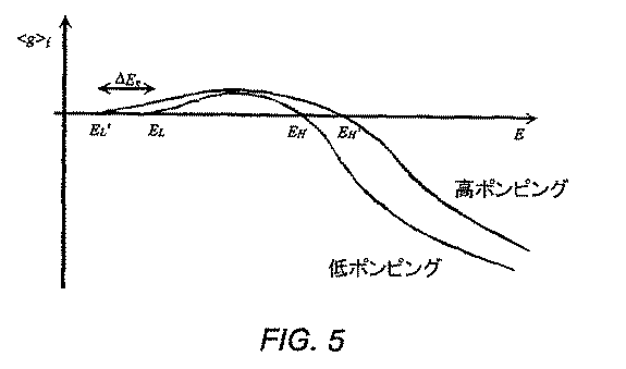
図4は、低キャリア注入レベル及び高キャリア注入レベル(即ち、低及び高ポンピング)における帯域構造体400を示している。SCH領域におけるキャリアの立ち上がりに関係する望ましくない損失は、部分的には、相当な帯域縮小402、ΔESによるSCH内に存在し得る帯域から帯域への遷移に関係するモードゲインの僅かな増加によって補正されるが、この帯域縮小は、SCHバンドギャップを下げ、材料が反転される高キャリア密度において、レーザー放射波長範囲内に入れる。図4に示されているように、高注入レベルでは、キャリアは量子井戸からこぼれ出てSCH領域を満たす。これによって屈折率は変化する。しかし、帯域縮小402、ΔESは、SCHのバンドギャップをレーザー放射遷移エネルギー以下になるように動かす。都合の良い事に、伝導/価電子帯状態では、占有は、正味ゲインが生じるように反転される。これらの影響は、適切なバイアスにより最初の場所において受動的散乱損失のゲイン補正があるという事実と相まって、先行技術の設計によって可能な出力よりもかなり高い出力を生み出す。図4は、高ポンピングでの低及び高エネルギーレベル408、410に対して、低ポンピングでの低及び高エネルギーレベル404、406を示している。FIG. 4 shows a
図5及び図6は、本発明の基本的設計による典型的な部分のモードゲイン/損失特性を更に詳細に説明している。図4に示されているのと同じ2つのポンピングレベルが考慮されている。図5は、図4のキャリア密度での、モードゲインとエネルギーとの関係を示している。図6は、モード指標とキャリア密度との関係を示している。 FIGS. 5 and 6 illustrate in more detail the mode gain / loss characteristics of an exemplary portion according to the basic design of the present invention. The same two pumping levels as shown in FIG. 4 are considered. FIG. 5 shows the relationship between mode gain and energy at the carrier density of FIG. FIG. 6 shows the relationship between the mode index and the carrier density.
図5は、図4の2つのポンピングレベルでのゲインを表している。第1は緩慢なポンピングであり、全部分が等しくポンピングされるのであれば、中心波長に閾値モードのゲインレベルを提供するには通常十分である。能動的ゲインは低エネルギー404、EL、即ち乱されていないサブバンドエッジのエネルギー分離から、高エネルギー406、EHまで伸張しており、即ち、SCHの伝導帯域エッジ(SCH内のキャリアの大きなパーセンテージを示唆している)から、量子井戸バリアよりはまだ下の或る価電子帯エネルギーまで伸張している。SCH内のキャリアの大きなパーセンテージでは、量子井戸内のキャリア密度はなおかなり高いことを理解することが重要である。つまり、モードの指標調整、従って波長調整は、図6に示すようにまだ小さい。第2の曲線は、高ポンピングでのゲインを示している。キャリアのクランピングを避けるためには何処かでポンピングを僅かに減らす必要があるが、図示のように、何れの波長にもゲインの増加はほとんどないので、これは必要ないかもしれない。重要なのは、SCHのキャリア密度の方が遙かに高いということであり、このことが、図6に示すように相当な調整をを提供している。ゲインスペクトルは、低エネルギー408、EL' から高エネルギー410、EH' までかなり広げられているが、レーザー放射帯域内で利用可能な状態の飽和により、そのピークでは殆ど増加していない。FIG. 5 represents the gain at the two pumping levels of FIG. The first is slow pumping, and if all parts are pumped equally, it is usually sufficient to provide a threshold mode gain level at the center wavelength. The active gain extends from the
図5のゲイン特性は、更に、この構成の飽和出力が大きいことも示している。例えば、参考文献としてここに援用するが、1995年、Lコールドレン及びSコルツィンによる「ダイオードレーザー及び光子集積回路」の第8章の式(8.18)から(8.24)のような様々な研究に見られるように、光学出力Pに対する増加ゲインgの飽和特性は、 The gain characteristic of FIG. 5 further shows that the saturation output of this configuration is large. For example, although incorporated herein by reference, various expressions such as equations (8.18) to (8.24) in Chapter 8 of “Diode Laser and Photon Integrated Circuits” by L Coldren and S Cortin in 1995. As seen in various studies, the saturation characteristic of the increase gain g with respect to the optical output P is
パラメータw及びdは、キャリアを含んでいる能動領域の幅及び厚さであり、(hν)は光子エネルギーであり、aは微分ゲインdg/dNであり、ΓXYは相対ゲイン/光学モードの重なりを測定する横方向閉じ込め係数であり、τはキャリアの寿命である。キャリアが、SCH領域へこぼれ出て図5に示す特性を呈すると、微分ゲインaは小さく(最良の量子井戸ゲイン領域の20%未満)なって、キャリアを含む厚さdは閉じ込め係数ΓXYよりも増える。従って、飽和出力は数回に渡り増加し、出力が数十ミリワットまで可能となる。Parameters w and d are the width and thickness of the active region containing the carrier, (hν) is the photon energy, a is the differential gain dg / dN, and Γ XY is the relative gain / optical mode overlap. Is the lateral confinement factor, and τ is the carrier lifetime. When carriers spill into the SCH region and exhibit the characteristics shown in FIG. 5, the differential gain a is small (less than 20% of the best quantum well gain region), and the thickness d including the carrier is determined by the confinement factor Γ XY . Will also increase. Therefore, the saturated output increases several times, and the output can be up to several tens of milliwatts.
図7は、別の実施例にある混合部分(又は選択的エリア成長又は突き合わせ接合再成長により形成された部分)のバンド構造体700を示しており、ミラー及び/又は位相偏移領域内のバンドギャップ内に変化が生まれている。最初の成長は、能動領域をより良好に最適化するために、より高いバンドギャップSCHで始まっている。混合の後、量子井戸のバンドギャップは上げられ、SCHのバンドギャップ702は僅かに下げられて、ゲイン及び調整の両方の部分の更なる最適作動が提供される。この場合の開始時材料の典型的なSCHバンドギャップ値は、1.45から1.4μmであろう。混合構造体700のSCHバンドギャップ702は、非混合構造体300のSCHバンドギャップよりも大きい。 FIG. 7 shows a
本発明の更に別の実施例は、何れかの部分のキャリア密度、並びに各部分へ少なくとも透明になるまでバイアスを掛ける必要性を変えるために、ゲインクランピングの自由度への影響を減じている。この場合、装置は先行技術によるSGDBRレーザーと同じように作動するが、我々がなお自由キャリア吸収の損失補正を測定できる点で大きく異なっている。このことは、不規則化量子井戸領域が、レーザー放出波長帯域の中心よりも多いバンドギャップ1−2kTを有している場合に起こる。従って、より多数のキャリアが注入される高ポンピングレベルでは、帯域縮小は、SCHのバンドエッジを、帯域から帯域への遷移がSCH内でレーザー放出波長で可能となるレベルまで下げる。このように、混合のないゲイン領域では、幾分か高いバンドギャップSCH領域が存在して、より良好なキャリア閉じ込めを提供し、一方、混合領域では、高ポンピングレベルでの所望の損失補正がなお存在する。従って、様々な部分の望ましい個々の特性に妥協は少ない。 Yet another embodiment of the present invention reduces the impact on gain clamping freedom to change the carrier density of any part and the need to bias each part at least until it is transparent. . In this case, the device works in the same way as a prior art SGDBR laser, but differs greatly in that we can still measure the loss correction for free carrier absorption. This occurs when the disordered quantum well region has a larger band gap of 1-2 kT than the center of the laser emission wavelength band. Thus, at high pumping levels where more carriers are injected, band reduction reduces the band edge of the SCH to a level where band-to-band transitions are possible at the laser emission wavelength in the SCH. Thus, in the unmixed gain region, there is a somewhat higher bandgap SCH region that provides better carrier confinement, while in the mixed region the desired loss correction at high pumping levels is still present. Exists. Thus, there are few compromises on the desired individual characteristics of the various parts.
図8A−8Bは、3つの異なるバンドギャップ領域が作られている実施例を示している。2つの下部バンドギャップ領域802は、図8Aに示すように、SGDBRミラー部106、108内に周期的に配置されている。図8Bは、SGDBRミラー部106、108内に配置されているそれらの内の2つとの可能な個々の電気的接続を示している。ゲイン部804と位相部806との電気的接点が代表例で示されている。フロント及びバックミラー108、106は、それぞれ、調整接点812、814と組み合わせられているゲイン接点808、810を有している。これは必須ではないが、各ミラー内に追加の電流ポートを有する犠牲を払うことにはなるが、より最適化された動作を提供する。ここで、ゲイン部内のSCH領域は、更に大きいバンドギャップ(1.3−1.4μm)と、この部分の最も効率的な動作に合わせて最適化されている量子井戸を有することができ、第1不規則化領域(第2バンドギャップ)は、量子井戸を混合してバンドギャップを僅かに増加させ、SCHを僅かに減少させる。更に、キャリア閉じ込めの量も、少なくとも倍増される。この領域は、ミラー内のゲインのために用いられる。この領域は、最適化された量子井戸ゲイン領域材料よりも幾らか高い飽和出力を有するであろうし、しかも、波長帯域の大部分に亘って良好なゲイン特性を有するであろうから、このことは望ましい。バンドギャップ縮小は、最適化された非混合ゲイン部と比べて良好なゲインを提供するのに高いキャリア密度が必要となるので、このことを可能にする。第2不規則化領域(第3バンドギャップ)は、十分に量子井戸とSCHを混合し、最適な調整特性を提供するが、損失は補正されない。部分的に混合されたゲイン領域は、ミラー内に周期的に配置され、比較的高い飽和出力によって損失補正を提供する。 8A-8B show an embodiment in which three different bandgap regions are created. The two lower
当業者には自明なように、本発明の上記実施例の原理は、公開譲渡され且つ同時係属中の以下の米国実用特許出願、即ち2000年7月12日出願の、ラリーAコールドレン他による第09/614,224号「統合型光学増幅器を備えた調整可能なレーザーソースを作る方法」と、2000年7月12日出願の、ラリーAコールドレンによる第09/614,377号「統合型光電子波長変換器アッセンブリ」と、2000年7月12日出願の、ラリーAコールドレン他による第09/614,376号「統合型変調器を備えた光電子レーザーによって光の波長を変える方法」と、2000年7月12日出願の、ラリーAコールドレン他による第09/614,378号「統合型変調器を備えた光電子レーザー」と、2000年7月12日出願の、ラリーAコールドレンによる第09/614,895号「一体式波長変換器アッセンブリを使って光の波長を変換するための方法」と、2000年7月12日出願の、ラリーAコールドレン他による第09/614,375号「統合型光学増幅器を備えた調整可能なレーザーソース」と、2000年7月12日出願の、ラリーAコールドレン他による第09/614,195号「統合型変調器を備えた光電子レーザーを作る方法」と、2000年7月12日出願のラリーAコールドレン他による第09/614,665号「統合型光学増幅器を備えた調整可能なレーザーソースによって光信号を生成する方法」と、2000年7月12日出願の、ラリーAコールドレンによる第09/614,674号「一体式波長変換器アッセンブリを作るための方法」に記載されているように、最適化された統合増幅器及び変調器を作成するのにも用いることができ、これら全てを参考文献としてここに援用するが、これら全ては互いに他の一部継続出願となっており、且つこれらは全て、35U.S.C.§119(e)の下に、以下の米国仮特許出願、即ち、1999年9月2日出願の、グレゴリー・フィッシュ他による、第60/152,038号「統合型変調器を備えた光電子レーザー」と、1999年9月2日出願の、ラリー・コールドレンによる、第60/152,049号「統合型光電子波長変換器」と、1999年9月2日出願の、ベック・メイソン他による、第60/152,072号「統合型光学増幅器を備えた調整可能なレーザーソース」に恩典を請求するものである。 As will be apparent to those skilled in the art, the principles of the above embodiments of the present invention are described in the following commonly assigned and co-pending U.S. utility patent application, filed July 12, 2000 by Larry A. Caldren et al. 09 / 614,224 “How to make a tunable laser source with integrated optical amplifier” and 09 / 614,377 by Larry A Caldren, filed July 12, 2000, “Integrated. Photoelectron wavelength converter assembly ", 09 / 614,376, filed July 12, 2000, by Larry A. Caldren et al." Method of changing the wavelength of light with an optoelectronic laser with an integrated modulator ", No. 09 / 614,378 “Photoelectron Laser with Integrated Modulator”, filed July 12, 2000 by Larry A. Caldren et al., July 12, 2000 No. 09 / 614,895, “Method for converting wavelength of light using an integrated wavelength converter assembly” by Larry A Caldren, and Larry A Cold Drain, filed July 12, 2000. No. 09 / 614,375 “Adjustable Laser Source with Integrated Optical Amplifier” and 09 / 614,195 by Larry A. Caldren et al. Method of making an optoelectronic laser with a modulator "and 09 / 614,665 by Larry A. Caldren et al., Filed July 12, 2000," Optical signal by an adjustable laser source with integrated optical amplifier. " ”And No. 09 / 614,674 by Larry A Coldren, filed July 12, 2000,“ Integrated Wavelength Converter Assembly ” Can also be used to create optimized integrated amplifiers and modulators, as described in "Methods for Making", all of which are incorporated herein by reference, all of which are Other partially continued applications, and all these are 35U. S. C. Under § 119 (e), the following US provisional patent application: 60 / 152,038 “Photoelectron Laser with Integrated Modulator” by Gregory Fish et al., Filed Sep. 2, 1999. ”60 / 152,049“ integrated optoelectronic wavelength converter ”filed September 2, 1999, by Larry Coldren, and Beck Mason et al. Filed September 2, 1999, No. 60 / 152,072 “Adjustable laser source with integrated optical amplifier”.
これは、本発明の好適な実施例の説明を結論付けている。要約すれば、本発明は、ある帯域幅に亘って誘発された放出及び自発的な放出により光線を作り出すためのゲイン部と、前記光線を前記帯域幅の中心周波数の周りに制御するための位相部と、比較的低エネルギーバンドギャップの分離閉じ込めヘテロ構造(SCH)を含んでいる空洞内で光線を案内し反射するための導波管と、前記空洞の一方の端部の境界を成すフロントミラーと、前記空洞の反対側の端部の境界を成すバックミラーとを備え、ゲインは、位相部、フロントミラー及びバックミラーから成るグループの内の少なくとも1つによって提供されるようになっている調整可能なレーザーを開示している。 This concludes the description of the preferred embodiment of the present invention. In summary, the present invention provides a gain section for producing a light beam by emission induced and spontaneous emission over a bandwidth, and a phase for controlling the light beam around a center frequency of the bandwidth. , A waveguide for guiding and reflecting light rays in a cavity containing a separate confinement heterostructure (SCH) with a relatively low energy bandgap, and a front mirror bounding one end of the cavity And a rearview mirror delimiting the opposite end of the cavity, the gain being provided by at least one of the group consisting of a phase portion, a front mirror and a rearview mirror A possible laser is disclosed.
本発明の1つ又は複数の実施例に関する上記記述は、解説と説明を目的として提示されている。本発明を、開示している形態そのもので網羅したり、これに限定する意図はない。上記教示に照らして、多くの修正及び変更が可能である。本発明の範囲は、この詳細な説明ではなく、請求の範囲に述べる事項によって限定されるものである。 The foregoing description of one or more embodiments of the present invention has been presented for purposes of illustration and description. It is not intended to be exhaustive or to limit the invention to the precise form disclosed. Many modifications and variations are possible in light of the above teaching. It is intended that the scope of the invention be limited not by this detailed description, but rather by the subject matter recited in the claims.
Claims (20)
光線を案内するための導波管であって、前記光線にゲインを提供するのに十分な低いエネルギーバンドギャップを有する分離閉じ込めへテロ構造(SCH)を含んでいる導波管を備え、
前記導波管が、空洞を含み、
前記空洞が、
該空洞内にあって、前記光線の自然放出を行うと共に前記光線にゲインを提供するためのゲイン部と、
該空洞内にあって、前記光線を或る帯域幅の中心周波数の周りに調整するための位相部と、を有し、
前記導波管内にあって、前記空洞の一方の端部を定めるフロントミラーを備え、
前記導波管内にあって、前記空洞の反対側の端部を定めるバックミラーを備え、
前記ゲイン部は、量子井戸バンドギャップとSCHバンドギャップを有し、前記量子井戸バンドギャップは、前記SCHバンドギャップよりも小さく、
前記SCHを含んでいる前記導波管は、前記ゲイン部、前記位相部、前記フロントミラー及び前記バックミラーに亘って均一であり、
前記レーザーは、レーザー放射閾値を有し、前記SCHは、該SCHの中心にあって前記レーザーがレーザー放射閾値に到達したときに満たされるのに十分な浅い量子井戸を含んでおり、
動作時に、前記位相部、前記フロントミラー及び前記バックミラーの少なくとも1つによって前記光線に更なるゲインが提供され、前記調整に関連する損失が相殺されることを特徴とするレーザー。
In the tunable laser,
A waveguide for guiding a light beam comprising a separate confinement heterostructure (SCH) having a low energy band gap sufficient to provide gain to the light beam;
The waveguide includes a cavity;
The cavity is
A gain section in the cavity for spontaneous emission of the light beam and providing gain to the light beam;
A phase portion within the cavity for adjusting the light beam around a center frequency of a bandwidth;
A front mirror in the waveguide and defining one end of the cavity;
A rearview mirror in the waveguide and defining an opposite end of the cavity;
The gain section has a quantum well band gap and an SCH band gap, and the quantum well band gap is smaller than the SCH band gap,
The waveguide containing the SCH is uniform across the gain section, the phase section, the front mirror and the rearview mirror;
The laser has a laser emission threshold, and the SCH includes a quantum well that is at the center of the SCH and is shallow enough to be filled when the laser reaches the laser emission threshold;
In operation, at least one of the phase portion, the front mirror, and the rearview mirror provides additional gain to the light beam to offset the loss associated with the adjustment.
The laser of claim 1, wherein in operation, the gain provided by at least one of the phase portion, the front mirror, and the rearview mirror has a saturation power substantially higher than 5 mW.
The laser of claim 1, wherein the SCH is optimized such that the gain quickly increases to a level substantially equal to that required for a device threshold.
2. The gain unit, the phase unit, the front mirror, and the rearview mirror each have a refractive index that is individually adjusted by a bias that is individually changed. laser.
The laser of claim 1, wherein the refractive index is adjusted while maintaining a net gain at a device threshold.
A free carrier absorption loss resulting from an increase in carrier density in the SCH is at least partially corrected by a gain provided by the at least one of the phase portion, the front mirror, and the rearview mirror. The laser according to claim 1.
The gain according to claim 1, wherein the gain provided by at least one of the phase portion, the front mirror, and the rearview mirror is multiplied through an electrical contact combined with an adjustment electrical contact. laser.
光線を案内するための導波管層を成長させる段階を備え、前記導波管層が、前記光線にゲインを提供するのに十分な低いエネルギーバンドギャップを有する分離閉じ込めへテロ構造(SCH)領域を基板上に含んでおり、
前記導波管層が、空洞を含み、
前記空洞が、
該空洞内にあって、前記光線の自然放出を行うと共に前記光線にゲインを提供するためのゲイン部と、
該空洞内にあって、前記光線を或る帯域幅の中心周波数の周りに調整するための位相部と、を有し、
前記導波管層内に抽出された格子溝をエッチングして、前記導波管内で前記空洞の一方の端部を定めるフロントミラーと、前記導波管内で前記空洞の反対側の端部を定めるバックミラーとを形成する段階を備え、
前記導波管層上に上部クラッディング及び接点層を成長させる段階を備え、
前記ゲイン部は、量子井戸バンドギャップとSCHバンドギャップを有し、前記量子井戸バンドギャップは、前記SCHバンドギャップよりも小さく、
前記SCHを含んでいる前記導波管は、前記ゲイン部、前記位相部、前記フロントミラー及び前記バックミラーに亘って均一であり、
前記レーザーは、レーザー放射閾値を有し、前記SCHは、該SCHの中心にあって前記レーザーがレーザー放射閾値に到達したときに満たされるのに十分な浅い量子井戸を含んでおり、
動作時に、前記位相部、前記フロントミラー及び前記バックミラーの少なくとも1つによって前記光線に更なるゲインが提供され、前記調整に関連する損失が相殺されることを特徴とする方法。
In a method of manufacturing a semiconductor laser,
Growing a waveguide layer for guiding the light beam, wherein the waveguide layer has a low energy band gap sufficient to provide gain to the light beam; On the substrate,
The waveguide layer includes a cavity;
The cavity is
A gain section in the cavity for spontaneous emission of the light beam and providing gain to the light beam;
A phase portion within the cavity for adjusting the light beam around a center frequency of a bandwidth;
Etching the extracted grating grooves in the waveguide layer to define one end of the cavity in the waveguide and defining the opposite end of the cavity in the waveguide Comprising the step of forming a rearview mirror,
Growing an upper cladding and contact layer on the waveguide layer;
The gain section has a quantum well band gap and an SCH band gap, and the quantum well band gap is smaller than the SCH band gap,
The waveguide containing the SCH is uniform across the gain section, the phase section, the front mirror and the rearview mirror;
The laser has a laser emission threshold, and the SCH includes a quantum well that is at the center of the SCH and is shallow enough to be filled when the laser reaches the laser emission threshold;
In operation, the gain is provided to the light beam by at least one of the phase portion, the front mirror and the back mirror to cancel the loss associated with the adjustment.
9. The method of claim 8 , wherein the SCH is optimized such that the gain quickly increases to a level substantially equal to that required for a device threshold.
The gain provided by the at least one of the phase portion, the front mirror and the rearview mirror comprises selective quantum well mixing, selective area growth, and butt-junction regrowth of different bandgap waveguides. 9. The method of claim 8 , wherein the method is modified by a process selected from a group.
Gain is provided by two or more of the group consisting of the phase portion, the front mirror, and the back mirror, each gain for selective quantum well mixing, selective area growth, and different bandgap waveguides. 9. The method of claim 8 , wherein the method is individually modified by a process selected from the group consisting of butt joint regrowth.
Gain is provided by the front mirror that is modified by selective quantum well mixing, and gain is provided by the rearview mirror that is modified by selective quantum well mixing, each mixture creating a different bandgap region. The method according to claim 11 .
The phase portion, the front mirror, and the rearview mirror each have a quantum well band gap and an SCH band gap, and the quantum well band gap of the gain portion is the lowest among all the band gaps. The method according to claim 11 , wherein the SCH band gap is the highest.
光線を案内するための導波管であって、前記光線にゲインを提供するのに十分な低いエネルギーバンドギャップを有する分離閉じ込めへテロ構造(SCH)を含んでいる導波管を備え、
前記導波管が、空洞を含み、
前記空洞が、
該空洞内にあって、前記光線の自然放出を行うと共に前記光線にゲインを提供するためのゲイン部と、
該空洞内にあって、前記光線を或る帯域幅の中心周波数の周りに調整するための位相部と、を有し、
前記導波管内にあって、前記空洞の一方の端部を定めるフロントミラーを備え、
前記導波管内にあって、前記空洞の反対側の端部を定めるバックミラーを備え、
前記ゲイン部は、量子井戸バンドギャップとSCHバンドギャップを有し、前記量子井戸バンドギャップは、前記SCHバンドギャップよりも小さく、
前記SCHを含んでいる前記導波管は、前記ゲイン部、前記位相部、前記フロントミラー及び前記バックミラーに亘って均一であり、
前記レーザーは、レーザー放射閾値を有し、前記SCHは、該SCHの中心にあって前記レーザーがレーザー放射閾値に到達したときに満たされるのに十分な浅い量子井戸を含んでおり、
動作時に、前記位相部、前記フロントミラー及び前記バックミラーの少なくとも1つによって前記光線に更なるゲインが提供され、前記調整に関連する損失が相殺されることを特徴とする製品。
In a product equipped with an extraction grating dispersion type Bragg reflector (SGDBR) laser, the SGDBR laser is:
A waveguide for guiding a light beam comprising a separate confinement heterostructure (SCH) having a low energy band gap sufficient to provide gain to the light beam;
The waveguide includes a cavity;
The cavity is
A gain section in the cavity for spontaneous emission of the light beam and providing gain to the light beam;
A phase portion within the cavity for adjusting the light beam around a center frequency of a bandwidth;
A front mirror in the waveguide and defining one end of the cavity;
A rearview mirror in the waveguide and defining an opposite end of the cavity;
The gain section has a quantum well band gap and an SCH band gap, and the quantum well band gap is smaller than the SCH band gap,
The waveguide containing the SCH is uniform across the gain section, the phase section, the front mirror and the rearview mirror;
The laser has a laser emission threshold, and the SCH includes a quantum well that is at the center of the SCH and is shallow enough to be filled when the laser reaches the laser emission threshold;
In operation, at least one of the phase portion, the front mirror and the rearview mirror provides additional gain to the light beam to offset the loss associated with the adjustment.
15. The gain of claim 14 , wherein in operation, the gain provided by at least one of the phase portion, the front mirror and the rearview mirror has a saturation power substantially higher than 5 mW. Product.
15. A product as claimed in claim 14 , characterized in that the SCH is optimized so that the gain increases rapidly to a level substantially equal to that required for a device threshold.
15. The gain unit according to claim 14 , wherein each of the gain unit, the phase unit, the front mirror, and the rearview mirror has a refractive index that is individually adjusted by a bias that is individually changed. Product.
18. Product according to claim 17 , characterized in that the refractive index is adjusted while maintaining a net gain at the device threshold.
Free carrier absorption loss resulting from an increase in carrier density in the SCH is corrected at least in part by a gain provided by at least one of the phase portion, the front mirror, and the rearview mirror. 15. A product according to claim 14 .
Applications Claiming Priority (21)
| Application Number | Priority Date | Filing Date | Title |
|---|---|---|---|
| US20906800P | 2000-06-02 | 2000-06-02 | |
| US60/209,068 | 2000-06-02 | ||
| US09/614,378 | 2000-07-12 | ||
| US09/614,195 US6574259B1 (en) | 1999-09-02 | 2000-07-12 | Method of making an opto-electronic laser with integrated modulator |
| US09/614,375 | 2000-07-12 | ||
| US09/614,895 US6349106B1 (en) | 1999-09-02 | 2000-07-12 | Method for converting an optical wavelength using a monolithic wavelength converter assembly |
| US09/614,195 | 2000-07-12 | ||
| US09/614,224 | 2000-07-12 | ||
| US09/614,674 | 2000-07-12 | ||
| US09/614,665 | 2000-07-12 | ||
| US09/614,376 US6614819B1 (en) | 1999-09-02 | 2000-07-12 | Method of modulating an optical wavelength with an opto-electronic laser with integrated modulator |
| US09/614,665 US6687278B1 (en) | 1999-09-02 | 2000-07-12 | Method of generating an optical signal with a tunable laser source with integrated optical amplifier |
| US09/614,377 | 2000-07-12 | ||
| US09/614,375 US6658035B1 (en) | 1999-09-02 | 2000-07-12 | Tunable laser source with integrated optical amplifier |
| US09/614,224 US6654400B1 (en) | 1999-09-02 | 2000-07-12 | Method of making a tunable laser source with integrated optical amplifier |
| US09/614,674 US6624000B1 (en) | 1999-09-02 | 2000-07-12 | Method for making a monolithic wavelength converter assembly |
| US09/614,895 | 2000-07-12 | ||
| US09/614,377 US6580739B1 (en) | 1999-09-02 | 2000-07-12 | Integrated opto-electronic wavelength converter assembly |
| US09/614,378 US6628690B1 (en) | 1999-09-02 | 2000-07-12 | Opto-electronic laser with integrated modulator |
| US09/614,376 | 2000-07-12 | ||
| PCT/US2001/017884 WO2001095444A2 (en) | 2000-06-02 | 2001-06-01 | High-power sampled grating distributed bragg reflector lasers |
Publications (2)
| Publication Number | Publication Date |
|---|---|
| JP2003536264A JP2003536264A (en) | 2003-12-02 |
| JP5443660B2 true JP5443660B2 (en) | 2014-03-19 |
Family
ID=27581149
Family Applications (1)
| Application Number | Title | Priority Date | Filing Date |
|---|---|---|---|
| JP2002502873A Expired - Lifetime JP5443660B2 (en) | 2000-06-02 | 2001-06-01 | High output, manufacturable extraction grating dispersed Bragg reflector laser |
Country Status (8)
| Country | Link |
|---|---|
| EP (1) | EP1290765B1 (en) |
| JP (1) | JP5443660B2 (en) |
| CN (1) | CN1227789C (en) |
| AT (1) | ATE274760T1 (en) |
| AU (1) | AU2001266663A1 (en) |
| CA (1) | CA2410964C (en) |
| DE (1) | DE60105154T2 (en) |
| WO (1) | WO2001095444A2 (en) |
Families Citing this family (20)
| Publication number | Priority date | Publication date | Assignee | Title |
|---|---|---|---|---|
| US7286585B2 (en) | 1998-12-21 | 2007-10-23 | Finisar Corporation | Low temperature grown layers with migration enhanced epitaxy adjacent to an InGaAsN(Sb) based active region |
| US6975660B2 (en) | 2001-12-27 | 2005-12-13 | Finisar Corporation | Vertical cavity surface emitting laser including indium and antimony in the active region |
| US7257143B2 (en) | 1998-12-21 | 2007-08-14 | Finisar Corporation | Multicomponent barrier layers in quantum well active regions to enhance confinement and speed |
| US7167495B2 (en) | 1998-12-21 | 2007-01-23 | Finisar Corporation | Use of GaAs extended barrier layers between active regions containing nitrogen and AlGaAs confining layers |
| US20030219917A1 (en) | 1998-12-21 | 2003-11-27 | Johnson Ralph H. | System and method using migration enhanced epitaxy for flattening active layers and the mechanical stabilization of quantum wells associated with vertical cavity surface emitting lasers |
| US7408964B2 (en) | 2001-12-20 | 2008-08-05 | Finisar Corporation | Vertical cavity surface emitting laser including indium and nitrogen in the active region |
| US7095770B2 (en) | 2001-12-20 | 2006-08-22 | Finisar Corporation | Vertical cavity surface emitting laser including indium, antimony and nitrogen in the active region |
| US7058112B2 (en) | 2001-12-27 | 2006-06-06 | Finisar Corporation | Indium free vertical cavity surface emitting laser |
| US6922426B2 (en) | 2001-12-20 | 2005-07-26 | Finisar Corporation | Vertical cavity surface emitting laser including indium in the active region |
| US7435660B2 (en) | 1998-12-21 | 2008-10-14 | Finisar Corporation | Migration enhanced epitaxy fabrication of active regions having quantum wells |
| US7295586B2 (en) | 2002-02-21 | 2007-11-13 | Finisar Corporation | Carbon doped GaAsSb suitable for use in tunnel junctions of long-wavelength VCSELs |
| US6822995B2 (en) | 2002-02-21 | 2004-11-23 | Finisar Corporation | GaAs/AI(Ga)As distributed bragg reflector on InP |
| GB0206204D0 (en) * | 2002-03-15 | 2002-05-01 | Denselight Semiconductors Pte | Direct modulation of laser diode with chirp control |
| US7860137B2 (en) | 2004-10-01 | 2010-12-28 | Finisar Corporation | Vertical cavity surface emitting laser with undoped top mirror |
| CN101432936B (en) | 2004-10-01 | 2011-02-02 | 菲尼萨公司 | Vertical cavity surface emitting laser having multiple top-side contacts |
| CN100377453C (en) * | 2006-05-12 | 2008-03-26 | 何建军 | Q-modulation semiconductor laser with electric absorption grating structure |
| JP2008263216A (en) * | 2008-06-03 | 2008-10-30 | Matsushita Electric Ind Co Ltd | Semiconductor laser and manufacturing method thereof |
| CN102044844B (en) * | 2010-11-24 | 2012-05-23 | 中国科学院半导体研究所 | Distributed Amplified Sampled Grating Distributed Bragg Reflection Tunable Laser |
| US8908734B2 (en) * | 2012-05-17 | 2014-12-09 | Finisar Corporation | Directly modulated laser for PON applications |
| US10231038B2 (en) * | 2014-02-24 | 2019-03-12 | Rockley Photonics Limited | Detector remodulator and optoelectronic switch |
Family Cites Families (17)
| Publication number | Priority date | Publication date | Assignee | Title |
|---|---|---|---|---|
| JPS60145686A (en) * | 1984-01-09 | 1985-08-01 | Nec Corp | Semiconductor laser |
| JPS60145687A (en) * | 1984-01-09 | 1985-08-01 | Nec Corp | Semiconductor laser |
| JPS6414988A (en) * | 1987-07-08 | 1989-01-19 | Nec Corp | Wavelength-tunable semiconductor laser |
| JPH0626268B2 (en) * | 1987-08-19 | 1994-04-06 | 日本電気株式会社 | Tunable semiconductor laser |
| JPH0636460B2 (en) * | 1988-12-21 | 1994-05-11 | 光計測技術開発株式会社 | Method for manufacturing semiconductor optical integrated circuit |
| JPH02211686A (en) * | 1989-02-13 | 1990-08-22 | Mitsubishi Electric Corp | Semiconductor laser |
| US5088097A (en) * | 1990-04-04 | 1992-02-11 | Canon Kabushiki Kaisha | Semiconductor laser element capable of changing emission wavelength, and method of driving the same |
| JPH0439985A (en) * | 1990-06-05 | 1992-02-10 | Fujitsu Ltd | Light beam deflector |
| JP2913922B2 (en) * | 1991-08-09 | 1999-06-28 | 日本電気株式会社 | Quantum well distributed feedback semiconductor laser |
| JPH0555689A (en) * | 1991-08-23 | 1993-03-05 | Nippon Telegr & Teleph Corp <Ntt> | Distributed reflection type semiconductor laser with wavelength control function |
| JP2832920B2 (en) * | 1992-03-06 | 1998-12-09 | 日本電信電話株式会社 | Semiconductor laser with wavelength sweep function |
| JP3226073B2 (en) * | 1994-02-18 | 2001-11-05 | キヤノン株式会社 | Semiconductor laser capable of polarization modulation and its use |
| US5841799A (en) * | 1994-12-17 | 1998-11-24 | Canon Kabushiki Kaisha | Semiconductor laser, modulation method therefor and optical communication system using the same |
| JP2877107B2 (en) * | 1996-12-02 | 1999-03-31 | 日本電気株式会社 | Multiple quantum well semiconductor laser |
| JPH10117046A (en) * | 1996-08-22 | 1998-05-06 | Canon Inc | Semiconductor laser, driving method thereof, optical transmitter using the same, and optical communication system using the same |
| JPH10256675A (en) * | 1997-03-14 | 1998-09-25 | Canon Inc | Tunable semiconductor laser, method of driving the same, and optical communication system using the same |
| EP1172905A1 (en) * | 2000-07-11 | 2002-01-16 | Interuniversitair Microelektronica Centrum Vzw | A method and apparatus for controlling a laser structure |
-
2001
- 2001-06-01 CN CN01810499.1A patent/CN1227789C/en not_active Expired - Lifetime
- 2001-06-01 DE DE60105154T patent/DE60105154T2/en not_active Expired - Lifetime
- 2001-06-01 WO PCT/US2001/017884 patent/WO2001095444A2/en not_active Ceased
- 2001-06-01 JP JP2002502873A patent/JP5443660B2/en not_active Expired - Lifetime
- 2001-06-01 EP EP01944233A patent/EP1290765B1/en not_active Expired - Lifetime
- 2001-06-01 CA CA2410964A patent/CA2410964C/en not_active Expired - Fee Related
- 2001-06-01 AU AU2001266663A patent/AU2001266663A1/en not_active Abandoned
- 2001-06-01 AT AT01944233T patent/ATE274760T1/en not_active IP Right Cessation
Also Published As
| Publication number | Publication date |
|---|---|
| JP2003536264A (en) | 2003-12-02 |
| WO2001095444A3 (en) | 2002-06-20 |
| WO2001095444A2 (en) | 2001-12-13 |
| CA2410964A1 (en) | 2001-12-13 |
| CN1227789C (en) | 2005-11-16 |
| EP1290765B1 (en) | 2004-08-25 |
| CN1432207A (en) | 2003-07-23 |
| CA2410964C (en) | 2010-11-30 |
| DE60105154T2 (en) | 2005-09-08 |
| ATE274760T1 (en) | 2004-09-15 |
| AU2001266663A1 (en) | 2001-12-17 |
| DE60105154D1 (en) | 2004-09-30 |
| EP1290765A2 (en) | 2003-03-12 |
Similar Documents
| Publication | Publication Date | Title |
|---|---|---|
| JP5443660B2 (en) | High output, manufacturable extraction grating dispersed Bragg reflector laser | |
| US6256330B1 (en) | Gain and index tailored single mode semiconductor laser | |
| US6563631B2 (en) | Tunable gain-clamped semiconductor optical amplifier | |
| US5936994A (en) | Two-section complex coupled distributed feedback semiconductor laser with enhanced wavelength tuning range | |
| US20050053112A1 (en) | Surface emitting dfb laser structures for broadband communication systems and array of same | |
| US20020114367A1 (en) | Quantum dot lasers | |
| US8073033B2 (en) | Optical semiconductor device and driving method thereof | |
| US6909734B2 (en) | High-power, manufacturable sampled grating distributed Bragg reflector lasers | |
| EP0661783B1 (en) | Method for fabricating semiconductor light integrated circuit | |
| JP2003046190A (en) | Semiconductor laser | |
| US5764682A (en) | Distributed feedback semiconductor laser and method for fabricating the same | |
| US5502741A (en) | Direct amplitude modulation of lasers | |
| CA2423782A1 (en) | Quantum dot lasers | |
| JP3149961B2 (en) | Multi-wavelength semiconductor laser device and driving method thereof | |
| JP2002111125A (en) | Distributed feedback semiconductor laser | |
| JP7265198B2 (en) | Tunable DBR semiconductor laser | |
| JP3149959B2 (en) | Semiconductor laser device and driving method thereof | |
| JP3149962B2 (en) | Multi-wavelength semiconductor laser device and driving method thereof | |
| US5317588A (en) | Ridge waveguide distributed-feedback laser diode with a depressed-index cladding layer | |
| JP2001237494A (en) | Semiconductor laser device | |
| JP2703618B2 (en) | Semiconductor laser device | |
| JP3303632B2 (en) | Semiconductor optical device and manufacturing method thereof | |
| JPH09214059A (en) | Semiconductor optical device using quantum wire, light source device using the same, optical communication system, and optical communication system | |
| Duan et al. | Tunable photonic crystal lasers with high side-mode suppression ratio | |
| Schreiner et al. | Monolithically integrated tunable laterally coupled distributed feedback lasers with self-aligned Ti/Pt/Au ohmic contacts |
Legal Events
| Date | Code | Title | Description |
|---|---|---|---|
| A621 | Written request for application examination |
Free format text: JAPANESE INTERMEDIATE CODE: A621 Effective date: 20080526 |
|
| A711 | Notification of change in applicant |
Free format text: JAPANESE INTERMEDIATE CODE: A711 Effective date: 20080918 |
|
| A131 | Notification of reasons for refusal |
Free format text: JAPANESE INTERMEDIATE CODE: A131 Effective date: 20110530 |
|
| A977 | Report on retrieval |
Free format text: JAPANESE INTERMEDIATE CODE: A971007 Effective date: 20110601 |
|
| A521 | Request for written amendment filed |
Free format text: JAPANESE INTERMEDIATE CODE: A523 Effective date: 20110815 |
|
| A131 | Notification of reasons for refusal |
Free format text: JAPANESE INTERMEDIATE CODE: A131 Effective date: 20120820 |
|
| A521 | Request for written amendment filed |
Free format text: JAPANESE INTERMEDIATE CODE: A523 Effective date: 20121101 |
|
| A02 | Decision of refusal |
Free format text: JAPANESE INTERMEDIATE CODE: A02 Effective date: 20130610 |
|
| A521 | Request for written amendment filed |
Free format text: JAPANESE INTERMEDIATE CODE: A523 Effective date: 20131009 |
|
| A911 | Transfer to examiner for re-examination before appeal (zenchi) |
Free format text: JAPANESE INTERMEDIATE CODE: A911 Effective date: 20131017 |
|
| TRDD | Decision of grant or rejection written | ||
| A01 | Written decision to grant a patent or to grant a registration (utility model) |
Free format text: JAPANESE INTERMEDIATE CODE: A01 Effective date: 20131216 |
|
| A61 | First payment of annual fees (during grant procedure) |
Free format text: JAPANESE INTERMEDIATE CODE: A61 Effective date: 20131220 |
|
| R150 | Certificate of patent or registration of utility model |
Free format text: JAPANESE INTERMEDIATE CODE: R150 Ref document number: 5443660 Country of ref document: JP Free format text: JAPANESE INTERMEDIATE CODE: R150 |
|
| S111 | Request for change of ownership or part of ownership |
Free format text: JAPANESE INTERMEDIATE CODE: R313113 |
|
| S533 | Written request for registration of change of name |
Free format text: JAPANESE INTERMEDIATE CODE: R313533 |
|
| R350 | Written notification of registration of transfer |
Free format text: JAPANESE INTERMEDIATE CODE: R350 |
|
| R250 | Receipt of annual fees |
Free format text: JAPANESE INTERMEDIATE CODE: R250 |
|
| R250 | Receipt of annual fees |
Free format text: JAPANESE INTERMEDIATE CODE: R250 |
|
| R250 | Receipt of annual fees |
Free format text: JAPANESE INTERMEDIATE CODE: R250 |
|
| R250 | Receipt of annual fees |
Free format text: JAPANESE INTERMEDIATE CODE: R250 |
|
| R250 | Receipt of annual fees |
Free format text: JAPANESE INTERMEDIATE CODE: R250 |
|
| EXPY | Cancellation because of completion of term |