JP5386785B2 - Semiconductor device and manufacturing method thereof - Google Patents
Semiconductor device and manufacturing method thereof Download PDFInfo
- Publication number
- JP5386785B2 JP5386785B2 JP2007079229A JP2007079229A JP5386785B2 JP 5386785 B2 JP5386785 B2 JP 5386785B2 JP 2007079229 A JP2007079229 A JP 2007079229A JP 2007079229 A JP2007079229 A JP 2007079229A JP 5386785 B2 JP5386785 B2 JP 5386785B2
- Authority
- JP
- Japan
- Prior art keywords
- electrode
- semiconductor device
- layer
- insulating film
- compound semiconductor
- Prior art date
- Legal status (The legal status is an assumption and is not a legal conclusion. Google has not performed a legal analysis and makes no representation as to the accuracy of the status listed.)
- Active
Links
- 239000004065 semiconductor Substances 0.000 title claims description 207
- 238000004519 manufacturing process Methods 0.000 title claims description 24
- VYPSYNLAJGMNEJ-UHFFFAOYSA-N Silicium dioxide Chemical compound O=[Si]=O VYPSYNLAJGMNEJ-UHFFFAOYSA-N 0.000 claims description 48
- 229910052814 silicon oxide Inorganic materials 0.000 claims description 48
- 229910052581 Si3N4 Inorganic materials 0.000 claims description 47
- HQVNEWCFYHHQES-UHFFFAOYSA-N silicon nitride Chemical compound N12[Si]34N5[Si]62N3[Si]51N64 HQVNEWCFYHHQES-UHFFFAOYSA-N 0.000 claims description 47
- -1 nitride compound Chemical class 0.000 claims description 34
- 150000004767 nitrides Chemical class 0.000 claims description 28
- 150000001875 compounds Chemical class 0.000 claims description 27
- 229920001721 polyimide Polymers 0.000 claims description 19
- 239000009719 polyimide resin Substances 0.000 claims description 19
- 238000000034 method Methods 0.000 claims description 18
- 230000005533 two-dimensional electron gas Effects 0.000 claims description 9
- 230000008569 process Effects 0.000 claims description 7
- 239000012159 carrier gas Substances 0.000 claims description 4
- 238000010030 laminating Methods 0.000 claims description 4
- 239000010410 layer Substances 0.000 description 133
- 238000010586 diagram Methods 0.000 description 21
- 230000004888 barrier function Effects 0.000 description 18
- 238000007747 plating Methods 0.000 description 15
- 239000000758 substrate Substances 0.000 description 15
- 230000015556 catabolic process Effects 0.000 description 13
- 230000004048 modification Effects 0.000 description 13
- 238000012986 modification Methods 0.000 description 13
- 230000000694 effects Effects 0.000 description 11
- 230000005684 electric field Effects 0.000 description 10
- 239000011229 interlayer Substances 0.000 description 9
- 229910002704 AlGaN Inorganic materials 0.000 description 4
- 230000007423 decrease Effects 0.000 description 4
- 238000000059 patterning Methods 0.000 description 4
- 230000005669 field effect Effects 0.000 description 3
- 230000000116 mitigating effect Effects 0.000 description 3
- 238000004544 sputter deposition Methods 0.000 description 3
- 238000001771 vacuum deposition Methods 0.000 description 3
- XUIMIQQOPSSXEZ-UHFFFAOYSA-N Silicon Chemical compound [Si] XUIMIQQOPSSXEZ-UHFFFAOYSA-N 0.000 description 2
- 238000000137 annealing Methods 0.000 description 2
- 239000000919 ceramic Substances 0.000 description 2
- 229910052802 copper Inorganic materials 0.000 description 2
- 239000013078 crystal Substances 0.000 description 2
- 230000007547 defect Effects 0.000 description 2
- 238000009713 electroplating Methods 0.000 description 2
- 229910052737 gold Inorganic materials 0.000 description 2
- 238000009413 insulation Methods 0.000 description 2
- 229910021421 monocrystalline silicon Inorganic materials 0.000 description 2
- 238000000206 photolithography Methods 0.000 description 2
- 230000010287 polarization Effects 0.000 description 2
- 230000009467 reduction Effects 0.000 description 2
- 230000002040 relaxant effect Effects 0.000 description 2
- 230000000630 rising effect Effects 0.000 description 2
- 229910052710 silicon Inorganic materials 0.000 description 2
- 239000010703 silicon Substances 0.000 description 2
- HBMJWWWQQXIZIP-UHFFFAOYSA-N silicon carbide Chemical compound [Si+]#[C-] HBMJWWWQQXIZIP-UHFFFAOYSA-N 0.000 description 2
- 230000015572 biosynthetic process Effects 0.000 description 1
- 238000006243 chemical reaction Methods 0.000 description 1
- 239000002131 composite material Substances 0.000 description 1
- 230000006835 compression Effects 0.000 description 1
- 238000007906 compression Methods 0.000 description 1
- 230000003247 decreasing effect Effects 0.000 description 1
- 238000009422 external insulation Methods 0.000 description 1
- 230000007246 mechanism Effects 0.000 description 1
- 239000002184 metal Substances 0.000 description 1
- 229910052751 metal Inorganic materials 0.000 description 1
- 229910044991 metal oxide Inorganic materials 0.000 description 1
- 150000004706 metal oxides Chemical class 0.000 description 1
- 238000002161 passivation Methods 0.000 description 1
- 230000001681 protective effect Effects 0.000 description 1
- 230000001629 suppression Effects 0.000 description 1
Images


Landscapes
- Metal-Oxide And Bipolar Metal-Oxide Semiconductor Integrated Circuits (AREA)
- Junction Field-Effect Transistors (AREA)
- Thin Film Transistor (AREA)
- Insulated Gate Type Field-Effect Transistor (AREA)
- Electrodes Of Semiconductors (AREA)
Description
本発明は、半導体装置およびその製造方法に関し、特に、厚いソースフィールドプレート(FP:Field Plate)電極による応力緩和機構に特徴を有する半導体装置およびその製造方法に関する。 The present invention relates to a semiconductor device and a manufacturing method thereof, and more particularly to a semiconductor device characterized by a stress relaxation mechanism using a thick source field plate (FP) electrode and a manufacturing method thereof.
窒化物系化合物半導体を用いた半導体素子は高周波・高耐圧特性を有することから、近年注目されている。しかし、窒化物系化合物半導体を用いた半導体素子は高電圧動作時のドレイン電流の低下(いわゆる電流コラプス現象)やゲート漏れ電流の問題から、スイッチング素子などのパワーデバイスとしては実用化されていない。 In recent years, semiconductor elements using nitride-based compound semiconductors have attracted attention because of their high frequency and high breakdown voltage characteristics. However, a semiconductor device using a nitride-based compound semiconductor has not been put into practical use as a power device such as a switching device because of a problem of a decrease in drain current (so-called current collapse phenomenon) during high voltage operation and a gate leakage current.
その解決法の1つとして、ゲート電極の主部分(以下、ゲート電極)から延伸したフィールドプレート(FP)電極部分(以下、FP電極)をドレイン電極とゲート電極との間に設けた、窒化物系化合物半導体からなる半導体素子が開示されている。(例えば、特許文献1参照。)。 As one of the solutions, a nitride in which a field plate (FP) electrode portion (hereinafter referred to as FP electrode) extending from a main portion (hereinafter referred to as gate electrode) of the gate electrode is provided between the drain electrode and the gate electrode. A semiconductor device made of a compound semiconductor is disclosed. (For example, refer to Patent Document 1).
特許文献1では、ゲート電極を跨ぐように、ゲート電極と絶縁膜を介して、ソース電極と電気的に接続したソースFP電極をドレイン電極側まで延伸させたソースFP構造を備えている。しかし、ソースFP電極構造だけでは、ゲート電極端近傍に生じる電界集中を十分に緩和できず、高耐圧が得られない場合がある。その問題を解決する手法として、特許文献1によれば、ソースFP電極の下にドレイン電極・ゲート電極間のドレイン電極側に延伸するゲートFP構造を設ける構造を開示している。
半導体装置に良好な耐湿性を持たせるため、保護膜としてシリコン酸化膜よりもシリコン窒化膜が利用されている。さらに、シリコン窒化膜の上にポリイミド樹脂からなる膜などからなり、半導体装置の表面を保護するパッシベーション膜も更に形成されている。このように形成すると、耐湿性が高く外部絶縁性も高い半導体装置が得られる。 In order to provide the semiconductor device with good moisture resistance, a silicon nitride film is used as a protective film rather than a silicon oxide film. Furthermore, a passivation film made of a polyimide resin film or the like on the silicon nitride film and protecting the surface of the semiconductor device is further formed. When formed in this manner, a semiconductor device having high moisture resistance and high external insulation can be obtained.
しかし、シリコン窒化膜やポリイミド樹脂は形成時に引っ張り応力が生じるため、引っ張り応力の影響でショットキー障壁の高さが低下して、ゲート漏れ電流が増加してしまうという問題がある。 However, since a tensile stress is generated when the silicon nitride film or the polyimide resin is formed, there is a problem that the height of the Schottky barrier is lowered due to the tensile stress and the gate leakage current is increased.
本発明の目的は、コプラス時オン抵抗を低減化し、かつゲート漏れ電流を低減化した半導体装置およびその製造方法を提供することにある。 An object of the present invention is to provide a semiconductor device and a manufacturing method thereof in which the on-resistance at the time of coplus is reduced and the gate leakage current is reduced.
上記目的を達成するための本発明の請求項1に記載の半導体装置は、電子走行層及び該電子走行層上に配置された電子供給層を有する窒化物系化合物半導体層上に前記窒化物系化合物半導体層とショットキー接触する第1の電極と、前記第1の電極上に形成され、電子供給層に圧縮応力を与える第1の絶縁膜と、前記第1の電極から離間した前記窒化物系化合物半導体層上に前記窒化物系化合物半導体層と低抵抗接触する第2の電極の第1の部分と、前記第1の電極と前記第1の絶縁膜を介して形成され、前記第2の電極の第1の部分と電気的に接続し、平面的に見て、前記第1の電極の上を跨ぐように延伸している第2の電極の第2の部分と、前記第2の電極の第2の部分の上に形成され、電子供給層に引っ張り応力を与える第2の絶縁膜とを有する半導体装置であって、前記第2の電極の第2の部分の厚みは、第2の絶縁膜による引っ張り応力を緩和するために第2の電極の第1の部分の厚みよりも厚く形成されていることを特徴とする。
In order to achieve the above object, a semiconductor device according to
本発明の請求項2に記載の半導体装置は、請求項1に記載の半導体装置において、前記第2の電極の第2の部分の厚みは第2の絶縁膜の厚みの5倍以上であることを特徴とする。 According to a second aspect of the present invention, in the semiconductor device according to the first aspect, the thickness of the second portion of the second electrode is not less than five times the thickness of the second insulating film. It is characterized by.
本発明の請求項3に記載の半導体装置は、電子走行層及び該電子走行層上に配置された電子供給層を有する窒化物系化合物半導体層上に前記窒化物系化合物半導体層とショットキー接触もしくは絶縁膜を介してMIS構造を備えるゲート電極と、前記ゲート電極上に形成され、電子供給層に圧縮応力を与える第1の絶縁膜と、前記ゲート電極から離間した前記窒化物系化合物半導体層上に前記窒化物系化合物半導体層と低抵抗接触するソース電極の第1の部分と、前記ゲート電極と前記第1の絶縁膜を介して形成され、前記ソース電極の第1の部分と電気的に接続し、平面的に見て、前記ゲート電極の上を跨ぐように延伸している前記ソース電極の第2の部分と、前記ソース電極の第2の部分の上に形成され、電子供給層に引っ張り応力を与える第2の絶縁膜とを有する半導体装置であって、前記ソース電極の第2の部分の厚みは、第2の絶縁膜による引っ張り応力を緩和するために前記ソース電極の第1の部分の厚みよりも厚く形成されていることを特徴とする。 According to a third aspect of the present invention, there is provided a semiconductor device having a Schottky contact with the nitride compound semiconductor layer on a nitride compound semiconductor layer having an electron transit layer and an electron supply layer disposed on the electron transit layer. Alternatively, a gate electrode having a MIS structure via an insulating film, a first insulating film formed on the gate electrode and applying compressive stress to the electron supply layer, and the nitride-based compound semiconductor layer spaced from the gate electrode A first portion of the source electrode that is in low-resistance contact with the nitride-based compound semiconductor layer, and the gate electrode and the first insulating film are formed on the first portion of the source electrode and electrically connected to the first portion of the source electrode. And an electron supply layer formed on the second portion of the source electrode and the second portion of the source electrode extending in a manner to straddle over the gate electrode in plan view given the tensile stress in A semiconductor device having a second insulating film that the second portion of the thickness of the source electrode, the thickness of the first portion of the source electrode in order to relax the tensile stress of the second insulating film It is characterized by being formed thicker.
本発明の請求項4に記載の半導体装置は、請求項3に記載の半導体装置において、前記ソース電極の第2の部分の厚みは第2の絶縁膜の厚みの5倍以上であることを特徴とする。 According to a fourth aspect of the present invention, in the semiconductor device according to the third aspect, the thickness of the second portion of the source electrode is not less than five times the thickness of the second insulating film. And
本発明の請求項5に記載の半導体装置は、請求項1乃至4のいずれかに記載の半導体装置において、前記第1の絶縁膜はシリコン酸化膜で形成されていることを特徴とする。 A semiconductor device according to a fifth aspect of the present invention is the semiconductor device according to any one of the first to fourth aspects, wherein the first insulating film is formed of a silicon oxide film.
本発明の請求項6に記載の半導体装置は、請求項1乃至5のいずれかに記載の半導体装置において、前記第2の絶縁膜はシリコン窒化膜またはポリイミド樹脂膜のいずれかまたは両方が積層されて形成されていることを特徴とする。 A semiconductor device according to a sixth aspect of the present invention is the semiconductor device according to any one of the first to fifth aspects, wherein the second insulating film is formed by laminating one or both of a silicon nitride film and a polyimide resin film. It is characterized by being formed.
本発明の請求項7に記載の半導体装置は、請求項1乃至6のいずれかに記載の半導体装置において、前記窒化物系化合物半導体層はヘテロ接合を有し、ヘテロ接合面の近傍に2次元キャリアガス層が生じていることを特徴とする。 A semiconductor device according to a seventh aspect of the present invention is the semiconductor device according to any one of the first to sixth aspects, wherein the nitride compound semiconductor layer has a heterojunction and is two-dimensionally adjacent to the heterojunction plane. A carrier gas layer is formed.
本発明の請求項8に記載の半導体装置は、請求項3乃至6のいずれかに記載の半導体装置において、前記ゲート電極は、前記窒化物系化合物半導体層とショットキー接触もしくは絶縁膜を介してMIS構造を備える前記ゲート電極の第1の部分と、前記窒化物系化合物半導体層上に第3の絶縁膜を介して設けられた前記ゲート電極の第2の部分とを有し、平面的に見て、前記第2の電極の第2の部分は前記第1の電極の第1の部分および第2の部分を跨るように形成されていることを特徴とする。 The semiconductor device according to an eighth aspect of the present invention is the semiconductor device according to any one of the third to sixth aspects, wherein the gate electrode is connected to the nitride-based compound semiconductor layer via a Schottky contact or an insulating film. A first portion of the gate electrode having a MIS structure; and a second portion of the gate electrode provided on the nitride-based compound semiconductor layer via a third insulating film. As seen, the second part of the second electrode is formed so as to straddle the first part and the second part of the first electrode.
本発明の請求項9に記載の半導体装置の製造方法は、電子走行層及び該電子走行層上に配置された電子供給層を有する窒化物系化合物半導体層の上に前記窒化物系化合物半導体層と低抵抗接触する第2の電極の第1の部分を形成する工程と、窒化物系化合物半導体層の上に前記窒化物系化合物半導体層とショットキー接触する第1の電極を形成する工程と、第1の電極上に、電子供給層に圧縮応力を与える第1の絶縁膜を形成する工程と、前記第2の電極の第1の部分と電気的に接続し、上面側から見て前記第1の電極の上を跨ぐように前記第1の電極と前記第1の絶縁膜を介して配置され、前記第2の電極の第1の部分よりも厚く形成される前記第2の電極の第2の部分を形成する工程と、第2の電極の第2の部分上に、電子供給層に引っ張り応力を与える第2の絶縁膜を形成する工程とを有し、前記第2の絶縁膜による引っ張り応力を緩和するために第2の部分の厚みを第1の部分の厚みよりも厚く形成することを特徴とする。 According to a ninth aspect of the present invention, there is provided a method for manufacturing a semiconductor device comprising: a nitride compound semiconductor layer on a nitride compound semiconductor layer having an electron transit layer and an electron supply layer disposed on the electron transit layer. Forming a first portion of the second electrode in low resistance contact with the semiconductor, and forming a first electrode in Schottky contact with the nitride compound semiconductor layer on the nitride compound semiconductor layer; A step of forming a first insulating film that applies compressive stress to the electron supply layer on the first electrode, and the first electrode is electrically connected to the first portion of the second electrode. The second electrode is disposed so as to straddle over the first electrode via the first electrode and the first insulating film, and is formed thicker than the first portion of the second electrode. forming a second portion, on the second portion of the second electrode, hit the electron supply layer Ri possess and forming a second insulating film stressing, formed thicker than the thickness of the second portion the thickness first portion to mitigate the tensile stress by the second insulating film It is characterized by that.
本発明の請求項10に記載の半導体装置の製造方法は、請求項9に記載の半導体装置の製造方法において、前記窒化物系化合物半導体層はヘテロ接合を有しており、ヘテロ界面近傍に2次元電子ガス層を有することを特徴とする。
The method for manufacturing a semiconductor device according to
本発明の請求項11に記載の半導体装置の製造方法は、請求項9または10に記載の半導体装置の製造方法において、前記第1の絶縁膜はシリコン酸化膜で形成され、前記第2の絶縁膜は、シリコン窒化膜で形成されることを特徴とする。
The method for manufacturing a semiconductor device according to claim 11 of the present invention is the method for manufacturing a semiconductor device according to
本発明の半導体装置およびその製造方法によれば、コプラス時オン抵抗を低減化し、かつゲート漏れ電流を低減化することができる。 According to the semiconductor device and the method of manufacturing the same of the present invention, the on-resistance at the time of coplus can be reduced and the gate leakage current can be reduced.
次に、図面を参照して、本発明の実施の形態を説明する。以下の図面の記載において、同一または類似の部分には同一または類似の符号を付している。ただし、図面は模式的なものであり、現実のものとは異なることに留意すべきである。また、図面相互間においても互いの寸法の関係や比率が異なる部分が含まれていることはもちろんである。 Next, embodiments of the present invention will be described with reference to the drawings. In the following description of the drawings, the same or similar parts are denoted by the same or similar reference numerals. However, it should be noted that the drawings are schematic and different from the actual ones. Moreover, it is a matter of course that portions having different dimensional relationships and ratios are included between the drawings.
また、以下に示す実施の形態は、この発明の技術的思想を具体化するための装置や方法を例示するものであって、この発明の技術的思想は、各構成部品の配置などを下記のものに特定するものでない。この発明の技術的思想は、特許請求の範囲において、種々の変更を加えることができる。 Further, the embodiment described below exemplifies an apparatus and a method for embodying the technical idea of the present invention. The technical idea of the present invention is the arrangement of each component as described below. It is not something specific. The technical idea of the present invention can be variously modified within the scope of the claims.
[第1の実施の形態]
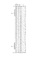
図1は、本発明の第1の実施の形態に係る半導体装置の模式的断面構造図を示す。
[First embodiment]
FIG. 1 is a schematic sectional view of a semiconductor device according to the first embodiment of the present invention.
本発明の第1の実施の形態に係る半導体装置は、図1に示すように、窒化物系化合物半導体層(3,4)上に窒化物系化合物半導体層(3,4)とショットキー接触する第1の電極7と、第1の電極7上に形成された第1の絶縁膜18と、第1の電極7から離間した窒化物系化合物半導体層(3,4)上に窒化物系化合物半導体層(3,4)と低抵抗接触する第2の電極(5,9)の第1の部分(5)と、第1の電極7と第1の絶縁膜18を介して形成され、平面的に見て、第2の電極(5,9)の第1の部分(5)側から、第1の電極7の上を跨ぐように延伸している第2の電極(5,9)の第2の部分(9)と、第2の電極(5,9)の第2の部分(9)の上に形成された第2の絶縁膜10とを有する。
As shown in FIG. 1, the semiconductor device according to the first embodiment of the present invention has a Schottky contact with a nitride compound semiconductor layer (3,4) on a nitride compound semiconductor layer (3,4). The
本発明の第1の実施の形態に係る半導体装置は、図1に示すように、第2の電極(5,9)の第2の部分(9)の厚みは第2の電極(5,9)の第1の部分(5)の厚みよりも厚く形成されていることを特徴とする。 In the semiconductor device according to the first embodiment of the present invention, as shown in FIG. 1, the thickness of the second portion (9) of the second electrode (5, 9) is the second electrode (5, 9). ) Is formed to be thicker than the thickness of the first portion (5).
また、本発明の第1の実施の形態に係る半導体装置においては、図1に示すように、第2の電極(5,9)の第2の部分(9)の厚みは第2の絶縁膜10の厚みの約5倍以上であることを特徴とする。 In the semiconductor device according to the first embodiment of the present invention, as shown in FIG. 1, the thickness of the second portion (9) of the second electrode (5, 9) is the second insulating film. It is characterized by being about 5 times the thickness of 10 or more.
また、本発明の第1の実施の形態に係る半導体装置においては、図1に示すように、第1の絶縁膜18はシリコン酸化膜で形成されていることを特徴とする。
In the semiconductor device according to the first embodiment of the present invention, as shown in FIG. 1, the first
また、本発明の第1の実施の形態に係る半導体装置においては、図1に示すように、第2の絶縁膜10はシリコン窒化膜またはポリイミド樹脂膜のいずれかまたは両方が積層されて形成されていることを特徴とする。
In the semiconductor device according to the first embodiment of the present invention, as shown in FIG. 1, the second
また、本発明の第1の実施の形態に係る半導体装置においては、図1に示すように、窒化物系化合物半導体層(3,4)はヘテロ接合を有し、ヘテロ接合面の近傍に2次元キャリアガス層が生じていることを特徴とする。 In the semiconductor device according to the first embodiment of the present invention, as shown in FIG. 1, the nitride-based compound semiconductor layers (3, 4) have a heterojunction, and 2 in the vicinity of the heterojunction surface. A dimensional carrier gas layer is formed.
図1に示すように、本発明の第1の実施の形態に係る半導体装置は、単結晶シリコン(Si)やシリコンカーバイト(SiC)、セラミックなどの基板1の上に、後述する電子走行層3と基板1との格子定数差を緩和し、電子走行層3の結晶性を良好にするための周知の緩衝層(バッファ層)2を有する。
As shown in FIG. 1, the semiconductor device according to the first embodiment of the present invention includes an electron transit layer described later on a
バッファ層2の上には第1の窒化物系化合物半導体からなる電子走行層3、第2の窒化物系化合物半導体からなる電子供給層4が順に積層されている。電子走行層3と電子供給層4との界面の電子走行層3側に2次元電子ガス層12が生じている。電子供給層4の上にはソース電極5、ドレイン電極6、ゲート電極7が設けられている。
On the
電子供給層4の上に配置されるソース電極5、およびドレイン電極6は、例えば、厚さ約25nm程度のTi層と、厚さ約500nm程度のAl層からなる積層電極構造Ti/Alをスパッタまたは真空蒸着したのちにアニールを行って形成する。
For the
また、ゲート電極7は、例えば、フォトリソグラフィー技術によって所望のパターン形状を得てから、所望のレジストパターンを形成後、厚さ約25nm程度のNi層と、厚さ約500nm程度のAl層と、厚さ約25nm程度のTi層からなる積層電極構造Ni/Al/Tiからなる積層構造をスパッタまたは真空蒸着した後にリフトオフによって形成する。
The
電流コラプス現象は、半導体装置のゲート・ドレイン間に高電圧を印加した時に、ゲート電極7からゲート・ドレイン間の表面に電子が注入されて結晶欠陥を有する窒化物系化合物半導体層(電子供給層4)の表面準位に捕獲・蓄積されて2次元電子ガス層12の電子濃度が減少し、ゲート電極7にデバイスがオン状態になる電圧を印加しても、表面準位からの電子放出が遅いために定常的なドレイン・ソース間電流Idsが減少する現象と考えられている。
The current collapse phenomenon is caused when a high voltage is applied between the gate and the drain of the semiconductor device, and electrons are injected from the
図2は、本発明の第1の実施の形態に係る半導体装置の構成において、図1に示すように、ゲート電極7上にシリコン酸化膜18を配置した場合のNi(7)/AlGaN(4)/GaN(3)近傍のバンドダイヤグラム構造図であって、バリア高さVb1を有する例の模式図を示す。また、図3は、本発明の第1の実施の形態に係る半導体装置の構成において、ゲート電極7上にシリコン酸化膜18の代りに、シリコン窒化膜を直接配置した場合のNi(7)/AlGaN(4)/GaN(3)近傍のバンドダイヤグラム構造図であって、Vb2のバリア高さを有する例の模式図を示す。図2と図3の比較から明らかなように、Vb1>Vb2であり、ゲート電極7の上にシリコン窒化膜でなく、シリコン酸化膜18を配置した図2の例の方が、ショットキー障壁が高く、ゲート電極7の漏れ電流を低減化する。また、本発明の第1の実施の形態に係る半導体装置において、上に電極が形成されていない窒化物系化合物半導体層(3,4)の露出部上に配置する絶縁膜はシリコン窒化膜に比べてシリコン酸化膜の方が好ましい。
FIG. 2 shows a structure of the semiconductor device according to the first embodiment of the present invention, in which Ni (7) / AlGaN (4) when the
シリコン窒化膜は電子供給層4に対して、電子走行層3と同様に、引っ張り応力を与えるので、電子走行層3の電子供給層4とのピエゾ分極が弱まり、電子濃度が低下して半導体装置のオン抵抗が高くなるからである。
Since the silicon nitride film gives a tensile stress to the
図1に示すように、本発明の第1の実施の形態に係る半導体装置においては、ゲート電極7を跨ぐようにシリコン酸化膜18を介してゲート電極7上を覆うようにソース電極5と電気的に接続されたソースフィールドプレート(FP)電極9がソース電極5側からドレイン電極6側へと形成されている。
As shown in FIG. 1, in the semiconductor device according to the first embodiment of the present invention, the
ソース電極5およびソースFP電極9とゲート電極7との層間絶縁膜として機能するシリコン酸化膜18の厚さは、例えば、約300〜700nm程度であり、望ましくは、例えば500nm程度である。シリコン酸化膜18を形成した場合、シリコン窒化膜(引っ張り応力、−6.14×10⁸ dyn/cm2 )と異なり、圧縮応力(4.00×10⁹ dyn/cm2 )が生じる。
The thickness of the
よって、図2に示すように、本発明の第1の実施の形態に係る半導体装置においては、ゲート電極7の上にソース電極5およびソースFP電極9との層間絶縁膜としてシリコン窒化膜を利用した場合、シリコン窒化膜の引っ張り応力がゲート電極7およびゲート電極7周囲に露出した電子供給層4に伝わり、それに伴いゲート電極7のショットキー障壁の高さが低下して、ゲート漏れ電流が増加してしまうという問題を抑制することができる。ソースFP電極9はAu、Cuを電解メッキ法またはAlをスパッタ法にて形成され、後述するポリイミド樹脂11の厚さの約1/10以上あることが望ましく、例えば3〜8μmの厚みを有する。
Therefore, as shown in FIG. 2, in the semiconductor device according to the first embodiment of the present invention, a silicon nitride film is used as an interlayer insulating film between the
シリコン酸化膜18とソースFP電極9の上面および側面を覆うようにシリコン酸化膜よりも耐湿性に優れたシリコン窒化膜10が、例えば、約400〜800nm程度、望ましくは、約500nm程度の厚さに形成されている。
A
さらにシリコン窒化膜10を覆うようにシリコン窒化膜10の上には例えば、約5〜20μm程度、望ましくは約10μm程度の厚さを有するポリイミド樹脂11が形成されている。
Further, a polyimide resin 11 having a thickness of, for example, about 5 to 20 μm, preferably about 10 μm is formed on the
図4は、本発明の第1の実施の形態に係る半導体装置において、ソースFP電極9を備える場合(D2)とソースFP電極9を備えない場合(D1)におけるドレイン・ソース間電流Ids(A/mm)とドレイン・ソース間電圧Vds(V)の関係の比較図を示す。図4から明らかなように、ソースFP電極9を備える場合(D2)の方が、ドレイン・ソース間電流Ids(A/mm)とドレイン・ソース間電圧Vds(V)の特性上、漏れ電流が抑制されている。
FIG. 4 shows the drain-source current Ids (A) when the
本発明の第1の実施の形態に係る半導体装置においては、図1に示すように、窒化物半導体層(電子供給層4)に引っ張り応力を与えてショットキー障壁の低下を引き起こすシリコン窒化膜でなく、シリコン酸化膜18が配置され、シリコン酸化膜18の上にシリコン酸化膜18よりも耐湿性に優れたシリコン窒化膜10が設けられている。
In the semiconductor device according to the first embodiment of the present invention, as shown in FIG. 1, a silicon nitride film that causes tensile stress to the nitride semiconductor layer (electron supply layer 4) to cause a reduction in the Schottky barrier is used. However, the
ただし、厚いソースFP電極9が設けられている領域においては、厚いソースFP電極9とゲート電極7の層間絶縁膜がシリコン酸化膜18となり、シリコン窒化膜10はソースFP電極9の上に形成されている。よって、シリコン窒化膜10(シリコン窒化膜10上のポリイミド樹脂11も含む)の引っ張り応力をソースFP電極9が緩和し、ゲート電極7およびその端部近傍への影響を抑制することができる。
However, in the region where the thick
また、ゲート電極7とソースFP電極9との層間絶縁膜が圧縮応力を生じさせるシリコン酸化膜18であるため、ゲート電極7およびその端部近傍に引っ張り応力が生じたとしてもそれを緩和するように働く。
In addition, since the interlayer insulating film between the
よって、図2に示すようにゲート電極7に生じる引っ張り応力によってショットキー障壁の高さが低下して、ゲート/ドレイン間あるいはゲート/ソース間の漏れ電流が1桁以上増加してしまうという問題を抑制することができる。さらに、シリコン酸化膜18の上にシリコン窒化膜10やポリイミド樹脂11が形成されているため、シリコン酸化膜18だけの場合に比べて耐湿性が高い。
Therefore, as shown in FIG. 2, the height of the Schottky barrier is lowered by the tensile stress generated in the
本発明の第1の実施の形態に係る半導体装置においては、シリコン窒化膜10またはポリイミド樹脂11のどちらかはなくても良いが、耐湿性や絶縁性をより確保するため、両方とも形成されていることが望ましい。
In the semiconductor device according to the first embodiment of the present invention, either the
さらに、本発明の第1の実施の形態に係る半導体装置において、バッファ層2は省略することもできる。
Furthermore, in the semiconductor device according to the first embodiment of the present invention, the
さらに、本発明の第1の実施の形態に係る半導体装置において、基板1が導電性基板の場合、基板1の裏面側に裏面電極を設け、ソース電極5と裏面電極を配線で電気的に接続することによって、ドレイン電極6近傍の電界集中を緩和することができる。
Furthermore, in the semiconductor device according to the first embodiment of the present invention, when the
さらに、本発明の第1の実施の形態に係る半導体装置において、電子供給層4と電子走行層3との間にAlNバリア層などによるバリア層を設けても良い。
Furthermore, in the semiconductor device according to the first embodiment of the present invention, a barrier layer such as an AlN barrier layer may be provided between the
本発明の第1の実施の形態に係る半導体装置によれば、コプラス時オン抵抗を低減化し、かつゲート漏れ電流を低減化することができる。 According to the semiconductor device of the first embodiment of the present invention, the on-resistance at the time of coplus can be reduced and the gate leakage current can be reduced.
[第2の実施形態]
図5は、本発明の第2の実施の形態に係る半導体装置の模式的断面構造図を示す。本発明の第2の実施の形態に係る半導体装置は、図5に示すように、ソース電極5にソースFP電極9を配置する構造に加えて、ゲート電極7にもゲートフィールドプレート(FP)電極17を設けて、電界集中を緩和し、電流コラプス現象を低減化し、かつゲートリーク電流を低減化する。
[Second Embodiment]
FIG. 5 is a schematic sectional view of a semiconductor device according to the second embodiment of the present invention. As shown in FIG. 5, the semiconductor device according to the second embodiment of the present invention has a gate field plate (FP) electrode in the
さらに、本発明の第2の実施の形態に係る半導体装置は、ドレイン電極6にもドレインフィールドプレート(FP)電極構造を設けて、電界集中を緩和し、電流コラプス現象を低減化し、かつゲートリーク電流を低減化することができる。例えば、図6において、さらにドレインメッキ電極60をゲート電極7もしくはゲートFP電極9側に延伸させることで、ドレイン電極6にもドレインフィールドプレート(FP)電極構造を設けることができる。
Furthermore, in the semiconductor device according to the second embodiment of the present invention, the
ゲート電極7がフィールドプレート(FP)構造となっている場合、少なくともゲート電極7上はソースFP電極9に覆われている。望ましくは、ゲートFP構造の端部よりもドレイン電極6側にまでソースFP電極9が延伸していることが望ましい。
When the
ソースFP電極9はソース電極5と一体であっても良いが、図8に示すように、互いに分離して形成され、電気的に接続された構造でもよい。
The
本発明の第2の実施の形態に係る半導体装置は、図5に示すように、窒化物系化合物半導体層(3,4)上に窒化物系化合物半導体層(3,4)とショットキー接触する第1の電極(7,17)と、第1の電極7上に形成された第1の絶縁膜(18)と、第1の電極(7,17)から離間した窒化物系化合物半導体層(3,4)上に窒化物系化合物半導体層(3,4)と低抵抗接触する第2の電極(5,50,9)の第1の部分(5)と、第1の電極(7,17)と前記第1の絶縁膜(18)を介して形成され、平面的に見て、第2の電極(5,50,9)の第1の部分(5)から、第1の電極(7,17)の上を跨ぐように延伸している第2の電極(5,50,9)の第2の部分(9)と、第2の電極(5,50,9)の第2の部分(9)の上に形成された第2の絶縁膜(10)とを有する半導体装置であって、第2の電極(5,50,9)の第2の部分の厚み(9)は第2の電極(5,50,9)の第1の部分(5)の厚みよりも厚く形成されていることを特徴とする。
As shown in FIG. 5, the semiconductor device according to the second embodiment of the present invention has a Schottky contact with the nitride compound semiconductor layer (3,4) on the nitride compound semiconductor layer (3,4). First electrode (7, 17), first insulating film (18) formed on
また、本発明の第2の実施の形態に係る半導体装置は、第2の電極(5,50,9)の第2の部分(9)の厚みは第2の絶縁膜(10)の厚みの例えば、約5倍以上であることを特徴とする。 In the semiconductor device according to the second embodiment of the present invention, the thickness of the second portion (9) of the second electrode (5, 50, 9) is equal to the thickness of the second insulating film (10). For example, it is characterized by being about 5 times or more.
また、本発明の第2の実施の形態に係る半導体装置は、図5に示すように、第1の絶縁膜はシリコン酸化膜18で形成されていることを特徴とする。
The semiconductor device according to the second embodiment of the present invention is characterized in that the first insulating film is formed of a
また、本発明の第2の実施の形態に係る半導体装置は、図5に示すように、第2の絶縁膜はシリコン窒化膜10またはポリイミド樹脂膜(11)のいずれかまたは両方が積層されて形成されていることを特徴とする。
In the semiconductor device according to the second embodiment of the present invention, as shown in FIG. 5, the second insulating film is formed by laminating one or both of the
また、本発明の第2の実施の形態に係る半導体装置は、図5に示すように、窒化物系化合物半導体層(3,4)はヘテロ接合を有し、ヘテロ接合面の近傍に2次元キャリアガス層が生じていることを特徴とする。 Further, in the semiconductor device according to the second embodiment of the present invention, as shown in FIG. 5, the nitride-based compound semiconductor layers (3,4) have a heterojunction and are two-dimensionally in the vicinity of the heterojunction plane. A carrier gas layer is formed.
また、本発明の第2の実施の形態に係る半導体装置は、図5に示すように、第1の電極(7,17)は、窒化物系化合物半導体層(3,4)とショットキー接触する第1の電極(7,17)の第1の部分(7)と、窒化物系化合物半導体層(3,4)上に第3の絶縁膜(8)を介して設けられた第1の電極(7,17)の第2の部分(17)とを有し、平面的に見て、第2の電極(5,50,9)の第2の部分(9)は第1の電極(7,17)の第1の部分(7)および第2の部分(17)を跨るように形成されていることを特徴とする。 In the semiconductor device according to the second embodiment of the present invention, as shown in FIG. 5, the first electrode (7, 17) is in Schottky contact with the nitride-based compound semiconductor layer (3,4). A first portion (7) of the first electrode (7, 17) and a first insulating layer (8) provided on the nitride-based compound semiconductor layer (3,4) via a third insulating film (8). The second part (17) of the electrode (7, 17) and the second part (9) of the second electrode (5, 50, 9) is the first electrode ( 7, 17) is formed so as to straddle the first portion (7) and the second portion (17).
図5に示すように、本発明の第2の実施の形態に係る半導体装置は、単結晶シリコン(Si)やシリコンカーバイト(SiC)、セラミックなどの基板1の上に、後述する電子走行層3と基板1との格子定数差を緩和し、電子走行層3の結晶性を良好にするための周知の緩衝層(バッファ層)2を有する。
As shown in FIG. 5, the semiconductor device according to the second embodiment of the present invention includes an electron transit layer described later on a
バッファ層2の上には第1の窒化物系化合物半導体からなる電子走行層3、第1の窒化物系化合物半導体よりも格子定数が小さい第2の窒化物系化合物半導体からなる電子供給層4が順に積層されている。電子走行層3と電子供給層4との界面の電子走行層3側に2次元電子ガス層12が生じている。電子供給層4の上にはソース電極5、ドレイン電極6、ゲート電極7が設けられている。
On the
電子供給層4の上に配置されるソース電極5、およびドレイン電極6は、例えば、厚さ約25nm程度のTi層と、厚さ約500nm程度のAl層からなる積層電極構造Ti/Alをスパッタまたは真空蒸着したのちにアニールを行って形成する。
For the
フォトリソグラフィー技術によって所望のパターン形状を得た後、ソース電極5上にはソースメッキ電極50、ドレイン電極6上にはドレインメッキ電極60が、それぞれ例えば、Auメッキによって形成される。ソースFP電極9も、ソースメッキ電極50と同時に、Auメッキによって形成可能である。
After obtaining a desired pattern shape by photolithography, a
また、ゲート電極7は、所望のレジストパターンを形成後、例えば、厚さ約25nm程度のNi層と、厚さ約500nm程度のAl層と、厚さ約25nm程度のTi層からなる積層電極構造Ni/Al/Tiからなる積層構造をスパッタまたは真空蒸着した後にリフトオフによって形成する。あるいはまた、ゲート電極7は、Ni/Auの積層構造によって形成されていてもよい。
In addition, the
電流コラプス現象は、半導体装置のゲート・ドレイン間に高電圧を印加した時に、ゲート電極7からゲート・ドレイン間の表面に電子が注入されて結晶欠陥を有する窒化物系化合物半導体層(電子供給層4)の表面準位に捕獲・蓄積されて2次元電子ガス層12の電子濃度が減少し、ゲート電極7にデバイスがオン状態となる電圧を印加しても、表面準位からの電子放出が遅いために定常的なドレイン・ソース間電流Idsが減少する現象と考えられている。
The current collapse phenomenon is caused when a high voltage is applied between the gate and the drain of the semiconductor device, and electrons are injected from the
本発明の第2の実施の形態に係る半導体装置の構成においても、本発明の第1の実施の形態に係る半導体装置と同様の効果を得ることができる。すなわち、図2と図3の比較から明らかなように、Vb1>Vb2であり、ゲート電極7の上にシリコン窒化膜でなく、シリコン酸化膜18を配置した図2の例の方が、ショットキー障壁が高く、ゲート電極7の漏れ電流を低減化する。また、本発明の第1の実施の形態に係る半導体装置において、上に電極が形成されていない窒化物系化合物半導体層(3,4)の露出部上に配置する絶縁膜はシリコン窒化膜に比べてシリコン酸化膜の方が好ましい。
Also in the configuration of the semiconductor device according to the second embodiment of the present invention, the same effect as that of the semiconductor device according to the first embodiment of the present invention can be obtained. That is, as apparent from the comparison between FIG. 2 and FIG. 3, Vb1> Vb2, and the example of FIG. 2 in which the
シリコン窒化膜は電子供給層4に対して、電子走行層3と同様に、引っ張り応力を与えるので、電子走行層3の電子供給層4とのピエゾ分極が弱まり、電子濃度が低下して半導体装置のオン抵抗が高くなるからである。
Since the silicon nitride film gives a tensile stress to the
図5に示すように、本発明の第2の実施の形態に係る半導体装置においては、ゲート電極7を跨ぐようにシリコン酸化膜18を介してゲート電極7上を覆うようにソース電極5と電気的に接続されたソースフィールドプレート(FP)電極9がソース電極5側からドレイン電極6側へと形成されている。
As shown in FIG. 5, in the semiconductor device according to the second embodiment of the present invention, the
ソース電極5およびソースFP電極9とゲート電極7との層間絶縁膜として機能するシリコン酸化膜18の厚さは、例えば、約300〜700nm程度であり、望ましくは、例えば500nm程度である。シリコン酸化膜18を形成した場合、シリコン窒化膜(引っ張り応力、−6.14×10⁸ dyn/cm2 )と異なり、圧縮応力(4.00×10⁹ dyn/cm2 )が生じる。
The thickness of the
よって、図5に示すように、本発明の第2の実施の形態に係る半導体装置においては、ゲート電極7の上にソース電極5およびソースFP電極9との層間絶縁膜としてシリコン窒化膜を利用した場合、シリコン窒化膜の引っ張り応力がゲート電極7およびゲート電極7周囲に露出した電子供給層4に伝わり、それに伴いゲート電極7のショットキー障壁の高さが低下して、ゲート漏れ電流が増加してしまうという問題を抑制することができる。
Therefore, as shown in FIG. 5, in the semiconductor device according to the second embodiment of the present invention, a silicon nitride film is used as an interlayer insulating film between the
図5に示すように、本発明の第2の実施の形態に係る半導体装置においては、ドレイン電極6を跨ぐようにシリコン酸化膜18介してドレインメッキ電極60によって、ドレインFP電極構造がドレイン電極6側にも形成されていてもよい。ドレイン電極6にもドレインフィールドプレート(FP)電極構造を設けて、電界集中を緩和し、電流コラプス現象を低減化し、かつゲートリーク電流を低減化することができる。前述の如く、例えば、図5において、さらにドレインメッキ電極60をゲート電極7もしくはゲートFP電極9側に延伸させることで、ドレイン電極6にもドレインフィールドプレート(FP)電極構造を設けることができる。
As shown in FIG. 5, in the semiconductor device according to the second embodiment of the present invention, the drain FP electrode structure is formed by the
ドレインFP電極構造によっても、ドレイン電極6近傍における電界集中が緩和され、ドレインメッキ電極60と窒化物系化合物半導体層(3,4)との間にシリコン酸化膜18を配置した構造によって、圧縮応力が加わり、2次元電子ガス層12の電子が増加し、オン抵抗を低減化することができる。
Also with the drain FP electrode structure, the electric field concentration in the vicinity of the
ゲート電極7との層間絶縁膜として機能するシリコン酸化膜18の厚さは、例えば、約300〜700nm程度であり、望ましくは、例えば500nm程度である。シリコン酸化膜18を形成した場合、シリコン窒化膜(引っ張り応力、−6.14×10⁸ dyn/cm2 )と異なり、圧縮応力(4.00×10⁹ dyn/cm2 )が生じる。
The thickness of the
よって、第1の実施の形態と同様に、本発明の第2の実施の形態に係る半導体装置においては、ショットキー障壁の高さが低下して、ゲート漏れ電流が増加してしまうという問題を抑制することができる。ソースFP電極9はAu、Cuを電解メッキ法またはAlをスパッタ法にて形成され、後述するポリイミド樹脂11の厚さの約1/10以上あることが望ましく、例えば3〜8μmの厚みを有する。
Therefore, similarly to the first embodiment, the semiconductor device according to the second embodiment of the present invention has a problem that the height of the Schottky barrier decreases and the gate leakage current increases. Can be suppressed. The
ソースFP電極9を覆うようにシリコン酸化膜よりも耐湿性に優れたシリコン窒化膜10が、例えば、約400〜800nm程度、望ましくは、約500nm程度の厚さに形成されている。
A
さらにシリコン窒化膜10を覆うようにシリコン窒化膜10の上には例えば、約5〜20μm程度、望ましくは約10μm程度の厚さを有するポリイミド樹脂11が形成されている(図示省略)。
Further, a polyimide resin 11 having a thickness of, for example, about 5 to 20 μm, preferably about 10 μm is formed on the
本発明の第2の実施の形態に係る半導体装置においても、ソースFP電極9を備える場合(D2)とソースFP電極9を備えない場合(D1)におけるドレイン・ソース間電流Ids(A/mm)とドレイン・ソース間電圧Vds(V)の関係の比較は、図4と同様に表される。ソースFP電極9を備える場合(D2)の方が、ドレイン・ソース間電流Ids(A/mm)とドレイン・ソース間電圧Vds(V)の特性上、漏れ電流が抑制されている。
Also in the semiconductor device according to the second embodiment of the present invention, the drain-source current Ids (A / mm) when the
本発明の第2の実施の形態に係る半導体装置においては、図5に示すように、窒化物半導体層(電子供給層4)に引っ張り応力を与えてショットキー障壁の低下を引き起こすシリコン窒化膜でなく、シリコン酸化膜18が配置され、シリコン酸化膜18の上にシリコン酸化膜18よりも耐湿性に優れたシリコン窒化膜10が設けられている。
In the semiconductor device according to the second embodiment of the present invention, as shown in FIG. 5, a silicon nitride film that causes tensile stress to the nitride semiconductor layer (electron supply layer 4) to cause a reduction in the Schottky barrier. However, the
ただし、厚いソースFP電極9が設けられている領域においては、厚いソースFP電極9とゲート電極7の層間絶縁膜がシリコン酸化膜18となり、シリコン窒化膜10はソースFP電極9の上に形成されている。よって、シリコン窒化膜10(シリコン窒化膜10上のポリイミド樹脂11も含む)の引っ張り応力をソースFP電極9が緩和し、ゲート電極7およびその端部近傍への影響を抑制することができる。
However, in the region where the thick
また、ゲート電極7とソースFP電極9との層間絶縁膜が圧縮応力を生じさせるシリコン酸化膜18であるため、ゲート電極7およびその端部近傍に引っ張り応力が生じたとしてもそれを緩和するように働く。
In addition, since the interlayer insulating film between the
よって、ゲート電極7に生じる引っ張り応力によってショットキー障壁の高さが低下して、ゲート・ドレイン間あるいはドレイン・ソース間あるいはゲート・ソース間の漏れ電流が1桁以上増加してしまうという問題を抑制することができる。さらに、シリコン酸化膜18の上にシリコン窒化膜10やポリイミド樹脂11が形成されているため、シリコン酸化膜18だけの場合に比べて耐湿性が高い。
Therefore, the height of the Schottky barrier is reduced due to the tensile stress generated in the
本発明の第2の実施の形態に係る半導体装置においては、シリコン窒化膜10またはポリイミド樹脂11のどちらかはなくても良いが、耐湿性や絶縁性をより確保するため、両方とも形成されていることが望ましい。
In the semiconductor device according to the second embodiment of the present invention, either the
さらに、本発明の第2の実施の形態に係る半導体装置において、バッファ層2は省略することもできる。
Furthermore, in the semiconductor device according to the second embodiment of the present invention, the
さらに、本発明の第2の実施の形態に係る半導体装置において、基板1が導電性基板の場合、基板1の裏面側に裏面電極を設け、ソース電極5と裏面電極を配線で電気的に接続することによって、ドレイン電極6近傍の電界集中を緩和することができる。
Furthermore, in the semiconductor device according to the second embodiment of the present invention, when the
さらに、本発明の第2の実施の形態に係る半導体装置において、電子供給層4と電子走行層3との間にAlNバリア層などによるバリア層を設けても良い。
Furthermore, in the semiconductor device according to the second embodiment of the present invention, a barrier layer such as an AlN barrier layer may be provided between the
本発明の第2の実施の形態に係る半導体装置の特性上、図5に示すゲート−ドレイン間距離LG-Dが一定の場合、ソースFP電極9が形成されていないシングルFP構造では、ゲートFP電極(17)−ドレイン電極(6)間距離LGF-Dに対して、コプラス時オン抵抗とパルス印加時の耐圧はトレードオフ関係にあった。一方、ゲートFP電極17の長さ(ゲートFP長)を一定とし、ソースFP電極9も形成されているダブルFP構造では、ソースFP電極9−ドレイン電極6間距離LSF-Dを短縮すると、コプラス時オン抵抗が低減した。一方、パルス印加時の耐圧はわずかに低下するだけであった。
When the gate-drain distance L GD shown in FIG. 5 is constant due to the characteristics of the semiconductor device according to the second embodiment of the present invention, in the single FP structure in which the
(変形例1)
図6は、本発明の第2の実施の形態の変形例1に係る半導体装置の模式的断面構造図を示す。本発明の第2の実施の形態の変形例1に係る半導体装置は、図6に示すように、ゲート電極7上に配置されたシリコン酸化膜18を介して、ソースFP電極9をゲート電極7上に配置した構造に特徴を有する。他の構成は基本的に図5に示す第2の実施の形態に係る半導体装置と同様であるため、説明は省略する。
(Modification 1)
FIG. 6 is a schematic cross-sectional structure diagram of a semiconductor device according to
特性上は、ソースFP電極9が、ゲートFP電極17上まで延在していないため、ゲート電極(7,17)−ドレイン電極6間の電界集中の緩和効果は、本発明の第2の実施の形態に係る半導体装置に比べて低いため、コプラス時オン抵抗の低減効果は低い。しかし、ゲート・ドレイン間あるいはドレイン・ソース間あるいはゲート・ソース間におけるゲート漏れ電流の抑制効果は本発明の第2の実施の形態に係る半導体装置と同様に高い。
Since the
一方、図6の構造において、ゲートFP電極17の長さを長くした場合の構造では、実質的に、ゲートFP電極(17)−ドレイン電極(6)間距離LGF-Dが減少するため、ゲート・ドレイン間のコプラス時オン抵抗の低減効果がある。
On the other hand, in the structure of FIG. 6, when the length of the
(変形例2)
図7は、本発明の第2の実施の形態の変形例2に係る半導体装置であって、図7(a)は模式的断面構造図、図7(b)は、図7(a)に対応する模式的平面パターン図を示す。本発明の第2の実施の形態の変形例2に係る半導体装置は、図7に示すように、ゲート電極7に対して長いゲートFP電極17を備え、ゲート電極7およびゲートFP電極17上に配置されたシリコン酸化膜18を介して、ソースFP電極9をゲート電極7およびゲートFP電極17上に配置した構造に特徴を有する。他の構成は基本的に図5に示す第2の実施の形態に係る半導体装置と同様であるため、説明は省略する。
(Modification 2)
7A and 7B show a semiconductor device according to
特性上は、ソースFP電極9が、ゲートFP電極17上まで延在しているため、ゲート電極(7,17)−ドレイン電極6間の電界集中の緩和効果は、本発明の第2の実施の形態に係る半導体装置に比べ、ゲートFP電極17が長い分だけ、さらに高い。このため、コプラス時オン抵抗の低減効果は高く、ゲート電極近傍の漏れ電流も低くなる。また、ゲート・ソース間におけるゲート漏れ電流の抑制効果は本発明の第2の実施の形態に係る半導体装置と同様に高い。
In terms of characteristics, since the
(変形例3)
図8は、本発明の第2の実施の形態の変形例3に係る半導体装置の模式的断面構造図を示す。
(Modification 3)
FIG. 8 is a schematic cross-sectional structure diagram of a semiconductor device according to
本発明の第2の実施の形態の変形例3に係る半導体装置は、図8に示すように、ゲート電極7に対して図7と同程度に長いゲートFP電極17を備え、ゲート電極7およびゲートFP電極17上に配置されたシリコン酸化膜18を介して、ソースFP電極9をソース電極5およびソースメッキ電極50ゲート電極7およびゲートFP電極17上に配置した構造に特徴を有する。しかも、ソースFP電極9は、図8の示すように、ソース電極5およびソースメッキ電極50と構造上分離して形成した点に特徴を有する。ここで、ソースFP電極9は、フローティング状態になされていてもよい。あるいは、ソースFP電極9は、一定電位が与えられていてもよい。あるいは、ソース電極5と配線その他のコンタクトを介して接続されていてもよい。
As shown in FIG. 8, the semiconductor device according to the third modification of the second embodiment of the present invention includes a
他の構成は基本的に図5に示す第2の実施の形態に係る半導体装置と同様であるため、説明は省略する。 The other configuration is basically the same as that of the semiconductor device according to the second embodiment shown in FIG.
特性上は、ソースFP電極9が、ゲートFP電極17上まで延在しているため、ゲート電極(7,17)−ドレイン電極6間の電界集中の緩和効果は、本発明の第2の実施の形態に係る半導体装置に比べ、ゲートFP電極17が長い分だけ、さらに高い。このため、コプラス時オン抵抗の低減効果は高く、ゲート電極近傍の漏れ電流も低くなる。また、ゲート・ソース間におけるゲート漏れ電流の抑制効果は本発明の第2の実施の形態に係る半導体装置と同様に高い。
In terms of characteristics, since the
ソースFP電極9をソース電極5と分離することによって、電気的にフローティング状態になされている場合には、ドレイン・ソース間のパルス耐圧を図5に示す第2の実施の形態に係る半導体装置に比べてさらに高くすることができる。パルス印加時における電圧がゲートFP電極9を介してドレイン電極6とソース電極5間で分圧されるためである。
When the
(製造方法)
図9乃至図14は、本発明の第2の実施の形態に係る半導体装置の製造方法の一工程の模式的断面構造図をそれぞれ示している。
(Production method)
FIG. 9 to FIG. 14 respectively show schematic cross-sectional structure diagrams of one step of the method for manufacturing a semiconductor device according to the second embodiment of the present invention.
本発明の第2の実施の形態に係る半導体装置の製造方法は、図9乃至図14に示すように、窒化物系化合物半導体層(3,4)の上に窒化物系化合物半導体層(3,4)と低抵抗接触する第2の電極(5,9)の第1の部分(5)およびドレイン電極(6)を形成する工程(図9)と、窒化物系化合物半導体層(3,4)の上に窒化物系化合物半導体層(3,4)とショットキー接触する第1の電極(7)を形成する工程(図10,図11)と、上面から見てほぼ全面に形成されるシリコン酸化膜(18)を形成する工程(図12)と、第2の電極(5,9)の第1の部分(5)と電気的に接続し、上面側から見て第1の電極(7)の上を跨ぐように配置され、第2の電極(5,9)の第1の部分(5)よりも厚く形成される第2の電極(5,9)の第2の部分(9)を形成する工程(図13)と、上面から見てほぼ全面に形成されるシリコン窒化膜10またはさらにポリイミド樹脂11を形成する工程(図14)とを有することを特徴とする。
As shown in FIGS. 9 to 14, the method of manufacturing a semiconductor device according to the second embodiment of the present invention has a nitride compound semiconductor layer (3) on a nitride compound semiconductor layer (3,4). , 4) forming the first portion (5) of the second electrode (5, 9) and the drain electrode (6) in low resistance contact (FIG. 9), and the nitride-based compound semiconductor layer (3, 4) forming a first electrode (7) in Schottky contact with the nitride-based compound semiconductor layer (3,4) on top of FIG. 10 and FIG. Forming a silicon oxide film (18) (FIG. 12) and the first electrode (5) electrically connected to the first part (5) of the second electrode (5, 9), as viewed from the upper surface side (7) The second electrode (5, 9) of the second electrode (5, 9) which is disposed so as to straddle over the second electrode (5, 9) and is thicker than the first portion (5) of the second electrode (5, 9). A step of forming a portion (9) (Fig. 13), characterized by a step of forming a
また、本発明の第2の実施の形態に係る半導体装置の製造方法は、図9乃至図14に示すように、窒化物系化合物半導体層(3,4)はヘテロ接合を有しており、ヘテロ界面近傍に2次元電子ガス層12を有することを特徴とする。
Further, in the method of manufacturing a semiconductor device according to the second embodiment of the present invention, as shown in FIGS. 9 to 14, the nitride-based compound semiconductor layers (3,4) have a heterojunction, A two-dimensional
図9乃至図14を参照して、本発明の第2の実施の形態に係る半導体装置の製造方法をに説明する。 A method for manufacturing a semiconductor device according to the second embodiment of the present invention will be described with reference to FIGS.
(a)まず、図9に示すように、例えばシリコンからなる基板1上にバッファ層2を介して、GaAlN層などからなる電子走行層3、GaN層などからなる電子供給層4を形成後、ソース電極5およびドレイン電極6をパターニングにより形成する。
(A) First, as shown in FIG. 9, after an
(b)次に、図10に示すように、半導体ウェハ全面にシリコン酸化膜8を形成し、パターニングによりゲート電極の形成予定部分に対して窓開けする。
(B) Next, as shown in FIG. 10, a
(c)次に、図11に示すように、ゲート電極7をパターニングにより形成する。
(C) Next, as shown in FIG. 11, the
(d)次に、図12に示すように、半導体ウェハ全面にシリコン酸化膜18を形成し、パターニングによりソース電極5、およびドレイン電極6に対して窓開けする。
(D) Next, as shown in FIG. 12, a
(e)次に、図13に示すように、ソース電極5およびドレイン電極6上にそれぞれソースメッキ電極50およびドレインメッキ電極60を形成し、同時にゲート電極7およびゲートFP電極を覆うように、シリコン酸化膜18を介して、ソースFP電極9を形成する。図13に示される構造は、図7に示す、本発明の第2の実施の形態の変形例2に係る半導体装置において、ゲートFP電極17を短く形成した構造に対応している。
(E) Next, as shown in FIG. 13, the
(f)次に、図14に示すように、半導体ウェハ全面にシリコン窒化膜10を形成し、さらにポリイミド樹脂11を形成する。
(F) Next, as shown in FIG. 14, a
(カスコード回路)
図15は、本発明の実施の形態に係る半導体装置である高耐圧GaNFETを低耐圧SiMOSFETとカスコード接続した回路構成図を示す。
(Cascode circuit)
FIG. 15 shows a circuit configuration diagram in which a high breakdown voltage GaNFET which is a semiconductor device according to an embodiment of the present invention is cascode-connected to a low breakdown voltage SiMOSFET.
(特性例)
図16は、図15に示す高耐圧GaNFETを低耐圧SiMOSFETとカスコード接続した回路構成において、ドレイン・ソース間電流Ids(A)とゲート・ソース間電圧Vgs(V)の伝達特性の比較図を示す。高耐圧GaNFET単体では、ノーマリオン特性であっても、低耐圧SiMOSFETとカスコード接続することによって、ノーマリオフ特性を得ることができる。
(Example of characteristics)
FIG. 16 is a comparison diagram of transfer characteristics of the drain-source current Ids (A) and the gate-source voltage Vgs (V) in the circuit configuration in which the high breakdown voltage GaNFET shown in FIG. 15 is cascode-connected to the low breakdown voltage SiMOSFET. . A single high-voltage GaNFET can provide a normally-off characteristic by cascode connection with a low-voltage SiMOSFET even if it has a normally-on characteristic.
図17は、入力容量Ciss(pF)のドレイン・ソース間電圧Vds(V)特性の比較図を示す。GaNFET単体の場合に比べれば入力容量Ciss(pF)は大きくなるが、GaNFETをSiMOSFETとカスコード接続することによって、単体のSiMOSFETの場合よりも入力容量Ciss(pF)を低減化することができる。このため、高速スイッチング性能を得ることができる。 FIG. 17 shows a comparison diagram of the drain-source voltage Vds (V) characteristics of the input capacitance Ciss (pF). Although the input capacitance Ciss (pF) is larger than that of a single GaNFET, the input capacitance Ciss (pF) can be reduced by cascode-connecting the GaNFET to the SiMOSFET as compared to the case of a single SiMOSFET. For this reason, high-speed switching performance can be obtained.
図18は、本発明の実施の形態に係る半導体装置である高耐圧GaNFETを低耐圧SiMOSFETとカスコード接続した回路をPFC(Power Factor Correction)回路に適用した場合のスイッチング波形例であって、(a)Vds=440(V)、Ids=6.2(A)の連続スイッチング波形、(b)ターン・オフ波形の拡大図、(c)ターン・オン波形の拡大図をそれぞれ示している。 FIG. 18 is an example of switching waveforms when a circuit in which a high breakdown voltage GaNFET, which is a semiconductor device according to an embodiment of the present invention, is cascode-connected to a low breakdown voltage SiMOSFET is applied to a PFC (Power Factor Correction) circuit. ) Vds = 440 (V), Ids = 6.2 (A) continuous switching waveform, (b) Enlarged view of turn-off waveform, (c) Enlarged view of turn-on waveform.
SiMOSFET単体のみの場合に比較して、Vdsの立上り波形におけるターン・オフ時間は約40%改善されて高速化された。また、Idsの立上り波形におけるピーク電流値は、SiMOSFET単体のみの場合に比較して、約30%低減され、低ノイズ化された。PFC回路搭載時の電力変換効率は、SiMOSFET単体のみの場合に比較して上昇し、かつ低ノイズであることからノイズ抑制回路の削減、高周波化、小型化を実現することができる。 Compared with the case of using only the SiMOSFET alone, the turn-off time in the rising waveform of Vds is improved by about 40% and speeded up. In addition, the peak current value in the rising waveform of Ids was reduced by about 30% compared with the case of only the SiMOSFET alone, and the noise was reduced. The power conversion efficiency when the PFC circuit is mounted increases as compared with the case of using only the SiMOSFET alone and is low in noise, so that it is possible to reduce the noise suppression circuit, increase the frequency, and reduce the size.
本発明の第2の実施の形態に係る半導体装置によれば、コプラス時オン抵抗を低減化し、かつゲート漏れ電流を低減化することができる。 According to the semiconductor device of the second embodiment of the present invention, the on-resistance at the time of coplus can be reduced and the gate leakage current can be reduced.
[その他の実施の形態]
上記のように、本発明は第1乃至第2の実施の形態によって記載したが、この開示の一部をなす論述および図面はこの発明を限定するものでないと理解すべきである。この開示から当業者には様々な代替実施の形態、実施例および運用技術が明らかとなろう。
[Other embodiments]
As described above, the present invention has been described according to the first to second embodiments. However, it should be understood that the description and drawings constituting a part of this disclosure do not limit the present invention. From this disclosure, various alternative embodiments, examples and operational techniques will be apparent to those skilled in the art.
例えば、本発明の実施の形態に係る半導体装置は、第1の実施の形態で示す高電子移動度トランジスタ(HEMT:High Electron Mobility Transistor)に限定されず、複数の素子が形成された複合半導体装置であってもよい。 For example, the semiconductor device according to the embodiment of the present invention is not limited to the high electron mobility transistor (HEMT) shown in the first embodiment, and is a composite semiconductor device in which a plurality of elements are formed. It may be.
また、デバイス形成層の構造を変更することにより、本発明の実施の形態に係る半導体基板は、発光ダイオード、半導体レーザーなどの発光素子、金属-半導体電界効果トランジスタ(MESFET:Metal Semiconductor Field Effect Transistor)、金属-酸化物-半導体電界効果トランジスタ(MOSFET:Metal Oxide Semiconductor Field Effect Transistor)、金属-絶縁物-半導体電界効果トランジスタ(MISFET:Metal Insulator Semiconductor Field Effect Transistor)、ヘテロ接合バイポーラトランジスタ(HBT:Hetero-junction Bipolar Transistor)などにも適用可能である。 Further, by changing the structure of the device formation layer, the semiconductor substrate according to the embodiment of the present invention can be obtained by using a light emitting element such as a light emitting diode or a semiconductor laser, a metal semiconductor field effect transistor (MESFET). Metal-Oxide Semiconductor Field Effect Transistor (MOSFET), Metal-Insulator-Semiconductor Field Effect Transistor (MISFET), Heterojunction Bipolar Transistor (HBT) Junction Bipolar Transistor) is also applicable.
このように、本発明はここでは記載していない様々な実施の形態などを含むことは勿論である。したがって、本発明の技術的範囲は上記の説明から妥当な特許請求の範囲に係る発明特定事項によってのみ定められるものである。 As described above, the present invention naturally includes various embodiments that are not described herein. Therefore, the technical scope of the present invention is defined only by the invention specifying matters according to the scope of claims reasonable from the above description.
1…基板
2…バッファ層
3…電子走行層
4…電子供給層
5…ソース電極
6…ドレイン電極
7…ゲート電極
8,18…シリコン酸化膜
9…ソースフィールドプレート(ソースFP)電極
10…シリコン窒化膜
11…ポリイミド樹脂
12…2次元電子ガス(2DEG)層
17…ゲートフィールドプレート(ゲートFP)電極
50…ソースメッキ電極
60…ドレインメッキ電極
DESCRIPTION OF
Claims (11)
前記第1の電極上に形成され、前記電子供給層に圧縮応力を与える第1の絶縁膜と、
前記第1の電極から離間した前記窒化物系化合物半導体層上に前記窒化物系化合物半導体層と低抵抗接触する第2の電極の第1の部分と、
前記第1の電極と前記第1の絶縁膜を介して形成され、前記第2の電極の第1の部分と電気的に接続し、平面的に見て、前記第1の電極の上を跨ぐように延伸している第2の電極の第2の部分と、
前記第2の電極の第2の部分の上に形成され、前記電子供給層に引っ張り応力を与える第2の絶縁膜と
を有する半導体装置であって、
前記第2の電極の第2の部分の厚みは、前記第2の絶縁膜による前記引っ張り応力を緩和するために前記第2の電極の第1の部分の厚みよりも厚く形成されていることを特徴とする半導体装置。 A first electrode in Schottky contact with the nitride compound semiconductor layer on a nitride compound semiconductor layer having an electron transit layer and an electron supply layer disposed on the electron transit layer ;
A first insulating film formed on the first electrode and applying compressive stress to the electron supply layer ;
A first portion of a second electrode in low resistance contact with the nitride compound semiconductor layer on the nitride compound semiconductor layer spaced from the first electrode;
Formed via the first electrode and the first insulating film, electrically connected to the first portion of the second electrode and straddling the first electrode when viewed in plan A second portion of the second electrode extending in such a way that
A second insulating film formed on a second portion of the second electrode and applying a tensile stress to the electron supply layer ,
The thickness of the second portion of the second electrode is made thicker than the thickness of the first portion of the second electrode in order to relieve the tensile stress due to the second insulating film. A featured semiconductor device.
前記第2の電極の第2の部分の厚みは第2の絶縁膜の厚みの5倍以上であることを特徴とする半導体装置。 The semiconductor device according to claim 1,
The thickness of the 2nd part of the said 2nd electrode is 5 times or more of the thickness of a 2nd insulating film, The semiconductor device characterized by the above-mentioned.
前記ゲート電極上に形成され、前記電子供給層に圧縮応力を与える第1の絶縁膜と、
前記ゲート電極から離間した前記窒化物系化合物半導体層上に前記窒化物系化合物半導体層と低抵抗接触するソース電極の第1の部分と、
前記ゲート電極と前記第1の絶縁膜を介して形成され、前記ソース電極の第1の部分と電気的に接続し、平面的に見て、前記ゲート電極の上を跨ぐように延伸している前記ソース電極の第2の部分と、
前記ソース電極の第2の部分の上に形成され、前記電子供給層に引っ張り応力を与える第2の絶縁膜と
を有する半導体装置であって、
前記ソース電極の第2の部分の厚みは、前記第2の絶縁膜による前記引っ張り応力を緩和するために前記ソース電極の第1の部分の厚みよりも厚く形成されていることを特徴とする半導体装置。 A gate electrode having an MIS structure on a nitride compound semiconductor layer having an electron transit layer and an electron supply layer disposed on the electron transit layer, and the nitride compound semiconductor layer and a Schottky contact or an insulating film; ,
A first insulating film formed on the gate electrode and applying compressive stress to the electron supply layer ;
A first portion of a source electrode in low resistance contact with the nitride compound semiconductor layer on the nitride compound semiconductor layer spaced from the gate electrode;
Formed through the gate electrode and the first insulating film, electrically connected to the first portion of the source electrode, and extended across the gate electrode in plan view. A second portion of the source electrode;
A second insulating film formed on the second portion of the source electrode and applying a tensile stress to the electron supply layer ,
The thickness of the second portion of the source electrode is formed to be thicker than the thickness of the first portion of the source electrode in order to relieve the tensile stress caused by the second insulating film. apparatus.
前記ソース電極の第2の部分の厚みは第2の絶縁膜の厚みの5倍以上であることを特徴とする半導体装置。 The semiconductor device according to claim 3.
The semiconductor device according to claim 1, wherein the thickness of the second portion of the source electrode is at least five times the thickness of the second insulating film.
前記第1の絶縁膜はシリコン酸化膜で形成されていることを特徴とする半導体装置。 The semiconductor device according to claim 1,
The semiconductor device, wherein the first insulating film is formed of a silicon oxide film.
前記第2の絶縁膜はシリコン窒化膜またはポリイミド樹脂膜のいずれかまたは両方が積層されて形成されていることを特徴とする半導体装置。 The semiconductor device according to claim 1,
The semiconductor device, wherein the second insulating film is formed by laminating one or both of a silicon nitride film and a polyimide resin film.
前記窒化物系化合物半導体層はヘテロ接合を有し、ヘテロ接合面の近傍に2次元キャリアガス層が生じていることを特徴とする半導体装置。 The semiconductor device according to claim 1,
The nitride compound semiconductor layer has a heterojunction, and a two-dimensional carrier gas layer is generated in the vicinity of the heterojunction surface.
前記ゲート電極は、
前記窒化物系化合物半導体層とショットキー接触もしくは絶縁膜を介してMIS構造を備える前記ゲート電極の第1の部分と、
前記窒化物系化合物半導体層上に第3の絶縁膜を介して設けられた前記ゲート電極の第2の部分と
を有し、
平面的に見て、前記第2の電極の第2の部分は前記第1の電極の第1の部分および第2の部分を跨るように形成されていることを特徴とする半導体装置。 The semiconductor device according to claim 3,
The gate electrode is
A first portion of the gate electrode having a MIS structure via a Schottky contact or an insulating film with the nitride-based compound semiconductor layer;
A second portion of the gate electrode provided on the nitride-based compound semiconductor layer via a third insulating film,
The semiconductor device, wherein the second portion of the second electrode is formed so as to straddle the first portion and the second portion of the first electrode when viewed in a plan view.
窒化物系化合物半導体層の上に前記窒化物系化合物半導体層とショットキー接触する第1の電極を形成する工程と、
前記第1の電極上に、前記電子供給層に圧縮応力を与える第1の絶縁膜を形成する工程と、
前記第2の電極の第1の部分と電気的に接続し、上面側から見て前記第1の電極の上を跨ぐように前記第1の電極と前記第1の絶縁膜を介して配置され、前記第2の電極の第1の部分よりも厚く形成される前記第2の電極の第2の部分を形成する工程と、
前記第2の電極の第2の部分上に、前記電子供給層に引っ張り応力を与える第2の絶縁膜を形成する工程と を有し、前記第2の絶縁膜による前記引っ張り応力を緩和するために前記第2の部分の厚みを前記第1の部分の厚みよりも厚く形成することを特徴とする半導体装置の製造方法。 Forming a first portion of a second electrode in low resistance contact with the nitride compound semiconductor layer on a nitride compound semiconductor layer having an electron transit layer and an electron supply layer disposed on the electron transit layer And a process of
Forming a first electrode in Schottky contact with the nitride compound semiconductor layer on the nitride compound semiconductor layer;
Forming a first insulating film on the first electrode that applies compressive stress to the electron supply layer ;
It is electrically connected to the first portion of the second electrode, and is disposed via the first electrode and the first insulating film so as to straddle over the first electrode when viewed from the upper surface side. Forming a second portion of the second electrode formed thicker than the first portion of the second electrode;
On a second portion of said second electrode, and organic and forming a second insulating film provided with tensile stress on the electron supply layer, in order to relieve the tensile stress due to the second insulating film And forming a thickness of the second portion larger than a thickness of the first portion .
前記窒化物系化合物半導体層はヘテロ接合を有しており、ヘテロ界面近傍に2次元電子ガス層を有することを特徴とする半導体装置の製造方法。 In the manufacturing method of the semiconductor device according to claim 9,
The nitride compound semiconductor layer has a heterojunction, and has a two-dimensional electron gas layer in the vicinity of the heterointerface.
前記第1の絶縁膜はシリコン酸化膜で形成され、前記第2の絶縁膜は、シリコン窒化膜で形成されることを特徴とする半導体装置の製造方法。 In the manufacturing method of the semiconductor device according to claim 9 or 10,
The method of manufacturing a semiconductor device, wherein the first insulating film is formed of a silicon oxide film, and the second insulating film is formed of a silicon nitride film.
Priority Applications (1)
| Application Number | Priority Date | Filing Date | Title |
|---|---|---|---|
| JP2007079229A JP5386785B2 (en) | 2007-03-26 | 2007-03-26 | Semiconductor device and manufacturing method thereof |
Applications Claiming Priority (1)
| Application Number | Priority Date | Filing Date | Title |
|---|---|---|---|
| JP2007079229A JP5386785B2 (en) | 2007-03-26 | 2007-03-26 | Semiconductor device and manufacturing method thereof |
Publications (2)
| Publication Number | Publication Date |
|---|---|
| JP2008243943A JP2008243943A (en) | 2008-10-09 |
| JP5386785B2 true JP5386785B2 (en) | 2014-01-15 |
Family
ID=39914958
Family Applications (1)
| Application Number | Title | Priority Date | Filing Date |
|---|---|---|---|
| JP2007079229A Active JP5386785B2 (en) | 2007-03-26 | 2007-03-26 | Semiconductor device and manufacturing method thereof |
Country Status (1)
| Country | Link |
|---|---|
| JP (1) | JP5386785B2 (en) |
Cited By (1)
| Publication number | Priority date | Publication date | Assignee | Title |
|---|---|---|---|---|
| US9419119B2 (en) | 2014-09-16 | 2016-08-16 | Kabushiki Kaisha Toshiba | Semiconductor device and manufacturing method thereof |
Families Citing this family (24)
| Publication number | Priority date | Publication date | Assignee | Title |
|---|---|---|---|---|
| JP5487613B2 (en) * | 2008-12-19 | 2014-05-07 | 富士通株式会社 | Compound semiconductor device and manufacturing method thereof |
| JP2010205440A (en) * | 2009-02-27 | 2010-09-16 | Toshiba Lighting & Technology Corp | Lighting system |
| JP2011029386A (en) * | 2009-07-24 | 2011-02-10 | Sharp Corp | Semiconductor device and electronic apparatus |
| US20120241820A1 (en) * | 2011-03-21 | 2012-09-27 | International Rectifier Corporation | III-Nitride Transistor with Passive Oscillation Prevention |
| US9236376B2 (en) | 2011-03-21 | 2016-01-12 | Infineon Technologies Americas Corp. | Power semiconductor device with oscillation prevention |
| US9859882B2 (en) | 2011-03-21 | 2018-01-02 | Infineon Technologies Americas Corp. | High voltage composite semiconductor device with protection for a low voltage device |
| US8766375B2 (en) | 2011-03-21 | 2014-07-01 | International Rectifier Corporation | Composite semiconductor device with active oscillation prevention |
| US9362905B2 (en) | 2011-03-21 | 2016-06-07 | Infineon Technologies Americas Corp. | Composite semiconductor device with turn-on prevention control |
| JP2013038239A (en) * | 2011-08-09 | 2013-02-21 | Sanken Electric Co Ltd | Nitride semiconductor device |
| JP2013062494A (en) * | 2011-08-24 | 2013-04-04 | Sanken Electric Co Ltd | Nitride semiconductor device |
| JP5653326B2 (en) | 2011-09-12 | 2015-01-14 | 株式会社東芝 | Nitride semiconductor device |
| JP2014029991A (en) * | 2012-06-29 | 2014-02-13 | Sharp Corp | Nitride semiconductor device electrode structure and nitride semiconductor field effect transistor |
| JP6178065B2 (en) * | 2012-10-09 | 2017-08-09 | 株式会社東芝 | Semiconductor device |
| US8916427B2 (en) * | 2013-05-03 | 2014-12-23 | Texas Instruments Incorporated | FET dielectric reliability enhancement |
| JP2014229823A (en) * | 2013-05-24 | 2014-12-08 | 古河電気工業株式会社 | Semiconductor device and semiconductor module |
| JP6252122B2 (en) * | 2013-11-13 | 2017-12-27 | 富士通株式会社 | Semiconductor device and manufacturing method of semiconductor device |
| JP2015220430A (en) * | 2014-05-21 | 2015-12-07 | シャープ株式会社 | Field effect transistor |
| JP6575224B2 (en) * | 2015-08-21 | 2019-09-18 | 株式会社デンソー | Semiconductor device |
| WO2017098603A1 (en) * | 2015-12-09 | 2017-06-15 | 三菱電機株式会社 | Nitride semiconductor device |
| JP6195041B1 (en) | 2016-10-24 | 2017-09-13 | 三菱電機株式会社 | Method for manufacturing compound semiconductor device |
| US10957770B2 (en) | 2016-10-24 | 2021-03-23 | Mitsubishi Electric Corporation | Method for manufacturing compound semiconductor device |
| WO2018078894A1 (en) * | 2016-10-24 | 2018-05-03 | 三菱電機株式会社 | Compound semiconductor device |
| JP7131155B2 (en) * | 2018-07-18 | 2022-09-06 | サンケン電気株式会社 | semiconductor equipment |
| JP7487094B2 (en) | 2020-12-23 | 2024-05-20 | 株式会社 日立パワーデバイス | Semiconductor Device |
Family Cites Families (3)
| Publication number | Priority date | Publication date | Assignee | Title |
|---|---|---|---|---|
| US7573078B2 (en) * | 2004-05-11 | 2009-08-11 | Cree, Inc. | Wide bandgap transistors with multiple field plates |
| JP4902131B2 (en) * | 2005-03-31 | 2012-03-21 | 住友電工デバイス・イノベーション株式会社 | Semiconductor device and manufacturing method thereof |
| JP4897948B2 (en) * | 2005-09-02 | 2012-03-14 | 古河電気工業株式会社 | Semiconductor element |
-
2007
- 2007-03-26 JP JP2007079229A patent/JP5386785B2/en active Active
Cited By (1)
| Publication number | Priority date | Publication date | Assignee | Title |
|---|---|---|---|---|
| US9419119B2 (en) | 2014-09-16 | 2016-08-16 | Kabushiki Kaisha Toshiba | Semiconductor device and manufacturing method thereof |
Also Published As
| Publication number | Publication date |
|---|---|
| JP2008243943A (en) | 2008-10-09 |
Similar Documents
| Publication | Publication Date | Title |
|---|---|---|
| JP5386785B2 (en) | Semiconductor device and manufacturing method thereof | |
| US8928039B2 (en) | Semiconductor device including heterojunction field effect transistor and Schottky barrier diode | |
| US7498617B2 (en) | III-nitride integrated schottky and power device | |
| JP5776217B2 (en) | Compound semiconductor device | |
| JP6230456B2 (en) | Semiconductor device | |
| JP5789967B2 (en) | Semiconductor device, manufacturing method thereof, and power supply device | |
| US8823061B2 (en) | Semiconductor device | |
| CN101299437A (en) | Field effect transistor having field plate electrodes | |
| JP5712516B2 (en) | Semiconductor device | |
| JPWO2006132418A1 (en) | Field effect transistor | |
| JP6614116B2 (en) | Semiconductor device | |
| JP2007273640A (en) | Semiconductor device | |
| CN110212028B (en) | Lateral diffusion eGaN HEMT device integrating reverse diode and embedded drain electrode field plate | |
| JP2009253126A (en) | Semiconductor device | |
| WO2010047016A1 (en) | Bidirectional switch | |
| US20130009676A1 (en) | Bidirectional switching device and bidirectional switching circuit using the same | |
| CN102222689A (en) | Semiconductor device | |
| TW202101717A (en) | Integrated design for iii-nitride devices | |
| KR20140012507A (en) | High electron mobility transistor and method of manufacturing the same | |
| US9324851B2 (en) | DC/DC converter circuit of semiconductor device having a first transistor of a normally-off type and a second transistor of a normally-on type | |
| CN104704616A (en) | Field-effect transistor | |
| US20220392887A1 (en) | Semiconductor device | |
| JP2008244001A (en) | Nitride semiconductor device | |
| WO2007081807A2 (en) | Iii-nitride power semiconductor with a field relaxation feature | |
| JP2013062494A (en) | Nitride semiconductor device |
Legal Events
| Date | Code | Title | Description |
|---|---|---|---|
| A621 | Written request for application examination |
Free format text: JAPANESE INTERMEDIATE CODE: A621 Effective date: 20100301 |
|
| A977 | Report on retrieval |
Free format text: JAPANESE INTERMEDIATE CODE: A971007 Effective date: 20121022 |
|
| A131 | Notification of reasons for refusal |
Free format text: JAPANESE INTERMEDIATE CODE: A131 Effective date: 20121106 |
|
| A521 | Request for written amendment filed |
Free format text: JAPANESE INTERMEDIATE CODE: A523 Effective date: 20121228 |
|
| A131 | Notification of reasons for refusal |
Free format text: JAPANESE INTERMEDIATE CODE: A131 Effective date: 20130423 |
|
| A521 | Request for written amendment filed |
Free format text: JAPANESE INTERMEDIATE CODE: A523 Effective date: 20130617 |
|
| TRDD | Decision of grant or rejection written | ||
| A01 | Written decision to grant a patent or to grant a registration (utility model) |
Free format text: JAPANESE INTERMEDIATE CODE: A01 Effective date: 20130910 |
|
| A61 | First payment of annual fees (during grant procedure) |
Free format text: JAPANESE INTERMEDIATE CODE: A61 Effective date: 20130923 |
|
| R150 | Certificate of patent or registration of utility model |
Ref document number: 5386785 Country of ref document: JP Free format text: JAPANESE INTERMEDIATE CODE: R150 Free format text: JAPANESE INTERMEDIATE CODE: R150 |
|
| R250 | Receipt of annual fees |
Free format text: JAPANESE INTERMEDIATE CODE: R250 |
|
| R250 | Receipt of annual fees |
Free format text: JAPANESE INTERMEDIATE CODE: R250 |
|
| R250 | Receipt of annual fees |
Free format text: JAPANESE INTERMEDIATE CODE: R250 |
|
| R250 | Receipt of annual fees |
Free format text: JAPANESE INTERMEDIATE CODE: R250 |
|
| R250 | Receipt of annual fees |
Free format text: JAPANESE INTERMEDIATE CODE: R250 |
|
| R250 | Receipt of annual fees |
Free format text: JAPANESE INTERMEDIATE CODE: R250 |
|
| R250 | Receipt of annual fees |
Free format text: JAPANESE INTERMEDIATE CODE: R250 |
|
| R250 | Receipt of annual fees |
Free format text: JAPANESE INTERMEDIATE CODE: R250 |
|
| R250 | Receipt of annual fees |
Free format text: JAPANESE INTERMEDIATE CODE: R250 |