JP5380791B2 - Optical element, labeled article, optical kit, and discrimination method - Google Patents
Optical element, labeled article, optical kit, and discrimination method Download PDFInfo
- Publication number
- JP5380791B2 JP5380791B2 JP2007154555A JP2007154555A JP5380791B2 JP 5380791 B2 JP5380791 B2 JP 5380791B2 JP 2007154555 A JP2007154555 A JP 2007154555A JP 2007154555 A JP2007154555 A JP 2007154555A JP 5380791 B2 JP5380791 B2 JP 5380791B2
- Authority
- JP
- Japan
- Prior art keywords
- optical element
- liquid crystal
- observed
- layer
- recess forming
- Prior art date
- Legal status (The legal status is an assumption and is not a legal conclusion. Google has not performed a legal analysis and makes no representation as to the accuracy of the status listed.)
- Expired - Fee Related
Links
Images


Landscapes
- Credit Cards Or The Like (AREA)
- Holo Graphy (AREA)
Description
本発明は、例えば、偽造防止効果、装飾効果及び/又は美的効果を提供する表示技術に関する。 The present invention relates to a display technology that provides, for example, an anti-counterfeit effect, a decorative effect, and / or an aesthetic effect.
偽造防止には、潜像を利用することがある。潜像は、例えば、万線モアレ又は凹版印刷を利用して形成することができる。 A latent image may be used to prevent forgery. The latent image can be formed using, for example, line moire or intaglio printing.
万線モアレを利用した潜像は、潜像とすべき像と、高密度に配列した多数の線とを重ねることにより得られる。この像は、肉眼で観察した場合には多数の線が識別を困難とし、それら線を隠すことにより識別が容易になる。 A latent image using line moire is obtained by superimposing an image to be a latent image and a large number of lines arranged at high density. When this image is observed with the naked eye, many lines make it difficult to identify, and hiding these lines facilitates identification.
凹版印刷を利用した潜像は、インキ層に凹パターン及び/又は凸パターンを設けることにより得られる。凹パターン及び/又は凸パターンが形成している像は、正面から観察した場合には識別が困難であり、斜めから観察することにより可視化する。 A latent image using intaglio printing is obtained by providing a concave pattern and / or a convex pattern in the ink layer. The image formed by the concave pattern and / or the convex pattern is difficult to identify when viewed from the front, and is visualized by observing from an oblique direction.
万線モアレ又は凹版印刷を利用した偽造防止技術は、真偽判定が比較的容易である。しかしながら、これらの方法で形成した像は、肉眼で観察した場合に識別が不可能な訳ではない。そのため、これら潜像は、それ自体の存在を悟られ易い。 Forgery prevention technology using line moiré or intaglio printing is relatively easy to determine authenticity. However, images formed by these methods are not necessarily indistinguishable when observed with the naked eye. Therefore, these latent images are easy to realize their existence.
潜像は、蛍光インキ及び赤外線吸収インキなどの特殊インキを使用して形成することもできる。蛍光インキは、紫外線を照射することにより発光するインキであって、これを用いて形成した潜像は、紫外線照射により可視化する。赤外線吸収インキは、赤外線吸収率が高いインキであって、これを用いて形成した潜像は、例えば、赤外線カメラで観察することにより可視化する。 The latent image can also be formed using special inks such as fluorescent ink and infrared absorbing ink. The fluorescent ink is an ink that emits light when irradiated with ultraviolet rays, and a latent image formed using the fluorescent ink is visualized when irradiated with ultraviolet rays. The infrared absorbing ink is an ink having a high infrared absorption rate, and a latent image formed using the infrared absorbing ink is visualized by observing with an infrared camera, for example.
特殊インキを使用して形成した潜像は、それ自体の存在を悟られ難い。しかしながら、その可視化には、紫外線ランプ又は赤外線カメラなどの装置が必要である。 Latent images formed using special inks are difficult to realize. However, the visualization requires a device such as an ultraviolet lamp or an infrared camera.
潜像は、液晶材料を使用して形成することもできる。例えば、光反射性を有する基材上に、高分子液晶材料などの固化した液晶材料からなる薄膜パターンを形成する。液晶分子のメソゲン基は、例えば、薄膜パターンの下地にラビング処理又は光配向処理などの配向処理を施しておくことにより、略一方向に配向させる。 The latent image can also be formed using a liquid crystal material. For example, a thin film pattern made of a solidified liquid crystal material such as a polymer liquid crystal material is formed on a substrate having light reflectivity. The mesogenic groups of the liquid crystal molecules are aligned in approximately one direction by, for example, performing an alignment process such as a rubbing process or a photo-alignment process on the base of the thin film pattern.
この薄膜パターンは、肉眼で観察した場合には、光学的に等方性の層と同様に見える。それゆえ、この薄膜パターンで潜像を構成することができる。そして、この薄膜パターンは位相差層として機能するので、偏光子を介して観察した場合には、その遅相軸と偏光子の光透過軸とが為す角度に応じた明るさの変化を生じる。すなわち、この薄膜パターンが形成している潜像は、偏光子を介して観察することにより可視化する。 This thin film pattern looks like an optically isotropic layer when viewed with the naked eye. Therefore, a latent image can be formed with this thin film pattern. Since this thin film pattern functions as a retardation layer, when observed through a polarizer, a change in brightness according to the angle formed by the slow axis and the light transmission axis of the polarizer occurs. That is, the latent image formed by the thin film pattern is visualized by observing through a polarizer.
液晶材料を使用して形成した潜像は、それ自体の存在が悟られ難い。加えて、この潜像は、偏光フィルムなどの偏光子で可視化することができ、大きな装置は不要である。そのため、液晶材料を使用した偽造防止技術は、高い関心を集めている。 A latent image formed using a liquid crystal material is difficult to realize. In addition, the latent image can be visualized with a polarizer such as a polarizing film, and a large apparatus is not required. For this reason, anti-counterfeiting technology using a liquid crystal material has attracted high interest.
例えば、特許文献1には、OVD(optically variable device)層と潜像形成層とを積層することが記載されている。潜像形成層は、例えば、高分子液晶材料からなる。OVD層は、例えば、ホログラムである。
For example,
この積層体を肉眼で観察した場合には、ホログラムの視覚効果、すなわち、虹色及び観察角度に応じた色変化を確認することができる。そして、潜像形成層が形成している潜像は、偏光子を介して観察することにより可視化する。このように、液晶材料とホログラムとを組み合わせると、多様に変化する像を形成することができる。したがって、液晶材料のみを使用した場合と比較して、より高い偽造防止効果を達成できる。 When this laminate is observed with the naked eye, the visual effect of the hologram, that is, the rainbow color and the color change corresponding to the observation angle can be confirmed. The latent image formed by the latent image forming layer is visualized by observing through a polarizer. As described above, when the liquid crystal material and the hologram are combined, an image that changes variously can be formed. Therefore, a higher forgery prevention effect can be achieved as compared with the case where only the liquid crystal material is used.
しかしながら、偽造技術の進歩は著しい。それゆえ、偽造防止技術には更なる進歩が望まれている。
本発明の目的は、固化した液晶材料を含んだ光学素子が表示する像の観察条件に応じた変化の多様性を高めることにある。 An object of the present invention is to increase the variety of changes according to viewing conditions of an image displayed by an optical element including a solidified liquid crystal material.
本発明の第1側面によると、光透過性の凹部形成層であって、その一方の主面に、それぞれ長さ方向が揃っていると共に前記長さ方向と交差する方向に隣り合った複数の溝が各々に設けられた1つ又は複数の凹部形成領域を含んだ凹部形成層と、前記凹部形成層の前記一方の主面に支持されると共に固化された液晶材料からなる液晶層と、前記凹部形成層の他方の主面と向き合った鏡面反射層とを具備し、前記複数の凹部形成領域において、一の凹部形成領域の複数の溝は、長さ方向、深さ及び/又は幅が、他の凹部形成領域の複数の溝と異なり、前記1つ又は複数の凹部形成領域の少なくとも1つには、前記複数の溝として、幅方向に隣り合う溝間の距離が不均一であり、一方向性拡散パターンを形成しているもののみが設けられていることを特徴とする光学素子が提供される。 According to a first aspect of the present invention, a plurality a light transmissive recess forming layer, the main surface of the hand, which are neighboring in the direction crossing the longitudinal direction with are What lengthwise direction Assortment respectively one or a recessed portion-forming layer a plurality of recesses forming region contains the groove is provided on each of the liquid crystal layer comprising a liquid crystal material solidified while being supported on the one major surface of the recess forming layer And a specular reflection layer facing the other main surface of the recess forming layer, wherein in the plurality of recess forming regions, the plurality of grooves in one recess forming region have a length direction, a depth and / or Unlike the plurality of grooves in the other recessed portion forming region , the width is not uniform in at least one of the one or the plurality of recessed portion forming regions as the plurality of grooves. Yes, only those that form a unidirectional diffusion pattern are provided. Optical elements are provided, wherein.
本発明の第2側面によると、第1側面に係る光学素子と、これを支持した物品とを含んだことを特徴とするラベル付き物品が提供される。 According to a second aspect of the present invention, there is provided a labeled article characterized by including the optical element according to the first aspect and an article supporting the optical element.
本発明の第3側面によると、第1側面に係る光学素子と偏光子とを含んだことを特徴とする光学キットが提供される。 According to the 3rd side surface of this invention, the optical kit characterized by including the optical element and polarizer which concern on a 1st side surface is provided.
本発明の第4側面によると、真正であるか否かが未知の物品を真正品と非真正品との間で判別する方法であって、前記真正品は第1側面に係る光学素子を支持した物品であり、前記真正であるか否かが未知の物品が、偏光子なしで観察したときに散乱光を表示光として射出し、前記偏光子を介して前記主面に対して垂直な方向から観察したときに前記偏光子なしで前記一方の主面に対して垂直な方向から観察したときとは異なる色を表示し、前記偏光子を介して前記一方の主面に対して傾いた方向から観察したときに前記偏光子なしで前記一方の主面に対して垂直な方向から観察したとき及び前記偏光子を介して前記主面に対して垂直な方向から観察したときとは異なる色を表示する表示部を含んでいない場合に、前記真正であるか否かが未知の物品は非真正品であると判断することを含んだことを特徴とする判別方法が提供される。 According to a fourth aspect of the present invention, there is provided a method for discriminating an article whose authenticity is unknown between an authentic product and a non-authentic product, wherein the authentic product supports the optical element according to the first aspect. When the article, which is unknown whether or not it is authentic, emits scattered light as display light when observed without a polarizer, and is perpendicular to the main surface through the polarizer. A direction different from that observed when viewed from a direction perpendicular to the one main surface without the polarizer when observed from a direction inclined with respect to the one main surface via the polarizer When observed from a color different from that observed from a direction perpendicular to the one main surface without the polarizer and from a direction perpendicular to the main surface via the polarizer If it does not include a display part to be displayed, whether or not it is authentic is not yet determined. The article determination method characterized by including be determined to be non-genuine product is provided.
本発明によると、固化した液晶材料を含んだ光学素子が表示する像の観察条件に応じた変化の多様性を高めることができる。 According to the present invention, it is possible to increase the variety of changes according to the viewing conditions of the image displayed by the optical element including the solidified liquid crystal material.
以下、本発明の態様について、図面を参照しながら詳細に説明する。なお、各図において、同様又は類似した機能を発揮する構成要素には同一の参照符号を付し、重複する説明は省略する。 Hereinafter, embodiments of the present invention will be described in detail with reference to the drawings. In addition, in each figure, the same referential mark is attached | subjected to the component which exhibits the same or similar function, and the overlapping description is abbreviate | omitted.
図1は、本発明の第1態様に係る光学素子を概略的に示す平面図である。図2は、図1に示す光学素子のII−II線に沿った断面図である。図3は、図1に示す光学素子のIII−III線に沿った断面図である。図4は、図1に示す光学素子の凹部形成領域に採用可能な構造の一例を示す平面図である。図5は、図1に示す光学素子の凹部形成領域に採用可能な構造の他の例を示す平面図である。図6は、図1に示す光学素子の凹部形成領域に採用可能な構造のさらに他の例を示す平面図である。図7は、図1に示す光学素子の凹部形成領域に採用可能な構造のさらに他の例を示す平面図である。なお、図1乃至図3において、X方向は光学素子10の主面に平行な方向であり、Y方向は光学素子10の主面に平行であり且つX方向に対して垂直な方向であり、Z方向はX方向及びY方向に対して垂直な方向である。
FIG. 1 is a plan view schematically showing an optical element according to the first embodiment of the present invention. FIG. 2 is a sectional view taken along line II-II of the optical element shown in FIG. FIG. 3 is a sectional view taken along line III-III of the optical element shown in FIG. FIG. 4 is a plan view showing an example of a structure that can be employed in the recess forming region of the optical element shown in FIG. FIG. 5 is a plan view showing another example of a structure that can be employed in the recess formation region of the optical element shown in FIG. FIG. 6 is a plan view showing still another example of a structure that can be employed in the recess forming region of the optical element shown in FIG. FIG. 7 is a plan view showing still another example of a structure that can be employed in the recess forming region of the optical element shown in FIG. 1 to 3, the X direction is a direction parallel to the main surface of the
図1乃至図3に示す光学素子10は、例えば、真正品であることが確認されるべき物品に支持させる表示体である。この光学素子10は、基材11と鏡面反射層12と凹部形成層13と液晶層15とを含んでいる。光学素子10の前面は、液晶層15側の面である。
The
基材11は、例えば、ポリエチレンテレフタレート(PET)などの樹脂からなるフィルム又はシートである。基材11は、光透過性を有していてもよく、有していなくてもよい。また、基材11は、単層構造を有していてもよく、多層構造を有していてもよい。
The
鏡面反射層12は、基材11の全面を被覆している。反射層12は、基材11の一部のみを被覆していてもよい。この場合、基材11の他の一部又は全部は、光散乱性の反射層で被覆してもよい。
The
反射層12は、例えば、金属層である。金属層の材料としては、例えば、アルミニウム、銀又はそれらの合金を使用することができる。金属層は、例えば、真空蒸着法やスパッタリング法などの気相堆積法により形成することができる。
The
反射層12は、1層又は多層の誘電体膜であってもよい。反射層12として、例えば、ZnOからなる単層の誘電体膜を使用した場合、肉眼で光学素子10を観察したときに基材11の色を知覚することができる。また、偏光子を介して光学素子10を観察したときには、液晶層12などが与える視覚効果に、基材11の色が与える視覚効果を加えることができる。反射層12として多層誘電体膜を使用した場合には、光学素子10に波長選択性を与えることができる。したがって、反射層12として金属蒸着層や単層の誘電体膜を使用した場合とは異なる視覚効果を得ることができる。多層誘電体膜は、基材11上に、例えば、硫化亜鉛などの高屈折率材料とフッ化マグネシウムなどの低屈折率の材料とを交互に蒸着することによって得られる。
ここでは、一例として、反射層12は金属層であるとする。
The
Here, as an example, it is assumed that the
凹部形成層13は、光透過性であって、反射層12を被覆している。凹部形成層13の前面には、複数の溝が設けられている。この例では、凹部形成層13の前面は、図2及び図3に示すように、各々に複数の溝が設けられた2つの領域131及び132を含んでいる。
The
領域131及び132の各々は、凹部形成領域である。領域131及び132の各々には、長さ方向が揃い且つこの長さ方向と交差する方向に隣り合った複数の溝が設けられている。領域131及び132は、溝の長さ方向が異なっていてもよく、同一であってもよい。また、領域131及び132の一方において溝を省略してもよい。或いは、凹部形成層13の前面は、複数の溝が設けられた他の領域をさらに含んでいてもよい。ここでは、一例として、領域131には、長さ方向がY方向に略平行な溝が設けられ、領域132には、長さ方向がX方向に略平行な溝が設けられているとする。
Each of the
凹部形成領域131及び132には、様々な構造を採用することができる。例えば、凹部形成領域131及び132の各々には、図4に示すように、複数の溝を幅方向に等間隔で平行に並べた構造を採用することができる。
Various structures can be adopted for the
これら溝は、図5に示すように、互いに平行でなくてもよい。但し、これらの溝が平行に近いほど、凹部形成領域131及び132に対応した液晶層15の各々の部分において、液晶分子又はそれらのメソゲン基の長軸が揃い易くなる。これらの溝が為す角度は、例えば5°以下とし、典型的には3°以下とする。
These grooves may not be parallel to each other as shown in FIG. However, the closer these grooves are to parallel, the easier it is for the major axes of the liquid crystal molecules or their mesogenic groups to be aligned in the respective portions of the
領域131及び132の各々において、これら溝は、縦横に並べてもよい。また、溝の長さは、互いに等しくてもよく、互いに異なっていてもよい。また、長さ方向に隣り合う溝間の距離は均一であってもよく、不均一であってもよい。さらに、幅方向に隣り合う溝間の距離は均一であってもよく、不均一であってもよい。例えば、図6に示すように、凹部形成領域の各々には、互いに長さが等しい溝を縦横に並べてもよい。或いは、図7に示すように、様々な長さの溝をランダムに並べてもよい。
In each of the
図4乃至図6に示す構造を採用した場合、溝を略平行とし且つピッチを適宜設定することなどにより、これら溝で回折格子を構成することができる。図7に示す構造を採用した場合、これら溝で一方向性拡散パターンを形成することができる。なお、この一方向性拡散パターンは、溝の長さ方向に垂直な面内での拡散能が、凹部形成層13の主面に垂直であり且つ溝の長さ方向に平行な面内での拡散能と比較してより大きい光拡散特性,すなわち、光散乱異方性,を示すパターンである。ここでは、一例として、領域131及び132の各々に設けられた溝は、回折格子を構成していることとする。
When the structure shown in FIGS. 4 to 6 is employed, the diffraction grating can be configured by these grooves by setting the grooves substantially parallel and appropriately setting the pitch. When the structure shown in FIG. 7 is adopted, a unidirectional diffusion pattern can be formed by these grooves. In this unidirectional diffusion pattern, the diffusivity in a plane perpendicular to the length direction of the groove is perpendicular to the main surface of the
凹部形成層13は、例えば、感光性樹脂材料に、二光束干渉法を用いてホログラムパターンを記録する方法や、電子ビームによってパターンを描画する方法により形成することができる。或いは、表面レリーフ型ホログラムの製造で行われているように、微細な線状の凸部を設けた金型を樹脂に押し付けることにより形成することができる。例えば、凹部形成層13は、基材11と反射層12との積層体上に形成された熱可塑性樹脂層に、線状の凸部が設けられた原版を、熱を印加しながら押し当てる方法、すなわち、熱エンボス加工法により得られる。或いは、凹部形成層13は、基材11と反射層12との積層体上に紫外線硬化樹脂を塗布し、これに原版を押し当てながら基材11側から紫外線を照射して紫外線硬化樹脂を硬化させ、その後、原版を取り除く方法により形成することも可能である。
The
これらの方法によれば、1つの面内に溝の長さ方向が異なる複数の凹部形成領域を形成することができる。また、これらの方法によると、1つの面内に溝の深さ、幅、及び/又は溝などが異なる複数の凹部形成領域を形成することもできる。 According to these methods, it is possible to form a plurality of recess formation regions having different groove length directions in one plane. In addition, according to these methods, a plurality of recess formation regions having different groove depths, widths, and / or grooves can be formed in one plane.
先の原版は、例えば、二光束干渉法を用いてホログラムパターンを記録する方法、電子ビームによってパターンを描画する方法、又はバイトによって切削する方法により得られた母型の電鋳を行うことにより得られる。凹部形成層に上記のような多様性をもたせない場合は、ラビング加工により溝を形成してもよい。 The original plate can be obtained, for example, by performing electroforming of a mother die obtained by a method of recording a hologram pattern using a two-beam interference method, a method of drawing a pattern by an electron beam, or a method of cutting by a cutting tool. It is done. When the above-described diversity is not given to the recess forming layer, the groove may be formed by rubbing.
これら溝の深さは、例えば、0.05μm乃至1μmの範囲とする。また、溝の長さは、例えば、0.5μm以上とする。溝のピッチは、例えば0.1μm以上であり、典型的には0.75μm以上である。又、溝のピッチは、例えば10μm以下であり、典型的には2μm以下である。液晶分子又はそのメソゲン基を高い秩序度で配向させるには、溝のピッチは小さいことが有利である。 The depth of these grooves is, for example, in the range of 0.05 μm to 1 μm. The length of the groove is, for example, 0.5 μm or more. The pitch of the grooves is, for example, 0.1 μm or more, and typically 0.75 μm or more. The pitch of the grooves is, for example, 10 μm or less, and typically 2 μm or less. In order to align the liquid crystal molecules or their mesogenic groups with a high degree of order, it is advantageous that the pitch of the grooves is small.
液晶層15は、凹部形成層13を被覆している。以下、液晶層15のうち領域131及び132上に形成された部分を、それぞれ、液晶部分151及び152と呼ぶ。また、光学素子10のうち、液晶部分151及び152に対応した領域を、それぞれ、表示部101及び102と呼ぶ。
The
液晶層15は、固化された液晶材料からなる。すなわち、液晶層15は、流動性を有する液晶材料を非流動化してなる。
The
液晶層15は、典型的には、流動性を有する重合性液晶材料を紫外線又は熱により硬化させてなる高分子液晶層である。高分子液晶層は、例えば、以下の方法により形成することができる。まず、光重合性を有するネマチック液晶材料を凹部形成層13上に塗布する。次いで、液晶材料に紫外線を照射して、それらの重合を生じさせる。これにより、液晶分子又はそれらのメソゲン基の長軸の向きが固定された液晶層15を得ることができる。液晶層15の材料として、コレステリック液晶材料やスメクチック液晶材料を用いてもよい。
The
凹部形成領域131及び132の各々は、液晶部分151が含んでいる液晶分子又はそれらのメソゲン基を、溝の長さ方向に沿うように配向させる。ここでは、一例として、液晶部分151及び152の各々では、メソゲン基の長軸が略一方向に揃っていることとする。すなわち、ここでは、メソゲン基は、液晶部分151ではY方向に配向し、液晶部分152ではX方向に配向していることとする。
Each of the
液晶部分151及び152は、メソゲン基が配向しているので、複屈折性を有している。液晶部分151ではメソゲン基はY方向に配向しているので、そのY方向についての屈折率は異常光線屈折率neであり、X方向についての屈折率は常光線屈折率noである。屈折率neは屈折率noよりも大きいので、液晶部分151の遅相軸はY方向と平行であり、進相軸はX方向と平行である。また、液晶部分152の遅相軸はX方向と平行であり、進相軸はY方向と平行である。
The
次に、この光学素子10に白色光を照射し、これを肉眼で観察した場合に見える像について説明する。なお、白色光とは、可視領域内の全ての波長の非偏光からなる光である。
Next, an image seen when the
光学素子10に白色光を照射し、これを正面から肉眼で観察した場合、表示部101及び102は虹色に見える。換言すれば、表示部101及び102は、干渉色を表示する。これについて、より詳細に説明する。
When the
表示部101に入射した照明光としての白色光は、図2及び図3に示す液晶部分151を透過し、領域131に入射する。領域131に設けられた溝は回折格子を構成しているので、この入射光の一部は、回折光として凹部形成層13に入射する。凹部形成層13を透過した回折光は、反射層12によって反射される。反射層12は、この回折光を正反射する。この反射光としての回折光は、凹部形成層13を透過する。凹部形成層13の前面には回折格子が設けられているので、この回折光は、さらに回折されて液晶部分151に入射する。その後、この回折光は液晶部分151を透過し、観察者は、この回折光を表示光として知覚する。したがって、表示部101は虹色に見える。
White light as illumination light incident on the
表示部102と表示部101とは、その平面形状を除き、回折格子を構成している溝の長さ方向のみが異なっている。したがって、表示部102も虹色に見える。なお、表示部101及び102は回折格子を構成している溝の長さ方向が異なっているので、通常の環境中では、それらを互いから判別することができる。
The
このように、凹部形成層3の前面に表面構造を適宜設計することにより、偏光子を用いなくても光学素子10に可視像を表示させることができる。そして、この可視像は、回折格子が形成している像であるので、観察角度等に応じた色変化を生じる。すなわち、この光学素子10は、偏光子なしで観察した場合に、観察条件に応じて多様に変化する像を表示する。
As described above, by appropriately designing the surface structure on the front surface of the
次に、偏光子を介して光学素子10を観察した場合に見える画像について説明する。ここでは、一例として、偏光子として直線偏光フィルムを使用することとする。
Next, an image that is seen when the
図8は、図1乃至図3に示す光学素子と直線偏光フィルムとを重ねた場合に観察可能な像の一例を概略的に示す平面図である。 FIG. 8 is a plan view schematically showing an example of an image that can be observed when the optical element shown in FIGS. 1 to 3 and the linearly polarizing film are overlapped.
図8では、図1乃至図3に示す光学素子10と吸収型の直線偏光フィルム50とを、偏光フィルム50側から光学素子10を見た場合に、偏光フィルム50の透過軸がX方向に対して時計回りに45°の角度を為すように重ねている。このような配置を採用し、これを正面から観察すると、図8に示すように、表示部101及び102は、互いからの判別が不可能又は困難である。これについて、より詳細に説明する。
In FIG. 8, when the
直線偏光フィルム50に照明光として白色光を照射すると、直線偏光フィルム50は、その透過軸に平行な偏光面(電場ベクトルの振動面)を有する直線偏光を透過させ、その透過軸に垂直な偏光面を有する直線偏光を吸収する。
When the linearly polarizing
表示部101に入射した直線偏光は、図2及び図3に示す液晶部分151を透過する。液晶部分151では、メソゲン基はY方向と略平行に配向している。すなわち、偏光フィルム50側から見て、液晶部分151の遅相軸は、偏光フィルム50の透過軸に対して時計回りに45°回転させた方向に平行である。したがって、例えば、先の直線偏光のうち、或る特定波長λ0の光成分は、液晶部分151を透過することにより左円偏光へと変換され、残りの光成分は、液晶部分151を透過することにより左楕円偏光へと変換される。
The linearly polarized light incident on the
これら左円偏光及び左楕円偏光は、領域131に入射する。領域131に設けられた溝は回折格子を構成しているので、この入射光の一部は、回折光として凹部形成層13に入射する。
These left circularly polarized light and left elliptically polarized light are incident on the
凹部形成層13を透過した回折光としての左円偏光及び左楕円偏光は、反射層12によって正反射される。左円偏光及び左楕円偏光は、それぞれ、反射層12によって反射されることにより、右円偏光及び右楕円偏光へと変換される。
The left circularly polarized light and the left elliptical polarized light as diffracted light transmitted through the
この回折光としての右円偏光及び右楕円偏光は、凹部形成層13を透過する。凹部形成層13の前面には回折格子が設けられているので、この回折光は、さらに回折されて液晶部分151に入射する。
The right circularly polarized light and the right elliptically polarized light as the diffracted light are transmitted through the
この入射光は、回折光であるので、正面方向へ進行する光成分と、斜め方向へ進行する光成分とを含んでいる。正面方向へ進行する光成分のうち、特定波長λ0の右円偏光は、液晶部分151を透過することにより偏光面が偏光フィルム50の透過軸に対して垂直な直線偏光へと変換される。そして、残りの光成分は、液晶部分151を透過することにより、左楕円偏光若しくは左円偏光又は右楕円偏光若しくは円偏光へと変換される。
Since this incident light is diffracted light, it includes a light component traveling in the front direction and a light component traveling in an oblique direction. Of the light component traveling in the front direction, the right circularly polarized light having the specific wavelength λ 0 is converted into linearly polarized light whose polarization plane is perpendicular to the transmission axis of the
すなわち、偏光フィルム50の透過軸に対して平行な偏光面を有する光成分のみに着目した場合、表示部101に入射する光成分の強度に対する表示部101が射出する光成分の強度の比は、波長依存性を有することとなる。換言すれば、偏光フィルム50に入射する照明光の強度に対する偏光フィルム50が射出する表示光の強度の比は、波長依存性を有することとなる。したがって、表示部101は、着色して見える。なお、表示部101が着色して見える理由については、後で数式を参照しながら説明する。
That is, when focusing only on the light component having a polarization plane parallel to the transmission axis of the
表示部102と表示部101とは、その平面形状を除き、回折格子を構成している溝の長さ方向が90°異なっている点でのみ相違している。それゆえ、表示部102は、円偏光又は楕円偏光の偏光面の回転方向が逆であること以外は、表示部101について説明したのと同様に振舞う。したがって、表示部102は、表示部101と同様に着色して見える。
The
このように、表示部101及び102は着色して見える。そして、表示部101及び102は、明るさがほぼ等しい。したがって、光学素子10に偏光フィルム50を重ね、これに白色光を照射して正面から観察した場合、図8に示すように、表示部101及び102は、互いからの判別が不可能又は困難である。
Thus, the
なお、このとき、表示部101及び102の互いからの判別は、理論的には不可能である。しかしながら、偏光フィルム50や凹部形成層3に設けた溝の精度に起因して、表示部101及び102間で、表示光のスペクトルに相違を生じ、その結果、それらを互いから判別可能となることがある。
At this time, it is theoretically impossible to distinguish the
ここで、表示部101が着色して見える理由について、数式を参照しながら説明する。なお、液晶部分151は、波長λ0の光に対して四分の一波長板としての役割を果たすとする。
Here, the reason why the
偏光フィルム50が法線方向に射出した波長λ0の直線偏光は、偏光面がX方向に垂直な直線偏光成分と偏光面がY方向に垂直な直線偏光成分との和であると考えることができる。上記の通り、液晶部分151のY方向についての屈折率は異常光線屈折率neであり、X方向についての屈折率は常光線屈折率noである。したがって、液晶部分151は、これら直線偏光成分に、往路と復路との各々でλ0/4の位相差を与える。すなわち、液晶部分151は、これら直線偏光成分に合計でλ0/2の位相差を与える。そのため、表示部101が法線方向に射出する波長λ0の光は、偏光フィルム50を透過できない。
It can be considered that the linearly polarized light having the wavelength λ 0 emitted from the
ところで、リターデイションReは、下記等式(1)に示すように、液晶層の膜厚dとその複屈折性Δnとに依存する。
Re=Δn×d …(1)
ここで、Δn=ne−noである。
By the way, the retardation Re depends on the film thickness d of the liquid crystal layer and its birefringence Δn, as shown in the following equation (1).
Re = Δn × d (1)
Here, a Δn = n e -n o.
一対の直線偏光フィルムをそれらの透過軸が直交するように向かい合わせ、それらの間に液晶層をその光学軸が直線偏光フィルムの透過軸に対して45°の角度を為すように介在させる。一方の直線偏光フィルムをその法線方向から波長λの光で照明した場合、液晶層に入射する光の強度をI0とし、他方の直線偏光フィルムを透過する光の強度をIとすると、強度Iは、下記等式(2)で表すことができる。
I=I0×sin2(Re×π/λ) …(2)
複屈折性Δnは波長依存性を有しており、複屈折性Δnと波長nとは比例関係にはない。それゆえ、等式(2)から明らかなように、透過光のスペクトルは、入射光のスペクトルとは異なるプロファイルを有することとなる。
A pair of linearly polarizing films face each other so that their transmission axes are orthogonal to each other, and a liquid crystal layer is interposed between them so that the optical axis forms an angle of 45 ° with respect to the transmission axis of the linearly polarizing film. When one linearly polarizing film is illuminated with light having a wavelength λ from its normal direction, the intensity of light incident on the liquid crystal layer is I 0 and the intensity of light passing through the other linearly polarizing film is I. I can be represented by the following equation (2).
I = I 0 × sin 2 (Re × π / λ) (2)
The birefringence Δn has wavelength dependence, and the birefringence Δn and the wavelength n are not in a proportional relationship. Therefore, as is clear from equation (2), the spectrum of transmitted light has a different profile from the spectrum of incident light.
このように、液晶層を一対の直線偏光フィルムで挟むと、入射光とはスペクトルのプロファイルが異なる透過光を得ることができる。これと同様に、液晶層を直線偏光フィルムと反射層とで挟んだ場合にも、入射光とはスペクトルのプロファイルが異なる反射光を得ることができる。このような理由で、表示部101は着色して見える。
Thus, when the liquid crystal layer is sandwiched between a pair of linearly polarizing films, transmitted light having a spectrum profile different from that of incident light can be obtained. Similarly, when the liquid crystal layer is sandwiched between the linearly polarizing film and the reflective layer, reflected light having a spectrum profile different from that of the incident light can be obtained. For this reason, the
図9は、図1乃至図3に示す光学素子が表示する像の他の例を示す斜視図である。
図9に示すように、図8に示す状態から観察方向をX方向に垂直な面内で傾けると、表示部101及び102の表示色が互いに異なる色へと変化する。その結果、表示部101及び102の互いからの判別が容易になる。例えば、法線方向から観察した場合に表示部101及び102は緑色に見えていたとすると、観察方向をX方向に垂直な面内で傾けることにより、表示部101は紫色へと変化し、表示部102は赤色へと変化する。表示部101及び102で生じる色変化の理由を以下に説明する。
FIG. 9 is a perspective view showing another example of an image displayed by the optical element shown in FIGS.
As shown in FIG. 9, when the observation direction is tilted in a plane perpendicular to the X direction from the state shown in FIG. 8, the display colors of the
観察角度θを傾けると、液晶層の実効的な複屈折性Δn’が複屈折性Δnから変化するのに加え、以下の等式(3)に示す液晶層の実効的な膜厚d’が液晶層の実際の膜厚dの2倍よりも大きくなる。
d’=2d/cosθ …(3)
すなわち、観察角度に応じて、上記等式(1)に示すリターデイションReが変化し、それゆえ、上記等式(2)に示す強度Iが変化する。その結果、観察角度に応じて、表示光のスペクトルのプロファイルが変化する。
When the observation angle θ is tilted, the effective birefringence Δn ′ of the liquid crystal layer changes from the birefringence Δn, and the effective film thickness d ′ of the liquid crystal layer shown in the following equation (3) is It becomes larger than twice the actual film thickness d of the liquid crystal layer.
d ′ = 2d / cos θ (3)
That is, the retardation Re shown in the above equation (1) changes according to the observation angle, and therefore the intensity I shown in the above equation (2) changes. As a result, the spectrum profile of the display light changes according to the observation angle.
複屈折性Δn’は、照明光の入射角と、照明光の伝搬方向に平行な直線の液晶層主面上への投影が液晶層の光学軸に対して為す角度とに依存する。具体的には、液晶部分152の複屈折性Δn’は、その光学軸はX方向と平行であるので、観察方向をX方向に垂直な面内で傾けても変化しない。これに対し、液晶部分151の複屈折性Δn’は、その光学軸はY方向に平行であるので、観察方向をX方向に垂直な面内で傾けるのに伴って変化する。
The birefringence Δn ′ depends on the incident angle of the illumination light and the angle formed by the projection onto the principal surface of the liquid crystal layer, which is parallel to the propagation direction of the illumination light, with respect to the optical axis of the liquid crystal layer. Specifically, the birefringence Δn ′ of the
このように、表示部102は、観察方向をX方向に垂直な面内で傾けた場合、実効的な膜厚d’の変化に起因した色変化を生じる。これに対し、表示部101は、観察方向をX方向に垂直な面内で傾けた場合、実効的な膜厚d’の変化と実効的な複屈折性Δn’の変化とに起因した色変化を生じる。このため、観察方向をX方向に垂直な面内で傾けると、表示部101及び102の表示色は互いに異なる色へと変化し、その結果、表示部101及び102の互いからの判別が容易になる。典型的には、表示部101及び102は、肉眼で観察した場合と比較して、互いからの判別が容易になる。
As described above, the
図10は、図1乃至図3に示す光学素子が表示する像のさらに他の例を示す斜視図である。
図10には、図9に示す状態から、光学素子10を偏光フィルム50と重ねたまま、その法線の周りで90°回転させた場合に観察可能な像を描いている。観察方向を斜めとしたまま、光学素子10を偏光フィルム50と共にその法線の周りで90°回転させると、表示部101と表示部102との間で表示色が入れ替わる。なお、図10を参照しながら説明した色変化は、図9に示す状態から、光学素子10のみをその法線の周りで90°回転させた場合にも生じる。
FIG. 10 is a perspective view showing still another example of an image displayed by the optical element shown in FIGS.
FIG. 10 shows an image that can be observed when the
このように、図1乃至図3に示す光学素子10が表示する像は、以下に例示するように、観察条件に応じて多様に変化する。
As described above, the image displayed by the
・表示部101及び102は、偏光フィルム50なしで法線方向から観察した場合に、虹色を表示する。
・表示部101及び102は、偏光フィルム50なしで法線方向から観察した場合に、互いからの判別が可能である。
・表示部101及び102は、偏光フィルム50を介して法線方向から観察した場合に、互いにほぼ等しい色を表示する。
The
The
The
・表示部101及び102は、偏光フィルム50を介して斜め方向から観察した場合に、互いに異なる色を表示する。
・表示部101及び102は、偏光フィルム50を介して斜め方向から観察した場合、偏光フィルム50なしで法線方向から観察した場合と比較して、互いからの判別が容易である。
・表示部101及び102は、偏光フィルム50を介して法線方向から観察した場合と、偏光フィルム50を介して斜め方向から観察した場合とで異なる色を表示する。
The
The
The
・表示部101及び102は、偏光フィルム50の位置及び方位を固定し、光学素子10をその法線の周りで回転させながら偏光フィルム50を介して斜め方向から観察した場合に色変化を生じる。
・表示部101及び102は、光学素子10の位置及び方位を固定し、偏光フィルム50をその法線の周りで回転させながら、これを介して斜め方向から観察した場合に色変化を生じる。
・表示部101及び102は、偏光フィルム50の位置及び方位を固定し、光学素子10をその法線の周りで回転させながら、偏光フィルム50を介して斜め方向から観察した場合に、表示色が入れ替わる。
・表示部101及び102は、光学素子10と偏光フィルム50との相対的な配置を固定し、偏光フィルム50をその法線の周りで回転させながら、これを介して斜め方向から観察した場合に、表示色が入れ替わる。
The
The
The
The
上記のように、図1乃至図3に示す光学素子10が表示する像は観察条件に応じて多様に変化するので、この光学素子10は、例えば、優れた偽造防止効果、装飾効果及び/又は美的効果を提供する。
As described above, since the image displayed by the
例えば、この光学素子10とこれを支持した物品とを含んだラベル付き物品を真正品とした場合、真正であるか否かが未知の物品が上述した特徴の1つ以上を示さないときには、その物品は非真正品であると判断することができる。すなわち、真正であるか否かが未知の物品を真正品と非真正品との間で判別することができる。したがって、例えば、有価証券、銀行券、身分証明書などの証明書、及びクレジットカードなどの印刷物や美術品などの高級品の偽造を防止又は抑制することができる。また、この光学素子10と偏光フィルム50とを含んだ光学キットは、先の真偽判定に利用可能であるのに加え、玩具、学習教材又は装飾品等としても利用することができる。
For example, when a labeled article including the
次に、本発明の第2態様について説明する。
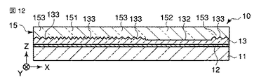
図11は、本発明の第2態様に係る光学素子を概略的に示す平面図である。図12は、図11に示す光学素子のXII−XII線に沿った断面図である。図13は、図11に示す光学素子のXIII−XIII線に沿った断面図である。図14は、図11に示す光学素子のXIV−XIV線に沿った断面図である。
Next, the second aspect of the present invention will be described.
FIG. 11 is a plan view schematically showing an optical element according to the second aspect of the present invention. 12 is a sectional view taken along line XII-XII of the optical element shown in FIG. 13 is a cross-sectional view taken along line XIII-XIII of the optical element shown in FIG. 14 is a cross-sectional view of the optical element shown in FIG. 11 taken along line XIV-XIV.
この光学素子10は、以下の構成を採用したこと以外は、図1乃至図3を参照しながら説明した光学素子10と同様の構造を有している。すなわち、この光学素子10では、凹部形成層13の前面は、凹部形成領域133をさらに含んでいる。以下、液晶層15のうち領域133上に形成された部分を、液晶部分153と呼ぶ。また、光学素子10のうち液晶部分153に対応した領域を、表示部103と呼ぶ。
This
領域133は、平面形状及び溝の長さ方向が異なること以外は、領域131及び132と同様の構造を有している。ここでは、一例として、領域133に設けた溝の長さ方向は、前面側から見てX方向に対して時計回りに45°の角度を為しているとする。
The
この光学素子10に白色光を照射し、これを正面から肉眼で観察した場合、表示部101乃至103は虹色に見える。また、表示部101乃至103は回折格子を構成している溝の長さ方向が異なっているので、通常の環境中では、それらを互いから判別することができる。
When this
次に、偏光子を介して光学素子10を観察した場合に見える画像について説明する。ここでは、一例として、偏光子として直線偏光フィルムを使用することとする。
Next, an image that is seen when the
図15は、図11乃至図14に示す光学素子と直線偏光フィルムとを重ねた場合に観察可能な像の一例を概略的に示す平面図である。 FIG. 15 is a plan view schematically showing an example of an image that can be observed when the optical element shown in FIGS. 11 to 14 and the linearly polarizing film are overlaid.
図15では、図11乃至図14に示す光学素子10と偏光フィルム50とを、偏光フィルム50側から光学素子10を見た場合に、偏光フィルム50の透過軸がX方向に対して時計回りに45°の角度を為すように重ねている。このような配置を採用し、これを正面から観察すると、図15に示すように、表示部101及び102は表示部103からの識別が可能であり、表示部101及び102は互いからの判別が不可能又は困難である。そして、表示部103は、銀色に見える。これについて、より詳細に説明する。なお、表示部101及び102の表示色は図8を参照しながら説明した通りであるので、ここでは、表示部103の表示色についてのみ説明する。
In FIG. 15, when the
領域133に設けた溝の長さ方向は、前面側から見てX方向に対して時計回りに45°の角度を為している。すなわち、液晶部分153の遅相軸は、偏光フィルム50の透過軸と平行である。それゆえ、表示部103は、偏光フィルム50が射出した光を、その偏光面を回転させることなしに反射する。この反射光は、理想的には吸収されることなしに偏光フィルム50を透過する。そのため、表示部103は、着色せずに、銀色に見える。
The length direction of the groove provided in the
図16は、図11乃至図14に示す光学素子が表示する像の他の例を示す斜視図である。 FIG. 16 is a perspective view showing another example of an image displayed by the optical element shown in FIGS.
図16に示すように、図15に示す状態から観察方向をX方向に垂直な面内で傾けると、図9を参照しながら説明したのと同様に、表示部101及び102の表示色が互いに異なる色へと変化する。他方、表示部103の表示色は、変化せず、銀色のままである。
As shown in FIG. 16, when the observation direction is tilted in the plane perpendicular to the X direction from the state shown in FIG. 15, the display colors of the
また、図16に示す状態から、光学素子10を偏光フィルム50と重ねたまま、その法線の周りで90°回転させると、図10を参照しながら説明したのと同様に、表示部101と表示部102との間で表示色が入れ替わる。他方、表示部103の表示色は、変化せず、銀色のままである。
Further, from the state shown in FIG. 16, when the
このように、図11乃至図14を参照しながら説明した光学素子10は、図1乃至図3を参照しながら説明した光学素子10と比較して、観察条件に応じてより多様に変化する像を表示する。この光学素子10は、例えば、図1乃至図3を参照しながら説明した光学素子10について例示した特徴に加え、以下の特徴を有している。
As described above, the
・表示部103は、偏光フィルム50なしで法線方向から観察した場合に、虹色を表示する。
・表示部103は、偏光フィルム50なしで法線方向から観察した場合に、表示部101及び102からの判別が可能である。
・表示部103は、偏光フィルム50を介して法線方向から観察した場合に、表示部101及び102とは異なる色を表示する。
The
The
The
上記のように、図11乃至図14に示す光学素子10が表示する像は観察条件に応じて多様に変化するので、この光学素子10は、例えば、優れた偽造防止効果、装飾効果及び/又は美的効果を提供する。
As described above, since the image displayed by the
例えば、この光学素子10とこれを支持した物品とを含んだラベル付き物品を真正品とした場合、真正であるか否かが未知の物品が上述した特徴の1つ以上を示さないときには、その物品は非真正品であると判断することができる。すなわち、真正であるか否かが未知の物品を真正品と非真正品との間で判別することができる。したがって、例えば、有価証券、銀行券、身分証明書などの証明書、及びクレジットカードなどの印刷物や美術品などの高級品の偽造を防止又は抑制することができる。また、この光学素子10と偏光フィルム50とを含んだ光学キットは、先の真偽判定に利用可能であるのに加え、玩具、学習教材又は装飾品等としても利用することができる。
For example, when a labeled article including the
次に、本発明の第3態様について説明する。
図17は、本発明の第3態様に係る光学素子を概略的に示す平面図である。図18は、図17に示す光学素子のXVIII−XVIII線に沿った断面図である。
Next, the third aspect of the present invention will be described.
FIG. 17 is a plan view schematically showing an optical element according to the third aspect of the present invention. 18 is a cross-sectional view taken along line XVIII-XVIII of the optical element shown in FIG.
この光学素子10は、以下の構成を採用したこと以外は、図11乃至図14を参照しながら説明した光学素子10と同様の構造を有している。
This
すなわち、この光学素子10では、凹部形成層13の前面は、凹部形成領域132の代わりに凹部形成領域134を含んでいる。凹部形成領域134は、平面形状が異なること以外は、凹部形成領域131と同様である。以下、液晶層15のうち領域134上に形成された部分を、液晶部分154と呼ぶ。また、光学素子10のうち液晶部分154に対応した領域を、表示部104と呼ぶ。
That is, in the
また、この光学素子では、凹部形成層13のうち、凹部形成領域134に対応した部分は、凹部形成領域131及び133に対応した部分と比較してより薄い。そして、液晶部分154は、液晶部分151及び153と比較してより厚い。
In this optical element, the portion corresponding to the
この光学素子10は、肉眼で観察した場合、表示部101及び103は、図11乃至図14を参照しながら説明した光学素子10と同様の像を表示する。そして、表示部104は、表示部101が表示する像とは判別が不可能であるか又は困難である虹色の像を表示する。
When the
次に、偏光子を介して光学素子10を観察した場合に見える画像について説明する。ここでは、一例として、偏光子として直線偏光フィルムを使用することとする。
Next, an image that is seen when the
図19は、図17及び図18に示す光学素子と直線偏光フィルムとを重ねた場合に観察可能な像の一例を概略的に示す平面図である。 FIG. 19 is a plan view schematically showing an example of an image that can be observed when the optical element shown in FIGS. 17 and 18 and a linearly polarizing film are overlaid.
図19では、図17及び図18に示す光学素子10と偏光フィルム50とを、偏光フィルム50側から光学素子10を見た場合に、偏光フィルム50の透過軸がX方向に対して時計回りに45°の角度を為すように重ねている。このような配置を採用し、これを正面から観察すると、図19に示すように、表示部101、103及び104は互いからの判別が可能である。これについて、より詳細に説明する。
In FIG. 19, when the
表示部101及び103の表示色は、図15を参照しながら説明した通りである。すなわち、表示部101は着色して見え、表示部103は銀色に見える。
The display colors of the
表示部104も表示部101と同様に着色して見えるが、液晶部分151と液晶部分154とは厚さが異なっている。等式(1)及び(2)を用いた説明から明らかなように、光学素子10と偏光フィルム50とを重ね、これらを正面から観察したときに表示部101及び104が表示する色は、液晶部分151及び154の厚さdに依存する。したがって、表示部101及び104は、異なる色を表示する。
Although the
図20は、図17及び図18に示す光学素子と直線偏光フィルムとを重ねた場合に観察可能な像の他の例を概略的に示す平面図である。
図20に示すように、図19に示す状態から観察方向をX方向に垂直な面内で傾けると、表示部101及び104の表示色が変化する。例えば、表示部101の表示色は緑色から紫色に変化し、表示部104の表示色はオレンジ色から黄色に変化する。他方、表示部103の表示色は、変化せず、銀色のままである。
FIG. 20 is a plan view schematically showing another example of an image that can be observed when the optical element shown in FIGS. 17 and 18 and a linearly polarizing film are overlaid.
As shown in FIG. 20, when the observation direction is tilted in a plane perpendicular to the X direction from the state shown in FIG. 19, the display colors of the
また、図20に示す状態から、光学素子10を偏光フィルム50と重ねたまま、その法線の周りで90°回転させると、表示部101及び104の表示色が変化する。他方、表示部103の表示色は、変化せず、銀色のままである。
In addition, when the
このように、図17及び図18を参照しながら説明した光学素子10は、図11乃至図14を参照しながら説明した光学素子10とは、観察条件に応じた像の変化が異なる。この光学素子10が表示する像は、例えば、以下のように、観察条件に応じて多様に変化する。
As described above, the
・表示部101及び104は、偏光フィルム50なしで法線方向から観察した場合に、虹色を表示する。
・表示部101及び104は、偏光フィルム50なしで法線方向から観察した場合に、互いからの判別が不可能又は困難である。したがって、表示部101及び104で潜像を形成することができる。
The
When the
・表示部101及び104は、偏光フィルム50を介して法線方向から観察した場合に、互いに異なる色を表示する。
・表示部101及び104は、偏光フィルム50を介して斜め方向から観察した場合に、互いに異なる色を表示する。
・表示部101及び104は、偏光フィルム50を介して法線方向から観察した場合と、偏光フィルム50を介して斜め方向から観察した場合とで異なる色を表示する。
The
The
The
・表示部101及び104は、偏光フィルム50の位置及び方位を固定し、光学素子10をその法線の周りで回転させながら偏光フィルム50を介して斜め方向から観察した場合に色変化を生じる。
・表示部101及び104は、光学素子10の位置及び方位を固定し、偏光フィルム50をその法線の周りで回転させながら、これを介して斜め方向から観察した場合に色変化を生じる。
The
The
・表示部103は、偏光フィルム50なしで法線方向から観察した場合に、虹色を表示する。
・表示部103は、偏光フィルム50なしで法線方向から観察した場合に、表示部101及び104からの判別が可能である。
・表示部103は、偏光フィルム50を介して法線方向から観察した場合に、表示部101及び104とは異なる色を表示する。
The
The
The
したがって、この光学素子10も、図1及び図2を参照しながら説明した光学素子10並びに図11乃至図14を参照しながら説明した光学素子10と同様に、例えば、優れた偽造防止効果、装飾効果及び/又は美的効果を提供する。それゆえ、この光学素子10とこれを支持した物品とを含んだラベル付き物品を真正品とした場合、真正であるか否かが未知の物品が上述した特徴の1つ以上を示さないときには、その物品は非真正品であると判断することができる。すなわち、真正であるか否かが未知の物品を真正品と非真正品との間で判別することができる。また、この光学素子10と偏光フィルム50とを含んだ光学キットは、先の真偽判定に利用可能であるのに加え、玩具、学習教材又は装飾品等としても利用することができる。
Therefore, this
液晶部分151と液晶部分154とで厚さを異ならしめる場合、それらの厚さの差は、例えば、0.1μm乃至5μmの範囲内とする。この差が小さいと、偏光フィルム50を介して観察した場合に、表示部101と表示部104とを互いから判別することが難しくなる。この差が大きいと、より厚い液晶部分において、高い秩序度でメソゲン基を配向させることが難しくなる。その結果、偏光フィルム50を介して観察した場合に、設計通りの色を表示させることが難しくなる。
When the thicknesses of the
次に、本発明の第4態様について説明する。
図21は、本発明の第4態様に係る光学素子を概略的に示す平面図である。図22は、図21に示す光学素子のXXII−XXII線に沿った断面図である。図23は、図21に示す光学素子のXXIII−XXIII線に沿った断面図である。
Next, the fourth aspect of the present invention will be described.
FIG. 21 is a plan view schematically showing an optical element according to the fourth aspect of the present invention. 22 is a cross-sectional view of the optical element shown in FIG. 21 taken along line XXII-XXII. 23 is a cross-sectional view of the optical element shown in FIG. 21 taken along line XXIII-XXIII.
この光学素子10は、以下の構成を採用したこと以外は、図1乃至図3を参照しながら説明した光学素子10と同様の構造を有している。
This
すなわち、この光学素子10では、凹部形成層13の前面は、凹部形成領域132の代わりに領域135を含んでいる。領域135は、溝が設けられていない領域であって、典型的には平坦である。以下、液晶層15のうち領域135上に形成された部分を、液晶部分155と呼ぶ。また、光学素子10のうち液晶部分155に対応した領域を、表示部105と呼ぶ。
That is, in this
液晶部分155では、液晶部分151と比較してメソゲン基がより低い秩序度で配向しているか、又は、メソゲン基は配向していない。すなわち、液晶部分155は、光学的に略等方性である。
In the
なお、典型的には、液晶部分155では、メソゲン基は僅かに配向している。すなわち、典型的には、液晶部分155は、光学的に僅かに異方性である。その理由を以下に説明する。
Typically, in the
凹部形成層13の前面に溝を設けた場合、それら溝の上部では、メソゲン基の配向には、溝が大きな影響を与える。これに対し、液晶層15の下地が平坦であり且つ配向処理が施されていない場合、メソゲン基の配向に、液晶層15の形成方法が影響を及ぼすことがある。例えば、液晶層15の材料を一方向に塗布したときには、液晶層15の下地が平坦であり且つ配向処理が施されていない場合であっても、メソゲン基が僅かに配向することがある。
When grooves are provided on the front surface of the
このような理由で、液晶部分155においてメソゲン基が僅かに配向し、その結果、液晶部分155が光学的に僅かに異方性を有することがある。ここでは、一例として、液晶部分155は、光学的に僅かに異方性であり、X方向に平行な遅相軸を有していることとする。
For this reason, the mesogenic group is slightly aligned in the
この光学素子10は、肉眼で観察した場合、表示部101は、図1乃至図3を参照しながら説明した光学素子10と同様の像を表示する。すなわち、表示部101は、虹色に見える。他方、表示部105は、領域135に回折格子が設けられていないので、干渉色は見えず、銀色に見える。すなわち、肉眼で観察した場合、表示部101及び105は、互いからの判別が容易である。
When the
次に、偏光子を介して光学素子10を観察した場合に見える画像について説明する。ここでは、一例として、偏光子として直線偏光フィルムを使用することとする。
Next, an image that is seen when the
図24は、図21乃至図23に示す光学素子と直線偏光フィルムとを重ねた場合に観察可能な像の一例を概略的に示す平面図である。 FIG. 24 is a plan view schematically showing an example of an image that can be observed when the optical element shown in FIGS. 21 to 23 and a linearly polarizing film are overlaid.
図24では、図21乃至図23に示す光学素子10と偏光フィルム50とを、偏光フィルム50側から光学素子10を見た場合に、偏光フィルム50の透過軸がX方向に対して時計回りに45°の角度を為すように重ねている。このような配置を採用し、これを正面から観察すると、表示部101は、図18を参照しながら説明したのと同様に、着色して見える。他方、表示部105は、液晶部分155が光学的に略等方性であるので、ほぼ銀色に見える。なお、表示部105が銀色ではなくほぼ銀色に見えるのは、液晶部分155においてメソゲン基が僅かに配向しているためである。
In FIG. 24, when the
図25は、図21乃至図23に示す光学素子と直線偏光フィルムとを重ねた場合に観察可能な像の他の例を概略的に示す平面図である。
図25に示すように、図24に示す状態から観察方向をX方向に垂直な面内で傾けると、表示部101の表示色が変化する。他方、表示部105の表示色は、ほぼ銀色のまま僅かに変化する。
FIG. 25 is a plan view schematically showing another example of an image that can be observed when the optical element shown in FIGS. 21 to 23 and a linearly polarizing film are overlaid.
As shown in FIG. 25, when the observation direction is tilted in a plane perpendicular to the X direction from the state shown in FIG. 24, the display color of the
また、図25に示す状態から、光学素子10を偏光フィルム50と重ねたまま、その法線の周りで90°回転させると、表示部101の表示色が変化する。他方、表示部105の表示色は、ほぼ銀色のまま僅かに変化する。例えば、表示部101は紫色から黄色へと変化し、表示部105は薄い紫色から薄い黄色へと変化する。
In addition, when the
なお、図25に示す状態から、光学素子10のみをその法線の周りで90°回転させると、表示部101は表示色を大きく変化させ、表示部105の表示色は、ほぼ銀色のまま僅かに変化する。例えば、表示部101は赤色から緑色へと変化し、表示部105は薄い紫色から薄い黄色へと変化する。
25, when only the
また、図21乃至図23に示す光学素子10と偏光フィルム50とを、偏光フィルム50の透過軸がX方向と平行となるように重ねた場合、表示部101は銀色に見える。この場合、液晶部分155の遅相軸は偏光フィルム50と透過軸と平行となるが、液晶部分155ではメソゲン基の配向秩序度が低いため、表示部105は、完全には着色が消えず、例えば薄い緑色に見える。
Further, when the
このように、表示部105は、肉眼で観察した場合と偏光フィルム50を介して観察した場合との双方において、表示部101とは著しく異なる視覚効果を与える。したがって、肉眼で観察した場合と偏光フィルム50を介して観察した場合との双方において、視認性に優れた像を表示することができる。すなわち、表示部105を設けることにより、意匠性を著しく高めることができる。
Thus, the
上述した光学素子10には、様々な変形が可能である。
例えば、図1及び図2を参照しながら説明した光学素子10、図11乃至図14を参照しながら説明した光学素子10、又は図21乃至図23を参照しながら説明した光学素子10は、液晶層15は、厚さが互いに異なる2つ以上の部分を含んでいてもよい。この場合、凹部形成層13の前面であって厚さが互いに異なる液晶部分に対応した領域に設けられた溝は、長さ方向が互いに等しくてもよく、異なっていてもよい。
Various modifications can be made to the
For example, the
また、図1及び図2を参照しながら説明した光学素子10、図11乃至図14を参照しながら説明した光学素子10、又は図17及び図18を参照しながら説明した光学素子10は、図21乃至図23を参照しながら説明した表示部105をさらに含んでいてもよい。こうすると、より複雑な像を表示でき、より高い意匠性を達成できる。
The
このように、上述した技術は、互いに組み合わせることができる。これにより、光学素子10が表示する像の観察条件に応じた変化の多様性をさらに高めることや、より高い意匠性を達成することが可能となる。
Thus, the above-described techniques can be combined with each other. Thereby, it is possible to further increase the diversity of changes according to the viewing conditions of the image displayed by the
光学素子10は、反射層12と凹部形成層13との間に、光学的に略等方性の透明又は半透明層をさらに含んでいてもよい。そのような中間層を使用すると、反射層12と凹部形成層13との密着性を向上させることができる。
The
光学素子10は、以下に説明する保護層や粘着層をさらに含んでいてもよい。
図26は、図1乃至図3に示す光学素子の一変形例を示す断面図である。
図26に示す光学素子10は、液晶層15を被覆した保護層16をさらに含んでいること以外は、図1乃至図3を参照しながら説明した光学素子10と同様の構造を有している。保護層16を設けると、液晶層15などの損傷や光劣化を生じ難くすることができ、それゆえ、光学素子10が表示する像の劣化を抑制することができる。
The
FIG. 26 is a cross-sectional view showing a modification of the optical element shown in FIGS.
The
保護層16の材料としては、例えば、耐傷性に優れたハードコート材料を使用することができる。また、保護層16の材料としては、典型的には、透明性の高い材料を使用する。保護層16は、無色透明であってもよく、有色透明であってもよい。
As a material of the
図27は、図1乃至図3に示す光学素子の他の変形例を示す断面図である。
図27に示す光学素子10は、基材11の裏面を被覆した粘着層17をさらに含んでいること以外は、図26を参照しながら説明した光学素子10と同様の構造を有している。この光学素子10は、物品に貼り付けて使用する用途に適している。なお、粘着層17は、剥離紙で被覆してもよい。
FIG. 27 is a cross-sectional view showing another modification of the optical element shown in FIGS.
The
偏光子として、偏光フィルム50を使用する代わりに、板状の偏光子などの他の形態の偏光子を使用してもよい。また、直線偏光子の代わりに、円偏光子又は楕円偏光子を使用してもよい。この場合、直線偏光子を使用した場合とは異なる色変化を観察できる。したがって、より複雑な視覚効果が得られる。
以下に、出願当初の特許請求の範囲に記載していた発明を付記する。
[1]長さ方向が揃い且つ前記長さ方向と交差する方向に隣り合った複数の溝が各々に設けられた1つ以上の凹部形成領域を一方の主面が含んだ光透過性の凹部形成層と、前記主面に支持されると共に固化された液晶材料からなる液晶層と、前記凹部形成層の他方の主面と向き合った鏡面反射層とを具備したことを特徴とする光学素子。
[2]前記1つ以上の凹部形成領域の少なくとも1つにおいて、前記複数の溝は回折格子又は一方向性拡散パターンを形成していることを特徴とする項1に記載の光学素子。
[3]前記1つ以上の凹部形成領域の少なくとも1つにおいて、前記複数の溝は回折格子を形成していることを特徴とする項1に記載の光学素子。
[4]前記液晶層は膜厚が互いに異なる複数の部分を含んだことを特徴とする項1乃至3の何れか1項に記載の光学素子。
[5]前記一方の主面は前記凹部形成領域を複数含み、それら複数の凹部形成領域の2つ以上は前記長さ方向が互いに等しく、前記長さ方向が互いに等しい2つ以上の凹部形成領域にそれぞれ対応した前記液晶層の複数の部分の2つ以上は厚さが互いに異なっていることを特徴とする項1乃至3の何れか1項に記載の光学素子。
[6]前記一方の主面は溝が設けられていない領域をさらに含んだことを特徴とする項1乃至5の何れか1項に記載の光学素子。
[7]前記一方の主面は前記凹部形成領域を複数含み、それら複数の凹部形成領域のうち、少なくとも1つの凹部形成領域は他の凹部形成領域とは前記長さ方向が異なっていることを特徴とする項1乃至6の何れか1項に記載の光学素子。
[8]前記鏡面反射層は金属反射層を含んだことを特徴とする項1乃至7の何れか1項に記載の光学素子。
[9]前記鏡面反射層は1層又は多層の誘電体膜を含んだことを特徴とする項1乃至7の何れか1項記載の光学素子。
[10]項1乃至9の何れか1項に記載の光学素子と、これを支持した物品とを含んだことを特徴とするラベル付き物品。
[11]項1乃至9の何れか1項に記載の光学素子と偏光子とを含んだことを特徴とする光学キット。
[12]真正であるか否かが未知の物品を真正品と非真正品との間で判別する方法であって、前記真正品は項1乃至9の何れか1項に記載の光学素子を支持した物品であり、前記真正であるか否かが未知の物品が、偏光子なしで観察したときに干渉光又は散乱光を表示光として射出し、前記偏光子を介して前記主面に対して垂直な方向から観察したときに前記偏光子なしで前記一方の主面に対して垂直な方向から観察したときとは異なる色を表示し、前記偏光子を介して前記一方の主面に対して傾いた方向から観察したときに前記偏光子なしで前記一方の主面に対して垂直な方向から観察したとき及び前記偏光子を介して前記主面に対して垂直な方向から観察したときとは異なる色を表示する表示部を含んでいない場合に、前記真正であるか否かが未知の物品は非真正品であると判断することを含んだことを特徴とする判別方法。
[13]前記真正であるか否かが未知の物品が前記表示部を含んでいた場合であって、前記真正であるか否かが未知の物品を前記一方の主面の法線の周りで回転させながら前記偏光子を介して前記一方の主面に対して傾いた方向から観察したときに、前記表示部の視覚効果に変化を生じない場合に、前記真正であるか否かが未知の物品は非真正品であると判断することをさらに含んだことを特徴とする項12に記載の判別方法。
Instead of using the
The invention described in the scope of claims at the beginning of the application will be appended.
[1] A light-transmitting recess having one main surface including one or more recess-forming regions each having a plurality of grooves that are aligned in the length direction and are adjacent to each other in a direction intersecting the length direction. An optical element comprising: a forming layer; a liquid crystal layer made of a liquid crystal material supported and solidified by the main surface; and a specular reflection layer facing the other main surface of the recess forming layer.
[2] The optical element according to [1], wherein the plurality of grooves form a diffraction grating or a unidirectional diffusion pattern in at least one of the one or more recess forming regions.
[3] The optical element according to
[4] The optical element according to any one of [1] to [3], wherein the liquid crystal layer includes a plurality of portions having different thicknesses.
[5] The one main surface includes a plurality of the recess formation regions, and two or more of the plurality of recess formation regions have the same length direction and two or more recess formation regions having the same length direction. Item 4. The optical element according to any one of
[6] The optical element according to any one of [1] to [5], wherein the one main surface further includes a region where no groove is provided.
[7] The one main surface includes a plurality of the recessed portion forming regions, and among the plurality of recessed portion forming regions, at least one recessed portion forming region has a different length direction from the other recessed portion forming regions. Item 7. The optical element according to any one of
[8] The optical element according to any one of [1] to [7], wherein the specular reflection layer includes a metal reflection layer.
[9] The optical element as described in any one of [1] to [7], wherein the specular reflection layer includes one or more dielectric films.
[10] A labeled article comprising the optical element according to any one of
[11] An optical kit comprising the optical element according to any one of
[12] A method for discriminating between an authentic product and an unauthentic product as to whether or not it is an authentic product, wherein the authentic product is the optical element according to any one of
[13] In the case where an article with unknown authenticity includes the display unit, the article with unknown unknown whether the authenticity is around the normal of the one main surface It is unknown whether the image is genuine or not when the visual effect of the display unit does not change when observed from a direction inclined with respect to the one main surface through the polarizer while rotating.
10…光学素子、11…基材、12…反射層、13…凹部形成層、15…液晶層、16…保護層、17…粘着層、50…偏光フィルム、101…表示部、102…表示部、103…表示部、104…表示部、105…表示部、131…領域、132…領域、133…領域、134…領域、135…領域、151…液晶部分、152…液晶部分、153…液晶部分、154…液晶部分、155…液晶部分。
DESCRIPTION OF
Claims (11)
前記凹部形成層の前記一方の主面に支持されると共に固化された液晶材料からなる液晶層と、
前記凹部形成層の他方の主面と向き合った鏡面反射層と
を具備し、前記複数の凹部形成領域において、一の凹部形成領域の複数の溝は、長さ方向、深さ及び/又は幅が、他の凹部形成領域の複数の溝と異なり、前記1つ又は複数の凹部形成領域の少なくとも1つには、前記複数の溝として、幅方向に隣り合う溝間の距離が不均一であり、一方向性拡散パターンを形成しているもののみが設けられていることを特徴とする光学素子。 A light-transmissive recess forming layer, the main surface of the one, a plurality of grooves adjacent in a direction intersecting the longitudinal direction with each longitudinal has it assortment each provided with 1 and a concave portion forming layer I contains a One or more recesses forming region,
A liquid crystal layer made of a liquid crystal material supported and solidified by the one main surface of the recess forming layer ;
A mirror reflection layer facing the other main surface of the recess forming layer, and in the plurality of recess forming regions, the plurality of grooves in one recess forming region have a length direction, a depth and / or a width. In addition, unlike the plurality of grooves in the other recess forming region, at least one of the one or more recess forming regions has a non-uniform distance between adjacent grooves in the width direction as the plurality of grooves. An optical element characterized in that only one that forms a unidirectional diffusion pattern is provided.
前記真正品は請求項1乃至7の何れか1項に記載の光学素子を支持した物品であり、
前記真正であるか否かが未知の物品が、偏光子なしで観察したときに散乱光を表示光として射出し、前記偏光子を介して前記主面に対して垂直な方向から観察したときに前記偏光子なしで前記一方の主面に対して垂直な方向から観察したときとは異なる色を表示し、前記偏光子を介して前記一方の主面に対して傾いた方向から観察したときに前記偏光子なしで前記一方の主面に対して垂直な方向から観察したとき及び前記偏光子を介して前記主面に対して垂直な方向から観察したときとは異なる色を表示する表示部を含んでいない場合に、前記真正であるか否かが未知の物品は非真正品であると判断することを含んだことを特徴とする判別方法。 It is a method for discriminating between an authentic product and an unauthentic product for an article whose authenticity is unknown,
The genuine product is an article that supports the optical element according to any one of claims 1 to 7,
When an article of which the authenticity is unknown is observed without a polarizer, scattered light is emitted as display light, and when observed from a direction perpendicular to the main surface through the polarizer When a color different from that observed when viewed from a direction perpendicular to the one principal surface without the polarizer is displayed, and when observed from a direction inclined with respect to the one principal surface via the polarizer A display unit that displays a color different from that observed from a direction perpendicular to the one main surface without the polarizer and from a direction perpendicular to the main surface via the polarizer; A determination method comprising: determining that an article of which the authenticity is unknown or not is an unauthentic product when not included.
Priority Applications (1)
| Application Number | Priority Date | Filing Date | Title |
|---|---|---|---|
| JP2007154555A JP5380791B2 (en) | 2007-06-11 | 2007-06-11 | Optical element, labeled article, optical kit, and discrimination method |
Applications Claiming Priority (1)
| Application Number | Priority Date | Filing Date | Title |
|---|---|---|---|
| JP2007154555A JP5380791B2 (en) | 2007-06-11 | 2007-06-11 | Optical element, labeled article, optical kit, and discrimination method |
Publications (2)
| Publication Number | Publication Date |
|---|---|
| JP2008304873A JP2008304873A (en) | 2008-12-18 |
| JP5380791B2 true JP5380791B2 (en) | 2014-01-08 |
Family
ID=40233630
Family Applications (1)
| Application Number | Title | Priority Date | Filing Date |
|---|---|---|---|
| JP2007154555A Expired - Fee Related JP5380791B2 (en) | 2007-06-11 | 2007-06-11 | Optical element, labeled article, optical kit, and discrimination method |
Country Status (1)
| Country | Link |
|---|---|
| JP (1) | JP5380791B2 (en) |
Families Citing this family (3)
| Publication number | Priority date | Publication date | Assignee | Title |
|---|---|---|---|---|
| JP5382315B2 (en) * | 2008-02-20 | 2014-01-08 | 株式会社三洋物産 | Game machine |
| JP5516065B2 (en) * | 2010-05-21 | 2014-06-11 | 凸版印刷株式会社 | Authenticity judgment method |
| JP5834683B2 (en) * | 2011-09-21 | 2015-12-24 | 凸版印刷株式会社 | Anti-counterfeit medium, authenticity determination method thereof, and manufacturing method of anti-counterfeit medium |
Family Cites Families (5)
| Publication number | Priority date | Publication date | Assignee | Title |
|---|---|---|---|---|
| JP4674829B2 (en) * | 1999-04-21 | 2011-04-20 | Jx日鉱日石エネルギー株式会社 | Optical laminate |
| JP2001091715A (en) * | 1999-09-27 | 2001-04-06 | Nippon Mitsubishi Oil Corp | Composite diffraction device |
| JP2004029189A (en) * | 2002-06-24 | 2004-01-29 | Dainippon Printing Co Ltd | Optical phase conversion body, light selecting/transmitting body, method and system for visualizing latent image |
| DE10318157A1 (en) * | 2003-04-17 | 2004-11-11 | Leonhard Kurz Gmbh & Co. Kg | Foil and optical fuse element |
| DE10328744A1 (en) * | 2003-06-25 | 2005-01-13 | Metronic Ag | Print carrier with optically birefringent layer |
-
2007
- 2007-06-11 JP JP2007154555A patent/JP5380791B2/en not_active Expired - Fee Related
Also Published As
| Publication number | Publication date |
|---|---|
| JP2008304873A (en) | 2008-12-18 |
Similar Documents
| Publication | Publication Date | Title |
|---|---|---|
| EP2068208B1 (en) | Optical element, article having label attached thereon, optical kit and discriminating method | |
| JP5045328B2 (en) | Optical element, labeled article, optical kit, and discrimination method | |
| JP5239509B2 (en) | Optical element, labeled article and optical kit | |
| RU2443004C2 (en) | Optical security marking component, method of manufacturing such a component, system comprising such a component, and reader for checking such a component | |
| JP5245296B2 (en) | Anti-counterfeit medium and discrimination method | |
| JP5211474B2 (en) | Laminated body, adhesive label, recording medium, and labeled article | |
| JP5125418B2 (en) | Optical element, labeled article, optical kit, and discrimination method | |
| JP5381023B2 (en) | Image forming body | |
| JP4978403B2 (en) | Optical element, labeled article, optical kit, and discrimination method | |
| JP5141078B2 (en) | Security device, printed matter with label and identification method | |
| JP5250991B2 (en) | Security device, verification method thereof and printed matter | |
| JP5343373B2 (en) | Security devices and labeled items | |
| JP2009078418A (en) | Security device, verifying method therefor, and printed matter | |
| JP5380791B2 (en) | Optical element, labeled article, optical kit, and discrimination method | |
| JP5211473B2 (en) | Laminated body, adhesive label, recording medium, and labeled article | |
| JP2009098568A (en) | Forgery prevention body, method for authenticity determination of forgery prevention body, forgery prevention label, and forgery prevention printed matter | |
| JP5315793B2 (en) | Security devices and labeled items | |
| JP5343384B2 (en) | Security devices and labeled items | |
| JP5245473B2 (en) | Security devices and labeled items | |
| JP5169463B2 (en) | Security devices and labeled items | |
| JP5141108B2 (en) | Optical element, labeled article, optical kit, and discrimination method | |
| JP5028643B2 (en) | Laminated body, adhesive label, recording medium, labeled article and discrimination method | |
| JP5659786B2 (en) | Laminated body and method for producing the same |
Legal Events
| Date | Code | Title | Description |
|---|---|---|---|
| A621 | Written request for application examination |
Free format text: JAPANESE INTERMEDIATE CODE: A621 Effective date: 20100524 |
|
| A521 | Written amendment |
Free format text: JAPANESE INTERMEDIATE CODE: A523 Effective date: 20110524 |
|
| A977 | Report on retrieval |
Free format text: JAPANESE INTERMEDIATE CODE: A971007 Effective date: 20111021 |
|
| A131 | Notification of reasons for refusal |
Free format text: JAPANESE INTERMEDIATE CODE: A131 Effective date: 20111108 |
|
| A521 | Written amendment |
Free format text: JAPANESE INTERMEDIATE CODE: A523 Effective date: 20111228 |
|
| RD04 | Notification of resignation of power of attorney |
Free format text: JAPANESE INTERMEDIATE CODE: A7424 Effective date: 20120529 |
|
| A131 | Notification of reasons for refusal |
Free format text: JAPANESE INTERMEDIATE CODE: A131 Effective date: 20120828 |
|
| A521 | Written amendment |
Free format text: JAPANESE INTERMEDIATE CODE: A523 Effective date: 20121024 |
|
| A131 | Notification of reasons for refusal |
Free format text: JAPANESE INTERMEDIATE CODE: A131 Effective date: 20130326 |
|
| A521 | Written amendment |
Free format text: JAPANESE INTERMEDIATE CODE: A523 Effective date: 20130524 |
|
| TRDD | Decision of grant or rejection written | ||
| A01 | Written decision to grant a patent or to grant a registration (utility model) |
Free format text: JAPANESE INTERMEDIATE CODE: A01 Effective date: 20130903 |
|
| A61 | First payment of annual fees (during grant procedure) |
Free format text: JAPANESE INTERMEDIATE CODE: A61 Effective date: 20130916 |
|
| R150 | Certificate of patent or registration of utility model |
Ref document number: 5380791 Country of ref document: JP Free format text: JAPANESE INTERMEDIATE CODE: R150 Free format text: JAPANESE INTERMEDIATE CODE: R150 |
|
| LAPS | Cancellation because of no payment of annual fees |